EP3716741B1 - Verfahren zur herstellung einer dreidimensionalen mehrschichtigen elektronischen vorrichtung und dreidimensionale mehrschichtige elektronische vorrichtung - Google Patents
Verfahren zur herstellung einer dreidimensionalen mehrschichtigen elektronischen vorrichtung und dreidimensionale mehrschichtige elektronische vorrichtung Download PDFInfo
- Publication number
- EP3716741B1 EP3716741B1 EP17932653.3A EP17932653A EP3716741B1 EP 3716741 B1 EP3716741 B1 EP 3716741B1 EP 17932653 A EP17932653 A EP 17932653A EP 3716741 B1 EP3716741 B1 EP 3716741B1
- Authority
- EP
- European Patent Office
- Prior art keywords
- layer
- unit
- forming
- electronic component
- electronic device
- Prior art date
- Legal status (The legal status is an assumption and is not a legal conclusion. Google has not performed a legal analysis and makes no representation as to the accuracy of the status listed.)
- Active
Links
Images




Classifications
-
- H—ELECTRICITY
- H05—ELECTRIC TECHNIQUES NOT OTHERWISE PROVIDED FOR
- H05K—PRINTED CIRCUITS; CASINGS OR CONSTRUCTIONAL DETAILS OF ELECTRIC APPARATUS; MANUFACTURE OF ASSEMBLAGES OF ELECTRICAL COMPONENTS
- H05K3/00—Apparatus or processes for manufacturing printed circuits
- H05K3/46—Manufacturing multilayer circuits
- H05K3/4644—Manufacturing multilayer circuits by building the multilayer layer by layer, i.e. build-up multilayer circuits
- H05K3/4664—Adding a circuit layer by thick film methods, e.g. printing techniques or by other techniques for making conductive patterns by using pastes, inks or powders
-
- B—PERFORMING OPERATIONS; TRANSPORTING
- B22—CASTING; POWDER METALLURGY
- B22F—WORKING METALLIC POWDER; MANUFACTURE OF ARTICLES FROM METALLIC POWDER; MAKING METALLIC POWDER; APPARATUS OR DEVICES SPECIALLY ADAPTED FOR METALLIC POWDER
- B22F10/00—Additive manufacturing of workpieces or articles from metallic powder
- B22F10/10—Formation of a green body
-
- B—PERFORMING OPERATIONS; TRANSPORTING
- B22—CASTING; POWDER METALLURGY
- B22F—WORKING METALLIC POWDER; MANUFACTURE OF ARTICLES FROM METALLIC POWDER; MAKING METALLIC POWDER; APPARATUS OR DEVICES SPECIALLY ADAPTED FOR METALLIC POWDER
- B22F10/00—Additive manufacturing of workpieces or articles from metallic powder
- B22F10/20—Direct sintering or melting
- B22F10/25—Direct deposition of metal particles, e.g. direct metal deposition [DMD] or laser engineered net shaping [LENS]
-
- B—PERFORMING OPERATIONS; TRANSPORTING
- B22—CASTING; POWDER METALLURGY
- B22F—WORKING METALLIC POWDER; MANUFACTURE OF ARTICLES FROM METALLIC POWDER; MAKING METALLIC POWDER; APPARATUS OR DEVICES SPECIALLY ADAPTED FOR METALLIC POWDER
- B22F7/00—Manufacture of composite layers, workpieces, or articles, comprising metallic powder, by sintering the powder, with or without compacting wherein at least one part is obtained by sintering or compression
- B22F7/02—Manufacture of composite layers, workpieces, or articles, comprising metallic powder, by sintering the powder, with or without compacting wherein at least one part is obtained by sintering or compression of composite layers
-
- B—PERFORMING OPERATIONS; TRANSPORTING
- B29—WORKING OF PLASTICS; WORKING OF SUBSTANCES IN A PLASTIC STATE IN GENERAL
- B29C—SHAPING OR JOINING OF PLASTICS; SHAPING OF MATERIAL IN A PLASTIC STATE, NOT OTHERWISE PROVIDED FOR; AFTER-TREATMENT OF THE SHAPED PRODUCTS, e.g. REPAIRING
- B29C64/00—Additive manufacturing, i.e. manufacturing of three-dimensional [3D] objects by additive deposition, additive agglomeration or additive layering, e.g. by 3D printing, stereolithography or selective laser sintering
- B29C64/30—Auxiliary operations or equipment
- B29C64/386—Data acquisition or data processing for additive manufacturing
-
- B—PERFORMING OPERATIONS; TRANSPORTING
- B33—ADDITIVE MANUFACTURING TECHNOLOGY
- B33Y—ADDITIVE MANUFACTURING, i.e. MANUFACTURING OF THREE-DIMENSIONAL [3D] OBJECTS BY ADDITIVE DEPOSITION, ADDITIVE AGGLOMERATION OR ADDITIVE LAYERING, e.g. BY 3D PRINTING, STEREOLITHOGRAPHY OR SELECTIVE LASER SINTERING
- B33Y10/00—Processes of additive manufacturing
-
- B—PERFORMING OPERATIONS; TRANSPORTING
- B33—ADDITIVE MANUFACTURING TECHNOLOGY
- B33Y—ADDITIVE MANUFACTURING, i.e. MANUFACTURING OF THREE-DIMENSIONAL [3D] OBJECTS BY ADDITIVE DEPOSITION, ADDITIVE AGGLOMERATION OR ADDITIVE LAYERING, e.g. BY 3D PRINTING, STEREOLITHOGRAPHY OR SELECTIVE LASER SINTERING
- B33Y50/00—Data acquisition or data processing for additive manufacturing
- B33Y50/02—Data acquisition or data processing for additive manufacturing for controlling or regulating additive manufacturing processes
-
- H—ELECTRICITY
- H05—ELECTRIC TECHNIQUES NOT OTHERWISE PROVIDED FOR
- H05K—PRINTED CIRCUITS; CASINGS OR CONSTRUCTIONAL DETAILS OF ELECTRIC APPARATUS; MANUFACTURE OF ASSEMBLAGES OF ELECTRICAL COMPONENTS
- H05K1/00—Printed circuits
- H05K1/18—Printed circuits structurally associated with non-printed electric components
- H05K1/182—Printed circuits structurally associated with non-printed electric components associated with components mounted in printed circuit boards [PCB], e.g. insert-mounted components [IMC]
- H05K1/185—Printed circuits structurally associated with non-printed electric components associated with components mounted in printed circuit boards [PCB], e.g. insert-mounted components [IMC] associated with components encapsulated in the insulating substrate of the PCBs; associated with components incorporated in internal layers of multilayer circuit boards
- H05K1/186—Printed circuits structurally associated with non-printed electric components associated with components mounted in printed circuit boards [PCB], e.g. insert-mounted components [IMC] associated with components encapsulated in the insulating substrate of the PCBs; associated with components incorporated in internal layers of multilayer circuit boards manufactured by mounting on or connecting to patterned circuits before or during embedding
-
- H—ELECTRICITY
- H05—ELECTRIC TECHNIQUES NOT OTHERWISE PROVIDED FOR
- H05K—PRINTED CIRCUITS; CASINGS OR CONSTRUCTIONAL DETAILS OF ELECTRIC APPARATUS; MANUFACTURE OF ASSEMBLAGES OF ELECTRICAL COMPONENTS
- H05K3/00—Apparatus or processes for manufacturing printed circuits
- H05K3/46—Manufacturing multilayer circuits
-
- H—ELECTRICITY
- H05—ELECTRIC TECHNIQUES NOT OTHERWISE PROVIDED FOR
- H05K—PRINTED CIRCUITS; CASINGS OR CONSTRUCTIONAL DETAILS OF ELECTRIC APPARATUS; MANUFACTURE OF ASSEMBLAGES OF ELECTRICAL COMPONENTS
- H05K3/00—Apparatus or processes for manufacturing printed circuits
- H05K3/46—Manufacturing multilayer circuits
- H05K3/4611—Manufacturing multilayer circuits by laminating two or more circuit boards
- H05K3/4614—Manufacturing multilayer circuits by laminating two or more circuit boards the electrical connections between the circuit boards being made during lamination
-
- H—ELECTRICITY
- H05—ELECTRIC TECHNIQUES NOT OTHERWISE PROVIDED FOR
- H05K—PRINTED CIRCUITS; CASINGS OR CONSTRUCTIONAL DETAILS OF ELECTRIC APPARATUS; MANUFACTURE OF ASSEMBLAGES OF ELECTRICAL COMPONENTS
- H05K3/00—Apparatus or processes for manufacturing printed circuits
- H05K3/46—Manufacturing multilayer circuits
- H05K3/4697—Manufacturing multilayer circuits having cavities, e.g. for mounting components
-
- B—PERFORMING OPERATIONS; TRANSPORTING
- B22—CASTING; POWDER METALLURGY
- B22F—WORKING METALLIC POWDER; MANUFACTURE OF ARTICLES FROM METALLIC POWDER; MAKING METALLIC POWDER; APPARATUS OR DEVICES SPECIALLY ADAPTED FOR METALLIC POWDER
- B22F7/00—Manufacture of composite layers, workpieces, or articles, comprising metallic powder, by sintering the powder, with or without compacting wherein at least one part is obtained by sintering or compression
- B22F7/02—Manufacture of composite layers, workpieces, or articles, comprising metallic powder, by sintering the powder, with or without compacting wherein at least one part is obtained by sintering or compression of composite layers
- B22F7/04—Manufacture of composite layers, workpieces, or articles, comprising metallic powder, by sintering the powder, with or without compacting wherein at least one part is obtained by sintering or compression of composite layers with one or more layers not made from powder, e.g. made from solid metal
- B22F2007/042—Manufacture of composite layers, workpieces, or articles, comprising metallic powder, by sintering the powder, with or without compacting wherein at least one part is obtained by sintering or compression of composite layers with one or more layers not made from powder, e.g. made from solid metal characterised by the layer forming method
- B22F2007/047—Manufacture of composite layers, workpieces, or articles, comprising metallic powder, by sintering the powder, with or without compacting wherein at least one part is obtained by sintering or compression of composite layers with one or more layers not made from powder, e.g. made from solid metal characterised by the layer forming method non-pressurised baking of the paste or slurry containing metal powder
-
- B—PERFORMING OPERATIONS; TRANSPORTING
- B22—CASTING; POWDER METALLURGY
- B22F—WORKING METALLIC POWDER; MANUFACTURE OF ARTICLES FROM METALLIC POWDER; MAKING METALLIC POWDER; APPARATUS OR DEVICES SPECIALLY ADAPTED FOR METALLIC POWDER
- B22F2998/00—Supplementary information concerning processes or compositions relating to powder metallurgy
- B22F2998/10—Processes characterised by the sequence of their steps
-
- B—PERFORMING OPERATIONS; TRANSPORTING
- B22—CASTING; POWDER METALLURGY
- B22F—WORKING METALLIC POWDER; MANUFACTURE OF ARTICLES FROM METALLIC POWDER; MAKING METALLIC POWDER; APPARATUS OR DEVICES SPECIALLY ADAPTED FOR METALLIC POWDER
- B22F7/00—Manufacture of composite layers, workpieces, or articles, comprising metallic powder, by sintering the powder, with or without compacting wherein at least one part is obtained by sintering or compression
- B22F7/06—Manufacture of composite layers, workpieces, or articles, comprising metallic powder, by sintering the powder, with or without compacting wherein at least one part is obtained by sintering or compression of composite workpieces or articles from parts, e.g. to form tipped tools
- B22F7/08—Manufacture of composite layers, workpieces, or articles, comprising metallic powder, by sintering the powder, with or without compacting wherein at least one part is obtained by sintering or compression of composite workpieces or articles from parts, e.g. to form tipped tools with one or more parts not made from powder
-
- B—PERFORMING OPERATIONS; TRANSPORTING
- B33—ADDITIVE MANUFACTURING TECHNOLOGY
- B33Y—ADDITIVE MANUFACTURING, i.e. MANUFACTURING OF THREE-DIMENSIONAL [3D] OBJECTS BY ADDITIVE DEPOSITION, ADDITIVE AGGLOMERATION OR ADDITIVE LAYERING, e.g. BY 3D PRINTING, STEREOLITHOGRAPHY OR SELECTIVE LASER SINTERING
- B33Y80/00—Products made by additive manufacturing
-
- H—ELECTRICITY
- H05—ELECTRIC TECHNIQUES NOT OTHERWISE PROVIDED FOR
- H05K—PRINTED CIRCUITS; CASINGS OR CONSTRUCTIONAL DETAILS OF ELECTRIC APPARATUS; MANUFACTURE OF ASSEMBLAGES OF ELECTRICAL COMPONENTS
- H05K2203/00—Indexing scheme relating to apparatus or processes for manufacturing printed circuits covered by H05K3/00
- H05K2203/01—Tools for processing; Objects used during processing
- H05K2203/0104—Tools for processing; Objects used during processing for patterning or coating
- H05K2203/013—Inkjet printing, e.g. for printing insulating material or resist
-
- H—ELECTRICITY
- H05—ELECTRIC TECHNIQUES NOT OTHERWISE PROVIDED FOR
- H05K—PRINTED CIRCUITS; CASINGS OR CONSTRUCTIONAL DETAILS OF ELECTRIC APPARATUS; MANUFACTURE OF ASSEMBLAGES OF ELECTRICAL COMPONENTS
- H05K2203/00—Indexing scheme relating to apparatus or processes for manufacturing printed circuits covered by H05K3/00
- H05K2203/01—Tools for processing; Objects used during processing
- H05K2203/0147—Carriers and holders
- H05K2203/0156—Temporary polymeric carrier or foil, e.g. for processing or transferring
-
- H—ELECTRICITY
- H05—ELECTRIC TECHNIQUES NOT OTHERWISE PROVIDED FOR
- H05K—PRINTED CIRCUITS; CASINGS OR CONSTRUCTIONAL DETAILS OF ELECTRIC APPARATUS; MANUFACTURE OF ASSEMBLAGES OF ELECTRICAL COMPONENTS
- H05K2203/00—Indexing scheme relating to apparatus or processes for manufacturing printed circuits covered by H05K3/00
- H05K2203/06—Lamination
- H05K2203/061—Lamination of previously made multilayered subassemblies
-
- H—ELECTRICITY
- H05—ELECTRIC TECHNIQUES NOT OTHERWISE PROVIDED FOR
- H05K—PRINTED CIRCUITS; CASINGS OR CONSTRUCTIONAL DETAILS OF ELECTRIC APPARATUS; MANUFACTURE OF ASSEMBLAGES OF ELECTRICAL COMPONENTS
- H05K3/00—Apparatus or processes for manufacturing printed circuits
- H05K3/0097—Processing two or more printed circuits simultaneously, e.g. made from a common substrate, or temporarily stacked circuit boards
-
- H—ELECTRICITY
- H05—ELECTRIC TECHNIQUES NOT OTHERWISE PROVIDED FOR
- H05K—PRINTED CIRCUITS; CASINGS OR CONSTRUCTIONAL DETAILS OF ELECTRIC APPARATUS; MANUFACTURE OF ASSEMBLAGES OF ELECTRICAL COMPONENTS
- H05K3/00—Apparatus or processes for manufacturing printed circuits
- H05K3/46—Manufacturing multilayer circuits
- H05K3/4644—Manufacturing multilayer circuits by building the multilayer layer by layer, i.e. build-up multilayer circuits
- H05K3/4682—Manufacture of core-less build-up multilayer circuits on a temporary carrier or on a metal foil
-
- Y—GENERAL TAGGING OF NEW TECHNOLOGICAL DEVELOPMENTS; GENERAL TAGGING OF CROSS-SECTIONAL TECHNOLOGIES SPANNING OVER SEVERAL SECTIONS OF THE IPC; TECHNICAL SUBJECTS COVERED BY FORMER USPC CROSS-REFERENCE ART COLLECTIONS [XRACs] AND DIGESTS
- Y02—TECHNOLOGIES OR APPLICATIONS FOR MITIGATION OR ADAPTATION AGAINST CLIMATE CHANGE
- Y02P—CLIMATE CHANGE MITIGATION TECHNOLOGIES IN THE PRODUCTION OR PROCESSING OF GOODS
- Y02P10/00—Technologies related to metal processing
- Y02P10/25—Process efficiency
Definitions
- the present disclosure relates to a method of manufacturing a three-dimensional multi-layer electronic device using three-dimensional lay-out forming, and a three-dimensional multi-layer electronic device.
- a technology disclosed in Patent Literature 1 is a high-speed prototype forming method, including: a. a process of electrolyzing an object into relatively thick multiple layers; b. a process of electrically slicing the multiple layers into multiple cross-sections corresponding to the thickness of an assembly material sheet; and c. a process of drawing, on a sheet, a physical section of the assembly material corresponding the cross-sections.
- the high-speed prototype forming method further includes: d. a process of slicing the physical sections from the assembly material sheet; e. a process of laying out the physical sections to assemble the layers; and f. a process of reforming a physical model of the object by laying out the layers.
- Patent Literature 1 JP-T-H11-514304
- Patent Literature 1 can avoid sequentially forming layers, for example, one by one at one time.
- the technology since the technology relates to a prototype modeling technology, it is difficult to apply the technology to manufacturing of a three-dimensional multi-layer electronic device.
- a component is built in a cavity by a full additive method, it is complicated to consider a dimensional variation of the built-in component. This is because it is necessary to adjust the dimension of a cavity one by one according to a component variation, and further to adjust the amount of a resin embedded in the cavity.
- the present disclosure has been made in view of the above-described points, and an object of the present disclosure is to provide a method of manufacturing a three-dimensional multi-layer electronic device and a three-dimensional multi-layer electronic device that can reduce a tact time and a cycle time. Further, another object of the present disclosure is to provide a method of manufacturing a three-dimensional multi-layer electronic device and a three-dimensional multi-layer electronic device that can have a high tolerance for a dimensional variation of embedded electronic components.
- the present specification discloses a method of manufacturing a three-dimensional multi-layer electronic device as defined in claim 1, the method including: a unit forming process of forming a multi-layer unit including an electronic component and a circuit wiring by three-dimensional lay-out forming; and a unit lay-out process of manufacturing a three-dimensional multi-layer electronic device by laying out the multi-layer units integrally in a vertical direction.
- a method of manufacturing a three-dimensional multi-layer electronic device can shorten a tact time and a cycle time. Further, according to the present disclosure, it is possible to have a high tolerance for dimensional variations of built-in electronic components.
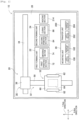
- Multi-layer unit forming device 10 includes conveying device 20, first forming unit 22, second forming unit 24, mounting unit 26, and control device (see Figs. 2 and 3 ) 27.
- Multi-layer unit forming device 10 further includes transfer unit 200 and heating section 214.
- Conveying device 20, first forming unit 22, second forming unit 24, mounting unit 26, transfer unit 200, and heating section 214 are arranged on base 28 of multi-layer unit forming device 10.
- Base 28 has a rectangular shape in general, and in the following description, the longitudinal direction of base 28 is referred to as an X-axis direction, the short-side direction of base 28 is referred to as a Y-axis direction, and a direction orthogonal to both the X-axis direction and the Y-axis direction is referred to as a Z-axis direction.
- Conveying device 20 includes X-axis slide mechanism 30 and Y-axis slide mechanism 32.
- X-axis slide mechanism 30 includes X-axis slide rail 34 and X-axis slider 36.
- X-axis slide rail 34 is disposed on base 28 to extend in the X-axis direction.
- X-axis slider 36 is slidably held in the X-axis direction by X-axis slide rail 34.
- X-axis slide mechanism 30 has electromagnetic motor (see Fig. 2 ) 38, and X-axis slider 36 is moved to a predetermined position in the X-axis direction by driving electromagnetic motor 38.
- Y-axis slide mechanism 32 has Y-axis slide rail 50 and stage 52.
- Y-axis slide rail 50 is disposed on base 28 to extend in the Y-axis direction.
- One end of Y-axis slide rail 50 is connected to X-axis slider 36. Therefore, Y-axis slide rail 50 is movable in the X-axis direction.
- Stage 52 is held on Y-axis slide rail 50 to be slidable in the Y-axis direction.
- Y-axis slide mechanism 32 has electromagnetic motor (see Fig. 2 ) 56, and stage 52 is moved to a predetermined position in the Y-axis direction by driving electromagnetic motor 56. Accordingly, stage 52 is moved to a predetermined position on base 28 by driving X-axis slide mechanism 30 and Y-axis slide mechanism 32.
- Stage 52 includes base 60, holding devices 62, and lifting and lowering device 64.
- Base 60 is formed in a flat plate shape, and base material (see Fig. 5 ) 70 is placed on the upper surface of base 60.
- Holding devices 62 are provided on both sides of base 60 in the X-axis direction. Both edge portions of base material 70 placed on base 60 in the X-axis direction are sandwiched by holding devices 62, so that base material 70 is fixedly held.
- Lifting and lowering device 64 is disposed below base 60, and lifts and lowers base 60 in the Z-axis direction.
- base material 70 A material made of a wax-based material (for example, a brazing material) soluble by heat or a solvent is used as base material 70.
- base material 70 is not limited thereto, and may be made of, for example, a strippable base material (for example, a double-sided tape, a film material or the like having a low adhesive force).
- a strippable base material for example, a double-sided tape, a film material or the like having a low adhesive force.
- base material 70 is fixedly held on base 60 by the adhesive force, and thus, holding devices 62 become unnecessary.
- First forming unit 22 is a unit for forming a circuit wiring on base material 70 mounted on base 60 of stage 52, and includes first printing section 72 and sintering section 74.
- First printing section 72 has inkjet head (see Fig. 2 ) 76, and linearly ejects metal ink onto base material 70 placed on base 60.
- the metal ink is obtained by dispersing fine particles of metal in a solvent.
- Inkjet head 76 ejects metal ink from multiple nozzles by, for example, a piezo method using a piezoelectric element.
- Sintering section 74 has laser irradiation device (see Fig. 2 ) 78.
- Laser irradiation device 78 is a device for irradiating the metal ink ejected onto base material 70 with a laser beam, and the metal ink irradiated with the laser is sintered to form the circuit wiring.
- Sintering of the metal ink is a phenomenon in which evaporation of a solvent, decomposition of protective films of metal microparticles, or the like is performed by applying energy, and the metal microparticles contact or are fused with each other, so that conductivity is increased. Then, the metal ink is sintered to form a circuit wiring made of metal.
- second forming unit 24 is a unit for forming a resin layer on base material 70 placed on base 60 of stage 52, and includes second printing section 84 and curing section 86.
- Second printing section 84 includes inkjet head (see Fig. 2 ) 88, and ejects an ultraviolet curable resin onto base material 70 placed on base 60.
- the ultraviolet curable resin is a resin that is cured by irradiation with ultraviolet rays.
- Inkjet head 88 may be, for example, a piezo type using a piezoelectric element, or may be a thermal type in which a resin is heated to generate air bubbles, which are ejected from multiple nozzles.
- Curing section 86 includes flattening device (see Fig. 2 ) 90 and irradiation device (see Fig. 2 ) 92.
- Flattening device 90 flattens the upper surface of the ultraviolet curable resin ejected onto base material 70 by inkjet head 88, and for example, scrapes off excess resin by a roller or a blade while smoothening the surface of the ultraviolet curable resin, to make the thickness of the ultraviolet curable resin uniform.
- irradiation device 92 includes a mercury lamp or an LED as a light source, and irradiates the ultraviolet curable resin ejected onto base material 70 with ultraviolet rays. Accordingly, the ultraviolet curable resin ejected onto base material 70 is cured to form a resin layer.
- mounting unit 26 is a unit for mounting first electronic component (see Fig. 7 ) 96, second electronic component (see Fig. 7 ) 98, and probe pin (see Fig. 7 ) 99 on base material 70 placed on base 60 of stage 52, and has supply section 100 and mounting section 102.
- Supply section 100 has multiple first tape feeders (see Fig. 2 ) 110 for feeding taped first electronic component 96 one by one and multiple second tape feeders (see Fig. 2 ) 111 for feeding taped second electronic component 98 one by one, and supplies first electronic component 96 and second electronic component 98 at each supply position. Further, supply section 100 has tray (see Fig.
- first electronic component 96 and second electronic component 98 are not limited to supply by first tape feeders 110 and second tape feeders 111, but may be supplied by a tray.
- the supply of probe pin 99 is not limited to supply by tray 201, but may be supply by a tape feeder.
- first electronic component 96, second electronic component 98, and probe pin 99 may be supplied by both the tape feeder and the tray, or may be supplied by another method.
- Mounting section 102 has mounting head (see Fig. 2 ) 112 and moving device (see Fig. 2 ) 114.
- Mounting head 112 has suction nozzle 118 (see Fig. 7 ) for picking up and holding first electronic component 96, second electronic component 98, or probe pin 99 (hereinafter, referred to as the first electronic component 96 or the like).
- Suction nozzle 118 picks up and holds first electronic component 96 and the like by picking up air as a negative pressure is supplied from a positive/negative pressure supply device (not illustrated). As a slight positive pressure is supplied from the positive/negative pressure supply device, first electronic component 96 and the like are separated.
- moving device 114 moves mounting head 112 between each supply position or tray 201 of first tape feeder 110 and second tape feeder 111 and base material 70 placed on base 60. Accordingly, in mounting section 102, first electronic component 96 or the like is held by suction nozzle 118, and first electronic component 96 or the like held by suction nozzle 118 is mounted on base material 70.
- a sensor element such as a gyro sensor is used as first electronic component 96 or second electronic component 98.
- probe pin 99 may be a probe pin of which a tip end can be stroked, but such a stroke may not be possible.
- Transfer unit 200 is a unit for transferring first conductive adhesive 224 (see Fig. 5 ) and second conductive adhesive 234 (see Fig. 5 ) onto base material 70 placed on base 60 of stage 52.
- First conductive adhesive 224 and second conductive adhesive 234 are conductive pastes that are cured by heating.
- first conductive adhesive 224 is cured by ultraviolet ray before the heating. Irradiation of the ultraviolet rays is performed by irradiation device 92.
- transfer unit 200 includes supply section 202 and transfer section 204.
- Supply section 202 includes first adhesive supply device 206 (see Fig. 3 ) and second adhesive supply device 208 (see Fig. 3 ).
- First adhesive supply device 206 has a dip plate (not illustrated) onto which first conductive adhesive 224 is ejected, and supplies first conductive adhesive 224 in a state in which first conductive adhesive 224 has a uniform thickness by being pushed and spread by a squeegee (not illustrated) in the dip plate.
- second adhesive supply device 208 has a dip plate (not illustrated) onto which second conductive adhesive 234 is ejected, and supplies second conductive adhesive 234 in a state in which second conductive adhesive 234 has a uniform thickness by being extruded and spread by a squeegee (not illustrated) in the dip plate.
- Transfer section 204 includes transfer head 210 (see Fig. 3 ) and moving device (see Fig. 3 ) 212.
- Transfer head 210 has multiple dip needles (see Fig. 5 ) 119 for transferring first conductive adhesive 224 or second conductive adhesive 234. Dip needle 119 is dipped into first conductive adhesive 224 or second conductive adhesive 234 in each dip plate of first adhesive supply device 206 or second adhesive supply device 208. Accordingly, first conductive adhesive 224 or second conductive adhesive 234 adheres to a tip end of dip needle 119.
- Transfer head 210 uses multiple dip needles 119 separately to which first conductive adhesive 224 is attached and to which second conductive adhesive 234 is attached.
- transfer device 212 moves transfer head 210 between each dip plate of first adhesive supply device 206 or second adhesive supply device 208 and base material 70 mounted on base 60. Accordingly, in transfer section 204, first conductive adhesive 224 or second conductive adhesive 234 adhering to the tip end of dip needle 119 is transferred onto base material 70.
- Heating section 214 has irradiation device (see Fig. 3 ) 216.
- Irradiation device 216 includes an infrared lamp or an infrared heater, and irradiates base material 70 with infrared rays. Accordingly, first conductive adhesive 224 or second conductive adhesive 234 transferred onto base material 70 is cured by heating.
- Heating section 214 may include an electric furnace instead of irradiation device 216.
- control device 27 includes controller 120 and multiple driving circuits 122.
- multiple driving circuits 122 are connected to electromagnetic motors 38 and 56, holding device 62, lifting and lowering device 64, inkjet head 76, laser irradiation device 78, inkjet head 88, flattening device 90, irradiation device 92, first tape feeder 110, second tape feeder 111, mounting head 112, and moving device 114.
- multiple driving circuits 122 are connected to first adhesive supply device 206, second adhesive supply device 208, transfer head 210, moving device 212, and irradiation device 216.
- Controller 120 includes a CPU, a ROM, a RAM, and the like, mainly includes a computer, and is connected to multiple driving circuits 122. Accordingly, controller 120 controls operations of conveying device 20, first forming unit 22, second forming unit 24, mounting unit 26, transfer unit 200, and heating section 214.
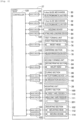
- method 130 of manufacturing a three-dimensional multi-layer electronic device includes unit forming process P10 and unit lay-out process P12.
- unit forming process P10 multi-layer units 218A, 218B, and 218C (see Fig. 7 ) are formed on base material 70 by multi-layer unit forming device 10.
- unit lay-out process P12 multi-layer units 218A, 218B, and 218C are laid out in a vertical direction, so that three-dimensional multi-layer electronic device 246 (see Fig. 9 ) is manufactured.
- multi-layer units 218A to 218C are collectively referred without distinction, multi-layer units 218A to 218C are referred to as multi-layer unit 218.
- Unit forming process P10 is executed by controller 120, and includes resin multi-layer forming process S10, conductive terminal forming process S20, circuit wiring forming process S30, and mounting process S40.
- An order of execution of steps S10, S20, S30, and S40 is determined by a multi-layer structure or the like of three-dimensional multi-layer electronic device 246 (that is, each of multi-layer units 218A to 218C). Therefore, steps S10, S20, S30, and S40 are not repeated in a notation order.
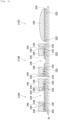
- unit lay-out process P12 when each of multi-layer units 218A to 218C illustrated in Figs. 5 to 7 is formed will be described.
- first resin layer 220 of multi-layer unit 218 is formed on base material 70. Therefore, base material 70 is set with respect to base 60. Stage 52 is moved below second forming unit 24. Thereafter, in second printing section 84, inkjet head 88 ejects the ultraviolet curable resin in a thin film shape onto the upper surface of base material 70. Subsequently, in curing section 86, flattening device 90 flattens the ejected ultraviolet curable resin such that the film thickness thereof becomes uniform. Further, irradiation device 92 irradiates the flattened ultraviolet curable resin with ultraviolet rays. Accordingly, the ultraviolet curable resin is cured. Thereafter, the ejection, the flattening, and the curing of the ultraviolet curable resin are repeated, so that first resin layer 220 is formed on base material 70 in multi-layer unit 218.
- Resin multi-layer forming step S10 includes space forming step S12 (see Fig. 4 ).
- space forming step S12 when the ejection, the flattening, and the curing of the ultraviolet curable resin are repeated, the inkjet head 88 ejects the ultraviolet curable resin such that a predetermined portion is exposed to the upper surface of base material 70 in a generally circular shape. Accordingly, multiple through-holes 222 are formed in resin layer 220 of each of multi-layer units 218B and 218C.
- stage 52 is moved below transfer unit 200.
- first conductive adhesive 224 supplied in first adhesive supply device 206 is attached to a tip end of dip needle 119 of transfer head 210. Attached first conductive adhesive 224 is filled in each through hole 222 of resin layer 220 as transfer head 210 is moved by moving device 212. Accordingly, in resin layer 220 of each of multi-layer units 218B and 218C, first conductive adhesive 224 is transferred to each through hole 222.
- stage 52 is moved to curing section 86 of second forming unit 24.
- irradiation device 92 irradiates transferred first conductive adhesive 224 with ultraviolet rays. Accordingly, in resin layer 220 of each of multi-layer units 218B and 218C, first conductive adhesive 224 in each through-hole 222 is cured to form each conductive terminal 226.
- stage 52 is moved below first forming unit 22.
- inkjet head 76 linearly ejects the metal ink onto the upper surface of resin layer 220 of multi-layer unit 218 according to a wiring circuit pattern.
- inkjet head 76 also ejects the metal ink onto the upper surface of conductive terminal 226 of each of multi-layer units 218B and 218C according to the wiring circuit pattern.
- laser irradiation device 78 irradiates the ejected metal ink with a laser beam.
- first circuit wiring 228 is formed on the upper surface of resin layer 220 of multi-layer unit 218 by sintering the metal ink. Circuit wiring 228 is also formed on the upper surface of conductive terminal 226 of each of multi-layer units 218B and 218C.
- resin multi-layer forming step S10 and circuit wiring forming step S30 are repeated. Accordingly, second resin layer 230 and second circuit wiring 232 are formed in each of multi-layer units 218A and 218B. On the other hand, in multi-layer unit 218C, second resin layer 230 is formed.
- Mounting step S40 includes transfer step S42 (see Fig. 4 ), mounting step S44 (see Fig. 4 ), and heating step S46 (see Fig. 4 ).
- stage 52 is moved below transfer unit 200.
- second conductive adhesive 234 supplied in second adhesive supply device 208 is attached to a tip end of dip needle 119 of transfer head 210. Attached second conductive adhesive 234 is transferred to multiple predetermined positions in each of multi-layer units 218A and 218B as transfer head 210 moves by moving device 212. Any of transferred second conductive adhesive 234 is filled up to the through-hole of second resin layer 230 in a gap of second circuit wiring 232, so that second circuit wiring 232 and first circuit wiring 228 are electrically connected to each other.
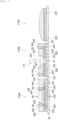
- third resin layer 236 is formed in multi-layer unit 218 as illustrated in Fig. 6 .
- third resin layer 236 is formed on the upper surface of second resin layer 230 or the upper surface of second circuit wiring 232.
- space 240 is formed at planned mounting position 238 of each of multi-layer units 218A and 218B by space forming step S12.
- third resin layer 236 is formed on the upper surface of second resin layer 230.
- the upper surface of third resin layer 236 is not flattened, but is formed in a dome shape.
- stage 52 is moved below mounting unit 26.
- first electronic component 96 supplied by first tape feeder 110 is held by suction nozzle 118 of mounting head 112.
- each electrode 97 of first electronic component 96 is arranged to face the lower side with straddling a gap of first circuit wiring 228, and is connected to the upper surface of each circuit wiring 228 forming the gap via second conductive adhesive 234.
- second conductive adhesive 234 has a structure in which circuit wirings 228 forming the gap are electrically connected to each other via first electronic component 96.
- First electronic component 96 is separated from third resin layer 236 forming the wall surface of space 240. Further, the upper surface of first electronic component 96 is located below the upper surface of third resin layer 236.
- second electronic component 98 supplied by second tape feeder 111 is held by suction nozzle 118 of mounting head 112.
- Held second electronic component 98 is mounted in space 240 of multi-layer unit 218A as mounting head 112 moves by moving device 114.
- each electrode (not illustrated) of second electronic component 98 faces the lower side and is connected to the upper surface of first circuit wiring 228 via second conductive adhesive 234.
- Multiple second electronic components 98 are mounted in space 240 of multi-layer unit 218A.
- Each of second electronic components 98 is in a state of being separated from third resin layer 236 forming the wall surface of space 240. Further, the upper surface of each second electronic component 98 is located below the upper surface of third resin layer 236.
- probe pin 99 supplied from tray 201 is held by suction nozzle 118 of mounting head 112.
- Held probe pin 99 is mounted in space 240 of each of multi-layer units 218A and 218B as mounting head 112 moves by moving device 114. Accordingly, multiple probe pins 99 are mounted on respective multi-layer units 218A and 218B.
- a lower end of probe pin 99 is connected to the upper surface of second circuit wiring 232 via second conductive adhesive 234.
- An upper end of probe pin 99 is located above the upper surface of third resin layer 236.
- stage 52 is moved below heating section 214.
- irradiation device 216 irradiates infrared rays onto base material 70. Accordingly, in each of multi-layer units 218A, 218B, and 218C, first conductive adhesive 224 and second conductive adhesive 234 are cured, and first electronic component 96, second electronic component 98, and probe pins 99 are fixed.
- Unit lay-out process P12 includes unit peeling step S50 and unit lay-out step S60.
- unit peeling step S50 base material 70 is melted by heat or a solvent. Accordingly, multi-layer units 218A, 218B, and 218C are separated from base material 70.
- multi-layer units 218A, 218B, and 218C are laid out in the vertical direction. Accordingly, as illustrated in Fig. 9 , each of multi-layer units 218A, 218B, and 218C is integrated into three-dimensional multi-layer electronic device 246.
- intermediate multi-layer unit 218B is laid out on lower multi-layer unit 218A.
- the upper end portion of each probe pin 99 of lower multi-layer unit 218A is brought into contact with each conductive terminal 226 of intermediate multi-layer unit 218B, and is further inserted into each conductive terminal 226.
- lower multi-layer unit 218A is electrically connected to intermediate multi-layer unit 218B.
- central space 240 of lower multi-layer unit 218A is closed by bottom surface 242 of intermediate multi-layer unit 218B. Accordingly, cavity portion 244 in which multiple second electronic components 98 are incorporated is formed in lower multi-layer unit 218A.
- Upper multi-layer unit 218C is laid out on intermediate multi-layer unit 218B. At this time, the upper end portion of each probe pin 99 of intermediate multi-layer unit 218B is brought into contact with each conductive terminal 226 of upper multi-layer unit 218C, and is further inserted into conductive terminal 226. Accordingly, intermediate multi-layer unit 218B is electrically connected to upper multi-layer unit 218C. Further, central space 240 of intermediate multi-layer unit 218B is closed by bottom surface 242 of upper multi-layer unit 218C. Accordingly, cavity portion 244 in which first electronic component 96 is incorporated is formed in intermediate multi-layer unit 218B.
- multi-layer units 218A, 218B, and 218C are integrated by a general method such as bonding, pressure bonding, or screw tightening (using an adhesive or a photocurable resin).
- three-dimensional multi-layer electronic device 246 is manufactured, so that a tact time and a cycle time of the manufacturing can be shortened.
- first electronic component 96, second electronic component 98, and probe pin 99 are examples of electronic components.
- Probe pin 99 is an example of a connection pin.
- Unit lay-out step S60 is an example of a cavity forming step.
- multi-layer unit 218B is laid out on multi-layer unit 218A
- multi-layer unit 218B is an example of an upper layer multi-layer unit
- multi-layer unit 218A is an example of a lower layer multi-layer unit.
- multi-layer unit 218C is laid out on multi-layer unit 218B
- multi-layer unit 218C is an example of an upper layer multi-layer unit
- multi-layer unit 218B is an example of a lower layer multi-layer unit.
- multi-layer units 218A, 218B, and 218C are collectively formed on base material 70.
- multi-layer units 218A, 218B, and 218C may be formed on (base material 70 of) a separate multi-layer unit forming device 10.
- three-dimensional multi-layer electronic device 246 is configured by three multi-layer units 218, but may be configured by two or four or more multi-layer units.
- the number of multi-layer units constituting three-dimensional multi-layer electronic device 246 is determined from the viewpoint of the number of layers of circuit wiring, the number of connection layers of electronic components, the tact time, or the like.
- first electronic component 96 is located below the upper surface of third resin layer 236, but may be located above the upper surface of third resin layer 236.
- upper multi-layer unit 218C is laid out on intermediate multi-layer unit 218B on bottom surface 242 of upper multi-layer unit 218C, a space facing space 240 in which first electronic component 96 is mounted is formed, and an upper portion of first electronic component 96 is accommodated in the space.
- sintering of the metal ink is performed by laser irradiation.
- the sintering of the metal ink may be performed collectively by a heating method using an electric furnace, an infrared heater, a hot plate or the like, depending on the type of the metal ink and a work size.
- first conductive adhesive 224 is cured by ultraviolet rays and heating and second conductive adhesive 234 is cured by heating.
- first conductive adhesive 224 and second conductive adhesive 234 may be cured by a laser, a flash lamp, or the like.
- multi-layer unit 218B with a multi-layer unit in which an electronic component different from first electronic component 96 is incorporated, or replace multi-layer unit 218B with a multi-layer unit in which a circuit wiring of a wiring circuit pattern different from circuit wirings 228 and 232 is formed.
- multi-layer unit 218D illustrated in Fig. 10 may be integrated with multi-layer units 218A and 218C.
- Multi-layer unit 218D differs from multi-layer unit 218B at least in terms of third electronic component 250 accommodated in central space 240 and a wiring circuit pattern of first layer circuit wiring 252 on which third electronic component 250 is mounted. Accordingly, in method 130 of manufacturing a three-dimensional multi-layer electronic device, three-dimensional multi-layer electronic device 254 illustrated in Fig. 11 , which is different from three-dimensional multi-layer electronic device 246 described above, is produced.
- Third electronic component 250 is an example of an electronic component.
- multi-layer unit 218A can be replaced with a multi-layer unit in which a circuit wiring having a wiring circuit pattern different from that of circuit wiring 228 is formed.
Landscapes
- Engineering & Computer Science (AREA)
- Manufacturing & Machinery (AREA)
- Chemical & Material Sciences (AREA)
- Materials Engineering (AREA)
- Microelectronics & Electronic Packaging (AREA)
- Mechanical Engineering (AREA)
- Physics & Mathematics (AREA)
- Optics & Photonics (AREA)
- Composite Materials (AREA)
- Production Of Multi-Layered Print Wiring Board (AREA)
- Printing Elements For Providing Electric Connections Between Printed Circuits (AREA)
- Manufacturing Of Printed Wiring (AREA)
Claims (3)
- Verfahren (130) zum Herstellen einer dreidimensionalen, mehrschichtigen elektronischen Vorrichtung (246), umfassend:einen Einheitenbildungsprozess (P10) zum Bilden von mehrschichtigen Einheiten (218A, 218B, 218C), umfassend eine elektronische Komponente (96, 98, 99) und eine Schaltungsverdrahtung (228, 232) durch Bilden eines dreidimensionalen Verlegens; undeinen Einheitenverlegeprozess (P12) zum Herstellen einer dreidimensionalen, mehrschichtigen elektronischen Vorrichtung (246) durch integrales Verlegen der mehrschichtigen Einheiten (218A, 218B, 218C) in einer vertikalen Richtung, wobei der Einheitenbildungsprozess (P10) umfasst:einen Harz-Mehrschichtbildungsschritt (S10) zum Bilden mehrerer Harzschichten (220, 230, 236) für jede mehrschichtige Einheit (218A, 218B, 218C) durch Ausstoßen von ultraviolett härtbarem Harz und anschließendes Abflachen und Härten des ultraviolett härtbaren Harzes,einen Leiteranschluss-Bildungsschritt (S20) zum Bilden eines leitenden Anschlusses (226) in einer mehrschichtigen Einheit (218B, 218C), die eine obere mehrschichtige Einheit (218B, 218C) sein soll, zum elektrischen Verbinden mit einer unteren mehrschichtigen Einheit (218A, 218B), wenn die mehrschichtigen Einheiten in der vertikalen Richtung verlegt sind, undeinen Schaltungsverdrahtungs-Bildungsschritt (S30) zum Bilden einer Schaltungsverdrahtung (228, 232) für jede mehrschichtige Einheit (218A, 218B, 218C) durch Ausstoßen von Metalltinte gemäß einem Verdrahtungsschaltungsmuster und anschließendes Sintern der Metalltinte,wobei die elektronische Komponente (96, 98, 99) einer mehrschichtigen Einheit (218A, 218B), die eine untere mehrschichtige Einheit (218A, 218B) sein soll, umfasst:
einen Verbindungsstift (99) zum elektrischen Verbinden mit einem leitenden Anschluss (226) einer oberen mehrschichtigen Einheit (218B, 218C), wenn die mehrschichtigen Einheiten in der vertikalen Richtung verlegt sind. - Verfahren zum Herstellen einer dreidimensionalen, mehrschichtigen elektronischen Vorrichtung nach Anspruch 1,
wobei der Einheitenbildungsprozess (P10) umfasst:einen Raumbildungsschritt (S12) zum Bilden eines Raums (240), in dem die elektronische Komponente (96, 98, 99) an einer geplanten Montageposition der elektronischen Komponente (96, 98, 99) angeordnet werden kann; undeinen Montageschritt (S44) zum Montieren der elektronischen Komponente (96, 98, 99) im Raum (240), undwobei der Einheitenverlegeprozess (P12) umfasst:
einen Hohlraum-Bildungsschritt (S60) zum Bilden eines Hohlraumabschnitts durch Schließen des Raums (240) durch eine Unterseite einer oberen mehrschichtigen Einheit (218B, 218C). - Verfahren zum Herstellen einer dreidimensionalen, mehrschichtigen elektronischen Vorrichtung nach Anspruch 1 oder 2,
wobei beim Einheitenverlegungsprozess (P12) wenigstens eine der in vertikaler Richtung integral auszulegenden mehrschichtigen Einheiten (218A, 218B, 218C) gemeinsam verwendet wird, so dass eine andere mehrschichtige Einheit (218A, 218B, 218C) als die gemeinsam verwendete mehrschichtige Einheit (218A, 218B, 218C) durch eine mehrschichtige Einheit (218A, 218B, 218C), umfassend eine elektronische Komponente (96, 98, 99), die sich von der elektronischen Komponente (96, 98, 99) unterscheidet, oder eine Schaltungsverdrahtung (228, 232) mit einem Muster, das sich von dem der Schaltungsverdrahtung (228, 232) unterscheidet, ersetzt wird, wodurch eine dreidimensionale, mehrschichtige elektronische Vorrichtung (246), die sich von der dreidimensionalen, mehrschichtigen elektronischen Vorrichtung (246) unterscheidet, hergestellt wird.
Applications Claiming Priority (1)
| Application Number | Priority Date | Filing Date | Title |
|---|---|---|---|
| PCT/JP2017/041814 WO2019102522A1 (ja) | 2017-11-21 | 2017-11-21 | 3次元積層電子デバイスの製造方法及び3次元積層電子デバイス |
Publications (3)
| Publication Number | Publication Date |
|---|---|
| EP3716741A1 EP3716741A1 (de) | 2020-09-30 |
| EP3716741A4 EP3716741A4 (de) | 2020-11-18 |
| EP3716741B1 true EP3716741B1 (de) | 2025-05-28 |
Family
ID=66631518
Family Applications (1)
| Application Number | Title | Priority Date | Filing Date |
|---|---|---|---|
| EP17932653.3A Active EP3716741B1 (de) | 2017-11-21 | 2017-11-21 | Verfahren zur herstellung einer dreidimensionalen mehrschichtigen elektronischen vorrichtung und dreidimensionale mehrschichtige elektronische vorrichtung |
Country Status (4)
| Country | Link |
|---|---|
| US (1) | US11458722B2 (de) |
| EP (1) | EP3716741B1 (de) |
| JP (1) | JP6947842B2 (de) |
| WO (1) | WO2019102522A1 (de) |
Families Citing this family (12)
| Publication number | Priority date | Publication date | Assignee | Title |
|---|---|---|---|---|
| US12520464B2 (en) | 2019-07-16 | 2026-01-06 | Fjui Corporation | Three-dimensional molding machine and component mounting machine |
| JP7145334B2 (ja) | 2019-07-30 | 2022-09-30 | 株式会社Fuji | 3次元積層造形による電子回路製造方法 |
| JP7130875B2 (ja) * | 2019-07-30 | 2022-09-05 | 株式会社Fuji | スタック部品の製造方法 |
| WO2021019707A1 (ja) | 2019-07-31 | 2021-02-04 | 株式会社Fuji | 3次元積層造形による回路配線の製造方法 |
| WO2021033228A1 (ja) * | 2019-08-19 | 2021-02-25 | 株式会社Fuji | 3次元積層造形による3次元積層電子デバイスの製造方法 |
| US11452199B2 (en) * | 2019-09-12 | 2022-09-20 | At&S Austria Technologie & Systemtechnik Aktiengesellschaft | Electronic module with single or multiple components partially surrounded by a thermal decoupling gap |
| DE202020100143U1 (de) * | 2020-01-10 | 2020-02-24 | Igus Gmbh | Kunststoff-Bauteile für Energieführungsketten mit integrierter Sensorik |
| JP7761585B2 (ja) * | 2020-11-10 | 2025-10-28 | 株式会社Fuji | 回路形成方法 |
| US12565006B2 (en) | 2020-11-20 | 2026-03-03 | Fuji Corporation | Production method and production device for three-dimensionally fabricated object |
| US20250226357A1 (en) | 2022-04-08 | 2025-07-10 | Fuji Corporation | Electrical circuit formation method and electrical circuit formation device |
| WO2024247233A1 (ja) * | 2023-06-01 | 2024-12-05 | 株式会社Fuji | 押圧装置 |
| WO2025191863A1 (ja) * | 2024-03-15 | 2025-09-18 | 株式会社Fuji | 印刷装置、情報処理装置、印刷システム、製造方法及び情報処理方法 |
Family Cites Families (17)
| Publication number | Priority date | Publication date | Assignee | Title |
|---|---|---|---|---|
| US5663883A (en) | 1995-08-21 | 1997-09-02 | University Of Utah Research Foundation | Rapid prototyping method |
| JPH09199526A (ja) * | 1996-01-18 | 1997-07-31 | Hitachi Ltd | 半導体装置 |
| US6038133A (en) * | 1997-11-25 | 2000-03-14 | Matsushita Electric Industrial Co., Ltd. | Circuit component built-in module and method for producing the same |
| JP2002359343A (ja) * | 2001-05-31 | 2002-12-13 | Nec Corp | 半導体装置 |
| JP2003100937A (ja) * | 2001-09-26 | 2003-04-04 | Hitachi Ltd | 高周波モジュール |
| US6860418B2 (en) * | 2002-07-19 | 2005-03-01 | Lockheed Martin Corporation | Method for making a bonding tool |
| AU2003900180A0 (en) * | 2003-01-16 | 2003-01-30 | Silverbrook Research Pty Ltd | Method and apparatus (dam001) |
| TWI263313B (en) | 2005-08-15 | 2006-10-01 | Phoenix Prec Technology Corp | Stack structure of semiconductor component embedded in supporting board |
| US20080186690A1 (en) * | 2007-02-07 | 2008-08-07 | Nokia Corporation | Electronics Package And Manufacturing Method Thereof |
| US7479794B2 (en) * | 2007-02-28 | 2009-01-20 | Sv Probe Pte Ltd | Spring loaded probe pin assembly |
| US20140246227A1 (en) * | 2013-03-01 | 2014-09-04 | Bridge Semiconductor Corporation | Method of making cavity substrate with built-in stiffener and cavity substrate manufactured thereby |
| TW201517240A (zh) * | 2013-10-16 | 2015-05-01 | 矽品精密工業股份有限公司 | 封裝結構及其製法 |
| US10667403B2 (en) | 2014-09-19 | 2020-05-26 | Fuji Corporation | Manufacturing apparatus for performing additive manufacturing of an electrical device |
| KR20170118837A (ko) | 2015-02-18 | 2017-10-25 | 옵토멕 인코포레이티드 | 단일 및 복수-층 전자 회로들의 부가적 제조 |
| WO2016147284A1 (ja) * | 2015-03-16 | 2016-09-22 | 富士機械製造株式会社 | 形成方法及び形成装置 |
| JP2017130553A (ja) * | 2016-01-20 | 2017-07-27 | 株式会社ミマキエンジニアリング | 電子素子設置基材の製造方法、電子部材の製造方法、及び造形装置 |
| KR102582421B1 (ko) * | 2016-01-29 | 2023-09-25 | 삼성전자주식회사 | 인쇄회로기판 및 이를 구비한 전자소자 패키지 |
-
2017
- 2017-11-21 EP EP17932653.3A patent/EP3716741B1/de active Active
- 2017-11-21 JP JP2019555101A patent/JP6947842B2/ja active Active
- 2017-11-21 WO PCT/JP2017/041814 patent/WO2019102522A1/ja not_active Ceased
- 2017-11-21 US US16/760,580 patent/US11458722B2/en active Active
Also Published As
| Publication number | Publication date |
|---|---|
| EP3716741A4 (de) | 2020-11-18 |
| US20200346452A1 (en) | 2020-11-05 |
| EP3716741A1 (de) | 2020-09-30 |
| US11458722B2 (en) | 2022-10-04 |
| JP6947842B2 (ja) | 2021-10-13 |
| JPWO2019102522A1 (ja) | 2020-11-26 |
| WO2019102522A1 (ja) | 2019-05-31 |
Similar Documents
| Publication | Publication Date | Title |
|---|---|---|
| US11458722B2 (en) | Three-dimensional multi-layer electronic device production method | |
| US11470724B2 (en) | Manufacturing apparatus for performing additive manufacturing of an electrical device | |
| JP6987975B2 (ja) | 3次元構造物形成方法、および3次元構造物形成装置 | |
| JP7316742B2 (ja) | 3次元積層造形による実装基板の製造方法 | |
| JP6533112B2 (ja) | 回路形成方法 | |
| US20210298180A1 (en) | Circuit forming method | |
| US20210267054A1 (en) | Circuit formation method and circuit formation device | |
| JP7543432B2 (ja) | 3次元造形物の製造方法、及び製造装置 | |
| US12539662B2 (en) | Molding method | |
| US20250113447A1 (en) | Electrical circuit forming method and electrical circuit forming apparatus | |
| US20250142734A1 (en) | Electrical circuit formation method, and electrical circuit formation device | |
| JP7282906B2 (ja) | 部品装着方法、および部品装着装置 | |
| US12096570B2 (en) | Wiring formation method | |
| JP7627570B2 (ja) | 3次元造形物製造装置及び表示方法 | |
| EP4529368A1 (de) | Herstellungsverfahren und herstellungsvorrichtung | |
| US12048102B2 (en) | Electronic circuit production method using 3D layer shaping | |
| EP4429412A1 (de) | Schaltungsherstellungsverfahren und schaltungsherstellungsvorrichtung | |
| JP7284275B2 (ja) | 3次元積層造形による3次元積層電子デバイスの製造方法 | |
| JP2023166848A (ja) | 電気回路形成方法、および電気回路形成装置 | |
| WO2023210021A1 (ja) | 塗布情報生成方法、情報処理装置及び3次元造形装置 |
Legal Events
| Date | Code | Title | Description |
|---|---|---|---|
| STAA | Information on the status of an ep patent application or granted ep patent |
Free format text: STATUS: THE INTERNATIONAL PUBLICATION HAS BEEN MADE |
|
| PUAI | Public reference made under article 153(3) epc to a published international application that has entered the european phase |
Free format text: ORIGINAL CODE: 0009012 |
|
| STAA | Information on the status of an ep patent application or granted ep patent |
Free format text: STATUS: REQUEST FOR EXAMINATION WAS MADE |
|
| 17P | Request for examination filed |
Effective date: 20200508 |
|
| AK | Designated contracting states |
Kind code of ref document: A1 Designated state(s): AL AT BE BG CH CY CZ DE DK EE ES FI FR GB GR HR HU IE IS IT LI LT LU LV MC MK MT NL NO PL PT RO RS SE SI SK SM TR |
|
| AX | Request for extension of the european patent |
Extension state: BA ME |
|
| A4 | Supplementary search report drawn up and despatched |
Effective date: 20201015 |
|
| RIC1 | Information provided on ipc code assigned before grant |
Ipc: H05K 3/46 20060101AFI20201009BHEP Ipc: H05K 1/18 20060101ALI20201009BHEP Ipc: B29C 64/112 20170101ALI20201009BHEP Ipc: B33Y 10/00 20150101ALI20201009BHEP Ipc: H05K 3/00 20060101ALN20201009BHEP Ipc: B33Y 80/00 20150101ALI20201009BHEP |
|
| DAV | Request for validation of the european patent (deleted) | ||
| DAX | Request for extension of the european patent (deleted) | ||
| STAA | Information on the status of an ep patent application or granted ep patent |
Free format text: STATUS: EXAMINATION IS IN PROGRESS |
|
| 17Q | First examination report despatched |
Effective date: 20220404 |
|
| P01 | Opt-out of the competence of the unified patent court (upc) registered |
Effective date: 20230328 |
|
| GRAP | Despatch of communication of intention to grant a patent |
Free format text: ORIGINAL CODE: EPIDOSNIGR1 |
|
| STAA | Information on the status of an ep patent application or granted ep patent |
Free format text: STATUS: GRANT OF PATENT IS INTENDED |
|
| RIC1 | Information provided on ipc code assigned before grant |
Ipc: B33Y 80/00 20150101ALN20250108BHEP Ipc: B22F 7/08 20060101ALN20250108BHEP Ipc: B22F 7/04 20060101ALN20250108BHEP Ipc: H05K 3/00 20060101ALN20250108BHEP Ipc: B33Y 10/00 20150101ALI20250108BHEP Ipc: B22F 10/25 20210101ALI20250108BHEP Ipc: B22F 10/10 20210101ALI20250108BHEP Ipc: B22F 7/02 20060101ALI20250108BHEP Ipc: H05K 1/18 20060101ALI20250108BHEP Ipc: H05K 3/46 20060101AFI20250108BHEP |
|
| INTG | Intention to grant announced |
Effective date: 20250120 |
|
| GRAS | Grant fee paid |
Free format text: ORIGINAL CODE: EPIDOSNIGR3 |
|
| GRAA | (expected) grant |
Free format text: ORIGINAL CODE: 0009210 |
|
| STAA | Information on the status of an ep patent application or granted ep patent |
Free format text: STATUS: THE PATENT HAS BEEN GRANTED |
|
| AK | Designated contracting states |
Kind code of ref document: B1 Designated state(s): AL AT BE BG CH CY CZ DE DK EE ES FI FR GB GR HR HU IE IS IT LI LT LU LV MC MK MT NL NO PL PT RO RS SE SI SK SM TR |
|
| REG | Reference to a national code |
Ref country code: GB Ref legal event code: FG4D |
|
| REG | Reference to a national code |
Ref country code: CH Ref legal event code: EP |
|
| REG | Reference to a national code |
Ref country code: IE Ref legal event code: FG4D Ref country code: DE Ref legal event code: R096 Ref document number: 602017089720 Country of ref document: DE |
|
| REG | Reference to a national code |
Ref country code: NL Ref legal event code: MP Effective date: 20250528 |
|
| PG25 | Lapsed in a contracting state [announced via postgrant information from national office to epo] |
Ref country code: FI Free format text: LAPSE BECAUSE OF FAILURE TO SUBMIT A TRANSLATION OF THE DESCRIPTION OR TO PAY THE FEE WITHIN THE PRESCRIBED TIME-LIMIT Effective date: 20250528 Ref country code: ES Free format text: LAPSE BECAUSE OF FAILURE TO SUBMIT A TRANSLATION OF THE DESCRIPTION OR TO PAY THE FEE WITHIN THE PRESCRIBED TIME-LIMIT Effective date: 20250528 |
|
| REG | Reference to a national code |
Ref country code: LT Ref legal event code: MG9D |
|
| PG25 | Lapsed in a contracting state [announced via postgrant information from national office to epo] |
Ref country code: NO Free format text: LAPSE BECAUSE OF FAILURE TO SUBMIT A TRANSLATION OF THE DESCRIPTION OR TO PAY THE FEE WITHIN THE PRESCRIBED TIME-LIMIT Effective date: 20250828 Ref country code: GR Free format text: LAPSE BECAUSE OF FAILURE TO SUBMIT A TRANSLATION OF THE DESCRIPTION OR TO PAY THE FEE WITHIN THE PRESCRIBED TIME-LIMIT Effective date: 20250829 |
|
| PG25 | Lapsed in a contracting state [announced via postgrant information from national office to epo] |
Ref country code: PL Free format text: LAPSE BECAUSE OF FAILURE TO SUBMIT A TRANSLATION OF THE DESCRIPTION OR TO PAY THE FEE WITHIN THE PRESCRIBED TIME-LIMIT Effective date: 20250528 Ref country code: NL Free format text: LAPSE BECAUSE OF FAILURE TO SUBMIT A TRANSLATION OF THE DESCRIPTION OR TO PAY THE FEE WITHIN THE PRESCRIBED TIME-LIMIT Effective date: 20250528 |
|
| PG25 | Lapsed in a contracting state [announced via postgrant information from national office to epo] |
Ref country code: BG Free format text: LAPSE BECAUSE OF FAILURE TO SUBMIT A TRANSLATION OF THE DESCRIPTION OR TO PAY THE FEE WITHIN THE PRESCRIBED TIME-LIMIT Effective date: 20250528 |
|
| PG25 | Lapsed in a contracting state [announced via postgrant information from national office to epo] |
Ref country code: HR Free format text: LAPSE BECAUSE OF FAILURE TO SUBMIT A TRANSLATION OF THE DESCRIPTION OR TO PAY THE FEE WITHIN THE PRESCRIBED TIME-LIMIT Effective date: 20250528 |
|
| PGFP | Annual fee paid to national office [announced via postgrant information from national office to epo] |
Ref country code: FR Payment date: 20250930 Year of fee payment: 9 |
|
| PG25 | Lapsed in a contracting state [announced via postgrant information from national office to epo] |
Ref country code: RS Free format text: LAPSE BECAUSE OF FAILURE TO SUBMIT A TRANSLATION OF THE DESCRIPTION OR TO PAY THE FEE WITHIN THE PRESCRIBED TIME-LIMIT Effective date: 20250828 |
|
| PG25 | Lapsed in a contracting state [announced via postgrant information from national office to epo] |
Ref country code: IS Free format text: LAPSE BECAUSE OF FAILURE TO SUBMIT A TRANSLATION OF THE DESCRIPTION OR TO PAY THE FEE WITHIN THE PRESCRIBED TIME-LIMIT Effective date: 20250928 |
|
| PG25 | Lapsed in a contracting state [announced via postgrant information from national office to epo] |
Ref country code: LV Free format text: LAPSE BECAUSE OF FAILURE TO SUBMIT A TRANSLATION OF THE DESCRIPTION OR TO PAY THE FEE WITHIN THE PRESCRIBED TIME-LIMIT Effective date: 20250528 |
|
| REG | Reference to a national code |
Ref country code: AT Ref legal event code: MK05 Ref document number: 1799398 Country of ref document: AT Kind code of ref document: T Effective date: 20250528 |
|
| PGFP | Annual fee paid to national office [announced via postgrant information from national office to epo] |
Ref country code: DE Payment date: 20250930 Year of fee payment: 9 |
|
| PG25 | Lapsed in a contracting state [announced via postgrant information from national office to epo] |
Ref country code: DK Free format text: LAPSE BECAUSE OF FAILURE TO SUBMIT A TRANSLATION OF THE DESCRIPTION OR TO PAY THE FEE WITHIN THE PRESCRIBED TIME-LIMIT Effective date: 20250528 Ref country code: SM Free format text: LAPSE BECAUSE OF FAILURE TO SUBMIT A TRANSLATION OF THE DESCRIPTION OR TO PAY THE FEE WITHIN THE PRESCRIBED TIME-LIMIT Effective date: 20250528 Ref country code: AT Free format text: LAPSE BECAUSE OF FAILURE TO SUBMIT A TRANSLATION OF THE DESCRIPTION OR TO PAY THE FEE WITHIN THE PRESCRIBED TIME-LIMIT Effective date: 20250528 |
|
| PG25 | Lapsed in a contracting state [announced via postgrant information from national office to epo] |
Ref country code: CZ Free format text: LAPSE BECAUSE OF FAILURE TO SUBMIT A TRANSLATION OF THE DESCRIPTION OR TO PAY THE FEE WITHIN THE PRESCRIBED TIME-LIMIT Effective date: 20250528 |
|
| PG25 | Lapsed in a contracting state [announced via postgrant information from national office to epo] |
Ref country code: EE Free format text: LAPSE BECAUSE OF FAILURE TO SUBMIT A TRANSLATION OF THE DESCRIPTION OR TO PAY THE FEE WITHIN THE PRESCRIBED TIME-LIMIT Effective date: 20250528 |
|
| PG25 | Lapsed in a contracting state [announced via postgrant information from national office to epo] |
Ref country code: SK Free format text: LAPSE BECAUSE OF FAILURE TO SUBMIT A TRANSLATION OF THE DESCRIPTION OR TO PAY THE FEE WITHIN THE PRESCRIBED TIME-LIMIT Effective date: 20250528 Ref country code: RO Free format text: LAPSE BECAUSE OF FAILURE TO SUBMIT A TRANSLATION OF THE DESCRIPTION OR TO PAY THE FEE WITHIN THE PRESCRIBED TIME-LIMIT Effective date: 20250528 |
|
| PG25 | Lapsed in a contracting state [announced via postgrant information from national office to epo] |
Ref country code: IT Free format text: LAPSE BECAUSE OF FAILURE TO SUBMIT A TRANSLATION OF THE DESCRIPTION OR TO PAY THE FEE WITHIN THE PRESCRIBED TIME-LIMIT Effective date: 20250528 |
|
| REG | Reference to a national code |
Ref country code: DE Ref legal event code: R097 Ref document number: 602017089720 Country of ref document: DE |
|
| PLBE | No opposition filed within time limit |
Free format text: ORIGINAL CODE: 0009261 |
|
| STAA | Information on the status of an ep patent application or granted ep patent |
Free format text: STATUS: NO OPPOSITION FILED WITHIN TIME LIMIT |
|
| REG | Reference to a national code |
Ref country code: CH Ref legal event code: L10 Free format text: ST27 STATUS EVENT CODE: U-0-0-L10-L00 (AS PROVIDED BY THE NATIONAL OFFICE) Effective date: 20260409 |
|
| 26N | No opposition filed |
Effective date: 20260303 |