EP3714321B1 - Elektrooptisch aktive vorrichtung - Google Patents
Elektrooptisch aktive vorrichtung Download PDFInfo
- Publication number
- EP3714321B1 EP3714321B1 EP18723010.7A EP18723010A EP3714321B1 EP 3714321 B1 EP3714321 B1 EP 3714321B1 EP 18723010 A EP18723010 A EP 18723010A EP 3714321 B1 EP3714321 B1 EP 3714321B1
- Authority
- EP
- European Patent Office
- Prior art keywords
- optically active
- electro
- waveguide
- silicon
- liner
- Prior art date
- Legal status (The legal status is an assumption and is not a legal conclusion. Google has not performed a legal analysis and makes no representation as to the accuracy of the status listed.)
- Active
Links
- 229910052710 silicon Inorganic materials 0.000 claims description 48
- 239000010703 silicon Substances 0.000 claims description 48
- XUIMIQQOPSSXEZ-UHFFFAOYSA-N Silicon Chemical compound [Si] XUIMIQQOPSSXEZ-UHFFFAOYSA-N 0.000 claims description 46
- 239000000463 material Substances 0.000 claims description 44
- 229910000577 Silicon-germanium Inorganic materials 0.000 claims description 28
- 238000000034 method Methods 0.000 claims description 27
- 238000005530 etching Methods 0.000 claims description 26
- 239000000758 substrate Substances 0.000 claims description 20
- 229910052581 Si3N4 Inorganic materials 0.000 claims description 14
- 238000005253 cladding Methods 0.000 claims description 12
- 239000012212 insulator Substances 0.000 claims description 12
- 229910021417 amorphous silicon Inorganic materials 0.000 claims description 11
- HQVNEWCFYHHQES-UHFFFAOYSA-N silicon nitride Chemical compound N12[Si]34N5[Si]62N3[Si]51N64 HQVNEWCFYHHQES-UHFFFAOYSA-N 0.000 claims description 10
- 230000003287 optical effect Effects 0.000 claims description 8
- 238000010521 absorption reaction Methods 0.000 claims description 5
- 238000005334 plasma enhanced chemical vapour deposition Methods 0.000 claims description 4
- 238000000623 plasma-assisted chemical vapour deposition Methods 0.000 claims description 4
- 230000005701 quantum confined stark effect Effects 0.000 claims description 3
- 238000004050 hot filament vapor deposition Methods 0.000 claims description 2
- 238000005498 polishing Methods 0.000 claims description 2
- LEVVHYCKPQWKOP-UHFFFAOYSA-N [Si].[Ge] Chemical compound [Si].[Ge] LEVVHYCKPQWKOP-UHFFFAOYSA-N 0.000 claims 2
- 239000010410 layer Substances 0.000 description 148
- 125000006850 spacer group Chemical group 0.000 description 19
- VYPSYNLAJGMNEJ-UHFFFAOYSA-N Silicium dioxide Chemical compound O=[Si]=O VYPSYNLAJGMNEJ-UHFFFAOYSA-N 0.000 description 16
- 230000004888 barrier function Effects 0.000 description 16
- 239000002243 precursor Substances 0.000 description 12
- 229920002120 photoresistant polymer Polymers 0.000 description 11
- 239000000377 silicon dioxide Substances 0.000 description 8
- 238000000151 deposition Methods 0.000 description 6
- 230000008569 process Effects 0.000 description 6
- OAICVXFJPJFONN-UHFFFAOYSA-N Phosphorus Chemical compound [P] OAICVXFJPJFONN-UHFFFAOYSA-N 0.000 description 5
- 230000007547 defect Effects 0.000 description 5
- 230000008021 deposition Effects 0.000 description 5
- 229910052698 phosphorus Inorganic materials 0.000 description 5
- 239000011574 phosphorus Substances 0.000 description 5
- 238000005452 bending Methods 0.000 description 4
- 238000004519 manufacturing process Methods 0.000 description 4
- 235000012239 silicon dioxide Nutrition 0.000 description 4
- 239000002019 doping agent Substances 0.000 description 3
- 230000008878 coupling Effects 0.000 description 2
- 238000010168 coupling process Methods 0.000 description 2
- 238000005859 coupling reaction Methods 0.000 description 2
- 239000002356 single layer Substances 0.000 description 2
- ZOXJGFHDIHLPTG-UHFFFAOYSA-N Boron Chemical compound [B] ZOXJGFHDIHLPTG-UHFFFAOYSA-N 0.000 description 1
- 229910052796 boron Inorganic materials 0.000 description 1
- 230000003292 diminished effect Effects 0.000 description 1
- 230000000694 effects Effects 0.000 description 1
- 239000002346 layers by function Substances 0.000 description 1
- 238000002161 passivation Methods 0.000 description 1
- 238000000206 photolithography Methods 0.000 description 1
- 230000000717 retained effect Effects 0.000 description 1
Images


Classifications
-
- G—PHYSICS
- G02—OPTICS
- G02F—OPTICAL DEVICES OR ARRANGEMENTS FOR THE CONTROL OF LIGHT BY MODIFICATION OF THE OPTICAL PROPERTIES OF THE MEDIA OF THE ELEMENTS INVOLVED THEREIN; NON-LINEAR OPTICS; FREQUENCY-CHANGING OF LIGHT; OPTICAL LOGIC ELEMENTS; OPTICAL ANALOGUE/DIGITAL CONVERTERS
- G02F1/00—Devices or arrangements for the control of the intensity, colour, phase, polarisation or direction of light arriving from an independent light source, e.g. switching, gating or modulating; Non-linear optics
- G02F1/01—Devices or arrangements for the control of the intensity, colour, phase, polarisation or direction of light arriving from an independent light source, e.g. switching, gating or modulating; Non-linear optics for the control of the intensity, phase, polarisation or colour
- G02F1/015—Devices or arrangements for the control of the intensity, colour, phase, polarisation or direction of light arriving from an independent light source, e.g. switching, gating or modulating; Non-linear optics for the control of the intensity, phase, polarisation or colour based on semiconductor elements with at least one potential jump barrier, e.g. PN, PIN junction
- G02F1/017—Structures with periodic or quasi periodic potential variation, e.g. superlattices, quantum wells
- G02F1/01708—Structures with periodic or quasi periodic potential variation, e.g. superlattices, quantum wells in an optical wavequide structure
-
- G—PHYSICS
- G02—OPTICS
- G02F—OPTICAL DEVICES OR ARRANGEMENTS FOR THE CONTROL OF LIGHT BY MODIFICATION OF THE OPTICAL PROPERTIES OF THE MEDIA OF THE ELEMENTS INVOLVED THEREIN; NON-LINEAR OPTICS; FREQUENCY-CHANGING OF LIGHT; OPTICAL LOGIC ELEMENTS; OPTICAL ANALOGUE/DIGITAL CONVERTERS
- G02F1/00—Devices or arrangements for the control of the intensity, colour, phase, polarisation or direction of light arriving from an independent light source, e.g. switching, gating or modulating; Non-linear optics
- G02F1/01—Devices or arrangements for the control of the intensity, colour, phase, polarisation or direction of light arriving from an independent light source, e.g. switching, gating or modulating; Non-linear optics for the control of the intensity, phase, polarisation or colour
- G02F1/015—Devices or arrangements for the control of the intensity, colour, phase, polarisation or direction of light arriving from an independent light source, e.g. switching, gating or modulating; Non-linear optics for the control of the intensity, phase, polarisation or colour based on semiconductor elements with at least one potential jump barrier, e.g. PN, PIN junction
- G02F1/017—Structures with periodic or quasi periodic potential variation, e.g. superlattices, quantum wells
-
- G—PHYSICS
- G02—OPTICS
- G02B—OPTICAL ELEMENTS, SYSTEMS OR APPARATUS
- G02B6/00—Light guides; Structural details of arrangements comprising light guides and other optical elements, e.g. couplings
- G02B6/10—Light guides; Structural details of arrangements comprising light guides and other optical elements, e.g. couplings of the optical waveguide type
- G02B6/12—Light guides; Structural details of arrangements comprising light guides and other optical elements, e.g. couplings of the optical waveguide type of the integrated circuit kind
- G02B6/12004—Combinations of two or more optical elements
-
- G—PHYSICS
- G02—OPTICS
- G02F—OPTICAL DEVICES OR ARRANGEMENTS FOR THE CONTROL OF LIGHT BY MODIFICATION OF THE OPTICAL PROPERTIES OF THE MEDIA OF THE ELEMENTS INVOLVED THEREIN; NON-LINEAR OPTICS; FREQUENCY-CHANGING OF LIGHT; OPTICAL LOGIC ELEMENTS; OPTICAL ANALOGUE/DIGITAL CONVERTERS
- G02F2202/00—Materials and properties
- G02F2202/10—Materials and properties semiconductor
- G02F2202/103—Materials and properties semiconductor a-Si
-
- G—PHYSICS
- G02—OPTICS
- G02F—OPTICAL DEVICES OR ARRANGEMENTS FOR THE CONTROL OF LIGHT BY MODIFICATION OF THE OPTICAL PROPERTIES OF THE MEDIA OF THE ELEMENTS INVOLVED THEREIN; NON-LINEAR OPTICS; FREQUENCY-CHANGING OF LIGHT; OPTICAL LOGIC ELEMENTS; OPTICAL ANALOGUE/DIGITAL CONVERTERS
- G02F2202/00—Materials and properties
- G02F2202/10—Materials and properties semiconductor
- G02F2202/108—Materials and properties semiconductor quantum wells
Definitions
- the present invention relates to silicon based electro-optically active devices, and particularly to electro-optic modulators.
- the invention provides an electro-optically active device and method of producing the same where the faceted regions are removed and replaced with a filling material.
- the refractive index of the filling material may be greater than or less than that of a material forming a sidewall of the cavity.
- the refractive index of the filling material may be within 10% of the refractive index of a material forming a sidewall of the cavity.
- the refractive index of the filling material may be at least 3.2 and no more than 4.0 at a wavelength of 1310nm.
- the refractive index of the material forming the sidewall of the cavity may be at least 3.4 and no more than 3.6 at a wavelength of 1310nm.
- the refractive index of the liner may be at least 2.5 and no more than 2.8 at a wavelength of 1310nm.
- the liner provides passivation to facets after the electro-optically active stack has been etched.
- facets are exposed to the atmosphere during subsequent processes (e.g. SiO 2 deposition, ⁇ -Silicon deposition, and SiO 2 etching) which can add defects to the facets.
- subsequent processes e.g. SiO 2 deposition, ⁇ -Silicon deposition, and SiO 2 etching
- the channel When viewed from the side of the device, the channel may be described as extending vertically downwards (i.e. in a direction at 90° to the surface of the SOI waveguide) from an uppermost side of the device towards the bottom of the cavity.
- the filling material may be amorphous silicon ( ⁇ -Si) or SiGe material.
- the filling material may be amorphous silicon ( ⁇ -Si) or SiGe material.
- the second lined channel may be filled with the same filling material as the first lined channel.
- the second lined channel may be located on an opposing side of the electro-optically active waveguide to the first lined channel.
- the surface of the stack which is directed at the channel may be described as an etched surface.
- the etched surface will exhibit advantages over a grown-surface, in that undesirable bending region at the edges of each grown layer of the stack can be removed by etching. Instead, the interface between the stack and the channel will be sharp one; a slice through the stack. Therefore, the bending region is replaced by a filling material, which forms a straight bridge waveguide that is aligned with the SOI waveguide and the electro-optically active EPI stack.
- the electro-optically active stack may have a parallelogramal or trapezoidal geometry when viewed from above (top down view).
- the electro-optically active device may further comprise an epitaxial cladding layer located in-between the silicon substrate of the SOI device and the optically active region which forms the electro-optically active waveguide.
- the epitaxial cladding layer has a refractive index less than that of the buffer layer in the electro-optically active stack.
- the epitaxial layer may be referred to as a regrown cladding layer in that it may be formed by etching away a pre-existing cladding region or part of a cladding region such as a buried oxide (BOX) region and then growing the epitaxial cladding layer in the etched cavity, the epitaxial cladding layer replacing a portion of the original cladding layer.
- BOX buried oxide
- the step of filling the channel may be carried out by plasma-enhanced chemical vapour deposition (PECVD), or low-energy plasma-enhanced chemical vapour deposition (LEPECVD), or other epitaxial growth method at a temperature less than a lowest growth temperature of the stack.
- the temperature may be in the range of 250°C and 500°C. In some embodiments the temperature may be in the range of 300°C and 350°C.
- the step of filling the lined channel may be carried out by hot-wire chemical vapour deposition.
- the method may further include a step of planarizing the filling material through chemical-mechanical polishing.
- the epitaxially grown electro-optically active stack may have a second facet in a second region adjacent to an opposite sidewall of the cavity, and the etching step may also remove the second region to thereby remove the second facet and produce a second channel between the opposite sidewall and the stack; the filling step may also fill the second channel with amorphous silicon or SiGe.
- the method may further include the step of lining the cavity with a spacer prior to growing the stack.
- the spacer may be between 5 nm and 35 nm in thickness, and may be 20 nm in thickness.
- the method may further include the step of etching away a part of the lining which is in a bed of the cavity i.e. between the sidewalls of the cavity).
- the electro-optically active device may be any one of: an electro-optic modulator, a photodetector, or a laser.
- the device is an electro-optic modulator and in some embodiments it is a quantum-confined Stark effect based electro-absorption modulator.
- the electro-optically active stack may comprise a multiple quantum well region.
- the epitaxially grown stack may include a silicon layer and a buffer layer, and the method may include adjusting the height of the buffer layer such that an optical mode of the modulator matches an optical mode of the SOI waveguide.
- the silicon layer may be a lowermost layer of the epitaxially grown stack i.e. the layer closest to the bed of the cavity.
- the stack is ordered as follows going up from a layer immediately adjacent to a silicon substrate: a layer of silicon that has the same thickness of the BOX layer, a buffer layer comprising SiGe, a P doped layer comprising SiGe, a spacer layer comprising SiGe, a quantum well multiple quantum well layer comprising Ge/SiGe, a further spacer layer comprising SiGe, an N doped layer comprising SiGe, an N doped layer comprising SiGe, and an N+ doped layer comprising SiGe.
- the stack is ordered as follows going up from a layer immediately adjacent to a silicon substrate: a layer of SiGe that has the same thickness of the BOX layer, a P doped buffer layer comprising SiGe, a spacer layer comprising SiGe, a quantum well multiple quantum well layer comprising Ge/SiGe, a further spacer layer comprising SiGe, an N doped layer comprising SiGe, and an N+ doped layer comprising SiGe.
- the stack is ordered as follows going up from a layer immediately adjacent to a silicon substrate: a layer of silicon that has the same thickness of the BOX layer, a P doped buffer layer comprising SiGe, a spacer layer comprising SiGe, a quantum well multiple quantum well layer comprising Ge/SiGe, a further spacer layer comprising SiGe, an N doped layer comprising SiGe, and an N+ doped layer comprising SiGe.
- the stack is ordered as follows going up from a layer immediately adjacent to the silicon substrate: a 400nm silicon layer, a 400 nm buffer layer comprising Si 0.28 Ge 0.72 , a 200 nm P doped layer comprising Si 0.28 Ge 0.72 , a 50 nm (or 20 nm) spacer layer comprising Si 0.28 Ge 0.72 , 7 (or 10) quantum wells with each of the well comprising a 10nm Ge well layer and a 12nm Si 0.43 Ge 0.57 barrier layer, a further 50 nm (or 20 nm) spacer layer comprising Si 0.28 Ge 0.72 , a 600 nm N doped layer comprising Si 0.28 Ge 0.72 , a 200 nm N doped layer comprising Si 0.8 Ge 0.2 , and a 100 nm N+ doped layer comprising Si 0.8 Ge 0.2 .
- the top 100nm N+ doped is in some embodiments heavily doped (with a doping of more than 1 ⁇ 10 19 cm -3 , for example) to realise an ohmic contact with low contact resistance.
- the 400nm buffer can also be P doped to reduce the series resistance and to obtain high speed.
- the stack is ordered as follows going up from a layer immediately adjacent to the silicon substrate: a 400nm Si 0.8 Ge 0.2 layer (which may be referred to as a transit buffer layer), a 400 nm P doped layer comprising Si 0.18 Ge 0.82 (which may be referred to as a buffer layer), a 15 nm (or 50 nm) spacer layer comprising Si 0.18 Ge 0.82 , 8 quantum wells with each well comprising a 10nm Ge well layer and a 12nm Si 0.33 Ge 0.67 barrier layer, a further 15 nm (or 50 nm) spacer layer comprising Si 0.18 Ge 0.82 , a 300 nm N doped layer comprising Si 0.18 Ge 0.82 , and a 80 nm N+ doped layer comprising Si 0.8 Ge 0.2 .
- the top 80nm N+ doped is in some embodiments heavily doped (with a doping of more than 1 ⁇ 10 19 cm -3 , for example) to realise an ohmic contact with low contact resistance.
- the dopant species in the N doped layer and N+ doped layer may be phosphorus.
- a silicon based electro-optically active device comprising:
- Figure 2 shows a device 200 according to the present invention.
- Figure 2A shows a cross-sectional view of the device along the line A-A'
- Figure 2B shows a cross-sectional view of the device along the line B-B'
- Figure 2C shows a cross-sectional view of the device along the line C-C'
- Figure 2D shows a cross-sectional view of the device along the line D-D'.
- the device comprises a waveguide formed of a rib disposed on top of a slab which extends from one end of the device to the other, in the x direction indicated in the figure.
- the entire device resides on a silicon substrate 201, which in places is covered with a buried oxide layer 202.
- the buried oxide layer may be around 400 nm thick, as measured from an uppermost surface of the silicon substrate in the y direction.
- the input waveguide sits on top of the buried oxide layer 202 which is, in turn, on top of the silicon substrate 201.
- the optical mode of the input waveguide is such that the majority of the light is contained within the rib portion 203a, with a minor portion of the light being contained with the slab portion 207a.
- the channel comprises: a first sidewall liner 204a, a filling material 205, and a second sidewall liner 204b.
- the filling material comprises a rib portion 205a and a slab portion 205c.
- the dimensions of the filling material substantively match the dimensions of the input waveguide where the input waveguide provides the output port.
- Beneath the filling material is a first bottom liner 204e, a second bottom liner is located in a second channel located on an opposite side of the device as discussed below.
- the light passes through the channel, which acts as a bridge-waveguide, and enters an optically active stack 210.
- the stack may have a length, as measured in the x direction and from one channel to the next, of around 80 ⁇ m.
- the stack in this example comprises, from a bottom most layer to an uppermost layer (in a direction away from silicon substrate 201):
- the dopant species in the N and N+ layers may be phosphorus.
- Such a stack can provide a quantum-confined Start effect with a peak ⁇ /alpha of 0.95 at a 1310 nm operating wavelength at 60°C with 2V bias.
- the absorption coefficient (cm -1 ) at 1310 nm of the multiple quantum well layer may be 320.
- the multiple quantum well layer may have a refractive index at 1310nm of around 4.0531. In contrast, the refractive index of the ⁇ -silicon fill may be around 3.4.
- the optically active stack may be an electro-optically active stack.
- the optically active stack may be operable as a quantum confined Stark effect modulator.
- Table 1 Layer # Name Thickness (nm) Composition Doping type Doping concentration (cm ⁇ 3) Index real (n))@1310nm index image (k) @1310nm absorption coefficient (cm-1) @1310nm 230 N-layer 80 Si0.8Ge0.2 N, phosphorus >1E19, 3.6041 0.00001 1 232 N-layer 300 Si0.18Ge0.82 N, phosphorus 1.00E+18 4.0313 0.00083 80 234 spacer 15 Si0.18Ge0.82 uid 4.0313 0.00063 60 236 Barrier 12 Si0.33Ge0.67 uid 4.0531 0.00334 320 236 QW 10 Ge uid 236 Barrier 12 Si0.33Ge0.67) uid 236 QW 10 Ge uid 236 Barrier 12 Si0.33Ge0.67 uid 236 QW 10 Ge uid 236 Barrier 12 Si0.33Ge0.67 236 QW 10 Ge uid 236 Barrier 12 Si0.33Ge
- the transit buffer layer 242 extends at least part of the way under the channel, as shown most clearly in Figure 2A . Moreover, both the transit buffer layer 242 and the P type buffer layer extend in the z direction further than the other layers so as to provide a slab to the optically active region as shown most clearly in Figure 2D .
- the optically active stack 210 therefore provides a waveguide, including a rib portion formed of layers 238 - 230 and a slab portion formed of layers 240 and 242. A width of the rib portion, as shown in Figure 2D , is around 2.5 ⁇ m.
- the optically active stack is connected to one or more electrodes, and may be operated as a modulator e.g. an electro-absorption modulator.
- the light After passing through the second channel, the light enters output waveguide 260 which comprises a rib portion 203b on top of a slab portion 207b. The light may then exit the device via an output port in the output waveguide.
- the output waveguide is generally similar to the input waveguide, and conceptually the device can be considered bi-directional (in that the input waveguide could be the output waveguide and vice versa).
- upper insulating layer 206 Shown in Figures 2A - 2D , but not in Figure 2 , is upper insulating layer 206.
- This upper insulating layer is formed, for example, from silicon dioxide (SiO 2 ) and can function to passivate the device. It is omitted from Figure 2 for clarity.
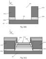
- Figures 3(A) - 3(N) show various manufacturing steps along the same A-A' plane as Figure 2A .
- Figure 3(A) shows a first manufacturing step according to the present invention.
- a silicon-on-insulator wafer is provided, which comprises a silicon substrate 201, on top of which is a buried oxide (e.g. SiO 2 ) layer 302.
- a silicon layer 301 On top of the buried oxide layer is a silicon layer 301, which may be around 1.1 ⁇ m - 1.5 ⁇ m tall (as measured in the y direction from an upper surface of the buried oxide layer to an upper surface of the silicon layer).
- a cavity 303 is etched into the device.
- the cavity extends to an upper surface 304 of the silicon substrate 201 and includes removal of at least a portion of the buried oxide layer, resulting in first 202a and second 202b buried oxide layers located either side of the cavity.
- a portion of the silicon layer is removed and so first 401a and second 401b silicon portions are provided either side of the cavity 303.
- a first precursor optically active stack 310a is epitaxially deposited onto the now etched silicon-on-insulator wafer.
- the epitaxial deposition occurs in n stages, where n corresponds to the number of layers in the precursor optically active stack.
- the precursor optically active stack epitaxially grows from all exposed surfaces. Therefore, not only is there the desirable growth from the upper surface 304 of the silicon substrate, but also from the side walls of the first 401a and second 401b silicon portions and also from the upper surface of these silicon portions. Therefore, facet defects 305a and 305b result which can cause significant signal loss if left in the device. These faceted regions can be understood as resulting from a curvature in each of the layers of the precursor optically active stack.
- the device undergoes a chemical-mechanical planarization process. This removes the portions of the first precursor optically active stack 310a which extend above the cavity formed previously as well as a part of each of the silicon portions 401a and 401b. Around 20 nm of the silicon nitride layer 307 is retained. The planarization process and/or a subsequent etching process are performed so that the height of the first 401a and second 401b silicon portions is around 1 ⁇ m.
- a silicon dioxide hard mask 308 is deposited over the upper surface of the device. The result of this is shown in Figure 3(F) .
- photoresists 309a, 309b, and 309c are provided over the upper surface of the device. Gaps 311a and 311b are provided in the photoresists above the facet defect regions 305a and 305b. Seen from a top-down view, the photoresist would be as a single layer with two rectangular gaps above the respective facet defect regions. This photoresist may be provided by depositing a single layer of photoresist, and then removing the material necessary to form the rectangular gaps e.g. via e-beam r optical photolithography.
- Figure 3(H) shows the result of a subsequent step, where the areas not covered by the photoresist have been etched and the photoresist then removed.
- the depth of this etching step is variable.
- the etching removes around 240 nm of the 400 nm transit buffer, leaving first 242a and second 242b regions of the transit buffer which have a reduced thickness relative to the remaining transit buffer 242.
- the etching removes all of the transit buffer not covered by the photoresist and may etch into the silicon substrate 201.
- the result in this example is a first 201a and second 201b exposed region of the silicon substrate.
- the etching also provides a first channel 312a and second channel 312b which bound two surfaces of the precursor optically active stack.
- the etching depth depends on the thickness of the silicon nitride liner on the bottom of the channel in the next process step, to ensure the top surface of the silicon nitride liner is aligned with the top surface of the BOX layer.
- the first precursor optically active stack 310a and is now a second precursor optically active stack 310b, which is distinguished from the first by no longer including the facet defect regions 305a and 305b.
- the silicon dioxide hard mask 308 is removed and a 240 nm thick silicon nitride (e.g. Si 3 N 4 ) sidewall is deposited on all exposed surfaces of the device.
- a 240 nm thick silicon nitride (e.g. Si 3 N 4 ) sidewall is deposited on all exposed surfaces of the device.
- This is shown in Figure 3(I) , and provides a first 313a, second 313b, and third 313c upper liner (which will be removed) and also the sidewall liners 204a - 204d as well as the first and second bottom liners 204e and 204f, whose top surfaces are aligned with the top surface of the BOX layer, as shown in Figure 2A .
- amorphous silicon also referred to as ⁇ -Si
- First 505a and second 505b bulk filling materials are provided, which will provide the filling material shown in Figure 2A .
- bulk amorphous silicon not contained within the channels 312a and 312b, which should be removed.
- openings 314a - 314c are etched into the amorphous silicon which is not present in the channels 312a and 312b. These openings increase the degree of uniformity obtained during a subsequent chemical-mechanical planarization (CMP) process the result of which is shown in Figure 3(L) .
- CMP chemical-mechanical planarization
- the CMP process is performed so that the upper liner portions 313a - 313c are reduced to around 20nm and the remaining amorphous silicon is substantively aligned with the upper liner portions 313a - 313c.
- a further etching step is performed to bring an uppermost surface of the amorphous silicon into line with an uppermost surface of the second pre-precursor optically active stack. Moreover the upper liner portions 313a - 313c are removed, and so an uppermost surface 230 of the second pre-cursor optically active stack 310b is exposed. After this, a second hard mask 315 is deposited over the uppermost surface.
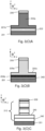
- Figure 3(N) shows a subsequent step from a top-down perspective, omitting the second hard mask 315 for clarity.
- a second photoresist 316 is provided over a central portion of the uppermost surface of the device, extending from one side to the other.
- the width of the second photoresist (measured in the z direction) defines the width of the resulting rib portion of the input waveguide, output waveguide, and optically active stack.
- Figures 3(N)A - 3(N)C show, respectively, cross-sectional views along the lines A-A', B-B', and C-C' in Figure 3(N) .
- Figures 3(O)A - 3(O)C show the input waveguide now comprises the rib portion 203a and slab portion 207a shown in Figure 2B .
- Figure 3(O)B taken along the cross-section B-B' of Figure 3(N) after etching has been performed, shows the filling material now includes a rib portion 205b as well as slab portion 205c which is above the first bottom liner 204e.
- Figure 3(O)C taken along the cross-section C-C' of Figure 3(N) after etching has been performed, shows that the second precursor optically active stack has become the optically active stack 210 shown in Figure 2D .
- the photoresist 316 is removed and bulk silicon dioxide provided to passivate the device.
- steps are shown in Figures 3(P) - 3(Q)A , where one or more electrodes are connected to respective layers of the optically active stack.
- first 601 and second 602 electrode as provided.
- first electrode 601 extends from a position adjacent to the optically active stack (but separated from the transit buffer layer 242 by upper insulating layer 206), up a sidewall of the optically active stack and through a via in the upper insulating layer 206 so as to form an electrical contact with N+ layer 230.
- second electrode 602 extends through a second via in the upper insulting layer 206 to form an electrical contact with the P type buffer layer 240.
- the device When connected to electrodes, the device may be drivable with a voltage of between 0 and 2 V.
- Optical losses of devices according to the present invention are detailed in Table 2 below: Table 2 Driving Voltage (V) Active Length (nm) Active Loss (dB) Si/a-Si Waveguide Mode Mismatch Loss (dB) a-Si/SiGe MQW Waveguide Mode Mismatch Loss (dB) Interface Coupling Loss (dB) Total Loss (dB) Peak ⁇ / ⁇ wavelength (nm) 0-2 80 5.654 0.052 0.229 0.110 6.044 1310 1-3 105 6.217 0.052 0.229 0.110 6.608 1330
Landscapes
- Physics & Mathematics (AREA)
- Nonlinear Science (AREA)
- General Physics & Mathematics (AREA)
- Optics & Photonics (AREA)
- Engineering & Computer Science (AREA)
- Microelectronics & Electronic Packaging (AREA)
- Optical Integrated Circuits (AREA)
- Optical Modulation, Optical Deflection, Nonlinear Optics, Optical Demodulation, Optical Logic Elements (AREA)
Claims (15)
- Siliciumbasierte elektrooptisch aktive Vorrichtung, die Folgendes umfasst:einen Silicium-auf-Isolator-, SOI-, Wellenleiter (250);einen elektrooptisch aktiven Wellenleiter, der einen elektrooptisch aktiven Stapel (210) innerhalb eines Hohlraums des SOI-Wellenleiters umfasst; undeinen ausgekleideten Kanal zwischen dem elektrooptisch aktiven Stapel und dem SOI-Wellenleiter, wobei der ausgekleidete Kanal eine Auskleidung umfasst, die von einer ersten Seitenwandauskleidung (204a), einer zweiten Seitenwandauskleidung (204b) und einer Bodenauskleidung (204e) gebildet wird;wobei der ausgekleidete Kanal mit einem Füllmaterial (205c) gefüllt ist, das einen Brechungsindex aufweist, der jenem eines Materials, das eine Seitenwand des Hohlraums bildet, ähnlich ist, um dadurch einen Brückenwellenleiter im zweiten Kanal zwischen dem SOI-Wellenleiter und dem elektrooptisch aktiven Stapel auszubilden; undwobei die erste Seitenwandauskleidung (204a) zwischen dem Silicium-auf-Isolator-Wellenleiter und dem Füllmaterial angeordnet ist und die zweite Seitenwandauskleidung (204b) zwischen dem Füllmaterial und dem elektrooptisch aktiven Wellenleiter angeordnet ist.
- Siliciumbasierte elektrooptisch aktive Vorrichtung nach Anspruch 1, wobei die Auskleidung aus Siliciumnitrid gebildet ist.
- Siliciumbasierte elektrooptisch aktive Vorrichtung nach Anspruch 1 oder 2, wobei die unterste Oberfläche der Seitenwände des Kanals und die oberste Oberfläche eines Abschnitts der Auskleidung, die in der Basis des Kanals angeordnet ist, mit der obersten Oberfläche einer verdeckten Oxidschicht des SOI fluchtend angeordnet sind.
- Siliciumbasierte elektrooptisch aktive Vorrichtung nach einem der vorangegangenen Ansprüche, wobei die Auskleidung eine Dicke von zumindest 200 nm und nicht mehr als 280 nm aufweist.
- Siliciumbasierte elektrooptisch aktive Vorrichtung nach einem der Ansprüche 1 bis 4, wobei der elektrooptisch aktive Stapel eine Region mit mehreren Quanten-Wells umfasst.
- Siliciumbasierte elektrooptisch aktive Vorrichtung nach einem der vorangegangenen Ansprüche, wobei das Füllmaterial amorphes Silicium oder Siliciumgermanium (SiGe) ist.
- Siliciumbasierte elektrooptisch aktive Vorrichtung nach einem der vorangegangenen Ansprüche, wobei der elektrooptisch aktive Stapel eine Parallelogramm- oder Trapez-Geometrie aufweist.
- Siliciumbasierte elektrooptisch aktive Vorrichtung nach einem der vorangegangenen Ansprüche, die weiters eine epitaktische Mantelschicht umfasst, die zwischen dem Siliciumsubstrat der SOI-Vorrichtung und der optisch aktiven Region, die den elektrooptisch aktiven Wellenleiter bildet, angeordnet ist, wobei die epitaktische Mantelschicht einen Brechungsindex aufweist, der niedriger als jener der Pufferschicht im elektrooptisch aktiven Stapel ist, wobei das epitaktische Material gegebenenfalls Silicium oder Siliciumgermanium (SiGe) ist.
- Verfahren zur Herstellung einer siliciumbasierten elektrooptisch aktiven Vorrichtung, wobei das Verfahren folgende Schritte umfasst:das Bereitstellen eines Silicium-auf-Isolator-, SOI-, Wellenleiters (250);das Ätzen eines Hohlraums in einem Teil des SOI-Wellenleiters durch eine BOX-Schicht des SOI-Wellenleiters hindurch;das epitaxiale Züchten eines elektrooptisch aktiven Stapels innerhalb des Hohlraums und das Ätzen des elektrooptisch aktiven Stapels, um einen elektrooptisch aktiven Wellenleiter (210) auszubilden, wobei der epitaxial gezüchtete, elektrooptisch aktive Stapel eine Facette in einer Region benachbart zu einer Seitenwand des Hohlraums aufweist;das Ätzen der Region, um dadurch die Facette zu entfernen und einen Kanal zwischen der Seitenwand und dem Stapel zu erzeugen;das Auskleiden des Kanals mit einer Auskleidung, um einen ausgekleideten Kanal bereitzustellen, wobei die Auskleidung von einer ersten Seitenwandauskleidung (204a), einer zweiten Seitenwandauskleidung (204b) und einer Bodenauskleidung (204e) gebildet wird;das Füllen des ausgekleideten Kanals mit einem Füllmaterial (205c), das einen Brechungsindex aufweist, der jenem eines Materials, das eine Seitenwand des Hohlraums bildet, ähnlich ist, so dass das Füllmaterial einen Brückenwellenleiter im Kanal zwischen dem SOI-Wellenleiter und dem elektrooptisch aktiven Stapel bildet; undwobei die erste Seitenwandauskleidung (204a) zwischen dem Silicium-auf-Isolator-Wellenleiter und dem Füllmaterial angeordnet ist und die zweite Seitenwandauskleidung (204b) zwischen dem Füllmaterial und dem elektrooptisch aktiven Wellenleiter angeordnet ist.
- Verfahren nach Anspruch 9, wobei der Schritt des Füllens des ausgekleideten Kanals durch plasmaverstärkte chemische Dampfabscheidung oder durch chemische Heißdraht-Dampfabscheidung ausgeführt wird.
- Verfahren nach Anspruch 9 oder 10, das weiters einen Schritt des Abflachens des Füllmaterials durch chemisch-mechanisches Polieren umfasst.
- Verfahren nach einem der Ansprüche 9 bis 11, wobei:
der epitaxial gezüchtete, elektrooptisch aktive Stapel eine zweite Facette in einer zweiten Region benachbart zu der entgegengesetzten Seitenwand des Hohlraums aufweist und wobei der Ätzschritt auch die zweite Region entfernt, um dadurch die zweite Facette zu entfernen und einen zweiten Kanal zwischen der entgegengesetzten Seitenwand und dem Stapel zu erzeugen; wobei im Füllschritt auch der zweite Kanal mit amorphem Silicium gefüllt wird, wobei gegebenenfalls die siliciumbasierte elektrooptisch aktive Vorrichtung ein auf dem Quantenpunkt-beschränkten Stark-Effekt beruhender Elektroabsorptionsmodulator ist. - Verfahren nach einem der Ansprüche 9 bis 12, wobei der epitaxial gezüchtete Stapel eine Pufferschicht umfasst und das Verfahren das Einstellen der Höhe der Pufferschicht auf solche Weise umfasst, dass ein optischer Modus im Modulator an einen optischen Modus im SOI-Wellenleiter angepasst ist.
- Verfahren nach einem der Ansprüche 9 bis 13, wobei der Schritt des Ätzens eines Hohlraums in einem Teil des SOI-Wellenleiters den Schritt des Ätzens des SOI bis zur Basis seiner verdeckten Oxid- (BOX-) Schicht oder darüber hinaus zum Erzeugen einer BOX-losen Region umfasst.
- Verfahren nach Anspruch 14, das weiters den Schritt des Züchtens einer Mantelschicht innerhalb des geätzten Hohlraums umfasst, wobei die Mantelschicht einen Brechungsindex aufweist, der niedriger als der Brechungsindex der Pufferschicht der optisch aktiven Region ist.
Applications Claiming Priority (3)
| Application Number | Priority Date | Filing Date | Title |
|---|---|---|---|
| PCT/EP2017/080221 WO2018096038A1 (en) | 2016-11-23 | 2017-11-23 | Electro-optically active device |
| US201862635955P | 2018-02-27 | 2018-02-27 | |
| PCT/EP2018/062269 WO2019101369A1 (en) | 2017-11-23 | 2018-05-11 | Electro-optically active device |
Publications (3)
| Publication Number | Publication Date |
|---|---|
| EP3714321A1 EP3714321A1 (de) | 2020-09-30 |
| EP3714321B1 true EP3714321B1 (de) | 2023-12-13 |
| EP3714321C0 EP3714321C0 (de) | 2023-12-13 |
Family
ID=66631819
Family Applications (1)
| Application Number | Title | Priority Date | Filing Date |
|---|---|---|---|
| EP18723010.7A Active EP3714321B1 (de) | 2017-11-23 | 2018-05-11 | Elektrooptisch aktive vorrichtung |
Country Status (5)
| Country | Link |
|---|---|
| US (1) | US11126020B2 (de) |
| EP (1) | EP3714321B1 (de) |
| JP (1) | JP7269931B2 (de) |
| CN (1) | CN110168433A (de) |
| WO (1) | WO2019101369A1 (de) |
Families Citing this family (7)
| Publication number | Priority date | Publication date | Assignee | Title |
|---|---|---|---|---|
| GB2573576B (en) * | 2018-05-11 | 2020-06-10 | Rockley Photonics Ltd | Optoelectronic device and method of manufacturing thereof |
| CN112219158A (zh) | 2018-05-15 | 2021-01-12 | 洛克利光子有限公司 | 在soi平台上光子部件的集成 |
| GB2585391B (en) * | 2019-08-23 | 2021-10-27 | Rockley Photonics Ltd | Method of fabricating an optoelectronic component |
| GB2586889B (en) * | 2019-08-26 | 2022-11-02 | Rockley Photonics Ltd | Method of manufacturing a III-V based optoelectronic device |
| US11067749B2 (en) * | 2019-11-21 | 2021-07-20 | Globalfoundries U.S. Inc. | Waveguides with cladding layers of gradated refractive index |
| CN111487791B (zh) * | 2020-04-23 | 2023-12-22 | 济南晶正电子科技有限公司 | 一种集成光学复合基板 |
| JP2022189578A (ja) * | 2021-06-11 | 2022-12-22 | 富士通オプティカルコンポーネンツ株式会社 | 光デバイス及び光通信装置 |
Family Cites Families (86)
| Publication number | Priority date | Publication date | Assignee | Title |
|---|---|---|---|---|
| US5163118A (en) * | 1986-11-10 | 1992-11-10 | The United States Of America As Represented By The Secretary Of The Air Force | Lattice mismatched hetrostructure optical waveguide |
| US6154475A (en) | 1997-12-04 | 2000-11-28 | The United States Of America As Represented By The Secretary Of The Air Force | Silicon-based strain-symmetrized GE-SI quantum lasers |
| JPH11238902A (ja) * | 1998-02-19 | 1999-08-31 | Nec Corp | 半導体光検出装置及び半導体光検出装置の製造方法 |
| US6222951B1 (en) * | 2000-04-03 | 2001-04-24 | Fengyi Huang | Silicon-based silicon-germanium integrated-circuit optical network unit |
| CA2365499C (en) * | 2000-12-26 | 2011-02-15 | National Research Council Of Canada | High speed and high efficiency si-based photodetectors using waveguides formed with silicides for near ir applications |
| US6690863B2 (en) * | 2001-05-17 | 2004-02-10 | Si Optical, Inc. | Waveguide coupler and method for making same |
| US6738546B2 (en) * | 2001-05-17 | 2004-05-18 | Sioptical, Inc. | Optical waveguide circuit including multiple passive optical waveguide devices, and method of making same |
| US6898352B2 (en) * | 2001-05-17 | 2005-05-24 | Sioptical, Inc. | Optical waveguide circuit including passive optical waveguide device combined with active optical waveguide device, and method for making same |
| US6891985B2 (en) * | 2001-05-17 | 2005-05-10 | Sioptical, Inc. | Polyloaded optical waveguide devices and methods for making same |
| US6842546B2 (en) * | 2001-05-17 | 2005-01-11 | Sioptical, Inc. | Polyloaded optical waveguide device in combination with optical coupler, and method for making same |
| US6760498B2 (en) * | 2001-05-17 | 2004-07-06 | Sioptical, Inc. | Arrayed waveguide grating, and method of making same |
| US6967347B2 (en) * | 2001-05-21 | 2005-11-22 | The Regents Of The University Of Colorado | Terahertz interconnect system and applications |
| JP4707885B2 (ja) * | 2001-06-26 | 2011-06-22 | 浜松ホトニクス株式会社 | 光検出素子 |
| JP2006525677A (ja) * | 2003-04-21 | 2006-11-09 | シオプティカル インコーポレーテッド | シリコン・ベースの光デバイスの電子デバイスとのcmos互換集積化 |
| KR100745285B1 (ko) * | 2003-04-23 | 2007-08-01 | 시옵티컬 인코포레이티드 | Soi 광학 플랫폼상에 형성된 서브-마이크론 평면 광파디바이스 |
| JP4847436B2 (ja) * | 2004-02-26 | 2011-12-28 | シオプティカル インコーポレーテッド | シリコン−オン−インシュレータ(soi)構造における光の能動操作 |
| US20050236619A1 (en) * | 2004-04-21 | 2005-10-27 | Vipulkumar Patel | CMOS-compatible integration of silicon-based optical devices with electronic devices |
| US7515777B2 (en) * | 2004-12-09 | 2009-04-07 | The Board Of Trustees Of The Leland Stanford Junior University | Silicon-based Ge/SiGe optical interconnects |
| US8148794B2 (en) * | 2004-12-24 | 2012-04-03 | Google Inc. | Photodetector in germanium on silicon |
| US20060177173A1 (en) * | 2005-02-04 | 2006-08-10 | Sioptical, Inc. | Vertical stacking of multiple integrated circuits including SOI-based optical components |
| WO2007048110A2 (en) * | 2005-10-19 | 2007-04-26 | University Of Notre Dame Du Lac | High-index-contrast waveguide |
| US8160404B2 (en) | 2005-11-22 | 2012-04-17 | Massachusetts Institute Of Technology | High speed and low loss GeSi/Si electro-absorption light modulator and method of fabrication using selective growth |
| US7391801B1 (en) * | 2005-11-25 | 2008-06-24 | The United States Of America As Represented By The Secretary Of The Air Force | Electrically pumped Group IV semiconductor micro-ring laser |
| US8106379B2 (en) * | 2006-04-26 | 2012-01-31 | The Regents Of The University Of California | Hybrid silicon evanescent photodetectors |
| US20080002929A1 (en) * | 2006-06-30 | 2008-01-03 | Bowers John E | Electrically pumped semiconductor evanescent laser |
| US7257283B1 (en) * | 2006-06-30 | 2007-08-14 | Intel Corporation | Transmitter-receiver with integrated modulator array and hybrid bonded multi-wavelength laser array |
| WO2009058470A1 (en) * | 2007-10-30 | 2009-05-07 | Bae Systems Information And Electronic Systems Integration Inc. | Method for fabricating butt-coupled electro-absorptive modulators |
| US8768132B2 (en) | 2008-01-14 | 2014-07-01 | Hewlett-Packard Development Company, L.P. | Ridge waveguide |
| JP5232981B2 (ja) * | 2008-03-07 | 2013-07-10 | 日本電気株式会社 | SiGeフォトダイオード |
| US8330242B2 (en) | 2008-03-28 | 2012-12-11 | Nec Corporation | Semiconductor light-receiving element |
| US8290325B2 (en) * | 2008-06-30 | 2012-10-16 | Intel Corporation | Waveguide photodetector device and manufacturing method thereof |
| JP5387671B2 (ja) * | 2009-03-05 | 2014-01-15 | 富士通株式会社 | 半導体レーザ及び集積素子 |
| US8150223B2 (en) * | 2009-03-31 | 2012-04-03 | Oracle America, Inc. | Thermal tuning of an optical device |
| US8078013B2 (en) * | 2009-03-31 | 2011-12-13 | Oracle America, Inc. | Dual-layer thermally tuned optical device |
| US7848599B2 (en) * | 2009-03-31 | 2010-12-07 | Oracle America, Inc. | Optical device with large thermal impedance |
| US8768170B2 (en) * | 2009-06-29 | 2014-07-01 | Oracle International Corporation | Optical device with reduced thermal tuning energy |
| US9923105B2 (en) * | 2013-10-09 | 2018-03-20 | Skorpios Technologies, Inc. | Processing of a direct-bandgap chip after bonding to a silicon photonic device |
| US9316785B2 (en) * | 2013-10-09 | 2016-04-19 | Skorpios Technologies, Inc. | Integration of an unprocessed, direct-bandgap chip into a silicon photonic device |
| US8340479B2 (en) | 2010-01-14 | 2012-12-25 | Oracle America, Inc. | Electro-optic modulator with inverse tapered waveguides |
| US20110215344A1 (en) * | 2010-03-05 | 2011-09-08 | Dardy Henry D | LOW POWER GRADED BASE SiGe HBT LIGHT MODULATOR |
| US9134553B2 (en) | 2010-03-15 | 2015-09-15 | Agency For Science, Technology And Research | Optical modulator and method for manufacturing the same |
| US8401345B2 (en) * | 2010-06-16 | 2013-03-19 | Oracle America, Inc. | Optical modulator with three-dimensional waveguide tapers |
| US8824837B2 (en) * | 2010-08-26 | 2014-09-02 | The Board Of Trustees Of The Leland Stanford Junior University | Integration of optoelectronics with waveguides using interposer layer |
| US9922967B2 (en) | 2010-12-08 | 2018-03-20 | Skorpios Technologies, Inc. | Multilevel template assisted wafer bonding |
| US9178085B2 (en) * | 2010-12-22 | 2015-11-03 | Bing Li | Waveguide photodetector and forming method thereof |
| WO2012109733A1 (en) * | 2011-02-15 | 2012-08-23 | Luxmux Technology Corporation | A fully integrated complementary metal oxide semiconductor (cmos) fourier transform infrared (ftir) spectrometer and raman spectrometer |
| CN102169243A (zh) * | 2011-04-28 | 2011-08-31 | 中国科学院半导体研究所 | 亚微米波导型Ge量子阱电光调制器 |
| US20120300796A1 (en) * | 2011-05-27 | 2012-11-29 | Sysak Matthew N | Hybrid lasers |
| US8731017B2 (en) * | 2011-08-12 | 2014-05-20 | Acorn Technologies, Inc. | Tensile strained semiconductor photon emission and detection devices and integrated photonics system |
| US9097846B2 (en) * | 2011-08-30 | 2015-08-04 | Skorpios Technologies, Inc. | Integrated waveguide coupler |
| EP2795675A4 (de) * | 2011-12-20 | 2015-11-25 | Intel Corp | Hybride integration von gruppe-iii-v-halbleiterbauelementen auf silicium |
| WO2013095426A1 (en) * | 2011-12-21 | 2013-06-27 | Intel Corporation | Fabrication of planar light-wave circuits (plcs) for optical i/o |
| US8901576B2 (en) * | 2012-01-18 | 2014-12-02 | International Business Machines Corporation | Silicon photonics wafer using standard silicon-on-insulator processes through substrate removal or transfer |
| US9368579B2 (en) | 2012-02-07 | 2016-06-14 | The Board Of Trustees Of The Leland Stanford Junior University | Selective area growth of germanium and silicon-germanium in silicon waveguides for on-chip optical interconnect applications |
| WO2014011846A2 (en) | 2012-07-12 | 2014-01-16 | The Government Of The United States Of America, As Represented By The Secretary Of The Navy | Wavelength and power scalable waveguiding-based infrared laser system |
| US9417186B2 (en) * | 2012-08-30 | 2016-08-16 | Infineon Technologies Ag | Opto-electronic sensor |
| US9219059B2 (en) | 2012-09-26 | 2015-12-22 | International Business Machines Corporation | Semiconductor structure with integrated passive structures |
| WO2014145453A1 (en) * | 2013-03-15 | 2014-09-18 | Gigoptix Inc. | Wavelength tunable integrated optical subassembly based on polymer technology |
| JP6048578B2 (ja) * | 2013-04-19 | 2016-12-21 | 富士通株式会社 | 半導体受光素子及びその製造方法 |
| US9939578B2 (en) * | 2013-05-10 | 2018-04-10 | Intel Corporation | Low cost integration of optical components in planar lightwave circuits |
| US10353224B2 (en) * | 2013-06-09 | 2019-07-16 | Electronic Photonic Ic Inc. (Epic Inc.) | Optical signal processing devices with high device performances |
| CN105593747B (zh) * | 2013-06-09 | 2019-07-05 | 光电网股份有限公司 | 超低电压宽调制带宽低光学损耗光学强度或相位调制器 |
| CN104283093B (zh) * | 2013-07-01 | 2019-07-02 | Imec公司 | 混合波导激光器和用于制造混合波导激光器的方法 |
| WO2015108589A2 (en) * | 2013-10-22 | 2015-07-23 | Massachusetts Institute Of Technology | Waveguide formation using cmos fabrication techniques |
| GB2523383B (en) | 2014-02-24 | 2016-09-14 | Rockley Photonics Ltd | Detector remodulator |
| US10928659B2 (en) * | 2014-02-24 | 2021-02-23 | Rockley Photonics Limited | Optoelectronic device |
| US10663663B2 (en) * | 2014-02-28 | 2020-05-26 | Ciena Corporation | Spot-size converter for optical mode conversion and coupling between two waveguides |
| JP6224495B2 (ja) * | 2014-03-19 | 2017-11-01 | 株式会社東芝 | 半導体レーザ装置 |
| US20180081118A1 (en) * | 2014-07-14 | 2018-03-22 | Biond Photonics Inc. | Photonic integration by flip-chip bonding and spot-size conversion |
| EP3170043A4 (de) * | 2014-07-14 | 2018-06-20 | Biond Photonics Inc. | Photonische 3d-integration mit lichteinkopplungselementen |
| JP5998183B2 (ja) * | 2014-08-27 | 2016-09-28 | 株式会社フジクラ | 基板型光導波路素子 |
| US9209142B1 (en) | 2014-09-05 | 2015-12-08 | Skorpios Technologies, Inc. | Semiconductor bonding with compliant resin and utilizing hydrogen implantation for transfer-wafer removal |
| US9595805B2 (en) | 2014-09-22 | 2017-03-14 | International Business Machines Corporation | III-V photonic integrated circuits on silicon substrate |
| WO2016076793A1 (en) * | 2014-11-10 | 2016-05-19 | Agency for Science,Technology and Research | An optical device and a method for fabricating thereof |
| US9484711B2 (en) * | 2015-01-20 | 2016-11-01 | Sae Magnetics (H.K.) Ltd. | Semiconductor laser apparatus and manufacturing method thereof |
| JP2016152265A (ja) * | 2015-02-16 | 2016-08-22 | 株式会社東芝 | 固体撮像素子 |
| US11150494B2 (en) * | 2015-03-05 | 2021-10-19 | Rockley Photonics Limited | Waveguide modulator structures |
| US9748250B2 (en) * | 2015-06-08 | 2017-08-29 | International Business Machines Corporation | Deep trench sidewall etch stop |
| US10732349B2 (en) * | 2016-02-08 | 2020-08-04 | Skorpios Technologies, Inc. | Broadband back mirror for a III-V chip in silicon photonics |
| US9989831B2 (en) * | 2016-03-02 | 2018-06-05 | The United States Of America, As Represented By The Secretary Of The Navy | Chip-scale two-dimensional optical phased array with simplified controls |
| US20180019139A1 (en) | 2016-07-12 | 2018-01-18 | Ayar Labs, Inc. | Wafer-Level Etching Methods for Planar Photonics Circuits and Devices |
| US11022824B2 (en) | 2016-11-23 | 2021-06-01 | Rockley Photonics Limited | Electro-optically active device |
| US10831043B2 (en) | 2016-11-23 | 2020-11-10 | Rockley Photonics Limited | Electro-optically active device |
| US10340661B2 (en) * | 2017-11-01 | 2019-07-02 | International Business Machines Corporation | Electro-optical device with lateral current injection regions |
| US10355453B2 (en) * | 2017-11-08 | 2019-07-16 | International Business Machines Corporation | Electro-optical device with lateral electron blocking layer |
| GB2573586B (en) | 2017-11-23 | 2020-05-13 | Rockley Photonics Ltd | Electro-optically active device |
-
2018
- 2018-05-11 EP EP18723010.7A patent/EP3714321B1/de active Active
- 2018-05-11 WO PCT/EP2018/062269 patent/WO2019101369A1/en unknown
- 2018-05-11 JP JP2020528381A patent/JP7269931B2/ja active Active
- 2018-05-11 US US16/766,268 patent/US11126020B2/en active Active
- 2018-05-11 CN CN201880002546.7A patent/CN110168433A/zh active Pending
Also Published As
| Publication number | Publication date |
|---|---|
| CN110168433A (zh) | 2019-08-23 |
| JP7269931B2 (ja) | 2023-05-09 |
| EP3714321A1 (de) | 2020-09-30 |
| WO2019101369A1 (en) | 2019-05-31 |
| US11126020B2 (en) | 2021-09-21 |
| EP3714321C0 (de) | 2023-12-13 |
| US20200363662A1 (en) | 2020-11-19 |
| JP2021504747A (ja) | 2021-02-15 |
Similar Documents
| Publication | Publication Date | Title |
|---|---|---|
| EP3714321B1 (de) | Elektrooptisch aktive vorrichtung | |
| US10831043B2 (en) | Electro-optically active device | |
| EP3545356B1 (de) | Elektrooptisch aktive vorrichtung | |
| US10401656B2 (en) | Optoelectronic device | |
| US10216059B2 (en) | Waveguide modulator structures | |
| US10928659B2 (en) | Optoelectronic device | |
| US10838240B2 (en) | Electro-absorption modulator | |
| EP3545357B1 (de) | Optoelektronische vorrichtung | |
| US10921616B2 (en) | Optoelectronic device | |
| US11075498B2 (en) | Method of fabricating an optoelectronic component | |
| US11092825B2 (en) | Optoelectronic device including anti-reflective coatings and method of manufacturing thereof | |
| US10718901B2 (en) | Photonic device having a photonic crystal lower cladding layer provided on a semiconductor substrate | |
| GB2573586A (en) | Electro-optically active device | |
| US20220214498A1 (en) | Photonic chip and method of manufacture | |
| US20220043203A1 (en) | Photonic chip and method of manufacture | |
| CN211480045U (zh) | 电光有源器件 | |
| WO2019220207A1 (en) | lll-V/SI HYBRID OPTOELECTRONIC DEVICE AND METHOD OF MANUFACTURE | |
| CN116249921A (zh) | 波导结构 |
Legal Events
| Date | Code | Title | Description |
|---|---|---|---|
| STAA | Information on the status of an ep patent application or granted ep patent |
Free format text: STATUS: UNKNOWN |
|
| STAA | Information on the status of an ep patent application or granted ep patent |
Free format text: STATUS: THE INTERNATIONAL PUBLICATION HAS BEEN MADE |
|
| PUAI | Public reference made under article 153(3) epc to a published international application that has entered the european phase |
Free format text: ORIGINAL CODE: 0009012 |
|
| STAA | Information on the status of an ep patent application or granted ep patent |
Free format text: STATUS: REQUEST FOR EXAMINATION WAS MADE |
|
| 17P | Request for examination filed |
Effective date: 20200623 |
|
| AK | Designated contracting states |
Kind code of ref document: A1 Designated state(s): AL AT BE BG CH CY CZ DE DK EE ES FI FR GB GR HR HU IE IS IT LI LT LU LV MC MK MT NL NO PL PT RO RS SE SI SK SM TR |
|
| AX | Request for extension of the european patent |
Extension state: BA ME |
|
| DAV | Request for validation of the european patent (deleted) | ||
| DAX | Request for extension of the european patent (deleted) | ||
| STAA | Information on the status of an ep patent application or granted ep patent |
Free format text: STATUS: EXAMINATION IS IN PROGRESS |
|
| 17Q | First examination report despatched |
Effective date: 20220104 |
|
| 111Z | Information provided on other rights and legal means of execution |
Free format text: AL AT BE BG CH CY CZ DE DK EE ES FI FR GB GR HR HU IE IS IT LT LU LV MC MK MT NL NO PL PT RO RS SE SI SK SM TR Effective date: 20221215 |
|
| GRAP | Despatch of communication of intention to grant a patent |
Free format text: ORIGINAL CODE: EPIDOSNIGR1 |
|
| STAA | Information on the status of an ep patent application or granted ep patent |
Free format text: STATUS: GRANT OF PATENT IS INTENDED |
|
| INTG | Intention to grant announced |
Effective date: 20230426 |
|
| D11X | Information provided on other rights and legal means of execution (deleted) | ||
| GRAS | Grant fee paid |
Free format text: ORIGINAL CODE: EPIDOSNIGR3 |
|
| RAP3 | Party data changed (applicant data changed or rights of an application transferred) |
Owner name: ROCKLEY PHOTONICS LIMITED |
|
| RIN1 | Information on inventor provided before grant (corrected) |
Inventor name: ZILKIE, AARON Inventor name: ZHANG, YI Inventor name: YU, GUOMIN |
|
| 111Z | Information provided on other rights and legal means of execution |
Free format text: AL AT BE BG CH CY CZ DE DK EE ES FI FR GB GR HR HU IE IS IT LT LU LV MC MK MT NL NO PL PT RO RS SE SI SK SM TR Effective date: 20230815 |
|
| GRAA | (expected) grant |
Free format text: ORIGINAL CODE: 0009210 |
|
| STAA | Information on the status of an ep patent application or granted ep patent |
Free format text: STATUS: THE PATENT HAS BEEN GRANTED |
|
| AK | Designated contracting states |
Kind code of ref document: B1 Designated state(s): AL AT BE BG CH CY CZ DE DK EE ES FI FR GB GR HR HU IE IS IT LI LT LU LV MC MK MT NL NO PL PT RO RS SE SI SK SM TR |
|
| REG | Reference to a national code |
Ref country code: GB Ref legal event code: FG4D |
|
| REG | Reference to a national code |
Ref country code: CH Ref legal event code: EP |
|
| REG | Reference to a national code |
Ref country code: DE Ref legal event code: R096 Ref document number: 602018062563 Country of ref document: DE |
|
| REG | Reference to a national code |
Ref country code: IE Ref legal event code: FG4D |
|
| U01 | Request for unitary effect filed |
Effective date: 20240109 |
|
| U07 | Unitary effect registered |
Designated state(s): AT BE BG DE DK EE FI FR IT LT LU LV MT NL PT SE SI Effective date: 20240117 |
|
| PG25 | Lapsed in a contracting state [announced via postgrant information from national office to epo] |
Ref country code: GR Free format text: LAPSE BECAUSE OF FAILURE TO SUBMIT A TRANSLATION OF THE DESCRIPTION OR TO PAY THE FEE WITHIN THE PRESCRIBED TIME-LIMIT Effective date: 20240314 |
|
| PG25 | Lapsed in a contracting state [announced via postgrant information from national office to epo] |
Ref country code: ES Free format text: LAPSE BECAUSE OF FAILURE TO SUBMIT A TRANSLATION OF THE DESCRIPTION OR TO PAY THE FEE WITHIN THE PRESCRIBED TIME-LIMIT Effective date: 20231213 |
|
| PG25 | Lapsed in a contracting state [announced via postgrant information from national office to epo] |
Ref country code: GR Free format text: LAPSE BECAUSE OF FAILURE TO SUBMIT A TRANSLATION OF THE DESCRIPTION OR TO PAY THE FEE WITHIN THE PRESCRIBED TIME-LIMIT Effective date: 20240314 Ref country code: ES Free format text: LAPSE BECAUSE OF FAILURE TO SUBMIT A TRANSLATION OF THE DESCRIPTION OR TO PAY THE FEE WITHIN THE PRESCRIBED TIME-LIMIT Effective date: 20231213 |