EP3709364A1 - Lichtemittierende diodeneinheit für eine anzeige mit mehreren pixeln und anzeigevorrichtung damit - Google Patents
Lichtemittierende diodeneinheit für eine anzeige mit mehreren pixeln und anzeigevorrichtung damit Download PDFInfo
- Publication number
- EP3709364A1 EP3709364A1 EP17931562.7A EP17931562A EP3709364A1 EP 3709364 A1 EP3709364 A1 EP 3709364A1 EP 17931562 A EP17931562 A EP 17931562A EP 3709364 A1 EP3709364 A1 EP 3709364A1
- Authority
- EP
- European Patent Office
- Prior art keywords
- light emitting
- light
- wavelength converter
- display
- wavelength
- Prior art date
- Legal status (The legal status is an assumption and is not a legal conclusion. Google has not performed a legal analysis and makes no representation as to the accuracy of the status listed.)
- Pending
Links
Images





Classifications
-
- H—ELECTRICITY
- H10—SEMICONDUCTOR DEVICES; ELECTRIC SOLID-STATE DEVICES NOT OTHERWISE PROVIDED FOR
- H10H—INORGANIC LIGHT-EMITTING SEMICONDUCTOR DEVICES HAVING POTENTIAL BARRIERS
- H10H29/00—Integrated devices, or assemblies of multiple devices, comprising at least one light-emitting semiconductor element covered by group H10H20/00
- H10H29/10—Integrated devices comprising at least one light-emitting semiconductor component covered by group H10H20/00
- H10H29/14—Integrated devices comprising at least one light-emitting semiconductor component covered by group H10H20/00 comprising multiple light-emitting semiconductor components
- H10H29/142—Two-dimensional arrangements, e.g. asymmetric LED layout
-
- H—ELECTRICITY
- H10—SEMICONDUCTOR DEVICES; ELECTRIC SOLID-STATE DEVICES NOT OTHERWISE PROVIDED FOR
- H10H—INORGANIC LIGHT-EMITTING SEMICONDUCTOR DEVICES HAVING POTENTIAL BARRIERS
- H10H20/00—Individual inorganic light-emitting semiconductor devices having potential barriers, e.g. light-emitting diodes [LED]
- H10H20/80—Constructional details
- H10H20/83—Electrodes
-
- H—ELECTRICITY
- H10—SEMICONDUCTOR DEVICES; ELECTRIC SOLID-STATE DEVICES NOT OTHERWISE PROVIDED FOR
- H10H—INORGANIC LIGHT-EMITTING SEMICONDUCTOR DEVICES HAVING POTENTIAL BARRIERS
- H10H20/00—Individual inorganic light-emitting semiconductor devices having potential barriers, e.g. light-emitting diodes [LED]
- H10H20/80—Constructional details
- H10H20/85—Packages
- H10H20/851—Wavelength conversion means
-
- H—ELECTRICITY
- H10—SEMICONDUCTOR DEVICES; ELECTRIC SOLID-STATE DEVICES NOT OTHERWISE PROVIDED FOR
- H10H—INORGANIC LIGHT-EMITTING SEMICONDUCTOR DEVICES HAVING POTENTIAL BARRIERS
- H10H29/00—Integrated devices, or assemblies of multiple devices, comprising at least one light-emitting semiconductor element covered by group H10H20/00
- H10H29/30—Active-matrix LED displays
- H10H29/34—Active-matrix LED displays characterised by the geometry or arrangement of subpixels within a pixel, e.g. relative disposition of the RGB subpixels
- H10H29/345—Active-matrix LED displays characterised by the geometry or arrangement of subpixels within a pixel, e.g. relative disposition of the RGB subpixels the area of the subpixels being different
-
- H—ELECTRICITY
- H10—SEMICONDUCTOR DEVICES; ELECTRIC SOLID-STATE DEVICES NOT OTHERWISE PROVIDED FOR
- H10H—INORGANIC LIGHT-EMITTING SEMICONDUCTOR DEVICES HAVING POTENTIAL BARRIERS
- H10H29/00—Integrated devices, or assemblies of multiple devices, comprising at least one light-emitting semiconductor element covered by group H10H20/00
- H10H29/80—Constructional details
- H10H29/85—Packages
- H10H29/851—Wavelength conversion means
- H10H29/8511—Wavelength conversion means characterised by their material, e.g. binder
- H10H29/8512—Wavelength conversion materials
- H10H29/8513—Wavelength conversion materials having two or more wavelength conversion materials
-
- H—ELECTRICITY
- H10—SEMICONDUCTOR DEVICES; ELECTRIC SOLID-STATE DEVICES NOT OTHERWISE PROVIDED FOR
- H10H—INORGANIC LIGHT-EMITTING SEMICONDUCTOR DEVICES HAVING POTENTIAL BARRIERS
- H10H29/00—Integrated devices, or assemblies of multiple devices, comprising at least one light-emitting semiconductor element covered by group H10H20/00
- H10H29/80—Constructional details
- H10H29/85—Packages
- H10H29/851—Wavelength conversion means
- H10H29/8514—Wavelength conversion means characterised by their shape, e.g. plate or foil
-
- H—ELECTRICITY
- H10—SEMICONDUCTOR DEVICES; ELECTRIC SOLID-STATE DEVICES NOT OTHERWISE PROVIDED FOR
- H10H—INORGANIC LIGHT-EMITTING SEMICONDUCTOR DEVICES HAVING POTENTIAL BARRIERS
- H10H29/00—Integrated devices, or assemblies of multiple devices, comprising at least one light-emitting semiconductor element covered by group H10H20/00
- H10H29/80—Constructional details
- H10H29/85—Packages
- H10H29/851—Wavelength conversion means
- H10H29/8515—Wavelength conversion means not being in contact with the bodies
-
- H—ELECTRICITY
- H10—SEMICONDUCTOR DEVICES; ELECTRIC SOLID-STATE DEVICES NOT OTHERWISE PROVIDED FOR
- H10W—GENERIC PACKAGES, INTERCONNECTIONS, CONNECTORS OR OTHER CONSTRUCTIONAL DETAILS OF DEVICES COVERED BY CLASS H10
- H10W90/00—Package configurations
-
- H—ELECTRICITY
- H10—SEMICONDUCTOR DEVICES; ELECTRIC SOLID-STATE DEVICES NOT OTHERWISE PROVIDED FOR
- H10H—INORGANIC LIGHT-EMITTING SEMICONDUCTOR DEVICES HAVING POTENTIAL BARRIERS
- H10H29/00—Integrated devices, or assemblies of multiple devices, comprising at least one light-emitting semiconductor element covered by group H10H20/00
- H10H29/30—Active-matrix LED displays
- H10H29/49—Interconnections, e.g. wiring lines or terminals
-
- H—ELECTRICITY
- H10—SEMICONDUCTOR DEVICES; ELECTRIC SOLID-STATE DEVICES NOT OTHERWISE PROVIDED FOR
- H10H—INORGANIC LIGHT-EMITTING SEMICONDUCTOR DEVICES HAVING POTENTIAL BARRIERS
- H10H29/00—Integrated devices, or assemblies of multiple devices, comprising at least one light-emitting semiconductor element covered by group H10H20/00
- H10H29/80—Constructional details
- H10H29/832—Electrodes
- H10H29/8321—Electrodes characterised by their shape
-
- H—ELECTRICITY
- H10—SEMICONDUCTOR DEVICES; ELECTRIC SOLID-STATE DEVICES NOT OTHERWISE PROVIDED FOR
- H10H—INORGANIC LIGHT-EMITTING SEMICONDUCTOR DEVICES HAVING POTENTIAL BARRIERS
- H10H29/00—Integrated devices, or assemblies of multiple devices, comprising at least one light-emitting semiconductor element covered by group H10H20/00
- H10H29/80—Constructional details
- H10H29/832—Electrodes
- H10H29/8322—Electrodes characterised by their materials
- H10H29/8325—Reflective materials
-
- H—ELECTRICITY
- H10—SEMICONDUCTOR DEVICES; ELECTRIC SOLID-STATE DEVICES NOT OTHERWISE PROVIDED FOR
- H10H—INORGANIC LIGHT-EMITTING SEMICONDUCTOR DEVICES HAVING POTENTIAL BARRIERS
- H10H29/00—Integrated devices, or assemblies of multiple devices, comprising at least one light-emitting semiconductor element covered by group H10H20/00
- H10H29/80—Constructional details
- H10H29/842—Coatings, e.g. passivation layers or antireflective coatings
Definitions
- Exemplary embodiments relate to a light emitting diode for a next-generation display and a display apparatus having the same.
- light emitting diodes As an inorganic light source, light emitting diodes have been used in various technical fields, such as displays, vehicular lamps, general lighting, and the like. With various advantages of the light emitting diodes, such as longer lifespan, lower power consumption, and faster response, than existing light sources, light emitting diodes have been replacing the existing light sources.
- a display apparatus displays various colors through mixture of blue, green, and red light.
- Each pixel of the display apparatus includes blue, green, and red sub-pixels, in which a color of a certain pixel is determined based on the colors of the sub-pixels, and an image is realized through a combination of such pixels.
- micro LEDs are disposed at respecitve sub-pixels, and accordingly, a large number of micro LEDs need to be arranged on a single substrate.
- a micro LED is extremely small, which is 200 ⁇ m or less, and further 100 ⁇ m or less, and these small sizes cause various problems. In particular, it is difficult to handle the light emitting diode having a small size, and it is also difficult to replace a failed LED from mounted micro LEDs with a good-quality LED.
- the light emitting diode generally emits ultraviolet or blue light, and can be combined with a phosphor to realize green light and red light.
- a color filter is used for each sub-pixel to improve the purity of each color, and each of color filters has a difference in filter efficiency. Accordingly, even if the same light emitting diode is operated to emit light of the same intensity, differences in the light intensity of the blue sub-pixel, the green sub-pixel, and the red sub-pixel occur. To overcome the differences, an operating current density of each light emitting diode may be changed, but a decrease in light emitting efficiency of the light emitting diode may occur due to the change in current density.
- Exemplary embodiments provide a light emitting diode for a display that is easy to be mounted and replaced and a display apparatus having the same.
- Exemplary embodiments provide a light emitting diode for a display that is capable of operating light emitting diodes of each sub-pixel under an optimum light emission efficiency condition and a display apparatus having the same.
- An LED unit for a display includes a plurality of pixels.
- Each of the pixels includes: a first light emitting cell, a second light emitting cell, and a third light emitting cell, each of the first, second, and third light emitting cells including a first conductivity type semiconductor layer, an active layer, and a second conductivity type semiconductor layer; pads electrically connected to the first, second, and third light emitting cells to independently drive the first, second, and third light emitting cells; a second wavelength converter that converts a wavelength of light emitted from the second light emitting cell; and a third wavelength converter that converts a wavelength of light emitted from the third light emitting cell, in which the third wavelength converter converts a wavelength of light to a longer wavelength than a wavelength of light converted by the second wavelength converter, the second light emitting cell has a larger area than that of the first light emitting cell, and the third light emitting cell has a larger area than that of the second light emitting cell.
- a display apparatus includes: a circuit board; and a plurality of LED units arranged on the circuit board, in which each of the plurality of LED units is the LED unit for a display according to the exemplary embodiment above.
- a plurality of pixels that includes sub-pixels including a first, second, and third light emitting cells and emitting light of different colors is disposed in one LED unit, and thus, an LED unit for a display that may be easy to be mounted and replaced is provided. Furthermore, by varying areas of the first, second, and third light emitting cells, light emitting cells of each of the sub-pixels may be driven under an optimum light emission efficiency condition.
- An LED unit for a display includes a plurality of pixels.
- Each of the pixels includes: a first light emitting cell, a second light emitting cell, and a third light emitting cell, each of the first, second, and third light emitting cells including a first conductivity type semiconductor layer, an active layer, and a second conductivity type semiconductor layer; pads electrically connected to the first, second, and third light emitting cells to independently drive the first, second, and third light emitting cells; a second wavelength converter that converts a wavelength of light emitted from the second light emitting cell; and a third wavelength converter that converts a wavelength of light emitted from the third light emitting cell, in which the third wavelength converter converts a wavelength of light to a longer wavelength than a wavelength of light converted by the second wavelength converter, the second light emitting cell has a larger area than that of the first light emitting cell, and the third light emitting cell has a larger area than that of the second light emitting cell.
- a plurality of pixels is disposed in one LED unit and three light emitting cells are disposed in each of the pixels to realize light of different colors in each pixel.
- a plurality of pixels that includes three sub-pixels may be formed using one LED unit. Accordingly, a size of the LED unit is relatively increased compared to that of the conventional micro LED, and thus, it may be easy to mount and replace the LED unit. Further, areas of the light emitting cells are set to be different from one another by considering a conversion efficiency of a wavelength converter and the like, and thus, the light emitting cells may be driven under an optimum light emission efficiency condition.
- LED unit refers to a unit of a light emitting diode mounted on a circuit board. Pixels in one LED unit are physically connected to one another so that the pixels in the LED unit are mounted or replaced together. Therefore, the pixels in one LED unit are not separately used. Accordingly, one LED unit includes an element that connects internal pixels to one another, and the element is spaced apart from another LED unit.
- the first, second, and third light emitting cells may emit blue light
- the second wavelength converter may convert the blue light into green light
- the third wavelength converter may convert the blue light into red light. Blue light emitted from the first light emitting cell is used without wavelength conversion.
- Area ratios of the second light emitting cell and the third light emitting cell to the first light emitting cell may be set in consideration of a light conversion efficiency of the second wavelength converter and a light conversion efficiency of the third wavelength converter, respectively.
- the area of the light emitting cell becomes larger.
- the area ratios of the second light emitting cell and the third light emitting cell to the first light emitting cell may be inversely proportional to the light conversion efficiency of the second wavelength converter and the light conversion efficiency of the third wavelength converter, respectively.
- the LED unit for a display may further include a first wavelength converter that converts a wavelength of light emitted from the first light emitting cell to light of a first wavelength, in which the first wavelength converter may convert a wavelength of light to a shorter wavelength than a wavelength of light converted by the second wavelength converter, and the first, second, and third light emitting cells may emit ultraviolet light.
- the first wavelength converter may convert ultraviolet light into blue light
- the second wavelength converter may convert the ultraviolet light into green light
- the third wavelength converter may convert the ultraviolet light into red light
- Area ratios of the second light emitting cell and the third light emitting cell to the first light emitting cell may be set in consideration of light conversion efficiencies of the first wavelength converter, the second wavelength converter, and the third wavelength converter.
- the area ratios of the second light emitting cell and the third light emitting cell to the first light emitting cell may be inversely proportional to a light conversion efficiency ratio of the second wavelength converter to the first wavelength converter and a light conversion efficiency ratio of the third wavelength converter to the first wavelength converter, respectively.
- the LED unit for a display may further include a second color filter disposed on the second wavelength converter; and a third color filter disposed on the third wavelength converter.
- the second color filter may filter light other than green light
- the third color filter may filter light other than red light.
- the light emitting diode for a display may further include a first color filter disposed on the first wavelength converter, and the first color filter filters light other than blue light.
- Area ratios of the first light emitting cell, the second light emitting cell, and the third light emitting cell may be 1: 2: 7.
- the first, second, and third light emitting cells of each pixel may share a first conductivity type semiconductor layer. Further, at least two pixels may share the first conductivity type semiconductor layer. The light emitting cells or pixels may share the first conductivity type semiconductor layer, thereby providing an LED unit having a simple manufacturing process and structure.
- At least one pad may be commonly electrically connected to the first conductivity type semiconductor layer or the second conductivity type semiconductor layer of the first, second, and third light emitting cells. As such, the number of pads that are required may be reduced.
- the LED unit for a display may further include: ohmic reflection layers disposed on the second conductivity type semiconductor layers of the first, second, and third light emitting cells; a lower insulation layer covering the first, second, and third light emitting cells of the plurality of pixels and including at least one first opening exposing a first conductivity type semiconductor layer and second openings exposing the ohmic reflection layers.
- the LED unit for a display may further include: a first pad electrode disposed on the lower insulation layer and electrically connected to the first conductivity type semiconductor layer through the first opening of the lower insulation layer; a second pad electrode spaced apart from the first pad electrode to be disposed on the lower insulation layer and electrically connected to the ohmic reflection layer through the second opening; and an upper insulation layer covering the first and second pad electrodes, in which the pads may be connected to the first and second pad electrodes through openings of the upper insulation layer.
- the lower insulation layer may include a distributed Bragg reflector.
- the lower insulation layer may cover side surfaces of the light emitting cells, and thus, light interference between the light emitting cells may be prevented.
- the pads may include one first pad that are commonly connected to the first conductivity type semiconductor layers of the first, second, and third light emitting cells and three second pads that are connected to the second conductivity type semiconductor layers of the first, second, and third light emitting cells, respectively.
- the one first pad may be commonly connected to first conductivity type semiconductor layers of at least two pixels.
- the pads may include first pads connected to the first conductivity type semiconductor layers of the first, second, and third light emitting cells, respectively, and one second pad commonly connected to the second conductivity type semiconductor layers of the first, second, and third light emitting cells.
- the one second pad may be commonly connected to second conductivity type semiconductor layers of at least two pixels.
- a display apparatus includes: a circuit board; and a plurality of LED units arranged on the circuit board, in which each of the plurality of LED units is the LED unit for a display according to the exemplary embodiment above.
- the first, second, and third light emitting cells may further be driven in a passive matrix or active matrix manner.
- FIG. 1 is a schematic cross-sectional view illustrating a display apparatus according to an exemplary embodiment
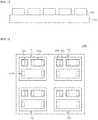
- FIG. 2 is a schematic plan view illustrating an LED unit for a display according to an exemplary embodiment
- FIG. 3 is an enlarged plan view of a pixel in the LED unit for a display of FIG. 2
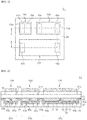
- FIG. 4 is a schematic cross-sectional view taken along the line A-A of FIG. 3 .
- the display apparatus includes a circuit board 100 and an LED unit 200 for a display.
- a plurality of LED units 200 is disposed on the circuit board 100, the inventive concepts are not necessarily limited thereto, and a single LED unit 200 may be disposed on the circuit board 100.
- the circuit board 100 includes a circuit for driving light emitting cells in the LED unit 200 in a passive matrix or active matrix manner.
- the circuit board 100 may be a printed circuit board including passive devices such as resistors.
- the circuit board 100 may include active devices such as thin film transistors.
- the LED unit 200 for a display includes a plurality of pixels F1, F2, F3, and F4 as shown in FIG. 2 .
- four pixels are shown, but the inventive concepts are not limited thereto, and the number of pixels disposed in one LED unit 200 may be two or three, or may be five or more.
- Each of the pixel F1, F2, F3 or F4 includes three light emitting cells, and wavelength converters are disposed on each of the light emitting cells to realize blue, green, and red light. Structures of the pixels F1, F2, F3, and F4 are generally the same or similar.
- the pixel F1 as a representative will be described in detail with reference to FIG. 3 and FIG. 4 .
- the pixel F1 may include a substrate 21, first, second, and third light emitting cells 30 (30a, 30b, 30c), an ohmic reflection layer 31, and a lower insulation layer 33, first and second pad electrodes 35a and 35b, an upper insulation layer 37, a first wavelength converter 51a, a second wavelength converter 51b, a third wavelength converter 51c, a first color filter 53a, a second color filter 53b, a third color filter 53c, and a light blocking material layer 55( or a partition wall).
- Each of the first, second, and third light emitting cells 30a, 30b, and 30c includes a first conductivity type semiconductor layer 23, an active layer 25, and a second conductivity type semiconductor layer 27.
- the pixel F1 also include sub-pixels 10B, 10G, and 10R, where each of the sub-pixels 10B, 10G, and 10R includes the light emitting cell 30, the wavelength converters 51a, 51b, and 51c, and the filters 53a, 53b, and 53c.
- the substrate 21 is not particularly limited as long as it is a substrate capable of growing a gallium nitride-based semiconductor layer.
- the substrate 21 may be various, such as a sapphire substrate, a gallium nitride substrate, a SiC substrate, and the substrate 21 may be a patterned sapphire substrate.
- a plurality of pixels F1, F2, F3, and F4 may be provided on one substrate 21, and the substrate 21 may have a rectangular or square shape, but the inventive concepts are not necessarily limited thereto.
- An overall size of the substrate 21 may vary depending on the number of pixels.
- the first, second, and third light emitting cells 30a, 30b, and 30c are disposed to be spaced apart from one another.
- An interval between the light emitting cells in the pixel F1 may be smaller than that between the pixels F1, F2, F3, and F4, but may be the same.
- the first, second, and third light emitting cells 30a, 30b, and 30c have different areas from one another.
- the second light emitting cell 30b has a larger area than that of the first light emitting cell 30a
- the third light emitting cell 30c has a larger area than that of the second light emitting cell 30b.
- Areas of the first, second, and third light emitting cells 30a, 30b, and 30c may be determined in consideration of light conversion efficiencies of the wavelength converters 51a, 51b, and 51c, which will be described later.
- the first, second, and third light emitting cells 30a, 30b, and 30c may be disposed adjacent to one another. More particularly, the first light emitting cell 30a may be adjacent to the second and third light emitting cells 30b and 30c, the second light emitting cell 30b may be adjacent to the first and third light emitting cells 30a and 30c, and the third light emitting cell 30c may be adjacent to the first light emitting cell and the second light emitting cell 30a and 30b. As shown in FIG. 3 , the first and second light emitting cells 30a and 30b may be arranged along the long axis of the third light emitting cell 30c. However, the inventive concepts are not limited thereto, and may be variously arranged in other forms.
- one light emitting cell may be disposed between two remaining light emitting cells.
- the first, second, and third light emitting cells 30a, 30b, and 30c may have a rectangular shape, but the inventive concepts are not limited thereto, and may have various shapes.
- Each of the first, second, and third light emitting cells 30a, 30b, and 30c includes the first conductivity type semiconductor layer 23, the active layer 25, and the second conductivity type semiconductor layer 27.
- the first conductivity type semiconductor layer 23 is disposed under the substrate 21.
- the first conductivity type semiconductor layer 23 is a layer grown on the substrate 21 and may be a gallium nitride-based semiconductor layer doped with impurities, such as Si.
- the active layer 25 and the second conductivity type semiconductor layer 27 are disposed on the first conductivity type semiconductor layer 23.
- the active layer 25 is disposed between the first conductivity type semiconductor layer 23 and the second conductivity type semiconductor layer 27.
- the active layer 25 and the second conductivity type semiconductor layer 27 may have a smaller area than that of the first conductivity type semiconductor layer 23.
- the active layer 25 and the second conductivity type semiconductor layer 27 may be partially removed to expose a portion of the first conductivity type semiconductor layer 23. As shown in FIG. 4 , a through hole may be formed through the active layer 25 and the second conductivity type semiconductor layer 27 to expose the first conductivity type semiconductor layer 23.
- the active layer 25 and the second conductivity type semiconductor layer 27 may be formed in a mesa shape, and the first conductivity type semiconductor layer 23 around the mesa may be exposed.
- the active layer 25 may have a single quantum well structure or multiple quantum well structure.
- a composition and thickness of the well layer in the active layer 25 determines a wavelength of light that is generated.
- the active layers 25 of the first light emitting cell 30a, the second light emitting cell 30b, and the third light emitting cell 30c are all grown on the same substrate 21 under the same conditions and have substantially the same composition and thickness, thereby emitting light of the same wavelength.
- the second conductivity type semiconductor layer 27 may be a gallium nitride-based semiconductor layer doped with a p-type impurity, for example Mg.
- Each of the first conductivity type semiconductor layer 23 and the second conductivity type semiconductor layer 27 may be a single layer, but the inventive concepts are not limited thereto, and may be a multiple layer or may include a superlattice layer.
- the first conductivity type semiconductor layer 23, the active layer 25, and the second conductivity type semiconductor layer 27 may be formed by growing on the substrate 21 in a chamber using a known method such as metal organic chemical vapor deposition (MOCVD) or molecular beam epitaxy (MBE).
- MOCVD metal organic chemical vapor deposition
- MBE molecular beam epitaxy
- the ohmic reflection layer 31 is in ohmic contact with the second conductivity type semiconductor layer 27 of each of the light emitting cell 30a, 30b, and 30c.
- the ohmic reflection layer 31 may include an ohmic layer such as Ni or ITO and a reflection layer such as Ag or Al.
- the ohmic reflection layer 31 may also include a transparent oxide layer such as ITO and an insulation layer such as SiO 2 between the reflection layers, and the reflection layer may connect to the transparent oxide layer through an insulation layer.
- the lower insulation layer 33 covers the light emitting cells 30a, 30b, and 30c, and covers side surfaces of the exposed second conductivity type semiconductor layer 27 and the active layer 25.
- the lower insulation layer 33 has openings exposing the first conductivity type semiconductor layer 23 and the ohmic reflection layer 31.
- the lower insulation layer 33 may include a single layer such as SiO 2 or Si 3 N 4 , but the inventive concepts are not limited thereto, and may include multiple layers.
- the lower insulation layer 33 may include a distributed Bragg reflector.
- the first pad electrode 35a and the second pad electrode 35b are disposed on the lower insulation layer 33.
- the first pad electrode 35a and the second pad electrode 35b are disposed on each light emitting cell, the first pad electrode 35a is electrically connected to the first conductivity type semiconductor layer 23, and the second electrode pad 35b is electrically connected to the ohmic reflection layer 31.
- the first pad electrode 35a and the second pad electrode 35b may be formed together in the same process, and thus, may be located at substantially the same level.
- the second pad electrode 35b may be omitted.
- the first pad electrode 35a may be disposed to surround the second pad electrode 35b.
- the pad electrodes 35a and 35b of one sub-pixel may be spaced apart from the pad electrodes 35a and 35b of an adjacent sub-pixel.
- the first, second, and third light emitting cells 30a, 30b, and 30c in the LED unit 200 are electrically spaced apart from one another.
- the pad electrodes 35a and 35b in the pixel F1 are also spaced apart from the pad electrodes 35a and 35b in the other pixels F2, F3, and F4.
- inventive concepts are not limited thereto, and various embodiments in which the light emitting cells 30a, 30b, and 30c are electrically connected to one another are possible, and various embodiments in which the light emitting cells are electrically connected between pixels are possible. This will be described in detail in other embodiments.
- the upper insulation layer 37 covers the first and second pad electrodes 35a and 35b, and has openings exposing the first and second pad electrodes 35a and 35b.
- the upper insulation layer 37 may include a single layer such as SiO 2 or Si 3 N 4 , but the inventive concepts are not limited thereto, and may include multiple layers.
- the lower insulation layer 33 may include a distributed Bragg reflector.
- first and second bump pads 43a and 43b are formed on each of the light emitting cell 30a, 30b, and 30c, and connected to the first and second pad electrodes 35a and 35b through the openings of the upper insulation layer 37. More particularly, the first bump pad 43a is connected to the first pad electrode 35a, and the second bump pad 43b is connected to the second pad electrode 35b. Two bump pads 43a and 43b are provided for each of the light emitting cell 30a, 30b, and 30c.
- the bump pads 43a and 43b occupy a relatively large area, and maximum widths of the bump pads 43a and 43b may exceed at least 1/2 of a minimum width of the light emitting cell.
- the bump pads 43a and 43b may have a rectangular shape as illustrated, but are not limited thereto, and may have a circular or elliptical shape.
- the bump pads 43a and 43b may be used to mount the LED unit 200 on the circuit board 100, and may include Au or AuSn, for example.
- a dummy bump pad (not shown) in addition to the bump pads 43a and 43b, may be disposed on at least one light emitting cell. Since the light emitting cells have different areas, the dummy bump pad may be disposed on the light emitting cells 30b or 30c that has a relatively large area. The dummy bump pad may be disposed on the upper insulation layer 37 to be electrically isolated from the bump pads 43a and 43b. The dummy bump pad may be used as a heat dissipation path for dissipating heat generated from light emitting cells, thereby improving light efficiency of the LED unit 200.
- a support member 45 may cover side surfaces of the bump pads 43a and 43b.
- the support member 45 may also cover side surfaces of the dummy bump pad.
- the support member 45 may include a thermosetting or thermoplastic resin.
- the first, second, and third wavelength converters 51a, 51b, and 51c are disposed on the substrate 21 facing the light emitting cells 30a, 30b, and 30c.
- the first wavelength converter 51a is disposed on the first light emitting cell 30a
- the second wavelength converter 51b is disposed on the second light emitting cell 30b
- the third wavelength converter 51c is disposed the third light emitting cell 30c.
- the first wavelength converter 51a converts a wavelength of light emitted from the first light emitting cell 30a
- the second wavelength converter 51b converts a wavelength of light emitted from the second light emitting cell 30b
- the third wavelength converter 51c converts a wavelength of light emitted from the third light emitting cell 30c.
- the second wavelength converter 51b converts light to a longer wavelength than a wavelength of light converted by the first wavelength converter 51a
- the third wavelength converter 51c converts light to a longer wavelength than a wavelength of light converted by the second wavelength converter 51b.
- the first, second, and third light emitting cells 30a, 30b, and 30c may emit ultraviolet light
- the first wavelength converter 51a converts ultraviolet light into blue light
- the second wavelength converter 51b converts ultraviolet light into green light
- the third wavelength converter 51c may convert ultraviolet light into red light.
- the first color filter 53a, the second color filter 53b, and the third color filter 53c are disposed on the first, second, and third wavelength converters 51a, 51b, and 51c, respectively, and filter light emitted therefrom.
- the first color filter 53a filters light other than blue light
- the second color filter 53b filters light other than green light
- the third color filter 53c filters light other than red light.
- the active layer 25 may emit blue light.
- the first wavelength converter 51a may be omitted, and a transparent resin may be disposed in place of the first wavelength converter 51a.
- the second wavelength converter 51b converts blue light into green light
- the third wavelength converter 51c converts blue light into red light.
- the light blocking material layer 55 may be disposed between the wavelength converters 51a, 51b, and 51c.
- the light blocking material layer 55 blocks light from progressing from one wavelength converter to another wavelength converter, thereby preventing light interference between the sub-pixels 10B, 10G, and 10R.
- the light blocking material layer 55 may include white resin or PSR that is capable of reflecting light.
- the lower insulation layer 33 may include the distributed Bragg reflector, or the first pad electrode 35a and/or the second pad electrode 35b may be disposed to cover sidewalls of the light emitting cells, and thus, light interference between the light emitting cells 30a, 30b, and 30c is prevented.
- the pixel F1 of the exemplary embodiment has three sub-pixels 10B, 10G, and 10R, and the sub-pixels are fixed on the substrate 21.
- the sub-pixel 10B may realize blue light by the light emitting cell 10a or by a combination of the first light emitting cell 10a and the first wavelength converter 51a
- the sub-pixel 10G may realize green light by a combination of the light emitting cell 10b and the second wavelength converter 51b
- the sub-pixel 10R may realize red light by a combination of the third light emitting cell 10c and the third wavelength converter 51c.
- the pixels F2, F3, and F3 include sub-pixels having substantially the same structure as that of the pixel F1. Further, the substrate 21, the lower insulation layer 33, and the upper insulation layer 37 may be continuously formed over all of the pixels F1, F2, F3, and F4.
- the LED unit 200 having flip-type light emitting cells, and thus, it is possible to improve light emission efficiency of each light emitting cell.
- a plurality of pixels F1, F2, F3, and F4 together with the substrate 21 may be mounted on the circuit board 100.
- the conventional micro LED since individual sub-pixels are mounted, the number of processes is large and it is difficult to perform the mounting process.
- one LED unit includes the plurality of pixels F1, F2, F3, and F4, a size of the LED unit is relatively larger than that of the conventional micro LED, and thus, the number of mounting processes is reduced, and the mounting becomes easy.
- the first, second, and third light emitting cells 30a, 30b, and 30c in the exemplary embodiment have different areas from one another.
- the wavelength converters 51a, 51b, and 51c disposed on the light emitting cells have different areas from one another.
- a relative area of the light emitting cells may be closely related to light conversion efficiencies of the wavelength converters, and may also be related to color filtering efficiencies of the color filters 53a, 53b, and 53c.
- the wavelength converters may generally include phosphors.
- beta sialon SiAlON
- CASN CaAlSiN-based phosphor
- phosphors cannot convert all blue light into green light or red light, and each phosphor has a constant light conversion efficiency.
- a red phosphor that converts ultraviolet or blue light of the same wavelength into red light has a smaller light conversion efficiency than that of a green phosphor that converts into light green light.
- red light also has lower visibility than green light. Therefore, when the first, second, and third light emitting cells 30a, 30b, and 30c are formed to have the same area, the third light emitting cell 30c of the subpixel 10R that realizes red light has to be driven under a higher current density to realize a sensitivity similar to that of other sub-pixels 10B or 10G.
- the second light emitting cell 30b of the sub-pixel 10G that realizes green light also has to be driven under a higher current density than that of the first light emitting cell 30a. More particularly, there is a difference in current density required for realizing an image for each light emitting cell, and accordingly, there is a problem that it is impossible to drive the first, second, and third light emitting cells 30a, 30b, and 30c under an optimal light emission efficiency condition.
- the light emitting cells are provided with substantially the same or similar current density for driving the light emitting cells by varying the areas of the first, second, and third light emitting cells 30a, 30b, and 30c, and thus, the light emitting cells may be driven under the optimum light emission efficiency condition.
- the relative areas of the first, second, and third light emitting cells 30a, 30b, and 30c may be determined in consideration of the relative light conversion efficiency of the first, second, and third wavelength converters 51a, 51b, and 51c. As the light conversion efficiency of the wavelength converter becomes smaller, the area of the corresponding light emitting cell is set to be larger.
- the first wavelength converter 51a when the first, second, and third light emitting cells 30a, 30b, and 30c emit blue light, the first wavelength converter 51a is omitted, and area ratios of the second light emitting cell 30b and the third light emitting cell 30c to the first light emitting cell 30a may be inversely proportional to the light conversion efficiency of the second wavelength converter 51b and the light conversion efficiency of the third wavelength converter 51c, respectively.
- the second wavelength converter 51b includes beta sialon and the third wavelength converter 51c includes CASN
- relative areas ratios of the first light emitting cell 30a, the second light emitting cell 30b, and the third light emitting cell 30c may be 1: 2: 7.
- the area ratio of the second light emitting cell 30b and the third light emitting cell 30c relative to the first light emitting cell 30a may be inversely proportional to the light conversion efficiency ratio of the second wavelength converter 51b to the first wavelength converter 51a and the light conversion efficiency ratio of the third wavelength converter 51c to the first wavelength converter 51a, respectively.
- the area of the light emitting cells is determined in consideration of the light conversion efficiencies of the wavelength converters in the exemplary embodiment, when filtering efficiencies of the first, second, and third color filters 53a, 53b, and 53c are different from one another, it is also possible to determine the areas of the light emitting cells in consideration of the difference in the filtering efficiencies.
- the areas of the first, second, and third light emitting cells 30a, 30b, and 30c are set to be different from one another, and thus, the light emitting cells may be driven under substantially the same current density.
- the current density may be set with the optimal condition for driving the light emitting cells, thereby improving light emission efficiency.
- FIG. 5 is a schematic cross-sectional view of a pixel illustrating an LED unit for a display according to another exemplary embodiment.
- the LED unit according to the exemplary embodiment is substantially similar to the LED unit described with reference to FIG. 3 and FIG. 4 , but the substrate 21 is omitted.
- First, second, and third wavelength converters 51a, 51b, and 51c are disposed on light emitting cells 30a, 30b, and 30c instead of being disposed on the substrate 21.
- the substrate 21 may be removed using a technique such as laser lift-off or the like, or roughness may be formed on a surface of an exposed first conductivity type semiconductor layer 23.
- the substrate 21 since the substrate 21 is removed, light interference that may be generated between adjacent sub-pixels and between adjacent pixels F1, F2, F3, and F4 caused by light transmitted in the lateral direction through the substrate 21 may be further suppressed.
- FIG. 6 is a schematic circuit diagram illustrating a driving manner of a display apparatus according to an exemplary embodiment.
- a region indicated by the bold line represents a pixel that has three light emitting cells.
- a plurality of LED units may be arranged on the circuit board 100 of FIG. 1 , and accordingly, light emitting cells may be arranged in a matrix form.
- Pixels F1, F2, F3, and F4 in one LED unit 200 may be connected to a scan line and a data line as shown in FIG. 6 .
- the scan line and the data line may be provided in the circuit board 100, and pads 35a and 35b may be bonded on the circuit board 100 to form a circuit as shown in FIG. 6 .
- anodes of three light emitting cells in the pixel F1 and three light emitting cells in the pixel F3 are commonly connected to a data line Vdata1, and cathodes thereof are connected to scan lines Vscan1, Vscan2, Vscan3, Vscan4, Vscan5, and Vscan6 that are different from one another.
- Anodes of three light emitting cells in the pixel F2 and three light emitting cells in the pixel F4 are commonly connected to a data line Vdata2, and cathodes thereof are connected to the scan lines Vscan1, Vscan2, Vscan3, Vscan4, Vscan5, and Vscan6 that are different from one another.
- the cathode of each light emitting cell of the pixel F1 is connected to the same scanning line together with the cathode of each light emitting cell of the pixel F2.
- a sub-pixel that emits light may be selected by the scan line and the data line, and images may be realized by sequentially selecting sub-pixels. Also, light intensity emitted from one sub-pixel may be adjusted by using a pulse width modulation (PWM) method or by changing a voltage (or current) between the data line and the scan line.
- PWM pulse width modulation
- FIG. 7 is a schematic circuit diagram illustrating a driving manner of a display apparatus according to another exemplary embodiment.
- pixels F1, F2, F3, and F4 in an LED unit are arranged in a matrix form in a driving circuit.
- FIG. 8 is a schematic circuit diagram illustrating a driving manner of a display apparatus according to another exemplary embodiment.
- the pixels F1, F2, F3, and F4 in the exemplary embodiments of FIG. 6 and FIG. 7 are arranged in a matrix form in the driving circuit, but anodes of all light emitting cells in the exemplary embodiment are connected to the same data line.
- Pixels F1, F2, F3, and F4 may be arranged in a matrix form on the substrate 21, but a circuit as shown in FIG. 8 may also be formed through electrical connection between the pixels F1, F2, F3, and F4 and a circuit board 100.
- FIG. 9 is a schematic circuit diagram illustrating a driving manner of a display apparatus according to another exemplary embodiment.
- the anodes of all light emitting cells of the pixels F1, F2, F3, and F4 in the embodiment of FIG. 8 are connected to the same data line, but anodes of all light emitting cells in the exemplary embodiment are connected to different data lines from one another within a drive circuit, and cathodes thereof are connected to the same scan line.
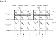
- FIG. 10 is a schematic circuit diagram illustrating a driving manner of a display apparatus according to another exemplary embodiment.
- the previous exemplary embodiments are for the passive matrix driving manner, while the present embodiment is for the active matrix driving manner.
- a driving circuit includes two or more transistors Tr1 and Tr2 and a capacitor.
- Tr1 and Tr2 When the power is connected to selection lines Vrow1, Vrow2, and Vrow3 and a data voltage is applied to data lines Vdata1, Vdata2, and Vdata3, voltages are applied to corresponding light emitting cells of LED1, LED2, or LED3.
- charges are charged in the corresponding capacitors according to values of Vdata1, Vdata2, and Vdata3. Since turn-on state of Tr2 may be maintained by the charging voltage of the capacitor, the voltage of the capacitor may be maintained and the voltage may be applied to the light emitting cells of LED 1, LED2, and LED3 even when the Vrow1 is powered off. Further, the current flowing through LED1, LED2, and LED3 may be changed according to the values of Vdata1, Vdata2, and Vdata3. Current may always be supplied through common current supplies Vdd, and thus, continuous light emission is possible.
- the transistors Tr1 and Tr2 and the capacitors may be formed in a circuit board 100.
- a thin film transistor formed on a silicon substrate may be used for active matrix driving.
- Anodes of the light emitting cells are connected to the transistor Tr2 and cathodes thereof are grounded.
- the anodes of the light emitting cells are connected to different transistors Tr2 from one another and the cathodes thereof are grounded, the anodes of a plurality of light emitting cells may be connected to the same common current supply Vdd, and the cathodes thereof may be connected to different transistors from one another.
- the anodes or cathodes of the light emitting cells may be commonly electrically connected.
- the first, second, and third light emitting cells 30a, 30b, and 30c of the LED unit 200 described above are electrically separated from one another in the LED unit 200, and are electrically connected to one another through the circuit board 100.
- some or all of the light emitting cells in the LED unit 200 may be electrically connected to one another in the LED unit, and electrical connection thereof will be described below.
- FIG. 11 is a schematic cross-sectional view of a pixel F1 in an LED unit for a display according to another exemplary embodiment.
- the pixel F1 according to the exemplary embodiment is substantially similar to that described with reference to FIG. 4 , but first conductivity type semiconductor layers 23 of the light emitting cells 30a, 30b, and 30c in the exemplary embodiment are connected to one another by a first electrode pad 35a.
- a single first electrode pad 35a is formed over the light emitting cells 30a, 30b, and 30c, and electrically connected to the first conductivity type semiconductor layers 23 in each region of the light emitting cells 30a, 30b, and 30c . Accordingly, cathodes of the light emitting cells 30a, 30b, and 30c are electrically connected to one another.
- first conductivity type semiconductor layers 23 of the light emitting cells 30a, 30b, and 30c are connected to one another by the first electrode pad 35a, it may not be necessary to dispose bump pads 43a on the respective light emitting cells, and current may be supplied to each of the light emitting cells 30a, 30b, and 30c using a single bump pad 43a.
- the cathodes of the light emitting cells in at least two of the pixels F1, F2, F3, and F4 may be connected to one another by the first electrode pad 35a, and accordingly, the number of bump pads 43a required in the LED unit 200 may be further reduced.
- light emitting cells 30a, 30b, and 30c are disposed under the substrate 21 in the illustrated exemplary embodiment, the substrate 21 may be omitted as described with reference to FIG. 5 .
- FIG. 12 is a schematic cross-sectional view of a pixel in an LED unit for a display according to another exemplary embodiment.
- the first conductivity type semiconductor layers 23 of the light emitting cells 30a, 30b, and 30c in the embodiment of FIG. 11 are electrically connected using the first electrode pad 35a
- light emitting cells 30a, 30b, and 30c in the exemplary embodiment share a first conductivity type semiconductor layer 23.
- the first conductivity type semiconductor layers 23 are spaced apart from one another, and the first electrode pad 35a electrically connects the first conductivity type semiconductor layers 23 in the embodiment of FIG. 11 , but, since the light emitting cells 30a, 30b, and 30c in the exemplary embodiment share the first conductivity type semiconductor layer 23, a first electrode pad 35a in the exemplary embodiment may be connected to the first conductivity type semiconductor layer 23 anywhere.
- the first electrode pad 35a may be connected to the first conductivity type semiconductor layer 23 through a through hole as shown in FIG. 11 , or the first electrode pad 35a may be connected to the first conductivity type semiconductor layer 23 in a region between the light emitting cells 30a, 30b, and 30c or a region around the light emitting cells 30a, 30b, and 30c as shown in FIG. 12 .
- connection regions of the first electrode pad 35a may be selected variously, and thus, light emitting areas of the light emitting cells 30a, 30b, and 30c may be increased within a limited area of the LED unit 200 .
- Pixels F1, F2, F3, and F4 may also share the first conductivity type semiconductor layer 23, which will be described in detail later with reference to FIGS. 14 through 17 .
- light emitting cells 30a, 30b, and 30c are disposed under the substrate 21 in the exemplary embodiment, the substrate 21 may be omitted as described with reference to FIG. 5 .
- FIG. 13 is a schematic cross-sectional view of a pixel F1 in an LED unit for a display according to another exemplary embodiment.
- the cathodes of the light emitting cells 30a, 30b, and 30c are electrically connected to one another, but anodes of the light emitting cells 30a, 30b, and 30c in the exemplary embodiment are electrically connected to one another.
- a second conductivity type semiconductor layers 27 of the light emitting cells 30a, 30b, and 30c are electrically connected to one another by a second electrode pad 35b.
- first conductivity type semiconductor layers 23 of the light emitting cells 30a, 30b, and 30c are electrically separated from one another.
- the second electrode pad 35b may be continuously formed on the first, second, and third light emitting cells 30a, 30b, and 30c, and electrically connected to ohmic reflection layers 31 on each light emitting cell.
- the second electrode pad 35b in the exemplary embodiment may also surround first electrode pads 35a.
- bump pads 43b do not need to be disposed on each light emitting cell, and current may be supplied to each of the light emitting cells 30a, 30b, and 30c using a single bump pad 43b.
- Anodes of the light emitting cells in at least two of the pixels F1, F2, F3, and F4 may be connected to one another by the second electrode pad 35b, and accordingly, the number of bump pads 43b required in the LED unit 200 may be further reduced.
- the substrate 21 may be omitted as described with reference to FIG. 5 .
- FIG. 14 is a schematic plan view illustrating an LED unit for a display according to another exemplary embodiment.
- light emitting cells 30a, 30b, and 30c in each pixel F1, F2, F3, or F4 may share a first conductivity type semiconductor layer 23.
- the first conductivity type semiconductor layers may be spaced apart from one another between the pixels.
- a circuit for connecting the light emitting cells may not need to be provided in a circuit board 100, and the number of bump pads 43a may also be reduced. More particularly, one bump pad 43a and three bump pads 43b may be disposed for each pixel.
- the cathodes of the light emitting cells in the same pixel will be connected to the same data line or scan line.
- the cathodes of the light emitting cells in the same pixel will be grounded.
- the pixels F1, F2, F3, and F4 are electrically separated from one another, the pixels may be variously arranged in the driving circuit.
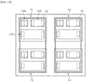
- FIG. 15 is a schematic plan view illustrating an LED unit for a display according to another exemplary embodiment.
- a pixel F1 and a pixel F3 share a first conductivity type semiconductor layer 23, and a pixel F2 and a pixel F4 also share the first conductivity type semiconductor layer 23. Accordingly, a bump pad 43a that is common to the pixels F1 and F3 may be disposed, and a bump pad 43a that is common to the pixels F2 and F4 may be disposed, and thus, the number of the bump pads 43a may be further reduced compared to the exemplary embodiment 14.
- cathodes of light emitting cells in the pixel F1 and the pixel F3 will all be connected to the same data line or scan line, and those of light emitting cells in the pixel F2 and the pixel F4 will be connected to the same data line or scan line.
- the cathodes of the light emitting cells in the pixels F1, F2, F3, and F4 will be grounded.
- FIG. 16 is a schematic plan view illustrating an LED unit for a display according to another exemplary embodiment.
- pixels F1 and F2 share a first conductivity type semiconductor layer 23, and pixels F3 and F4 also share the first conductivity type semiconductor layer 23 in the exemplary embodiment. Accordingly, a bump pad 43a that is common to the pixels F1 and F2 may be disposed, and a bump pad 43a that is common to the pixels F3 and F4 may be disposed, and thus, the number of the bump pads 43a may be further reduced compared to the exemplary embodiment 14.
- cathodes of light emitting cells in the pixel F1 and the pixel F2 will all be connected to the same data line or scan line, and those of light emitting cells in the pixel F3 and the pixel F4 will be connected to the same data line or scan line.
- the cathodes of the light emitting cells in the pixels F1, F2, F3, and F4 will be grounded.
- FIG. 17 is a schematic plan view illustrating an LED unit for a display according to another exemplary embodiment.
- all pixels F1, F2, F3, and F4 in the LED unit 200 may share a first conductivity type semiconductor layer 23. Accordingly, a bump pad 43a that is common to the pixels F1, F2, F3, and F4 may be disposed, further reducing the number of bump pads 43a compared to the embodiments of FIG. 15 and FIG. 16 .
- FIG. 18A and FIG. 18B are cross-sectional views illustrating a film including a wavelength converter.
- the first, second, and third wavelength converters 51a, 51b, and 51c in the above embodiments may be spaced apart from one another to be individually attached or formed on light emitting cells 30a, 30b, and 30c, but first, second, and third wavelength converters 51a, 51b, and 51c in the exemplary embodiment are arranged in one layer in one film.
- a transparent or opaque resin 151 may be disposed in a region between the wavelength converters 51a, 51b, and 51c.
- the opaque resin 151 may function as a light blocking layer 55.
- the first wavelength converter 51a may be omitted, and in this case, the transparent resin 151 may be disposed at a location where the first wavelength converter 51a is disposed.
- a film including wavelength converters 51a, 51b, and 51c may be disposed on each pixel, or one film may cover two or more pixels.
- the film according to the exemplary embodiment is a multi-layer laminated film.
- a first layer 151a may include the first wavelength converter 51a
- a second layer 151b may include the second wavelength converter 51b
- a third layer 151c may include the third wavelength converter 51c.
- the first, second, and third layers 151a, 151b, and 151c may be composed of a combination of the transparent resin 151 and the wavelength converters 51a, 51b, and 51c, respectively.
- the first layer 151a may be omitted.
- the laminated film may be disposed on each pixel, or a single laminated film may cover a plurality of pixels.
- films having various structures may be used.
Landscapes
- Led Device Packages (AREA)
- Led Devices (AREA)
- Devices For Indicating Variable Information By Combining Individual Elements (AREA)
Applications Claiming Priority (1)
| Application Number | Priority Date | Filing Date | Title |
|---|---|---|---|
| PCT/KR2017/012558 WO2019093533A1 (ko) | 2017-11-08 | 2017-11-08 | 복수의 픽셀들을 포함하는 디스플레이용 발광 다이오드 유닛 및 그것을 갖는 디스플레이 장치 |
Publications (2)
| Publication Number | Publication Date |
|---|---|
| EP3709364A1 true EP3709364A1 (de) | 2020-09-16 |
| EP3709364A4 EP3709364A4 (de) | 2021-06-23 |
Family
ID=66438938
Family Applications (1)
| Application Number | Title | Priority Date | Filing Date |
|---|---|---|---|
| EP17931562.7A Pending EP3709364A4 (de) | 2017-11-08 | 2017-11-08 | Lichtemittierende diodeneinheit für eine anzeige mit mehreren pixeln und anzeigevorrichtung damit |
Country Status (7)
| Country | Link |
|---|---|
| US (5) | US11121172B2 (de) |
| EP (1) | EP3709364A4 (de) |
| JP (1) | JP7222993B2 (de) |
| KR (1) | KR102565147B1 (de) |
| CN (2) | CN110121781B (de) |
| BR (1) | BR112020009088B1 (de) |
| WO (1) | WO2019093533A1 (de) |
Cited By (2)
| Publication number | Priority date | Publication date | Assignee | Title |
|---|---|---|---|---|
| EP3690944A4 (de) * | 2017-09-29 | 2021-06-16 | Seoul Semiconductor Co., Ltd. | Lichtemittierende vorrichtung und anzeigevorrichtung damit |
| WO2025003052A1 (en) * | 2023-06-27 | 2025-01-02 | Signify Holding B.V. | Lighting arrangement |
Families Citing this family (27)
| Publication number | Priority date | Publication date | Assignee | Title |
|---|---|---|---|---|
| KR20250090372A (ko) | 2016-03-24 | 2025-06-19 | 소니그룹주식회사 | 발광 장치, 표시 장치 및 조명 장치 |
| TWI707491B (zh) * | 2019-12-04 | 2020-10-11 | 錼創顯示科技股份有限公司 | 微型發光二極體顯示面板 |
| CN108828841B (zh) * | 2018-07-26 | 2021-01-15 | 武汉华星光电技术有限公司 | Led背光装置及led显示装置 |
| US11688710B2 (en) * | 2019-03-25 | 2023-06-27 | Innolux Corporation | Electronic device |
| US11282893B2 (en) * | 2019-07-29 | 2022-03-22 | Beijing Xiaomi Mobile Software Co., Ltd. Nanjing Branch | Display panel, display screen, and electronic device |
| TWI717871B (zh) * | 2019-10-22 | 2021-02-01 | 友達光電股份有限公司 | 顯示裝置 |
| US11489002B2 (en) * | 2019-10-29 | 2022-11-01 | Seoul Viosys Co., Ltd. | LED display apparatus |
| CN113871373A (zh) * | 2020-06-11 | 2021-12-31 | 群创光电股份有限公司 | 发光装置 |
| CN111812888A (zh) * | 2020-07-10 | 2020-10-23 | 深圳市华星光电半导体显示技术有限公司 | Mini LED背光模组及其制备方法、显示面板 |
| US11527572B2 (en) | 2020-08-05 | 2022-12-13 | Jade Bird Display (shanghai) Limited | Scan needle and scan display system including same |
| US11270620B2 (en) | 2020-08-05 | 2022-03-08 | Jade Bird Display (shanghai) Limited | Scan needle and scan display system including same |
| US11270632B2 (en) * | 2020-08-05 | 2022-03-08 | Jade Bird Display (shanghai) Limited | Scan needle and scan display system including same |
| US11308848B2 (en) * | 2020-08-05 | 2022-04-19 | Jade Bird Display (shanghai) Limited | Scan needle and scan display system including same |
| US11317065B2 (en) | 2020-08-05 | 2022-04-26 | Jade Bird Display (shanghai) Limited | Scan needle and scan display system including same |
| US11308862B2 (en) * | 2020-08-05 | 2022-04-19 | Jade Bird Display (shanghai) Limited | Scan needle and scan display system including same |
| CN112117297A (zh) * | 2020-10-22 | 2020-12-22 | 中国科学院长春光学精密机械与物理研究所 | 全彩色Micro LED阵列结构及其制备方法 |
| US12610858B2 (en) | 2021-05-14 | 2026-04-21 | Seoul Viosys Co., Ltd. | Light emitting module and display apparatus having the same |
| CN115483323A (zh) * | 2021-05-31 | 2022-12-16 | 京东方科技集团股份有限公司 | 发光器件、发光基板和发光器件的制作方法 |
| CN115692452A (zh) * | 2021-07-26 | 2023-02-03 | 重庆康佳光电技术研究院有限公司 | 显示面板及其制作方法 |
| KR102887715B1 (ko) * | 2021-08-10 | 2025-11-18 | 삼성디스플레이 주식회사 | 표시 장치 |
| JP7233128B1 (ja) * | 2021-12-21 | 2023-03-06 | ナイトライド・セミコンダクター株式会社 | マイクロledディスプレイ及びその製造方法 |
| CN117096246A (zh) * | 2022-05-12 | 2023-11-21 | 华为技术有限公司 | 微发光二极管显示屏及制备方法 |
| CN120358862A (zh) * | 2022-06-30 | 2025-07-22 | 湖北长江新型显示产业创新中心有限公司 | 一种显示面板、显示装置及制备方法 |
| CN115394216B (zh) * | 2022-10-20 | 2023-07-14 | 季华实验室 | 一种显示装置和显示设备 |
| CN115483327B (zh) * | 2022-11-09 | 2023-03-24 | 镭昱光电科技(苏州)有限公司 | Micro LED微显示芯片及其制造方法 |
| KR20240103491A (ko) * | 2022-12-27 | 2024-07-04 | 엘지디스플레이 주식회사 | 표시 장치 및 표시 장치의 제조 방법 |
| US20250169247A1 (en) * | 2023-11-20 | 2025-05-22 | Lumileds Llc | Led with segmented semiconductor structure |
Family Cites Families (28)
| Publication number | Priority date | Publication date | Assignee | Title |
|---|---|---|---|---|
| JP3589187B2 (ja) | 2000-07-31 | 2004-11-17 | 日亜化学工業株式会社 | 発光装置の形成方法 |
| JP2002217545A (ja) | 2001-01-18 | 2002-08-02 | Kyocera Corp | 多層配線基板 |
| JP2002217454A (ja) | 2001-01-19 | 2002-08-02 | Matsushita Electric Ind Co Ltd | Ledアレー及びこれを用いたled表示装置 |
| TWI466266B (zh) * | 2009-02-24 | 2014-12-21 | 晶元光電股份有限公司 | 陣列式發光元件及其裝置 |
| KR101601624B1 (ko) | 2010-02-19 | 2016-03-09 | 삼성전자주식회사 | 멀티셀 어레이를 갖는 반도체 발광장치, 발광모듈 및 조명장치 |
| KR20110098600A (ko) | 2010-02-26 | 2011-09-01 | 삼성엘이디 주식회사 | 멀티셀 어레이를 갖는 반도체 발광장치 및 이의 제조방법 |
| EP2367203A1 (de) * | 2010-02-26 | 2011-09-21 | Samsung LED Co., Ltd. | Licht emittierende Halbleitervorrichtung mit Matrix mehrerer Zellen und Verfahren zu deren Herstellung |
| KR101761834B1 (ko) | 2011-01-28 | 2017-07-27 | 서울바이오시스 주식회사 | 웨이퍼 레벨 발광 다이오드 패키지 및 그것을 제조하는 방법 |
| KR101476207B1 (ko) * | 2012-06-08 | 2014-12-24 | 엘지전자 주식회사 | 반도체 발광 소자를 이용한 디스플레이 장치 |
| KR101422037B1 (ko) | 2012-09-04 | 2014-07-23 | 엘지전자 주식회사 | 반도체 발광 소자를 이용한 디스플레이 장치 |
| KR20140083488A (ko) * | 2012-12-26 | 2014-07-04 | 엘지전자 주식회사 | 반도체 발광 소자를 이용한 디스플레이 장치 |
| KR102087935B1 (ko) * | 2012-12-27 | 2020-03-11 | 엘지이노텍 주식회사 | 발광 소자 |
| US9111464B2 (en) * | 2013-06-18 | 2015-08-18 | LuxVue Technology Corporation | LED display with wavelength conversion layer |
| KR102098245B1 (ko) | 2014-02-11 | 2020-04-07 | 삼성전자 주식회사 | 광원 패키지 및 그를 포함하는 표시 장치 |
| JP6612119B2 (ja) | 2015-02-16 | 2019-11-27 | 株式会社東芝 | 半導体発光装置 |
| JP2016218151A (ja) | 2015-05-15 | 2016-12-22 | シャープ株式会社 | 波長変換基板、発光装置並びにこれを備えた表示装置、照明装置および電子機器 |
| DE102015108532A1 (de) | 2015-05-29 | 2016-12-01 | Osram Opto Semiconductors Gmbh | Anzeigevorrichtung mit einer Mehrzahl getrennt voneinander betreibbarer Bildpunkte |
| US10259831B2 (en) | 2015-07-29 | 2019-04-16 | California Institute Of Technology | Hydroxide-catalyzed formation of silicon-oxygen bonds by dehydrogenative coupling of hydrosilanes and alcohols |
| KR102342556B1 (ko) | 2015-07-31 | 2021-12-23 | 엘지전자 주식회사 | 반도체 발광 소자를 이용한 디스플레이 장치 |
| WO2017034379A1 (ko) | 2015-08-26 | 2017-03-02 | 엘지전자 주식회사 | 반도체 발광소자의 이송 헤드, 이송 시스템 및 반도체 발광소자를 이송하는 방법 |
| KR102465382B1 (ko) * | 2015-08-31 | 2022-11-10 | 삼성디스플레이 주식회사 | 표시장치 및 표시장치의 제조방법 |
| KR102524805B1 (ko) * | 2016-02-12 | 2023-04-25 | 삼성전자주식회사 | 광원 모듈, 디스플레이 패널 및 이를 구비한 디스플레이 장치 |
| KR102455084B1 (ko) | 2016-02-23 | 2022-10-14 | 쑤저우 레킨 세미컨덕터 컴퍼니 리미티드 | 발광소자 패키지 및 이를 갖는 표시장치 |
| KR102462658B1 (ko) * | 2016-03-18 | 2022-11-03 | 엘지이노텍 주식회사 | 발광소자 및 이를 포함하는 표시장치 |
| KR102480220B1 (ko) * | 2016-04-08 | 2022-12-26 | 삼성전자주식회사 | 발광 다이오드 모듈 및 이를 구비한 디스플레이 패널 |
| KR101873505B1 (ko) * | 2017-08-30 | 2018-07-02 | 서울반도체 주식회사 | 웨이퍼 레벨 발광 다이오드 패키지 |
| KR102650950B1 (ko) | 2017-09-29 | 2024-03-26 | 서울반도체 주식회사 | 발광 소자 및 그것을 갖는 표시 장치 |
| WO2019066491A1 (ko) | 2017-09-29 | 2019-04-04 | 서울반도체 주식회사 | 발광 소자 및 그것을 갖는 표시 장치 |
-
2017
- 2017-11-08 CN CN201780081450.XA patent/CN110121781B/zh active Active
- 2017-11-08 US US16/762,357 patent/US11121172B2/en active Active
- 2017-11-08 KR KR1020207008006A patent/KR102565147B1/ko active Active
- 2017-11-08 CN CN202410143447.8A patent/CN117976691A/zh active Pending
- 2017-11-08 WO PCT/KR2017/012558 patent/WO2019093533A1/ko not_active Ceased
- 2017-11-08 EP EP17931562.7A patent/EP3709364A4/de active Pending
- 2017-11-08 JP JP2020524640A patent/JP7222993B2/ja active Active
- 2017-11-08 BR BR112020009088-3A patent/BR112020009088B1/pt active IP Right Grant
-
2021
- 2021-08-16 US US17/403,793 patent/US11764253B2/en active Active
-
2023
- 2023-08-15 US US18/234,271 patent/US12009385B2/en active Active
-
2024
- 2024-05-08 US US18/658,378 patent/US12310161B2/en active Active
-
2025
- 2025-04-03 US US19/169,221 patent/US20250261491A1/en active Pending
Cited By (5)
| Publication number | Priority date | Publication date | Assignee | Title |
|---|---|---|---|---|
| EP3690944A4 (de) * | 2017-09-29 | 2021-06-16 | Seoul Semiconductor Co., Ltd. | Lichtemittierende vorrichtung und anzeigevorrichtung damit |
| US11641008B2 (en) | 2017-09-29 | 2023-05-02 | Seoul Viosys Co., Ltd. | Light emitting device and display apparatus including the same |
| US11824145B2 (en) | 2017-09-29 | 2023-11-21 | Seoul Viosys Co., Ltd. | Light emitting device and display apparatus including the same |
| US12527133B2 (en) | 2017-09-29 | 2026-01-13 | Seoul Viosys Co., Ltd. | Light emitting device and display apparatus including the same |
| WO2025003052A1 (en) * | 2023-06-27 | 2025-01-02 | Signify Holding B.V. | Lighting arrangement |
Also Published As
| Publication number | Publication date |
|---|---|
| JP2021511528A (ja) | 2021-05-06 |
| KR20200070228A (ko) | 2020-06-17 |
| US12310161B2 (en) | 2025-05-20 |
| JP7222993B2 (ja) | 2023-02-24 |
| CN110121781B (zh) | 2024-02-23 |
| US20240290820A1 (en) | 2024-08-29 |
| US20230395644A1 (en) | 2023-12-07 |
| US20250261491A1 (en) | 2025-08-14 |
| US11764253B2 (en) | 2023-09-19 |
| BR112020009088A2 (pt) | 2020-10-20 |
| US20200357846A1 (en) | 2020-11-12 |
| US11121172B2 (en) | 2021-09-14 |
| WO2019093533A1 (ko) | 2019-05-16 |
| CN117976691A (zh) | 2024-05-03 |
| BR112020009088B1 (pt) | 2023-12-12 |
| CN110121781A (zh) | 2019-08-13 |
| US12009385B2 (en) | 2024-06-11 |
| KR102565147B1 (ko) | 2023-08-18 |
| EP3709364A4 (de) | 2021-06-23 |
| US20220037395A1 (en) | 2022-02-03 |
Similar Documents
| Publication | Publication Date | Title |
|---|---|---|
| US12009385B2 (en) | Light-emitting diode unit for display comprising plurality of pixels and display device having same | |
| JP7608569B2 (ja) | 発光素子及びそれを有する表示装置 | |
| KR102039838B1 (ko) | 마이크로 led 디스플레이 화소 조립체 및 이의 제조방법 | |
| KR101476207B1 (ko) | 반도체 발광 소자를 이용한 디스플레이 장치 | |
| US20260018569A1 (en) | Light emitting device and led display apparatus including the same | |
| US20250359407A1 (en) | Light emitting device and led display apparatus including the same | |
| US11948922B2 (en) | Light emitting device and LED display apparatus including the same | |
| KR20180053864A (ko) | 마이크로 led 디스플레이 화소 조립체 및 이의 제조방법 | |
| US20230187429A1 (en) | Led display | |
| US20240234396A1 (en) | Color-tunable led elements and display systems and methods thereof |
Legal Events
| Date | Code | Title | Description |
|---|---|---|---|
| STAA | Information on the status of an ep patent application or granted ep patent |
Free format text: STATUS: THE INTERNATIONAL PUBLICATION HAS BEEN MADE |
|
| PUAI | Public reference made under article 153(3) epc to a published international application that has entered the european phase |
Free format text: ORIGINAL CODE: 0009012 |
|
| STAA | Information on the status of an ep patent application or granted ep patent |
Free format text: STATUS: REQUEST FOR EXAMINATION WAS MADE |
|
| 17P | Request for examination filed |
Effective date: 20200508 |
|
| AK | Designated contracting states |
Kind code of ref document: A1 Designated state(s): AL AT BE BG CH CY CZ DE DK EE ES FI FR GB GR HR HU IE IS IT LI LT LU LV MC MK MT NL NO PL PT RO RS SE SI SK SM TR |
|
| AX | Request for extension of the european patent |
Extension state: BA ME |
|
| DAV | Request for validation of the european patent (deleted) | ||
| DAX | Request for extension of the european patent (deleted) | ||
| A4 | Supplementary search report drawn up and despatched |
Effective date: 20210527 |
|
| RIC1 | Information provided on ipc code assigned before grant |
Ipc: H01L 27/15 20060101AFI20210520BHEP Ipc: H01L 33/50 20100101ALI20210520BHEP Ipc: H01L 33/36 20100101ALI20210520BHEP |
|
| STAA | Information on the status of an ep patent application or granted ep patent |
Free format text: STATUS: EXAMINATION IS IN PROGRESS |
|
| 17Q | First examination report despatched |
Effective date: 20230216 |