EP3709344B1 - Halbleitergehäusestruktur - Google Patents
Halbleitergehäusestruktur Download PDFInfo
- Publication number
- EP3709344B1 EP3709344B1 EP20162559.7A EP20162559A EP3709344B1 EP 3709344 B1 EP3709344 B1 EP 3709344B1 EP 20162559 A EP20162559 A EP 20162559A EP 3709344 B1 EP3709344 B1 EP 3709344B1
- Authority
- EP
- European Patent Office
- Prior art keywords
- substrate
- semiconductor package
- package structure
- semiconductor die
- semiconductor
- Prior art date
- Legal status (The legal status is an assumption and is not a legal conclusion. Google has not performed a legal analysis and makes no representation as to the accuracy of the status listed.)
- Active
Links
Images


Classifications
-
- H10W40/10—
-
- H10W20/20—
-
- H10W42/121—
-
- H10W44/20—
-
- H10W70/611—
-
- H10W70/65—
-
- H10W70/685—
-
- H10W74/10—
-
- H10W74/117—
-
- H10W74/131—
-
- H10W90/00—
-
- H10W90/401—
-
- H10W90/701—
-
- H10W44/248—
-
- H10W44/255—
-
- H10W70/60—
-
- H10W70/681—
-
- H10W72/072—
-
- H10W72/073—
-
- H10W72/241—
-
- H10W72/874—
-
- H10W72/9413—
-
- H10W74/142—
-
- H10W74/15—
-
- H10W90/724—
-
- H10W90/734—
-
- H10W90/753—
Definitions
- the present invention relates to a semiconductor package structure, and in particular to a semiconductor package structure with substrate partitions.
- a semiconductor package structure having the features of the preamble of claim 1 is known from US 2018/374820 A1 .
- WO2013119309 A1 discloses a semiconductor package comprising a substrate comprising a first substrate having a first wiring structure; and a second substrate adjacent to the first substrate and having a second wiring structure, wherein the first substrate and the second substrate are partially surrounded by a first molding material; a first semiconductor die disposed over the substrate and electrically coupled to the first wiring structure; and a second semiconductor die disposed over the substrate and electrically coupled to the second wiring structure.
- a semiconductor package can not only provide a semiconductor die with protection from environmental contaminants, but it can also provide an electrical connection between the semiconductor die packaged therein and a substrate, such as a printed circuit board (PCB).
- a semiconductor die may be enclosed in an encapsulating material, and traces are electrically connected to the semiconductor die and the substrate.
- a problem with such a semiconductor package is that it is subject to different temperatures during the packaging process.
- the semiconductor package may be highly stressed due to the different coefficients of thermal expansion (CTEs) of the various substrate and semiconductor die materials.
- CTEs coefficients of thermal expansion
- the semiconductor package may exhibit warping or cracking so that the electrical connection between the semiconductor die and the substrate may be damaged, and the reliability of the semiconductor package may be decreased.
- the present invention refers to a semiconductor package structure according to claim 1. Preferred embodiments of the invention are defined in the dependent claims.
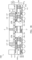
- Fig. 1A is a cross-sectional view of a semiconductor package structure 100a, which is not an embodiment according to the invention.
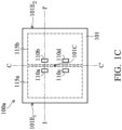
- Fig. 1C is a plan view of an arrangement of holes in a substrate 101 of the semiconductor package structure 100a shown in Fig. 1A
- Fig. 1A is a cross-sectional view of the semiconductor package structure 100a along line I-I' of Fig. 1C .
- the semiconductor package structure 100a may include a wafer-level semiconductor package, such as a flip-chip semiconductor package.
- the semiconductor package structure 100a may be mounted on a base (not shown).
- the semiconductor package structure 100a may be a system-on-chip (SOC) package structure.
- the base may include a printed circuit board (PCB) and may be formed of polypropylene (PP).
- the base may include a package substrate.
- the semiconductor package structure 100a is mounted on the base by a bonding process.
- the semiconductor package structure 100a may include bump structures 111.
- the bump structures 111 may be conductive ball structures (such as ball grid array (BGA)), conductive pillar structures, or conductive paste structures that are mounted on and electrically coupled to the base in the bonding process.
- BGA ball grid array
- the semiconductor package structure 100a includes a substrate 101.
- the substrate 101 has a wiring structure therein.
- the wiring structure in the substrate 101 is a fan-out structure, and may include one or more conductive pads 103, conductive vias 105, conductive layers 107 and conductive pillars 109.
- the wiring structure in the substrate 101 may be disposed in one or more inter-metal dielectric (IMD) layers.
- the IMD layers may be formed of organic materials, which include a polymer base material, non-organic materials, which include silicon nitride (SiNx), silicon oxide (SiOx), grapheme, or the like.
- the IMD layers are made of a polymer base material. It should be noted that the number and configuration of the IMD layers, the conductive pads 103, the conductive vias 105, the conductive layers 107 and the conductive pillars 109 shown in the figures and only some examples and are not limitations to the present invention.
- the semiconductor package structure 100a also includes a first semiconductor die 115a and a second semiconductor die 115b bonded onto the substrate 101 through a plurality of conductive structures 119.
- the substrate 101 has a first surface 101a and a second surface 101b opposite thereto, the first surface 101a is facing the first semiconductor die 115a and the second semiconductor die 115b, and the second surface 101b is facing the above-mentioned base.
- the conductive structures 119 are disposed over the first surface 101a and below the first semiconductor die 115a and the second semiconductor die 115b, and the bump structures 111 are disposed over the second surface 101b of the substrate 101.
- the first semiconductor die 115a and the second semiconductor die 115b are electrically coupled to the bump structures 111 through the conductive structures 119 and the wiring structure in the substrate 101.
- the conductive structures 119 may be controlled collapse chip connection (C4) structures. It should be noted that the number of semiconductor dies integrated in the semiconductor package structure 100a is not limited to that disclosed in the embodiment.
- the first semiconductor die 115a and the second semiconductor die 115b are active devices.
- the first semiconductor die 115a and the second semiconductor die 115b may be logic dies including a central processing unit (CPU), a graphics processing unit (GPU), a dynamic random access memory (DRAM) controller or any combination thereof.
- one or more passive devices are also bonded onto the substrate 101.
- the first semiconductor die 115a and the second semiconductor dies 115b are arranged side-by-side. In some embodiments, the first semiconductor die 115a and the second semiconductor dies 115b are separated by a molding material 117.
- the molding material 117 surrounds the first semiconductor die 115a and the second semiconductor die 115b, and adjoins the sidewalls of the first semiconductor die 115a and the second semiconductor die 115b.
- the molding material 117 includes a nonconductive material such as an epoxy, a resin, a moldable polymer, or another suitable molding material. In some embodiments, the molding material 117 is applied as a substantial liquid, and then is cured through a chemical reaction.
- the molding material 117 is an ultraviolet (UV) or thermally cured polymer applied as a gel or malleable solid, and then is cured through a UV or thermal curing process.
- the molding material 117 may be cured with a mold (not shown).
- the surfaces of the first semiconductor die 115a and the second semiconductor dies 115b facing away from the first surface 101a of the substrate 101 are exposed by the molding material 117, such that a heat dissipating device (not shown) can directly attached to the surfaces of the first semiconductor die 115a and the second semiconductor dies 115b.
- a heat dissipating device (not shown) can directly attached to the surfaces of the first semiconductor die 115a and the second semiconductor dies 115b.
- the semiconductor package structure 100a also includes a polymer material 121 disposed under the molding material 117, the first semiconductor die 115a and the second semiconductor die 115b, and between the conductive structures 119.
- the semiconductor package structure 100a further includes an underfill layer 123 interposed between the first surface 101a of the substrate 101 and the polymer material 121.
- the first semiconductor die 115a, the second semiconductor dies 115b and the molding material 117 are surrounded by the underfill layer 123.
- the polymer material 121 and the underfill layer 123 are disposed to compensate for differing coefficients of thermal expansion (CTEs) between the substrate 101, the conductive structures 119, the first semiconductor die 115a and the second semiconductor dies 115b.
- CTEs coefficients of thermal expansion
- the semiconductor package structure 100a includes a frame 113 attached to the first surface 101a of the substrate 101 through an adhesive layer 112.
- the first semiconductor die 115a and the second semiconductor die 115b are surrounded by the frame 113 and the adhesive layer 112.
- the frame 113 and the adhesive layer 112 are separated from the underfill layer 123 by a gap.
- the substrate 101 has a first edge 101E1 and a second edge 101E2 opposite thereto.
- the first edge 101 E1 and the second edge 101E2 are coplanar with sidewalls of the frame 113 and the adhesive layer 112.
- the substrate 101 of the semiconductor package structure 100a includes a first hole 110a and a second hole 110b formed on the second surface 101b.
- at least one of the first hole 110a and the second hole 110b penetrates through the substrate 101 from the first surface 101a to the second surface 101b.
- both the first hole 110a and the second hole 110b shown in Fig. 1A penetrate through the substrate 101, in some other embodiments, both the first hole 110a and the second hole 110b do not penetrate through the substrate 101 from the first surface 101a to the second surface 101b.
- the first hole 110a is covered by the first semiconductor die 115a
- the second hole 110b is covered by the second semiconductor die 115b.
- the first hole 110a is located within the projection of the first semiconductor die 115a on the substrate 101
- the second hole 110b is located within the projection of the second semiconductor die 115b on the substrate 101.
- the first semiconductor die 115a and the second semiconductor die 115b have a center line C-C' between them.
- the first hole 110a is disposed closer to the center line C-C' than the first edge 101E1 of the substrate 101
- the second hole 110b is disposed closer to the center line C-C' than the second edge 101E2 of the substrate 101.
- the first hole 110a and the second hole 110b are formed by a laser drilling process or another suitable process. It should be noted that the first hole 110a and the second hole 110b may be formed by the same forming process for the conductive pillars 109 in the wiring structure of the substrate 101. Moreover, the first semiconductor die 115a and the second semiconductor die 115b are bonded to the substrate 101 after forming the holes in the substrate 101. Therefore, the damage of the first semiconductor die 115a and the second semiconductor die 115b can be prevented.
- Fig. 1C is a plan view of an arrangement of holes in a substrate 101 of the semiconductor package structure 100a shown in Fig. 1A
- Fig. 1A is a cross-sectional view of the semiconductor package structure 100a along line I-I' of Fig. 1C
- Fig. 1C is the plan view from the bottom of the semiconductor package structure 100a.
- Fig. 1C is the plan view from the second surface 101b of the substrate 101, which the bump structures 111 are disposed on.
- the bump structures 111 are omitted for brevity.
- the substrate 101 includes more than two holes.
- the substrate 101 further includes a third hole 110c and the fourth hole 110d formed on the second surface 101b.
- the third hole 110c is covered by the first semiconductor die 115a
- the fourth hole 110d is covered by the second semiconductor die 115b.
- the substrate 101 has a center 101C, and the first hole 101a, the second hole 101b, the third hole 110c, and the fourth hole 110d are disposed closer to the center 101C than the first edge 101E1 and the second edge 101E2 of the substrate 101.
- the holes formed in the substrate 101 are designed to release the stress in the substrate 101, especially the stress concentrated in the region below the interface between two semiconductor dies (i.e. the first semiconductor die 115a and the second semiconductor die 115b). Since the semiconductor package structure 100a may be highly stressed due to the different coefficients of thermal expansion (CTEs) of the substrate 101 and the semiconductor dies, the holes formed in the substrate 101 can solve the warping or cracking problems caused by mismatched CTEs. As a result, the electrical connection within the semiconductor package structure 100a may not be damaged, and the reliability of the semiconductor package structure 100a may be increased.
- CTEs coefficients of thermal expansion
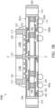
- Fig. 1B is a cross-sectional view of a semiconductor package structure 100b, which is not an embodiment according to the invention. Descriptions of elements of the embodiments hereinafter that are the same as or similar to those previously described with reference to Fig. 1A are omitted for brevity.
- the semiconductor package structure 100b includes a stress buffer layer 125 filled in the first hole 110a and the second hole 110b.
- the stress buffer layer 125 is made of a polymer material, such as a silicone resin or rubber.
- the stress buffer layer 125 is made of an organic resin, such as Ajinomoto Build-up Film (ABF).
- the stress buffer layer 125 may be formed by a spin coating process. In some other embodiments, a material of the stress buffer layer 125 may be dispensed in the first hole 110a and the second hole 110b, and an excess portion of the material of the stress buffer layer 125 may be removed. In some embodiments, the stress buffer layer 125 may be formed before bonding the first semiconductor die 115a and the second semiconductor die 115b to the substrate 101.
- the stress buffer layer 125 may fill the first hole 110a and the second hole 110b, and the surfaces of the stress buffer layer 125 are level with the second surface 101b of the substrate 101. In some other embodiments, the surfaces of the stress buffer layer 125 may not be level with the second surface 101b of the substrate 101 according to the actual manufacturing processes.
- Filling the first hole 110a and the second hole 110b with the stress buffer layer 125 may offer advantages like preventing the impurities and dusts from dropping into the first hole 110a and the second hole 110b during the handling process of the substrate 101.
- the warping or cracking problems caused by mismatched coefficients of thermal expansion in the semiconductor package structure 100b can be solved by the holes (including the first hole 110a and the second hole 110b) and the stress buffer layer 125 formed in the substrate 101. Accordingly, the electrical connection within the semiconductor package structure 100b may not be damaged, and the lifespan of the semiconductor package structure 100b may be increased.
- Fig. 2A is a plan view showing shapes of holes in a substrate 201A of a semiconductor package structure 200a, which is not an embodiment according to the invention
- Fig. 2B is a plan view showing shapes of holes in a substrate 201B of a semiconductor package structure 200b, which is not an embodiment according to the invention. Descriptions of elements of the embodiments hereinafter that are the same as or similar to those previously described with reference to Fig. 1C are omitted for brevity.
- the semiconductor package structure 200a has holes A, B, C, D, E, F, G, H, I, J, K and L in the substrate 201A, and the number of holes in the substrate 201A is much higher than that in the substrate 101 of the semiconductor package structure 100a.
- the holes A, B, C, D, E and F are covered by the first semiconductor die 115a
- the holes G, H, I, J, K and L are covered by the second semiconductor die 115b.
- the holes A-F are located within the projection of the first semiconductor die 115a on the substrate 201A
- the holes G-L are located within the projection of the second semiconductor die 115b on the substrate 201A.
- the holes A, B and C are arranged in a first array
- the holes D, E and F are arranged in a second array
- the holes G, H and I are arranged in a third array
- the holes J, K and L are arranged in a fourth array.
- the first array, the second array, the third array and the fourth array are parallel to the center line C-C' of the first semiconductor die 115a and the second semiconductor die 115b.
- the substrate 201B in the semiconductor package structure 200b has holes a, b, c, d, e, f, g, h, i, j, k and l, which are arranged in the same way as the holes A-L of the substrate 201A in the semiconductor package structure 200a.
- the difference between the substrate 201A and the substrate 201B is that the holes a-l have circular shapes in the plan view.
- the problems of stress concentrated at the corners of the holes A-L can be prevented in the substrate 201B due to the round shapes of the holes a-l. Therefore, there is a lower probability of the cracking problem occurring in the substrate 201B of the semiconductor package structure 200b.
- stress buffer layers may optionally be formed in the holes A-L of the semiconductor package structure 200a and in the holes a-l of the semiconductor package structure 200b. It should be noted that the holes A-L are symmetrically located about the center line C-C' in the plan view of Fig. 2A , and the holes a-l are symmetrically located about the center line C-C' in the plan view of Fig. 2B . In some other embodiments, the holes A-L are symmetrically located about the center 201C of the substrate 201A in the plan view of Fig. 2A , and the holes a-l are symmetrically located about the center 201C' of the substrate 201B in the plan view of Fig. 2B .
- Fig. 3A is a plan view showing arrangements of holes in a substrate 301A of a semiconductor package structure 300a, which is not an embodiment according to the invention
- Fig. 3B is a plan view showing arrangements of holes in a substrate 301B of a semiconductor package structure 300b, which is not an embodiment according to the invention. Descriptions of elements of the embodiments hereinafter that are the same as or similar to those previously described with reference to Fig. 2A are omitted for brevity.
- the semiconductor package structure 300a has holes A, B, C, D, E, and F in the substrate 301A.
- the holes A, B and C are covered by the first semiconductor die 115a, and the holes D, E and F are covered by the second semiconductor die 115b.
- the holes A-C are located within the projection of the first semiconductor die 115a on the substrate 301A, and the holes D-F are located within the projection of the second semiconductor die 115b on the substrate 301A.
- the holes A-F are arranged radially around the center 301C of the substrate 301A. In some other embodiments, the holes A-F are arranged radially around a center, and the center is located between the first semiconductor die 115a and the second semiconductor die 115b.
- the stress in the substrate 301A of the semiconductor package structure 300a can be released more efficiently.
- the number of the holes in the substrate 301A of the semiconductor package structure 300a can be less than the number of the holes in the substrate 201A of the semiconductor package structure 200a.
- the substrate 201A of the semiconductor package structure 200a which has holes A-L arranged parallel to the center line C-C', is more easily to be manufactured than the substrate 301A of the semiconductor package structure 300a, which has holes A-F arranged radially.
- the substrate 301B in the semiconductor package structure 300b has holes a, b, c, d, e, f, g, h, i, j, k, l, m and n arranged in a staggered arrangement in the substrate 301B.
- the holes a-g are covered by the first semiconductor die 115a and staggered in the direction of the center line C-C'
- the holes h-n are covered by the second semiconductor die 115b and staggered in the direction of the center line C-C'.
- the substrate 301B of the semiconductor package structure 300b can combine the above-mentioned benefits of the hole arrangements of the substrate 201A in the semiconductor package structure 200a and the substrate 301A of the semiconductor package structure 300a. Specifically, the holes a-n in the substrate 301B can be manufactured easily, and the stress in the substrate 301B can be released efficiently.
- stress buffer layers may optionally be formed in the holes A-F of the semiconductor package structure 300a and the holes a-n of the semiconductor package structure 300b.
- the holes A-F are symmetrically located about the center line C-C' in the plan view of Fig. 3A
- the holes a-n are symmetrically located about the center line C-C' in the plan view of Fig. 3B .
- the holes A-F are symmetrically located about the center 301C of the substrate 301A in the plan view of Fig. 3A
- the holes a-n are symmetrically located about the center 301C' of the substrate 301B in the plan view of Fig. 3B .
- Fig. 4A is a plan view showing locations of holes in a substrate 401A of a semiconductor package structure 400a, which is not an embodiment according to the invention
- Fig. 4B is a plan view showing locations of holes in a substrate 401B of a semiconductor package structure 400b, which is not an embodiment according to the invention. Descriptions of elements of the embodiments hereinafter that are the same as or similar to those previously described with reference to Fig. 2A are omitted for brevity.
- the substrate 401A in the semiconductor package structure 400a has holes A, B, C, D, E, F, G, H, I, J, K and L arranged in the same way as the holes A-L of the substrate 201A in the semiconductor package structure 200a shown in Fig. 2A .
- the holes A-L are arranged parallel to the center line C-C' in the substrate 401A.
- the difference between Figs. 2A and 4A is that the holes A-L in the substrate 401A are located closer to the center 401C of the substrate 401A than the holes A-L in the substrate 201A.
- the stress in the substrate 401A of the semiconductor package structure 400a which has holes A-L located closer to the center 401C of the substrate 401A, can be released more efficiently than the semiconductor package structure 200a.
- the substrate 401B in the semiconductor package structure 400b has holes a, b, c, d, e, f, g, h, i and j located along the peripheral edge of the substrate 401B.
- the holes a-j are located far from the center 401C' of the substrate 401B to reserve space in the middle of the substrate 401B for routing.
- the semiconductor substrate 400b of Fig. 4B can provide a better routing capability for the substrate 401B than the semiconductor substrate 400a of Fig. 4A .
- stress buffer layers may optionally be formed in the holes A-L of the semiconductor package structure 400a and the holes a-j of the semiconductor package structure 400b.
- the holes A-L are symmetrically located about the center line C-C' in the plan view of Fig. 4A
- the holes a-j are symmetrically located about the center line C-C' in the plan view of Fig. 4B .
- the holes A-L are symmetrically located about the center 401C of the substrate 401A in the plan view of Fig. 4A
- the holes a-j are symmetrically located about the center 401C' of the substrate 401B in the plan view of Fig. 4B .
- the holes formed in the substrate are designed to release the stress in the substrate, especially the stress concentrated in the region below the interface between two semiconductor dies. Since the semiconductor package structure may be highly stressed due to the different coefficients of thermal expansion (CTEs) of the substrate and the semiconductor dies, the holes formed in the substrate can solve the warping or cracking problems caused by mismatched CTEs. As a result, the electrical connection within the semiconductor package structure may remain undamaged, and the reliability and the lifespan of the semiconductor package structure may be increased.
- CTEs coefficients of thermal expansion
- Fig. 5A is a cross-sectional view of a semiconductor package structure 500a, which is not an embodiment according to the invention but useful for the understanding thereof. It should be noted that the semiconductor package structure 500a may include the same or similar components as that of the semiconductor package structures 100a and 100b, and for the sake of simplicity, those components will not be discussed in detail again.
- the following embodiment provides a substrate 502 including a first substrate 502a and a second substrate 502b. By using a plurality of small substrates instead of a large substrate, the reliability of the semiconductor package structure can be further improved according to some embodiments of the present disclosure.
- the first substrate 502a and the second substrate 502b are arranged side-by-side.
- the first substrate 502a has a first wiring structure therein
- the second substrate 502b has a second wiring structure therein.
- Each of the first substrate 502a and the second substrate 502b may be the same as or similar to the substrate 101 of the semiconductor package structures 100a and 100b.
- the first substrate 502a and the second substrate 502b may be homogenous or heterogeneous. That is, the first substrate 502a and the second substrate 502b may be the same as, similar to, or different from each other.
- Each of the first wiring structure in the first substrate 502a and the second wiring structure in the second substrate 502b may be the same as or similar to the wiring structure in the substrate 101.
- the first wiring structure in the first substrate 502a may be the same as or different from the second wiring structure in the second substrate 502b.
- each of the first wiring structure in the first substrate 502a and the second wiring structure in the second substrate 502b includes one or more conductive pads 103, conductive vias 105, conductive layers 107, and conductive pillars 109.
- the number of the conductive pads 103, the conductive vias 105, the conductive layers 107, and the conductive pillars 109 may be more or less in the first substrate 502a and the second substrate 502b than in the substrate 101.
- the substrate 502 may be viewed as partitioned into the first substrate 502a and the second substrate 502b. Therefore, the first substrate 502a and the second substrate 502b may be also referred to as the first substrate partition 502a and the second substrate partition 502b.
- the first substrate 502a and the second substrate 502b may be also referred to as the first substrate partition 502a and the second substrate partition 502b.
- a greater number of semiconductor dies are bonded onto a larger substrate.
- some related issues also occur. For example, as the volume of the substrate increases, more defects may be introduced during fabricating.
- the substrate 502 includes two or more substrate partitions, smaller substrate partitions can also be used. Accordingly, the reliability and the design flexibility of the semiconductor package structure can be improved.
- the substrate 502 further includes a molding material 504 surrounding the first substrate 502a and the second substrate 502b.
- the molding material 504 adjoins the sidewalls of the first substrate 502a and the second substrate 502b.
- the molding material 504 may be same as or similar to the molding material 117 of the semiconductor package structures 100a and 100b.
- the formation and the material of the molding material 504 may include the formation and the material as described above with respect to the molding material 117, and will not be repeated again.
- the first substrate 502a and the second substrate 502b are separated by the molding material 504.
- the semiconductor package structure 500a also includes a first semiconductor die 115a and a second semiconductor die 115b bonded onto the substrate 502 through a plurality of conductive structures 119.
- the first semiconductor die 115a is disposed over the first substrate 502a and electrically coupled to the first wiring structure in the first substrate 502a
- the second semiconductor die 115b is disposed over the second substrate 502b and electrically coupled to the second wiring structure in the second substrate 502b.
- the conductive structures 119 are disposed between the substrate 502 and the first semiconductor die 115a and between the substrate 502 and the second semiconductor die 115b, and the bump structures 111 are disposed below the substrate 502.
- the first semiconductor die 115a is electrically coupled to the bump structures 111 through the conductive structures 119 and the first wiring structure in the first substrate 502a
- the second semiconductor die 115b is electrically coupled to the bump structures 111 through the conductive structures 119 and the second wiring structure in the second substrate 502b.
- the thickness of the first substrate 502a and the thickness of the second substrate 502b are substantially the same in Figures, the present disclosure is not limit thereto. According to the claimed invention, the thickness of the first substrate 502a and the thickness of the second substrate 502b are different. For example, the thicknesses of the first substrate 502a and the second substrate 502b may depend on the characteristics of the semiconductor dies form thereon. According to the claimed invention, the semiconductor package structure 500a having substrates 502 with different thicknesses is used for dual-band antenna applications.
- the size of components adjacent to the first substrate 502a and/or the second substrate 502b may be adjusted to provide a planar surface.
- the conductive structures 119 disposed between the second semiconductor die 115b and the second substrate 502b may be thicker than the conductive structures 119 disposed between the first semiconductor die 115a and the first substrate 502a to provide a planar surface for bonding the semiconductor dies 115a, 115b thereon.
- the first semiconductor die 115a and the second semiconductor die 115b are surrounded by the molding material 117.
- the first semiconductor die 115a and the second semiconductor die 115b may be separated by the molding material 117.
- surfaces of the first semiconductor die 115a and the second semiconductor die 115b facing away from the substrate 502 are exposed by the molding material 117.
- the semiconductor package structure 500a includes a frame 113 disposed over the first substrate 502a and the second substrate 502b.
- the frame 113 may be attached to the substrate 502 through an adhesive layer 112.
- the first semiconductor die 115a and the second semiconductor die 115b may be surrounded by the frame 113.
- the frame 113 is separated from the underfill layer 123 by a gap.
- the sidewalls of the frame 113 may be coplanar with the sidewalls of the molding material 504.
- the frame 113 may include a metal ring or the inside of the frame 113 may include fluid. In some embodiments where the frame 113 including a metal ring, structural strength of the semiconductor package structure can be enforced. In some embodiments where the inside of the frame 113 including fluid, heat dissipation can be improved.
- the frame 113 is optional. In other embodiments, the semiconductor package structure does not include the frame 113.
- Fig. 5B is a cross-sectional view of a semiconductor package structure 500b, which is not an embodiment according to the invention but useful for the understanding thereof. Descriptions of elements of the embodiments hereinafter that are the same as or similar to those previously described with reference to Fig. 5A are omitted for brevity.
- the frame 113 is disposed on sidewalls of the substrate 502 and surrounds the first substrate 502a and the second substrate 502b.
- the frame 113 may be surrounded by the molding material 504.
- the frame 113 is separated from the first substrate 502a and the second substrate 502b by the molding material 504.
- the top surface of the frame 113 may be coplanar with the top surface of the molding material 504, and the bottom surface of the frame 113 may be coplanar with the bottom surface of the molding material 504.
- One of the methods to solve the warping or cracking problems caused by mismatched CTEs is to increase the thickness of the core layer of the substrate 502.
- this method may cause some problems, such as increased costs and complicated processing.
- the embodiment of the present disclosure providing the frame 113 disposed on sidewalls of the substrate 502 and surrounding the first substrate 502a and the second substrate 502b can increase the strength of the substrate 502, thereby reducing the thickness of the core layer of the substrate 502 and preventing the related issues.
- Figs. 6A-6C are plan views of semiconductor package structures 600a, 600b and 600c, which are not embodiments according to the invention but useful for the understanding thereof. For brevity, some components are omitted.
- Fig. 6A may be the plan view from the top of the semiconductor package structure 500a in Fig. 5A or the top of the semiconductor package structure 500b in Fig. 5B .
- the semiconductor package structure 600a includes the first substrate 502a, the second substrate 502b, the first semiconductor die 115a over the first substrate 502a, and the second semiconductor die 115b over the second substrate 502b.
- the arrangement is merely example and is not intended to be limiting.
- the first semiconductor die 115a may be disposed over the first substrate 502a and the second substrate 502b in some embodiments.
- the first semiconductor die 115a and the second semiconductor die 115b may be electrically connected with each other through wires 602 from the top surfaces of the first semiconductor die 115a and the second semiconductor die 115b. Further, in some embodiments, a portion of the molding material 504 is overlapped with a portion of the molding material 117 from the plan view.
- the semiconductor package structure 600b includes more than two substrates. As shown in Fig. 6B , the semiconductor package structure 600b further includes a third substrate 502c. The first substrate 502a, the second substrate 502b, and the third substrate 502c may be surrounded by the molding material 504. In some embodiments, the first substrate 502a, the second substrate 502b and the third substrate 502c are separated by the molding material 504.
- the third substrate 502c may have a third wiring structure.
- the third wiring structure in the third substrate 502c may be the same as or different from the first wiring structure in the first substrate 502a or the second wiring structure in the second substrate 502b.
- the first semiconductor die 115a and/or the second semiconductor die 115b is also electrically coupled to the third wiring structure in the third substrate 502c.
- the first semiconductor die 115a and the second semiconductor die 115b may be electrically connected with each other through the wires 602 from the top surfaces of the first semiconductor die 115a and the second semiconductor die 115b.
- the second semiconductor die 115b is disposed over the second substrate 502b and the third substrate 502c, wherein the third substrate 502c is disposed adjacent to the first substrate 502a and the second substrate 502b.
- the arrangement is merely example and is not intended to be limiting.
- the third substrate 502c may be disposed adjacent to the first substrate 502a or the second substrate 502b only.
- the first semiconductor die 115a may be disposed over the first substrate 502a and the third substrate 502c.
- the semiconductor package structure 600c includes more than two semiconductor dies. As shown in Fig. 6C , the semiconductor package structure 600c further includes a third semiconductor die 115c disposed over the second substrate 502b and electrically coupled to the second wiring structure in the second substrate 502b. The third semiconductor die 115c may be bonded onto the second substrate 502b through a plurality of conductive structures (not shown).
- the first semiconductor die 115a, the second semiconductor die 115b and the third semiconductor die 115c are surrounded by the molding material 117. In some embodiments, the first semiconductor die 115a, the second semiconductor die 115b and the third semiconductor die 115c are separated by the molding material 117. The third semiconductor die 115c may be the same as or different from the first semiconductor die 115a or the second semiconductor die 115b.
- the first semiconductor die 115a and the second semiconductor die 115b may be electrically connected with each other through the wires 602a from the top surfaces of the first semiconductor die 115a and the second semiconductor die 115b, and the first semiconductor die 115a and the third semiconductor die 115c may be electrically connected with each other through the wires 602b from the top surfaces of the first semiconductor die 115a and the third semiconductor die 115c.
- the arrangement is merely example and is not intended to be limiting.
- the second semiconductor die 115b and the third semiconductor die 115c may be electrically connected with each other through wires from the top surfaces of the second semiconductor die 115b and the third semiconductor die 115c.
- the third semiconductor die 115c is disposed over the second substrate 502b, and the third substrate 502c is disposed adjacent to the first semiconductor die 115a and the second semiconductor die 115b.
- the arrangement is merely example and is not intended to be limiting.
- the third substrate 502c may be disposed over the first substrate 502a or an additional substrate (not shown). It should be noted that the number of semiconductor dies and the number of substrates in the semiconductor package structures 600a-600c are not limited to that disclosed in the embodiment.
- Fig. 7 is a cross-sectional view of a semiconductor package structure 700, which is not an embodiment according to the invention but useful for the understanding thereof.
- the semiconductor package structure 700 may include the same or similar components as that of the semiconductor package structures 500a and 500b, and for the sake of simplicity, those components will not be discussed in detail again.
- a redistribution layer 702 is disposed over the substrate 502.
- the redistribution layer 702 includes one or more dielectric layers, wiring layers, or any other suitable structures.
- the redistribution layer 702 may cover the first substrate 502a and the second substrate 502b, and the redistribution layer 702 may be electrically coupled to the first wiring structure in the first substrate 502a and the second wiring structure in the second substrate 502b.
- the redistribution layer 702 may be bonded onto the substrate 502 through a plurality of conductive structures 119.
- the conductive structures 119 are disposed between the redistribution layer 702 and the first substrate 502a and between the redistribution layer 702 and the second substrate 502b.
- the redistribution layer 702 is electrically coupled to the bump structures 111 through the conductive structures 119, the first wiring structure in the first substrate 502a, and the second wiring structure in the second substrate 502b.
- the size of components adjacent to the first substrate 502a and/or the second substrate 502b may be adjusted to provide a planar surface.
- the first substrate 502a is thicker than the second substrate 502b, and the conductive structures 119 disposed between the redistribution layer 702 and the second substrate 502b may be thicker than the conductive structures 119 disposed between the redistribution layer 702 and the first substrate 502a to provide a planar surface for bonding the redistribution layer 702 thereon.
- the redistribution layer 702 covers the frame 113, and the frame 113 is thicker than the first substrate 502a and the second substrate 502b to support the redistribution layer 702.
- the sidewalls of the redistribution layer 702 may be coplanar with the sidewalls of the molding material 504.
- the redistribution layer 702 exposes the frame 113 or partially covers the frame 113.
- the frame 113 may surround the redistribution layer 702.
- a double-sided substrate fabricating process can be used for fabricating thin substrates.
- interconnect structures are simultaneously formed on opposite surfaces of a carrier substrate, and then the interconnect structures are separated from the carrier substrate to form the thin substrates.
- Fig. 8 is a plan view of a semiconductor package structure 800, in accordance with the embodiments of the invention.
- the semiconductor package structure 800 is an exemplary embodiment including dual-band antenna structures.
- the semiconductor package structure 800 may be used for 5G application.
- some components are omitted.
- the semiconductor package structure 800 includes a plurality of first antenna structures 804a and a plurality of second antenna structures 804b.
- the first antenna structures 804a are disposed over the first substrate 502a and electrically coupled to the first wiring structure in the first substrate 502a.
- the second antenna structures 804b are disposed over the second substrate 502b and electrically coupled to the second wiring structure in the second substrate 502b.
- the semiconductor package structure 800 further includes a connector 802 disposed over the second substrate 502b and not disposed over the first substrate 502a.
- the substrate of the semiconductor package structure includes substrate partitions with different thicknesses for different applications.
- the first antenna structures 804a and the second antenna structures 804b are used for different bands, and the thicknesses of the first substrate 502a and the second substrate 502b is different. Therefore, antenna structures with different bands are disposed in one semiconductor package structure 800.
- the reliability and the design flexibility of the semiconductor package structure 800 can be improved, and the cost of manufacture can be reduced, according to some embodiments.
- a semiconductor package structure having a plurality of substrates arranged side-by-side is provided.
- a plurality of small substrates it is unnecessary to form a large substrate for bonding a great number of semiconductor dies thereon. Since it is easier to form a small substrate than a large substrate, the reliability of the semiconductor package structure can be improved, according to the claimed invention.
- the substrates have different thicknesses for different applications.
- antenna structures for different bands are disposed in one semiconductor package structure. Therefore, the design flexibility of the semiconductor package structure can be improved.
- thickness of components adjacent to the substrates can be adjusted to provide a planar surface.
- the semiconductor package structure includes a frame surrounding the substrates to increase the strength of the semiconductor package structure. Therefore, the thickness of the substrates can be reduced without decreasing the strength of the substrates. Further, in some embodiments, depending on the material of the frame, structural strength of the semiconductor package structure can be enforced, or heat dissipation can be improved.
- the semiconductor package structures in accordance with some embodiments of the disclosure can be used to form a three-dimensional (3D) package, a 2.5D package, a fan-out package, or another suitable package.
- the arrangements, the shapes, and the locations of the holes in the substrate can be adjusted according to the types of the application.
Landscapes
- Structures Or Materials For Encapsulating Or Coating Semiconductor Devices Or Solid State Devices (AREA)
Claims (14)
- Halbleiterpackagestruktur (800), die aufweist:ein Substrat, aufweisend:ein erstes Substrat (502a) mit einer ersten Verdrahtungsstruktur; undein zweites Substrat (502b), das an das erste Substrat (502a) angrenzt und eine zweite Verdrahtungsstruktur aufweist,wobei das erste Substrat (502a) und das zweite Substrat (502b) von einer ersten Formmasse (504) umgeben sind;einen ersten Halbleiterdie (115a), der über dem Substrat angeordnet und elektrisch mit der ersten Verdrahtungsstruktur verbunden ist; undeinen zweiten Halbleiterdie (115b), der über dem Substrat angeordnet und elektrisch mit der zweiten Verdrahtungsstruktur verbunden ist,dadurch gekennzeichnet, dass die Halbleiterpackagestruktur ferner eine Vielzahl von ersten Antennenstrukturen (804a) aufweist, die über dem ersten Substrat (502a) angeordnet und elektrisch mit der ersten Verdrahtungsstruktur gekoppelt sind,und eine Vielzahl von zweiten Antennenstrukturen (804b), die über dem zweiten Substrat (502b) angeordnet und elektrisch mit der zweiten Verdrahtungsstruktur verbunden sind,wobei das erste Substrat (502a) und das zweite Substrat (502b) unterschiedliche Dicken aufweisen und die ersten Antennenstrukturen (804a) und die zweiten Antennenstrukturen (804b) zur Verwendung für unterschiedliche Bänder konfiguriert sind.
- Halbleiterpackagestruktur (800) nach Anspruch 1, wobei das erste Substrat (502a) und das zweite Substrat (502b) homogen oder heterogen ist.
- Halbleiterpackagestruktur (800) nach Anspruch 1 oder 2, wobei das erste Substrat (502a) und das zweite Substrat (502b) durch das erste Formmaterial getrennt sind und/oder der erste und der zweite Halbleiterdie (115a, 115b) von einem zweiten Formmaterial (117) umgeben und getrennt sind, wobei die vom Substrat abgewandten Oberflächen des ersten Halbleiterdies (115a) und des zweiten Halbleiterdies (115b) von dem zweiten Formmaterial freigelegt sein können.
- Halbleiterpackagestruktur (800) nach einem der vorhergehenden Ansprüche, die ferner ein drittes Substrat (502c) neben dem ersten Substrat (502a) und/oder dem zweiten Substrat (502b) aufweist, wobei das dritte Substrat eine dritte Verdrahtungsstruktur aufweist, wobei das erste Substrat, das zweite Substrat und das dritte Substrat von dem ersten Formmaterial umgeben sind.
- Halbleiterpackagestruktur (800) nach Anspruch 4, wobei das erste Substrat (502a), das zweite Substrat (502b) und das dritte Substrat (502c) durch das erste Formmaterial getrennt sind; und/oder wobei der erste Halbleiterdie (115a) oder der zweite Halbleiterdie (115b) mit der dritten Verdrahtungsstruktur auch elektrisch verbunden ist.
- Die Halbleiterpackagestruktur (800) nach einem der vorhergehenden Ansprüche, die ferner einen dritten Halbleiterdie (115c) aufweist, der über dem Substrat angeordnet und mit der ersten Verdrahtungsstruktur und/oder der zweiten Verdrahtungsstruktur elektrisch verbunden ist.
- Halbleiterpackagestruktur (800) nach Anspruch 6, wobei der erste Halbleiterdie (115a), der zweite Halbleiterdie (115b) und der dritte Halbleiterdie (115c) von einem zweiten Formmaterial umgeben und getrennt sind.
- Halbleiterpackagestruktur (800) nach einem der vorhergehenden Ansprüche, ferner aufweisend;eine Vielzahl von leitenden Strukturen (119), die zwischen dem Substrat und dem ersten Halbleiterdie (115a) und zwischen dem Substrat und dem zweiten Halbleiterdie (115b) angeordnet sind; undeine Vielzahl von Bump-Strukturen (111), die unter dem Substrat angeordnet sind, wobei der erste Halbleiterdie (115a) und der zweite Halbleiterdie (115b) über die Vielzahl von leitenden Strukturen (119), die erste Verdrahtungsstruktur bzw. die zweite Verdrahtungsstruktur mit der Vielzahl von Bump-Strukturen elektrisch verbunden sind.
- Die Halbleiterpackagestruktur (800) nach einem der vorhergehenden Ansprüche, die ferner einen Rahmen (113) aufweist, der über dem ersten Substrat (502a) und dem zweiten Substrat (502b) angeordnet ist, wobei der Rahmen den ersten Halbleiterdie (115a) und den zweiten Halbleiterdie (115b) umgibt; oder einen Rahmen, der das erste Substrat und das zweite Substrat umgibt, wobei der Rahmen von dem ersten Formmaterial umgeben ist.
- Die Halbleiterpackagestruktur (800) nach einem der vorhergehenden Ansprüche, die ferner Folgendes aufweist:eine Umverteilungsschicht (702), die über dem ersten Substrat (502a) und dem zweiten Substrat (502b) angeordnet ist, wobei die Umverteilungsschicht mit der ersten Verdrahtungsstruktur und der zweiten Verdrahtungsstruktur elektrisch gekoppelt ist; undeinen Rahmen (113), der das erste Substrat (502a) und das zweite Substrat (502b) umgibt.
- Halbleiterpackagestruktur (800) nach Anspruch 10, ferner eine Vielzahl von leitenden Strukturen (119) aufweist, die zwischen der Umverteilungsschicht (702) und dem ersten Substrat (502a) und zwischen der Umverteilungsschicht und dem zweiten Substrat (502b) angeordnet sind.
- Halbleiterpackagestruktur (800) nach Anspruch 11, wobei das erste Substrat (502a) dicker ist als das zweite Substrat (502b), und die Vielzahl von leitenden Strukturen (119), die zwischen der Umverteilungsschicht (702) und dem zweiten Substrat angeordnet sind, dicker ist als die Vielzahl von leitenden Strukturen, die zwischen der Umverteilungsschicht und dem ersten Substrat angeordnet sind.
- Halbleiterpackungsstruktur (800) nach einem der Ansprüche 10 bis 12, wobei die Umverteilungsschicht (702) den Rahmen (113) bedeckt; oder wobei die Umverteilungsschicht das erste Substrat (502a) und das zweite Substrat (502b) bedeckt und den Rahmen freilegt.
- Die Halbleiterpackagestruktur (800) nach einem der vorhergehenden Ansprüche, die ferner einen Verbinder (802) aufweist, der über dem zweiten Substrat (502b) und nicht über dem ersten Substrat (502a) angeordnet ist.
Priority Applications (1)
| Application Number | Priority Date | Filing Date | Title |
|---|---|---|---|
| EP24168496.8A EP4376067A3 (de) | 2019-03-14 | 2020-03-12 | Halbleitergehäusestruktur |
Applications Claiming Priority (2)
| Application Number | Priority Date | Filing Date | Title |
|---|---|---|---|
| US201962818174P | 2019-03-14 | 2019-03-14 | |
| US16/813,898 US11387176B2 (en) | 2017-03-14 | 2020-03-10 | Semiconductor package structure |
Related Child Applications (2)
| Application Number | Title | Priority Date | Filing Date |
|---|---|---|---|
| EP24168496.8A Division EP4376067A3 (de) | 2019-03-14 | 2020-03-12 | Halbleitergehäusestruktur |
| EP24168496.8A Division-Into EP4376067A3 (de) | 2019-03-14 | 2020-03-12 | Halbleitergehäusestruktur |
Publications (2)
| Publication Number | Publication Date |
|---|---|
| EP3709344A1 EP3709344A1 (de) | 2020-09-16 |
| EP3709344B1 true EP3709344B1 (de) | 2024-05-08 |
Family
ID=69804748
Family Applications (2)
| Application Number | Title | Priority Date | Filing Date |
|---|---|---|---|
| EP20162559.7A Active EP3709344B1 (de) | 2019-03-14 | 2020-03-12 | Halbleitergehäusestruktur |
| EP24168496.8A Pending EP4376067A3 (de) | 2019-03-14 | 2020-03-12 | Halbleitergehäusestruktur |
Family Applications After (1)
| Application Number | Title | Priority Date | Filing Date |
|---|---|---|---|
| EP24168496.8A Pending EP4376067A3 (de) | 2019-03-14 | 2020-03-12 | Halbleitergehäusestruktur |
Country Status (3)
| Country | Link |
|---|---|
| EP (2) | EP3709344B1 (de) |
| CN (2) | CN118448360A (de) |
| TW (1) | TWI721820B (de) |
Families Citing this family (11)
| Publication number | Priority date | Publication date | Assignee | Title |
|---|---|---|---|---|
| US11362044B2 (en) | 2017-03-14 | 2022-06-14 | Mediatek Inc. | Semiconductor package structure |
| US11387176B2 (en) | 2017-03-14 | 2022-07-12 | Mediatek Inc. | Semiconductor package structure |
| US12424531B2 (en) | 2017-03-14 | 2025-09-23 | Mediatek Inc. | Semiconductor package structure |
| US11171113B2 (en) | 2017-03-14 | 2021-11-09 | Mediatek Inc. | Semiconductor package structure having an annular frame with truncated corners |
| US11264337B2 (en) | 2017-03-14 | 2022-03-01 | Mediatek Inc. | Semiconductor package structure |
| US10784211B2 (en) | 2017-03-14 | 2020-09-22 | Mediatek Inc. | Semiconductor package structure |
| CN112103277B (zh) * | 2019-06-17 | 2023-09-01 | 联发科技股份有限公司 | 半导体封装结构 |
| CN112908972A (zh) * | 2021-01-08 | 2021-06-04 | 日月光半导体制造股份有限公司 | 封装结构及其形成方法 |
| US20220277127A1 (en) * | 2021-02-26 | 2022-09-01 | Taiwan Semiconductor Manufacturing Company, Ltd. | Bonded Semiconductor Device And Method For Forming The Same |
| US11973058B2 (en) * | 2021-11-25 | 2024-04-30 | International Business Machines Corporation | Multiple die assembly |
| US20250022810A1 (en) * | 2023-07-10 | 2025-01-16 | Taiwan Semiconductor Manufacturing Company Limited | Semiconductor package substrate with stress buffer pads and methods for making the same |
Family Cites Families (15)
| Publication number | Priority date | Publication date | Assignee | Title |
|---|---|---|---|---|
| CN1543298A (zh) * | 2000-06-27 | 2004-11-03 | ���µ�����ҵ��ʽ���� | 陶瓷叠层器件 |
| JP2008545274A (ja) * | 2005-06-30 | 2008-12-11 | フェアチャイルド セミコンダクター コーポレイション | 半導体ダイ・パッケージ及びその製造方法 |
| KR20090097425A (ko) * | 2008-03-11 | 2009-09-16 | 주식회사 하이닉스반도체 | 반도체 소자의 게이트 절연막 형성 방법 |
| US8313984B2 (en) * | 2008-03-19 | 2012-11-20 | Ati Technologies Ulc | Die substrate with reinforcement structure |
| WO2013119309A1 (en) * | 2012-02-08 | 2013-08-15 | Xilinx, Inc. | Stacked die assembly with multiple interposers |
| JP2013187740A (ja) * | 2012-03-08 | 2013-09-19 | Renesas Electronics Corp | 半導体装置 |
| US9312193B2 (en) * | 2012-11-09 | 2016-04-12 | Taiwan Semiconductor Manufacturing Company, Ltd. | Stress relief structures in package assemblies |
| CN203192781U (zh) * | 2012-12-13 | 2013-09-11 | 日月光半导体(上海)有限公司 | 封装基板条构造 |
| US9412662B2 (en) * | 2014-01-28 | 2016-08-09 | Taiwan Semiconductor Manufacturing Company, Ltd. | Structure and approach to prevent thin wafer crack |
| KR101676916B1 (ko) * | 2014-08-20 | 2016-11-16 | 앰코 테크놀로지 코리아 주식회사 | 반도체 디바이스의 제조 방법 및 이에 따른 반도체 디바이스 |
| CN104409366A (zh) * | 2014-11-19 | 2015-03-11 | 三星半导体(中国)研究开发有限公司 | 芯片封装方法及封装基底 |
| US10546835B2 (en) * | 2015-12-22 | 2020-01-28 | Intel Corporation | Microelectronic devices designed with efficient partitioning of high frequency communication devices integrated on a package fabric |
| KR102666151B1 (ko) * | 2016-12-16 | 2024-05-17 | 삼성전자주식회사 | 반도체 패키지 |
| US10784211B2 (en) * | 2017-03-14 | 2020-09-22 | Mediatek Inc. | Semiconductor package structure |
| US10867925B2 (en) * | 2018-07-19 | 2020-12-15 | Taiwan Semiconductor Manufacturing Co., Ltd. | Method for forming chip package structure |
-
2020
- 2020-03-12 CN CN202410369045.XA patent/CN118448360A/zh active Pending
- 2020-03-12 EP EP20162559.7A patent/EP3709344B1/de active Active
- 2020-03-12 TW TW109108155A patent/TWI721820B/zh active
- 2020-03-12 CN CN202010169324.3A patent/CN111696979B/zh active Active
- 2020-03-12 EP EP24168496.8A patent/EP4376067A3/de active Pending
Also Published As
| Publication number | Publication date |
|---|---|
| CN111696979B (zh) | 2024-04-23 |
| EP3709344A1 (de) | 2020-09-16 |
| EP4376067A2 (de) | 2024-05-29 |
| TWI721820B (zh) | 2021-03-11 |
| CN111696979A (zh) | 2020-09-22 |
| TW202034470A (zh) | 2020-09-16 |
| CN118448360A (zh) | 2024-08-06 |
| EP4376067A3 (de) | 2024-09-04 |
Similar Documents
| Publication | Publication Date | Title |
|---|---|---|
| EP3709344B1 (de) | Halbleitergehäusestruktur | |
| US11948895B2 (en) | Semiconductor package structure | |
| EP3754698B1 (de) | Halbleitergehäusestruktur | |
| US11942439B2 (en) | Semiconductor package structure | |
| US11862578B2 (en) | Semiconductor package structure | |
| US10515887B2 (en) | Fan-out package structure having stacked carrier substrates and method for forming the same | |
| US12002742B2 (en) | Semiconductor package structure | |
| US12142598B2 (en) | Semiconductor package structure having an annular frame with truncated corners | |
| EP3671831B1 (de) | Halbleiterpaketstruktur | |
| US12424531B2 (en) | Semiconductor package structure | |
| EP3624181B1 (de) | Halbleitergehäusestruktur mit einem rahmen mit abgeschnittenen ecken |
Legal Events
| Date | Code | Title | Description |
|---|---|---|---|
| PUAI | Public reference made under article 153(3) epc to a published international application that has entered the european phase |
Free format text: ORIGINAL CODE: 0009012 |
|
| STAA | Information on the status of an ep patent application or granted ep patent |
Free format text: STATUS: THE APPLICATION HAS BEEN PUBLISHED |
|
| AK | Designated contracting states |
Kind code of ref document: A1 Designated state(s): AL AT BE BG CH CY CZ DE DK EE ES FI FR GB GR HR HU IE IS IT LI LT LU LV MC MK MT NL NO PL PT RO RS SE SI SK SM TR |
|
| AX | Request for extension of the european patent |
Extension state: BA ME |
|
| STAA | Information on the status of an ep patent application or granted ep patent |
Free format text: STATUS: REQUEST FOR EXAMINATION WAS MADE |
|
| 17P | Request for examination filed |
Effective date: 20210312 |
|
| RBV | Designated contracting states (corrected) |
Designated state(s): AL AT BE BG CH CY CZ DE DK EE ES FI FR GB GR HR HU IE IS IT LI LT LU LV MC MK MT NL NO PL PT RO RS SE SI SK SM TR |
|
| P01 | Opt-out of the competence of the unified patent court (upc) registered |
Effective date: 20230607 |
|
| GRAP | Despatch of communication of intention to grant a patent |
Free format text: ORIGINAL CODE: EPIDOSNIGR1 |
|
| STAA | Information on the status of an ep patent application or granted ep patent |
Free format text: STATUS: GRANT OF PATENT IS INTENDED |
|
| RIC1 | Information provided on ipc code assigned before grant |
Ipc: H01L 23/00 20060101ALI20231104BHEP Ipc: H01L 23/538 20060101ALI20231104BHEP Ipc: H01L 23/498 20060101ALI20231104BHEP Ipc: H01L 23/36 20060101ALI20231104BHEP Ipc: H01L 23/66 20060101ALI20231104BHEP Ipc: H01L 25/065 20060101ALI20231104BHEP Ipc: H01L 23/31 20060101AFI20231104BHEP |
|
| INTG | Intention to grant announced |
Effective date: 20231127 |
|
| GRAS | Grant fee paid |
Free format text: ORIGINAL CODE: EPIDOSNIGR3 |
|
| GRAA | (expected) grant |
Free format text: ORIGINAL CODE: 0009210 |
|
| STAA | Information on the status of an ep patent application or granted ep patent |
Free format text: STATUS: THE PATENT HAS BEEN GRANTED |
|
| AK | Designated contracting states |
Kind code of ref document: B1 Designated state(s): AL AT BE BG CH CY CZ DE DK EE ES FI FR GB GR HR HU IE IS IT LI LT LU LV MC MK MT NL NO PL PT RO RS SE SI SK SM TR |
|
| REG | Reference to a national code |
Ref country code: GB Ref legal event code: FG4D |
|
| REG | Reference to a national code |
Ref country code: CH Ref legal event code: EP |
|
| REG | Reference to a national code |
Ref country code: DE Ref legal event code: R096 Ref document number: 602020030481 Country of ref document: DE |
|
| REG | Reference to a national code |
Ref country code: IE Ref legal event code: FG4D |
|
| REG | Reference to a national code |
Ref country code: LT Ref legal event code: MG9D |
|
| REG | Reference to a national code |
Ref country code: NL Ref legal event code: MP Effective date: 20240508 |
|
| PG25 | Lapsed in a contracting state [announced via postgrant information from national office to epo] |
Ref country code: IS Free format text: LAPSE BECAUSE OF FAILURE TO SUBMIT A TRANSLATION OF THE DESCRIPTION OR TO PAY THE FEE WITHIN THE PRESCRIBED TIME-LIMIT Effective date: 20240908 |
|
| PG25 | Lapsed in a contracting state [announced via postgrant information from national office to epo] |
Ref country code: BG Free format text: LAPSE BECAUSE OF FAILURE TO SUBMIT A TRANSLATION OF THE DESCRIPTION OR TO PAY THE FEE WITHIN THE PRESCRIBED TIME-LIMIT Effective date: 20240508 |
|
| PG25 | Lapsed in a contracting state [announced via postgrant information from national office to epo] |
Ref country code: FI Free format text: LAPSE BECAUSE OF FAILURE TO SUBMIT A TRANSLATION OF THE DESCRIPTION OR TO PAY THE FEE WITHIN THE PRESCRIBED TIME-LIMIT Effective date: 20240508 Ref country code: HR Free format text: LAPSE BECAUSE OF FAILURE TO SUBMIT A TRANSLATION OF THE DESCRIPTION OR TO PAY THE FEE WITHIN THE PRESCRIBED TIME-LIMIT Effective date: 20240508 |
|
| PG25 | Lapsed in a contracting state [announced via postgrant information from national office to epo] |
Ref country code: GR Free format text: LAPSE BECAUSE OF FAILURE TO SUBMIT A TRANSLATION OF THE DESCRIPTION OR TO PAY THE FEE WITHIN THE PRESCRIBED TIME-LIMIT Effective date: 20240809 |
|
| PG25 | Lapsed in a contracting state [announced via postgrant information from national office to epo] |
Ref country code: PT Free format text: LAPSE BECAUSE OF FAILURE TO SUBMIT A TRANSLATION OF THE DESCRIPTION OR TO PAY THE FEE WITHIN THE PRESCRIBED TIME-LIMIT Effective date: 20240909 |
|
| REG | Reference to a national code |
Ref country code: AT Ref legal event code: MK05 Ref document number: 1685741 Country of ref document: AT Kind code of ref document: T Effective date: 20240508 |
|
| PG25 | Lapsed in a contracting state [announced via postgrant information from national office to epo] |
Ref country code: NL Free format text: LAPSE BECAUSE OF FAILURE TO SUBMIT A TRANSLATION OF THE DESCRIPTION OR TO PAY THE FEE WITHIN THE PRESCRIBED TIME-LIMIT Effective date: 20240508 |
|
| PG25 | Lapsed in a contracting state [announced via postgrant information from national office to epo] |
Ref country code: ES Free format text: LAPSE BECAUSE OF FAILURE TO SUBMIT A TRANSLATION OF THE DESCRIPTION OR TO PAY THE FEE WITHIN THE PRESCRIBED TIME-LIMIT Effective date: 20240508 |
|
| PG25 | Lapsed in a contracting state [announced via postgrant information from national office to epo] |
Ref country code: AT Free format text: LAPSE BECAUSE OF FAILURE TO SUBMIT A TRANSLATION OF THE DESCRIPTION OR TO PAY THE FEE WITHIN THE PRESCRIBED TIME-LIMIT Effective date: 20240508 |
|
| PG25 | Lapsed in a contracting state [announced via postgrant information from national office to epo] |
Ref country code: PL Free format text: LAPSE BECAUSE OF FAILURE TO SUBMIT A TRANSLATION OF THE DESCRIPTION OR TO PAY THE FEE WITHIN THE PRESCRIBED TIME-LIMIT Effective date: 20240508 |
|
| PG25 | Lapsed in a contracting state [announced via postgrant information from national office to epo] |
Ref country code: LV Free format text: LAPSE BECAUSE OF FAILURE TO SUBMIT A TRANSLATION OF THE DESCRIPTION OR TO PAY THE FEE WITHIN THE PRESCRIBED TIME-LIMIT Effective date: 20240508 |
|
| PG25 | Lapsed in a contracting state [announced via postgrant information from national office to epo] |
Ref country code: PT Free format text: LAPSE BECAUSE OF FAILURE TO SUBMIT A TRANSLATION OF THE DESCRIPTION OR TO PAY THE FEE WITHIN THE PRESCRIBED TIME-LIMIT Effective date: 20240909 Ref country code: PL Free format text: LAPSE BECAUSE OF FAILURE TO SUBMIT A TRANSLATION OF THE DESCRIPTION OR TO PAY THE FEE WITHIN THE PRESCRIBED TIME-LIMIT Effective date: 20240508 Ref country code: NO Free format text: LAPSE BECAUSE OF FAILURE TO SUBMIT A TRANSLATION OF THE DESCRIPTION OR TO PAY THE FEE WITHIN THE PRESCRIBED TIME-LIMIT Effective date: 20240808 Ref country code: NL Free format text: LAPSE BECAUSE OF FAILURE TO SUBMIT A TRANSLATION OF THE DESCRIPTION OR TO PAY THE FEE WITHIN THE PRESCRIBED TIME-LIMIT Effective date: 20240508 Ref country code: LV Free format text: LAPSE BECAUSE OF FAILURE TO SUBMIT A TRANSLATION OF THE DESCRIPTION OR TO PAY THE FEE WITHIN THE PRESCRIBED TIME-LIMIT Effective date: 20240508 Ref country code: IS Free format text: LAPSE BECAUSE OF FAILURE TO SUBMIT A TRANSLATION OF THE DESCRIPTION OR TO PAY THE FEE WITHIN THE PRESCRIBED TIME-LIMIT Effective date: 20240908 Ref country code: HR Free format text: LAPSE BECAUSE OF FAILURE TO SUBMIT A TRANSLATION OF THE DESCRIPTION OR TO PAY THE FEE WITHIN THE PRESCRIBED TIME-LIMIT Effective date: 20240508 Ref country code: GR Free format text: LAPSE BECAUSE OF FAILURE TO SUBMIT A TRANSLATION OF THE DESCRIPTION OR TO PAY THE FEE WITHIN THE PRESCRIBED TIME-LIMIT Effective date: 20240809 Ref country code: FI Free format text: LAPSE BECAUSE OF FAILURE TO SUBMIT A TRANSLATION OF THE DESCRIPTION OR TO PAY THE FEE WITHIN THE PRESCRIBED TIME-LIMIT Effective date: 20240508 Ref country code: ES Free format text: LAPSE BECAUSE OF FAILURE TO SUBMIT A TRANSLATION OF THE DESCRIPTION OR TO PAY THE FEE WITHIN THE PRESCRIBED TIME-LIMIT Effective date: 20240508 Ref country code: BG Free format text: LAPSE BECAUSE OF FAILURE TO SUBMIT A TRANSLATION OF THE DESCRIPTION OR TO PAY THE FEE WITHIN THE PRESCRIBED TIME-LIMIT Effective date: 20240508 Ref country code: AT Free format text: LAPSE BECAUSE OF FAILURE TO SUBMIT A TRANSLATION OF THE DESCRIPTION OR TO PAY THE FEE WITHIN THE PRESCRIBED TIME-LIMIT Effective date: 20240508 Ref country code: RS Free format text: LAPSE BECAUSE OF FAILURE TO SUBMIT A TRANSLATION OF THE DESCRIPTION OR TO PAY THE FEE WITHIN THE PRESCRIBED TIME-LIMIT Effective date: 20240808 |
|
| PG25 | Lapsed in a contracting state [announced via postgrant information from national office to epo] |
Ref country code: DK Free format text: LAPSE BECAUSE OF FAILURE TO SUBMIT A TRANSLATION OF THE DESCRIPTION OR TO PAY THE FEE WITHIN THE PRESCRIBED TIME-LIMIT Effective date: 20240508 |
|
| PG25 | Lapsed in a contracting state [announced via postgrant information from national office to epo] |
Ref country code: EE Free format text: LAPSE BECAUSE OF FAILURE TO SUBMIT A TRANSLATION OF THE DESCRIPTION OR TO PAY THE FEE WITHIN THE PRESCRIBED TIME-LIMIT Effective date: 20240508 |
|
| PG25 | Lapsed in a contracting state [announced via postgrant information from national office to epo] |
Ref country code: CZ Free format text: LAPSE BECAUSE OF FAILURE TO SUBMIT A TRANSLATION OF THE DESCRIPTION OR TO PAY THE FEE WITHIN THE PRESCRIBED TIME-LIMIT Effective date: 20240508 |
|
| PG25 | Lapsed in a contracting state [announced via postgrant information from national office to epo] |
Ref country code: SK Free format text: LAPSE BECAUSE OF FAILURE TO SUBMIT A TRANSLATION OF THE DESCRIPTION OR TO PAY THE FEE WITHIN THE PRESCRIBED TIME-LIMIT Effective date: 20240508 Ref country code: RO Free format text: LAPSE BECAUSE OF FAILURE TO SUBMIT A TRANSLATION OF THE DESCRIPTION OR TO PAY THE FEE WITHIN THE PRESCRIBED TIME-LIMIT Effective date: 20240508 |
|
| PG25 | Lapsed in a contracting state [announced via postgrant information from national office to epo] |
Ref country code: SM Free format text: LAPSE BECAUSE OF FAILURE TO SUBMIT A TRANSLATION OF THE DESCRIPTION OR TO PAY THE FEE WITHIN THE PRESCRIBED TIME-LIMIT Effective date: 20240508 |
|
| PG25 | Lapsed in a contracting state [announced via postgrant information from national office to epo] |
Ref country code: SM Free format text: LAPSE BECAUSE OF FAILURE TO SUBMIT A TRANSLATION OF THE DESCRIPTION OR TO PAY THE FEE WITHIN THE PRESCRIBED TIME-LIMIT Effective date: 20240508 Ref country code: SK Free format text: LAPSE BECAUSE OF FAILURE TO SUBMIT A TRANSLATION OF THE DESCRIPTION OR TO PAY THE FEE WITHIN THE PRESCRIBED TIME-LIMIT Effective date: 20240508 Ref country code: RO Free format text: LAPSE BECAUSE OF FAILURE TO SUBMIT A TRANSLATION OF THE DESCRIPTION OR TO PAY THE FEE WITHIN THE PRESCRIBED TIME-LIMIT Effective date: 20240508 Ref country code: EE Free format text: LAPSE BECAUSE OF FAILURE TO SUBMIT A TRANSLATION OF THE DESCRIPTION OR TO PAY THE FEE WITHIN THE PRESCRIBED TIME-LIMIT Effective date: 20240508 Ref country code: DK Free format text: LAPSE BECAUSE OF FAILURE TO SUBMIT A TRANSLATION OF THE DESCRIPTION OR TO PAY THE FEE WITHIN THE PRESCRIBED TIME-LIMIT Effective date: 20240508 Ref country code: CZ Free format text: LAPSE BECAUSE OF FAILURE TO SUBMIT A TRANSLATION OF THE DESCRIPTION OR TO PAY THE FEE WITHIN THE PRESCRIBED TIME-LIMIT Effective date: 20240508 |
|
| PG25 | Lapsed in a contracting state [announced via postgrant information from national office to epo] |
Ref country code: IT Free format text: LAPSE BECAUSE OF FAILURE TO SUBMIT A TRANSLATION OF THE DESCRIPTION OR TO PAY THE FEE WITHIN THE PRESCRIBED TIME-LIMIT Effective date: 20240508 |
|
| REG | Reference to a national code |
Ref country code: DE Ref legal event code: R097 Ref document number: 602020030481 Country of ref document: DE |
|
| PLBE | No opposition filed within time limit |
Free format text: ORIGINAL CODE: 0009261 |
|
| STAA | Information on the status of an ep patent application or granted ep patent |
Free format text: STATUS: NO OPPOSITION FILED WITHIN TIME LIMIT |
|
| PGFP | Annual fee paid to national office [announced via postgrant information from national office to epo] |
Ref country code: DE Payment date: 20250214 Year of fee payment: 6 |
|
| 26N | No opposition filed |
Effective date: 20250211 |
|
| PG25 | Lapsed in a contracting state [announced via postgrant information from national office to epo] |
Ref country code: SI Free format text: LAPSE BECAUSE OF FAILURE TO SUBMIT A TRANSLATION OF THE DESCRIPTION OR TO PAY THE FEE WITHIN THE PRESCRIBED TIME-LIMIT Effective date: 20240508 |
|
| PGFP | Annual fee paid to national office [announced via postgrant information from national office to epo] |
Ref country code: GB Payment date: 20250213 Year of fee payment: 6 |
|
| PG25 | Lapsed in a contracting state [announced via postgrant information from national office to epo] |
Ref country code: SE Free format text: LAPSE BECAUSE OF FAILURE TO SUBMIT A TRANSLATION OF THE DESCRIPTION OR TO PAY THE FEE WITHIN THE PRESCRIBED TIME-LIMIT Effective date: 20240508 |
|
| PG25 | Lapsed in a contracting state [announced via postgrant information from national office to epo] |
Ref country code: MC Free format text: LAPSE BECAUSE OF FAILURE TO SUBMIT A TRANSLATION OF THE DESCRIPTION OR TO PAY THE FEE WITHIN THE PRESCRIBED TIME-LIMIT Effective date: 20240508 |
|
| REG | Reference to a national code |
Ref country code: CH Ref legal event code: H13 Free format text: ST27 STATUS EVENT CODE: U-0-0-H10-H13 (AS PROVIDED BY THE NATIONAL OFFICE) Effective date: 20251024 |
|
| PG25 | Lapsed in a contracting state [announced via postgrant information from national office to epo] |
Ref country code: LU Free format text: LAPSE BECAUSE OF NON-PAYMENT OF DUE FEES Effective date: 20250312 |
|
| REG | Reference to a national code |
Ref country code: DE Ref legal event code: R079 Ref document number: 602020030481 Country of ref document: DE Free format text: PREVIOUS MAIN CLASS: H01L0023310000 Ipc: H10W0074100000 |
|
| REG | Reference to a national code |
Ref country code: BE Ref legal event code: MM Effective date: 20250331 |
|
| PGFP | Annual fee paid to national office [announced via postgrant information from national office to epo] |
Ref country code: FR Payment date: 20251231 Year of fee payment: 7 |
|
| PG25 | Lapsed in a contracting state [announced via postgrant information from national office to epo] |
Ref country code: BE Free format text: LAPSE BECAUSE OF NON-PAYMENT OF DUE FEES Effective date: 20250331 |
|
| PG25 | Lapsed in a contracting state [announced via postgrant information from national office to epo] |
Ref country code: CH Free format text: LAPSE BECAUSE OF NON-PAYMENT OF DUE FEES Effective date: 20250331 |
|
| PG25 | Lapsed in a contracting state [announced via postgrant information from national office to epo] |
Ref country code: IE Free format text: LAPSE BECAUSE OF NON-PAYMENT OF DUE FEES Effective date: 20250312 |