EP3687785B1 - Strukturierung von komplexen metalloxidstrukturen - Google Patents
Strukturierung von komplexen metalloxidstrukturen Download PDFInfo
- Publication number
- EP3687785B1 EP3687785B1 EP18862056.1A EP18862056A EP3687785B1 EP 3687785 B1 EP3687785 B1 EP 3687785B1 EP 18862056 A EP18862056 A EP 18862056A EP 3687785 B1 EP3687785 B1 EP 3687785B1
- Authority
- EP
- European Patent Office
- Prior art keywords
- microns
- ald
- features
- metal
- cycles
- Prior art date
- Legal status (The legal status is an assumption and is not a legal conclusion. Google has not performed a legal analysis and makes no representation as to the accuracy of the status listed.)
- Active
Links
Images

Classifications
-
- B—PERFORMING OPERATIONS; TRANSPORTING
- B05—SPRAYING OR ATOMISING IN GENERAL; APPLYING FLUENT MATERIALS TO SURFACES, IN GENERAL
- B05D—PROCESSES FOR APPLYING FLUENT MATERIALS TO SURFACES, IN GENERAL
- B05D1/00—Processes for applying liquids or other fluent materials
- B05D1/002—Processes for applying liquids or other fluent materials the substrate being rotated
- B05D1/005—Spin coating
-
- B—PERFORMING OPERATIONS; TRANSPORTING
- B32—LAYERED PRODUCTS
- B32B—LAYERED PRODUCTS, i.e. PRODUCTS BUILT-UP OF STRATA OF FLAT OR NON-FLAT, e.g. CELLULAR OR HONEYCOMB, FORM
- B32B3/00—Layered products comprising a layer with external or internal discontinuities or unevennesses, or a layer of non-planar shape; Layered products comprising a layer having particular features of form
- B32B3/10—Layered products comprising a layer with external or internal discontinuities or unevennesses, or a layer of non-planar shape; Layered products comprising a layer having particular features of form characterised by a discontinuous layer, i.e. formed of separate pieces of material
- B32B3/14—Layered products comprising a layer with external or internal discontinuities or unevennesses, or a layer of non-planar shape; Layered products comprising a layer having particular features of form characterised by a discontinuous layer, i.e. formed of separate pieces of material characterised by a face layer formed of separate pieces of material which are juxtaposed side-by-side
- B32B3/16—Layered products comprising a layer with external or internal discontinuities or unevennesses, or a layer of non-planar shape; Layered products comprising a layer having particular features of form characterised by a discontinuous layer, i.e. formed of separate pieces of material characterised by a face layer formed of separate pieces of material which are juxtaposed side-by-side secured to a flexible backing
-
- B—PERFORMING OPERATIONS; TRANSPORTING
- B32—LAYERED PRODUCTS
- B32B—LAYERED PRODUCTS, i.e. PRODUCTS BUILT-UP OF STRATA OF FLAT OR NON-FLAT, e.g. CELLULAR OR HONEYCOMB, FORM
- B32B3/00—Layered products comprising a layer with external or internal discontinuities or unevennesses, or a layer of non-planar shape; Layered products comprising a layer having particular features of form
- B32B3/26—Layered products comprising a layer with external or internal discontinuities or unevennesses, or a layer of non-planar shape; Layered products comprising a layer having particular features of form characterised by a particular shape of the outline of the cross-section of a continuous layer; characterised by a layer with cavities or internal voids ; characterised by an apertured layer
- B32B3/30—Layered products comprising a layer with external or internal discontinuities or unevennesses, or a layer of non-planar shape; Layered products comprising a layer having particular features of form characterised by a particular shape of the outline of the cross-section of a continuous layer; characterised by a layer with cavities or internal voids ; characterised by an apertured layer characterised by a layer formed with recesses or projections, e.g. hollows, grooves, protuberances, ribs
-
- C—CHEMISTRY; METALLURGY
- C23—COATING METALLIC MATERIAL; COATING MATERIAL WITH METALLIC MATERIAL; CHEMICAL SURFACE TREATMENT; DIFFUSION TREATMENT OF METALLIC MATERIAL; COATING BY VACUUM EVAPORATION, BY SPUTTERING, BY ION IMPLANTATION OR BY CHEMICAL VAPOUR DEPOSITION, IN GENERAL; INHIBITING CORROSION OF METALLIC MATERIAL OR INCRUSTATION IN GENERAL
- C23C—COATING METALLIC MATERIAL; COATING MATERIAL WITH METALLIC MATERIAL; SURFACE TREATMENT OF METALLIC MATERIAL BY DIFFUSION INTO THE SURFACE, BY CHEMICAL CONVERSION OR SUBSTITUTION; COATING BY VACUUM EVAPORATION, BY SPUTTERING, BY ION IMPLANTATION OR BY CHEMICAL VAPOUR DEPOSITION, IN GENERAL
- C23C16/00—Chemical coating by decomposition of gaseous compounds, without leaving reaction products of surface material in the coating, i.e. chemical vapour deposition [CVD] processes
- C23C16/04—Coating on selected surface areas, e.g. using masks
- C23C16/045—Coating cavities or hollow spaces, e.g. interior of tubes; Infiltration of porous substrates
-
- C—CHEMISTRY; METALLURGY
- C23—COATING METALLIC MATERIAL; COATING MATERIAL WITH METALLIC MATERIAL; CHEMICAL SURFACE TREATMENT; DIFFUSION TREATMENT OF METALLIC MATERIAL; COATING BY VACUUM EVAPORATION, BY SPUTTERING, BY ION IMPLANTATION OR BY CHEMICAL VAPOUR DEPOSITION, IN GENERAL; INHIBITING CORROSION OF METALLIC MATERIAL OR INCRUSTATION IN GENERAL
- C23C—COATING METALLIC MATERIAL; COATING MATERIAL WITH METALLIC MATERIAL; SURFACE TREATMENT OF METALLIC MATERIAL BY DIFFUSION INTO THE SURFACE, BY CHEMICAL CONVERSION OR SUBSTITUTION; COATING BY VACUUM EVAPORATION, BY SPUTTERING, BY ION IMPLANTATION OR BY CHEMICAL VAPOUR DEPOSITION, IN GENERAL
- C23C16/00—Chemical coating by decomposition of gaseous compounds, without leaving reaction products of surface material in the coating, i.e. chemical vapour deposition [CVD] processes
- C23C16/22—Chemical coating by decomposition of gaseous compounds, without leaving reaction products of surface material in the coating, i.e. chemical vapour deposition [CVD] processes characterised by the deposition of inorganic material, other than metallic material
- C23C16/30—Deposition of compounds, mixtures or solid solutions, e.g. borides, carbides, nitrides
- C23C16/40—Oxides
- C23C16/405—Oxides of refractory metals or yttrium
-
- C—CHEMISTRY; METALLURGY
- C23—COATING METALLIC MATERIAL; COATING MATERIAL WITH METALLIC MATERIAL; CHEMICAL SURFACE TREATMENT; DIFFUSION TREATMENT OF METALLIC MATERIAL; COATING BY VACUUM EVAPORATION, BY SPUTTERING, BY ION IMPLANTATION OR BY CHEMICAL VAPOUR DEPOSITION, IN GENERAL; INHIBITING CORROSION OF METALLIC MATERIAL OR INCRUSTATION IN GENERAL
- C23C—COATING METALLIC MATERIAL; COATING MATERIAL WITH METALLIC MATERIAL; SURFACE TREATMENT OF METALLIC MATERIAL BY DIFFUSION INTO THE SURFACE, BY CHEMICAL CONVERSION OR SUBSTITUTION; COATING BY VACUUM EVAPORATION, BY SPUTTERING, BY ION IMPLANTATION OR BY CHEMICAL VAPOUR DEPOSITION, IN GENERAL
- C23C16/00—Chemical coating by decomposition of gaseous compounds, without leaving reaction products of surface material in the coating, i.e. chemical vapour deposition [CVD] processes
- C23C16/44—Chemical coating by decomposition of gaseous compounds, without leaving reaction products of surface material in the coating, i.e. chemical vapour deposition [CVD] processes characterised by the method of coating
- C23C16/455—Chemical coating by decomposition of gaseous compounds, without leaving reaction products of surface material in the coating, i.e. chemical vapour deposition [CVD] processes characterised by the method of coating characterised by the method used for introducing gases into reaction chamber or for modifying gas flows in reaction chamber
- C23C16/45523—Pulsed gas flow or change of composition over time
- C23C16/45525—Atomic layer deposition [ALD]
-
- C—CHEMISTRY; METALLURGY
- C23—COATING METALLIC MATERIAL; COATING MATERIAL WITH METALLIC MATERIAL; CHEMICAL SURFACE TREATMENT; DIFFUSION TREATMENT OF METALLIC MATERIAL; COATING BY VACUUM EVAPORATION, BY SPUTTERING, BY ION IMPLANTATION OR BY CHEMICAL VAPOUR DEPOSITION, IN GENERAL; INHIBITING CORROSION OF METALLIC MATERIAL OR INCRUSTATION IN GENERAL
- C23C—COATING METALLIC MATERIAL; COATING MATERIAL WITH METALLIC MATERIAL; SURFACE TREATMENT OF METALLIC MATERIAL BY DIFFUSION INTO THE SURFACE, BY CHEMICAL CONVERSION OR SUBSTITUTION; COATING BY VACUUM EVAPORATION, BY SPUTTERING, BY ION IMPLANTATION OR BY CHEMICAL VAPOUR DEPOSITION, IN GENERAL
- C23C18/00—Chemical coating by decomposition of either liquid compounds or solutions of the coating forming compounds, without leaving reaction products of surface material in the coating; Contact plating
- C23C18/02—Chemical coating by decomposition of either liquid compounds or solutions of the coating forming compounds, without leaving reaction products of surface material in the coating; Contact plating by thermal decomposition
- C23C18/06—Coating on selected surface areas, e.g. using masks
-
- C—CHEMISTRY; METALLURGY
- C23—COATING METALLIC MATERIAL; COATING MATERIAL WITH METALLIC MATERIAL; CHEMICAL SURFACE TREATMENT; DIFFUSION TREATMENT OF METALLIC MATERIAL; COATING BY VACUUM EVAPORATION, BY SPUTTERING, BY ION IMPLANTATION OR BY CHEMICAL VAPOUR DEPOSITION, IN GENERAL; INHIBITING CORROSION OF METALLIC MATERIAL OR INCRUSTATION IN GENERAL
- C23C—COATING METALLIC MATERIAL; COATING MATERIAL WITH METALLIC MATERIAL; SURFACE TREATMENT OF METALLIC MATERIAL BY DIFFUSION INTO THE SURFACE, BY CHEMICAL CONVERSION OR SUBSTITUTION; COATING BY VACUUM EVAPORATION, BY SPUTTERING, BY ION IMPLANTATION OR BY CHEMICAL VAPOUR DEPOSITION, IN GENERAL
- C23C18/00—Chemical coating by decomposition of either liquid compounds or solutions of the coating forming compounds, without leaving reaction products of surface material in the coating; Contact plating
- C23C18/02—Chemical coating by decomposition of either liquid compounds or solutions of the coating forming compounds, without leaving reaction products of surface material in the coating; Contact plating by thermal decomposition
- C23C18/12—Chemical coating by decomposition of either liquid compounds or solutions of the coating forming compounds, without leaving reaction products of surface material in the coating; Contact plating by thermal decomposition characterised by the deposition of inorganic material other than metallic material
- C23C18/1204—Chemical coating by decomposition of either liquid compounds or solutions of the coating forming compounds, without leaving reaction products of surface material in the coating; Contact plating by thermal decomposition characterised by the deposition of inorganic material other than metallic material inorganic material, e.g. non-oxide and non-metallic such as sulfides, nitrides based compounds
- C23C18/1208—Oxides, e.g. ceramics
- C23C18/1216—Metal oxides
-
- C—CHEMISTRY; METALLURGY
- C23—COATING METALLIC MATERIAL; COATING MATERIAL WITH METALLIC MATERIAL; CHEMICAL SURFACE TREATMENT; DIFFUSION TREATMENT OF METALLIC MATERIAL; COATING BY VACUUM EVAPORATION, BY SPUTTERING, BY ION IMPLANTATION OR BY CHEMICAL VAPOUR DEPOSITION, IN GENERAL; INHIBITING CORROSION OF METALLIC MATERIAL OR INCRUSTATION IN GENERAL
- C23C—COATING METALLIC MATERIAL; COATING MATERIAL WITH METALLIC MATERIAL; SURFACE TREATMENT OF METALLIC MATERIAL BY DIFFUSION INTO THE SURFACE, BY CHEMICAL CONVERSION OR SUBSTITUTION; COATING BY VACUUM EVAPORATION, BY SPUTTERING, BY ION IMPLANTATION OR BY CHEMICAL VAPOUR DEPOSITION, IN GENERAL
- C23C18/00—Chemical coating by decomposition of either liquid compounds or solutions of the coating forming compounds, without leaving reaction products of surface material in the coating; Contact plating
- C23C18/02—Chemical coating by decomposition of either liquid compounds or solutions of the coating forming compounds, without leaving reaction products of surface material in the coating; Contact plating by thermal decomposition
- C23C18/12—Chemical coating by decomposition of either liquid compounds or solutions of the coating forming compounds, without leaving reaction products of surface material in the coating; Contact plating by thermal decomposition characterised by the deposition of inorganic material other than metallic material
- C23C18/125—Process of deposition of the inorganic material
- C23C18/1291—Process of deposition of the inorganic material by heating of the substrate
-
- C—CHEMISTRY; METALLURGY
- C23—COATING METALLIC MATERIAL; COATING MATERIAL WITH METALLIC MATERIAL; CHEMICAL SURFACE TREATMENT; DIFFUSION TREATMENT OF METALLIC MATERIAL; COATING BY VACUUM EVAPORATION, BY SPUTTERING, BY ION IMPLANTATION OR BY CHEMICAL VAPOUR DEPOSITION, IN GENERAL; INHIBITING CORROSION OF METALLIC MATERIAL OR INCRUSTATION IN GENERAL
- C23C—COATING METALLIC MATERIAL; COATING MATERIAL WITH METALLIC MATERIAL; SURFACE TREATMENT OF METALLIC MATERIAL BY DIFFUSION INTO THE SURFACE, BY CHEMICAL CONVERSION OR SUBSTITUTION; COATING BY VACUUM EVAPORATION, BY SPUTTERING, BY ION IMPLANTATION OR BY CHEMICAL VAPOUR DEPOSITION, IN GENERAL
- C23C18/00—Chemical coating by decomposition of either liquid compounds or solutions of the coating forming compounds, without leaving reaction products of surface material in the coating; Contact plating
- C23C18/02—Chemical coating by decomposition of either liquid compounds or solutions of the coating forming compounds, without leaving reaction products of surface material in the coating; Contact plating by thermal decomposition
- C23C18/12—Chemical coating by decomposition of either liquid compounds or solutions of the coating forming compounds, without leaving reaction products of surface material in the coating; Contact plating by thermal decomposition characterised by the deposition of inorganic material other than metallic material
- C23C18/125—Process of deposition of the inorganic material
- C23C18/1295—Process of deposition of the inorganic material with after-treatment of the deposited inorganic material
-
- G—PHYSICS
- G03—PHOTOGRAPHY; CINEMATOGRAPHY; ANALOGOUS TECHNIQUES USING WAVES OTHER THAN OPTICAL WAVES; ELECTROGRAPHY; HOLOGRAPHY
- G03F—PHOTOMECHANICAL PRODUCTION OF TEXTURED OR PATTERNED SURFACES, e.g. FOR PRINTING, FOR PROCESSING OF SEMICONDUCTOR DEVICES; MATERIALS THEREFOR; ORIGINALS THEREFOR; APPARATUS SPECIALLY ADAPTED THEREFOR
- G03F7/00—Photomechanical, e.g. photolithographic, production of textured or patterned surfaces, e.g. printing surfaces; Materials therefor, e.g. comprising photoresists; Apparatus specially adapted therefor
- G03F7/0002—Lithographic processes using patterning methods other than those involving the exposure to radiation, e.g. by stamping
-
- G—PHYSICS
- G03—PHOTOGRAPHY; CINEMATOGRAPHY; ANALOGOUS TECHNIQUES USING WAVES OTHER THAN OPTICAL WAVES; ELECTROGRAPHY; HOLOGRAPHY
- G03F—PHOTOMECHANICAL PRODUCTION OF TEXTURED OR PATTERNED SURFACES, e.g. FOR PRINTING, FOR PROCESSING OF SEMICONDUCTOR DEVICES; MATERIALS THEREFOR; ORIGINALS THEREFOR; APPARATUS SPECIALLY ADAPTED THEREFOR
- G03F7/00—Photomechanical, e.g. photolithographic, production of textured or patterned surfaces, e.g. printing surfaces; Materials therefor, e.g. comprising photoresists; Apparatus specially adapted therefor
- G03F7/0005—Production of optical devices or components in so far as characterised by the lithographic processes or materials used therefor
-
- G—PHYSICS
- G03—PHOTOGRAPHY; CINEMATOGRAPHY; ANALOGOUS TECHNIQUES USING WAVES OTHER THAN OPTICAL WAVES; ELECTROGRAPHY; HOLOGRAPHY
- G03F—PHOTOMECHANICAL PRODUCTION OF TEXTURED OR PATTERNED SURFACES, e.g. FOR PRINTING, FOR PROCESSING OF SEMICONDUCTOR DEVICES; MATERIALS THEREFOR; ORIGINALS THEREFOR; APPARATUS SPECIALLY ADAPTED THEREFOR
- G03F7/00—Photomechanical, e.g. photolithographic, production of textured or patterned surfaces, e.g. printing surfaces; Materials therefor, e.g. comprising photoresists; Apparatus specially adapted therefor
- G03F7/004—Photosensitive materials
- G03F7/0047—Photosensitive materials characterised by additives for obtaining a metallic or ceramic pattern, e.g. by firing
-
- B—PERFORMING OPERATIONS; TRANSPORTING
- B82—NANOTECHNOLOGY
- B82Y—SPECIFIC USES OR APPLICATIONS OF NANOSTRUCTURES; MEASUREMENT OR ANALYSIS OF NANOSTRUCTURES; MANUFACTURE OR TREATMENT OF NANOSTRUCTURES
- B82Y30/00—Nanotechnology for materials or surface science, e.g. nanocomposites
-
- B—PERFORMING OPERATIONS; TRANSPORTING
- B82—NANOTECHNOLOGY
- B82Y—SPECIFIC USES OR APPLICATIONS OF NANOSTRUCTURES; MEASUREMENT OR ANALYSIS OF NANOSTRUCTURES; MANUFACTURE OR TREATMENT OF NANOSTRUCTURES
- B82Y40/00—Manufacture or treatment of nanostructures
Definitions
- Nanostructured metal, metal oxide and metal nitride structures are of interest for application as optics and metamaterials and metasurfaces.
- Many applications, including optical and metamaterial/metasurfaces require complex geometries. These include high aspect ratio structures (height width in excess of 4:1), structures of varying tilt angles with respect to the normal of the substrate surface (e.g. blaze gratings) and patterns of features in which the individual components differ in height, orientation and/or in which the areal density of features vary significantly (e.g. some areas of the patterns contain a high density of features spaced closely together and other areas of the pattern either do not contain features or contain a relatively sparse population of features that are spaced far apart relative to feature size).
- high aspect ratio structures height width in excess of 4:1
- blaze gratings structures of varying tilt angles with respect to the normal of the substrate surface
- patterns of features in which the individual components differ in height, orientation and/or in which the areal density of features vary significantly e.g. some areas of the patterns contain a high
- US20140072720A1 relates to patterned nanoparticle structures having a feature size not including film thickness of below 5 microns.
- the structures are made up of nanoparticles having an average particle size of less than 100 nm.
- a nanoparticle composition which, in some cases, includes a binder material, is applied to a substrate.
- a patterned mold used in concert with electromagnetic radiation function to manipulate the nanoparticle composition in forming the patterned nanostructure.
- the patterned mold nanoimprints a suitable pattern on to the nanoparticle composition and the composition is cured through UV or thermal energy. Three-dimensional patterned nanostructures may be formed.
- US20120305061A1 concerns porous nanocomposite materials that are both transparent and electrically conductive.
- the nanocomposite comprises a nanoporous matrix, preferably formed from nanoparticles, that is internally coated with a transparent conductive material to define an internal conductive path within the nanocomposite.
- the nanocomposite is substantially transparent over a defined spectral range that preferably includes at least a portion of the visible spectrum, and preferably comprises pores with a mean diameter of less than approximately 25 nm.
- a bilayer may be formed by depositing a layer of a transparent conductive material on top of a nanocomposite layer, or by depositing a second layer of a nanocomposite having different optical properties.
- the present method can easily manufacture complex structural geometries with a wide variety of features sizes and feature distribution on a surface.
- advantages of the present invention relative to the state of the art include relatively low degrees of feature shrinkage upon calcination of other post processing treatments and mechanical robustness.
- the method allows for the manufacture of high aspect ratio structures (height width in excess of 4:1), structures of varying tilt angles with respect to the normal of the substrate surface, and patterns of features in which the individual components differ in height, orientation and/or in which the areal density of features vary significantly.
- the method allows for the manufacture of patterns containing a high density of features spaced closely together and other areas of the pattern either do not contain features or contain a relatively sparse population of features that are spaced far apart relative to feature size.
- values expressed in a range format should be interpreted in a flexible manner to include not only the numerical values explicitly recited as the limits of the range, but also to include all the individual numerical values or sub-ranges encompassed within that range as if each numerical value and sub-range is explicitly recited.
- a range of "about 0.1% to about 5%” or "about 0.1% to 5%” should be interpreted to include not just about 0.1% to about 5%, but also the individual values (e.g., 1%, 2%, 3%, and 4%) and the sub-ranges (e.g., 0.1% to 0.5%, 1.1% to 2.2%, 3.3% to 4.4%) within the indicated range.
- the acts can be carried out in any order without departing from the principles of the invention, except when a temporal or operational sequence is explicitly recited. Furthermore, specified acts can be carried out concurrently unless explicit claim language recites that they be carried out separately. For example, a claimed act of doing X and a claimed act of doing Y can be conducted simultaneously within a single operation, and the resulting process will fall within the literal scope of the claimed process.
- substantially refers to a majority of, or mostly, as in at least about 50%, 60%, 70%, 80%, 90%, 95%, 96%, 97%, 98%, 99%, 99.5%, 99.9%, 99.99%, or at least about 99.999% or more, or 100%.
- substantially free of can mean having none or having a trivial amount of, such that the amount of material present does not affect the material properties of the composition including the material, such that the composition is about 0 wt% to about 5 wt% of the material, or about 0 wt% to about 1 wt%, or about 5 wt% or less, or less than, equal to, or greater than about 4.5 wt%, 4, 3.5, 3, 2.5, 2, 1.5, 1, 0.9, 0.8, 0.7, 0.6, 0.5, 0.4, 0.3, 0.2, 0.1, 0.01, or about 0.001 wt% or less.
- substantially free of can mean having a trivial amount of, such that a composition is about 0 wt% to about 5 wt% of the material, or about 0 wt% to about 1 wt%, or about 5 wt% or less, or less than, equal to, or greater than about 4.5 wt%, 4, 3.5, 3, 2.5, 2, 1.5, 1, 0.9, 0.8, 0.7, 0.6, 0.5, 0.4, 0.3, 0.2, 0.1, 0.01, or about 0.001 wt% or less, or about 0 wt%.
- substituted as used herein in conjunction with a molecule or an organic group as defined herein refers to the state in which one or more hydrogen atoms contained therein are replaced by one or more non-hydrogen atoms.
- functional group or “substituent” as used herein refers to a group that can be or is substituted onto a molecule or onto an organic group.
- substituents or functional groups include, but are not limited to, a halogen (e.g., F, Cl, Br, and I); an oxygen atom in groups such as hydroxy groups, alkoxy groups, aryloxy groups, aralkyloxy groups, oxo(carbonyl) groups, carboxyl groups including carboxylic acids, carboxylates, and carboxylate esters; a sulfur atom in groups such as thiol groups, alkyl and aryl sulfide groups, sulfoxide groups, sulfone groups, sulfonyl groups, and sulfonamide groups; a nitrogen atom in groups such as amines, hydroxyamines, nitriles, nitro groups, N-oxides, hydrazides, azides, and enamines; and other heteroatoms in various other groups.
- a halogen e.g., F, Cl, Br, and I
- an oxygen atom in groups such as hydroxy groups, al
- Non-limiting examples of substituents that can be bonded to a substituted carbon (or other) atom include F, Cl, Br, I, OR, OC(O)N(R) 2 , CN, NO, NO 2 , ONO 2 , azido, CF 3 , OCF 3 , R, O (oxo), S (thiono), C(O), S(O), methylenedioxy, ethylenedioxy, N(R) 2 , SR, SOR, SO 2 R, SO 2 N(R) 2 , SO 3 R, C(O)R, C(O)C(O)R, C(O)CH 2 C(O)R, C(S)R, C(O)OR, OC(O)R, C(O)N(R) 2 , OC(O)N(R) 2 , C(S)N(R) 2 , (CH 2 ) 0-2 N(R)C(O)R, (CH 2 )N(R)N(R) 2
- alkyl refers to straight chain and branched alkyl groups and cycloalkyl groups having from 1 to 40 carbon atoms, 1 to about 20 carbon atoms, 1 to 12 carbons or, in some embodiments, from 1 to 8 carbon atoms.
- straight chain alkyl groups include those with from 1 to 8 carbon atoms such as methyl, ethyl, n-propyl, n-butyl, n-pentyl, n-hexyl, n-heptyl, and n-octyl groups.
- branched alkyl groups include, but are not limited to, isopropyl, iso-butyl, sec-butyl, t-butyl, neopentyl, isopentyl, and 2,2-dimethylpropyl groups.
- alkyl encompasses n-alkyl, isoalkyl, and anteisoalkyl groups as well as other branched chain forms of alkyl.
- Representative substituted alkyl groups can be substituted one or more times with any of the groups listed herein, for example, amino, hydroxy, cyano, carboxy, nitro, thio, alkoxy, and halogen groups.
- radiation refers to energetic particles travelling through a medium or space. Examples of radiation are visible light, infra-red light, microwaves, radio waves, very low frequency waves, extremely low frequency waves, thermal radiation (heat), and black-body radiation.
- light refers to electromagnetic radiation in and near wavelengths visible by the human eye, and includes ultra-violet (UV) light and infra-red light, from about 10 nm to about 300,000 nm wavelength.
- UV ultra-violet
- infra-red light from about 10 nm to about 300,000 nm wavelength.
- the term “light” also includes microwave radiation with frequencies from about 300 MHz and about 300 GHz.
- UV light refers to ultraviolet light, which is electromagnetic radiation with a wavelength of about 10 nm to about 400 nm.
- infra-red light refers to electromagnetic radiation with a wavelength between about 0.7 micrometers and about 300 micrometers.
- solvent refers to a liquid that can dissolve a solid, liquid, or gas.
- solvents are silicones, organic compounds, water, alcohols, ionic liquids, and supercritical fluids.
- coating refers to a continuous or discontinuous layer of material on the coated surface, wherein the layer of material can penetrate the surface and can fill areas such as pores, wherein the layer of material can have any three-dimensional shape, including a flat or curved plane.
- a coating can be formed on one or more surfaces, any of which may be porous or nonporous, by immersion in a bath of coating material.
- surface refers to a boundary or side of an object, wherein the boundary or side can have any perimeter shape and can have any three-dimensional shape, including flat, curved, or angular, wherein the boundary or side can be continuous or discontinuous.
- a method of manufacturing a textured surface includes disposing a template on a substrate; and planarizing the template with a nanoparticulate ink.
- the substrate can be a non-conductive and non-reactive substrate, such as glass, quartz, or polymeric resins such as PET sheets or polyimide sheets.
- the substrate is an indium tin oxide (ITO) coated glass silicon dioxide.
- the template can be a crosslinked material.
- the template can be a polymeric resin.
- the template can be made from a flexible and deformable polymeric material such as polydimethylsiloxane (PDMS), polymethyl methacrylate (PMMA) -crosslinked or uncrosslinked, other monomer UV-resins, polyurethane, or perfluoropolyether (PFPE).
- PDMS polydimethylsiloxane
- PMMA polymethyl methacrylate
- PFPE perfluoropolyether
- the planarizing step can be performed by spincoating or blade coating the nanoparticulate ink on the template.
- the template can be deposited on the substrate by casting a mixture containing a PDMS precursor and a curing agent, followed by curing at a temperature above 50 °C.
- the temperature can be chosen from a temperature below 50 °C.
- the template can have a thickness of 0.01 mm to about 5 mm, or about 0.5 mm to about 4.5 mm, or about 1 mm to about 3 mm. In some embodiments, the template has a thickness of about 0.5 mm, about 1 mm, about 1.5 mm, about 2 mm, about 2.5 mm, about 3 mm, about 3.5 mm, about 4 mm, about 4.5 mm, about 5 mm, or any range or sub-range between these values.
- the nanoparticulate ink can be present as a dispersion of nanoparticles in a solvent.
- the nanoparticulate ink can include nanoparticles including indium tin oxide, a titanium dioxide, an aluminum oxide, a silicon dioxide, a metal oxide, a metal nitride, a metal carbide, a metal oxynitride, a metal oxycarbide, a metal boride, a metal silicide, graphene, graphene oxide, or combinations thereof.
- the nanoparticles have number-averaged and volume-averaged particle sizes of about 1 nm to about 20 nm. In some embodiments, the nanoparticles have number-averaged particle sizes of about 1 nm to about 19 nm, about 2 nm to about 18 nm, about 3 nm to about 17 nm, about 4 nm to about 16 nm, about 5 nm to about 15 nm, about 6 nm to about 14 nm, about 7 nm to about 13 nm, or any sub-range in between.
- the nanoparticles have volume-averaged particle sizes of about 1 nm, about 2 nm, about 3 nm, about 4 nm, about 5 nm, about 6 nm, about 7 nm, about 8 nm, about 9 nm, about 10 nm, about 11 nm, about 12 nm, about 13 nm, about 14 nm, about 15 nm, about 16 nm, about 17 nm, about 18 nm, about 19 nm, about 20 nm, or any range or sub-range in between these values.
- the nanoparticles are crystalline.
- the dispersion has an alcohol solvent as the liquid phase.
- the alcohol is methanol, isopropanol, 1,2-propanediol, or mixtures thereof.
- the alcohol can be ethanol, butanol, ethylene glycol, a butane diol (1,2 or 1,3, or 1,4), and mixtures thereof.
- the nanoparticulate ink can include a binder component.
- the binder component can include a siloxane. The binder can be present in the dispersion as a sol-gel precursor.
- Figure 1 shows mold (100) having a plurality of features (110), a substrate (120) and a template (130).
- imprinted features (140) in the template substantially correspond in shape and position to the features on the mold.
- the imprinted template can be planarized with nanoparticulate ink (150) to substantially fill the imprinted features with the nanoparticulate ink (160).
- the substrate contains features (170) composed of nanoparticulate material from the nanoparticulate ink.
- the top surface of template (130) (e.g., the surface that becomes imprinted) can be coated prior to imprinting with a substance that can create a hydrophobic/hydrophilic contrast between the top surface of the template and the imprinted features/cavities. Such a coating can fill the features without leaving a residual layer on the surface of the template.
- the method can further include imprinting the template with a mold comprising a plurality of features that penetrate the template to form an imprinted template.
- the mold can be made from, for example, PDMS (polydimethylsiloxane), PUA (polyurethane acrylate), PMMA (poly methyl methacrylate), a hard mold of silicon, nickel, quartz, or ZrO 2 .
- Imprinting can be accomplished by hand or with a suitable apparatus such as a Nanonex NX-2000 or NX-2608BA.
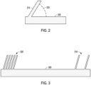
- the mold has at least one substantially flat surface and at least one of the features has a side that forms an acute angle with the mold.
- the acute angle can range from about 10 degrees to about 89 degrees, about 20 degrees to about 60 degrees, or less than, equal to, or greater than about 10 degrees, 15, 20, 25, 30, 35, 40, 45, 50, 55, 60, 65, 70, 75, 80, 85, or about 89 degrees.
- Figure 2 shows a mold (200) having a feature (210) with an acute angle (220) relative to a flat surface on the mold.
- the features can have a height: width aspect ratio from about 2:1 to about 10:1, about 3:1 to 10:1, about 4:1 to about 10:1, about 5:1 to about 10:1 about 6:1 to about 10:1, about 7:1 to about 10:1, about 9:1 to about 10:1, or any range or sub-range between these values.
- the features can have a height: width aspect ratio of about 2:1, about 3:1, about 4:1, about 5:1, about 6:1, about 7:1, about 8:1, about 9:1, about 10:1, or any range or sub-range between these values.
- the features can have a width: height aspect ratio from about 2:1 to about 10:1, about 3:1 to 10:1, about 4:1 to about 10:1, about 5:1 to about 10:1 about 6:1 to about 10:1, about 7:1 to about 10:1, about 9:1 to about 10:1, or any range or sub-range between these values.
- the features can have a width: height aspect ratio of about 2:1, about 3:1, about 4:1, about 5:1, about 6:1, about 7:1, about 8:1, about 9:1, about 10:1, or any range or sub-range between these values.
- the height of a feature can be from about 0.05 microns to about 30 microns, about 0.5 microns to about 25 microns, about 1 micron to about 22 microns, about 2 microns to about 20 microns, about 3 microns to about 18 microns, about 4 microns to about 16 microns, about 5 microns to about 14 microns, about 6 microns to about 12 microns, or any range or sub-range in between these values.
- the height of a feature can be about 0.05 microns, 1 microns, about 2 microns, about 3 microns, about 4 microns, about 5 microns, about 6 microns, about 7 microns, about 8 microns, about 9 microns, about 10 microns, about 11 microns, about 12 microns, about 13 microns, about 14 microns, about 15 microns, about 16 microns, about 17 microns, about 18 microns, about 19 microns, about 20 microns, about 21 microns, about 22 microns, about 23 microns, about 24 microns, about 25 microns, or any range or sub-range in between these values.
- the width of a feature can be from about 0.05 microns to about 30 microns, about 0.5 microns to about 25 microns, about 1 micron to about 22 microns, about 2 microns to about 20 microns, about 3 microns to about 18 microns, about 4 microns to about 16 microns, about 5 microns to about 14 microns, about 6 microns to about 12 microns, or any range or sub-range in between these values.
- the width of a feature can be about 0.05 microns to about 1 microns, about 2 microns, about 3 microns, about 4 microns, about 5 microns, about 6 microns, about 7 microns, about 8 microns, about 9 microns, about 10 microns, about 11 microns, about 12 microns, about 13 microns, about 14 microns, about 15 microns, about 16 microns, about 17 microns, about 18 microns, about 19 microns, about 20 microns, about 21 microns, about 22 microns, about 23 microns, about 24 microns, about 25 microns, or any range or sub-range in between these values.
- the depth of a feature can be from about 0.05 microns to about 30 microns, 0.5 microns to about 25 microns, about 1 micron to about 22 microns, about 2 microns to about 20 microns, about 3 microns to about 18 microns, about 4 microns to about 16 microns, about 5 microns to about 14 microns, about 6 microns to about 12 microns, or any range or sub-range in between these values.
- the depth of a feature can be about 0.05 microns, 1 micron, about 2 microns, about 3 microns, about 4 microns, about 5 microns, about 6 microns, about 7 microns, about 8 microns, about 9 microns, about 10 microns, about 11 microns, about 12 microns, about 13 microns, about 14 microns, about 15 microns, about 16 microns, about 17 microns, about 18 microns, about 19 microns, about 20 microns, about 21 microns, about 22 microns, about 23 microns, about 24 microns, about 25 microns, or any range or sub-range in between these values.
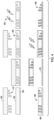
- the features are arranged in a periodic pattern. In some embodiments, the features are randomly arranged. In some embodiments, the features are arranged in a non-periodic pattern. In some embodiments, the features on the mold can be arranged such that portions of the mold have a high areal density of features spaced closely together and another portion of the mold with a pattern that does not contain any features or contains relatively few features that are spaced far apart relative to the feature size.
- Figure 3 illustrates a portion of the mold (300) with a high density of features (320) spaced closely together and a portion of the mold that has relatively few features (310) that are spaced far apart relative to the feature size.
- the separation between any two features can be from about 0.05 microns to about 1000 microns, about 5 microns to about 900 microns, about 10 microns to about 800 microns, about 20 microns to about 700 microns, about 50 microns to about 600 microns, about 75 microns to about 500 microns, about 100 microns to about 400 microns, or any range or sub-range in between these values.
- the separation between any two features can be about 0.05 microns, about 1 micron, about 5 microns, about 10 microns, about 15 microns, about 25 microns, about 35 microns, about 45 microns, about 55 microns, about 65 microns, about 75 microns, about 85 microns, about 95 microns, about 105 microns, about 115 microns, about 125 microns, about 135 microns, about 145 microns, about 155 microns, about 165 microns, about 175 microns, about 185 microns, about 195 microns, about 205 microns, about 215 microns, about 225 microns, about 235 microns, about 245 microns, about 255 microns, about 265 microns, about 275 microns, about 285 microns, about 295 microns, about 305 microns, about 315 microns, about 325 microns, about 335 microns,
- the imprinting comprises residual-free imprint lithography. Residual free imprinting can be based on adjusting surface energies/tensions of template, substrate, inks, and adjusting ink concentration and coating speed
- the imprinting creates imprinted features in the template substantially corresponding in shape and position to the features on the mold.
- the imprinting can create negative features in the template that correspond to the size and positions of the features on the mold.
- Planarizing a template with imprinted features can be accomplished by spin coating the nanoparticulate ink so that it substantially fills the imprinted features in the template.
- the method can further include a first annealing of the imprinted template.
- the first annealing can include heating, microwave irradiation, visible light irradiation, infra-red irradiation, and ultraviolet irradiation.
- the light source can be constant or the electromagnetic radiation can be deployed through a pulsed light source that delivers intense pulses of light.
- the annealing includes heating at temperatures of up to 100 °C, 200 °C, 300 °C, 400 °C, 500 °C, 600 °C, 700 °C, 800 °C, 900 °C, or 1000 °C, or any range or sub-range in between.
- the annealing is conducted at temperatures of 100 to 500 °C for a period of 5 minutes to 2 hours. In some embodiments, the annealing is conducted at temperatures between 100 °C to 1000 °C for a period of 5, 10, 15, 20, 25, 30, 40, 50, 60, 70, 80, 90, 100, 110, or 120 minutes, or any range or sub-range in between these values.
- the method includes removing the template or imprinted template from the substrate.
- Removing the template or imprinted template can include dissolution, calcination, or irradiation with microwave irradiation, visible light, infra-red radiation, or ultraviolet radiation.
- a second annealing of the substrate and nanoparticulate ink features can be performed under the conditions set forth herein.
- the first annealing dries/fuses the particles in the template.
- the second annealing promotes binding and adhesion to the substrate and between the nanoparticles.
- a method of manufacturing a textured surface includes disposing a template on a substrate, imprinting the template with a mold comprising a plurality of features that penetrate the template to form an imprinted template, planarizing the imprinted template with a nanoparticulate ink, annealing the nanoparticulate ink, removing the imprinted template.
- the imprinting creates imprinted features in the template substantially corresponding in shape and position to the features on the mold
- the nanoparticulate ink substantially fills the imprinted features in the template
- the nanoparticulate ink comprises an indium tin oxide, a titanium dioxide, an aluminum oxide, a silicon dioxide, a metal oxide, a metal nitride, a metal carbide, a metal oxynitride, a metal oxycarbide, a metal boride, a metal silicide, or combinations thereof.
- Methods of manufacturing a textured surface using a transfer print master shares many similarities with the method described herein. Any of the materials, methods, and techniques used above can be used in the following manufacturing method as well.
- a method of manufacturing a textured surface includes planarizing an imprinted template with a nanoparticulate ink to form a transfer print master and contacting the transfer print master with a substrate.
- the composition of the nanoparticulate ink and the substrate can be as set forth herein.
- the transfer print master can have any composition that is suitable for the template or imprinted template as set forth herein.
- the contacting comprises a sheet-based or roll-to-roll transfer process.
- the method can further include disposing a template on a first substrate, imprinting the template with a mold with a plurality of features that penetrate the template to form an imprinted template.
- the method further includes removing the transfer print master to provide a plurality of features disposed on the second substrate. Removing of the transfer print master can be accomplished by, for example, include dissolution, calcination, or irradiation with microwave irradiation, visible light, infra-red radiation, or ultraviolet radiation. In some cases the light may be pulsed.
- the surface of the template comprises a hard coat.
- the hard coat can include silicas, perfluoropolyethers, fluoro-containing acrylates, epoxides, fluoro-modified silica materials, or mixtures of thereof.
- the imprinted template comprises a crosslinked material.
- the template comprises a polymeric resin.
- the template can comprise any of the materials described herein.
- the imprinting can create a negative feature in the template that corresponds to the size and positions of the features on the mold. Planarizing a template with imprinted features can be accomplished by spin coating the nanoparticulate ink so that it substantially fills the imprinted features in the template.
- the imprinting includes residual-free imprint lithography.
- the imprinting, with or without residual-free imprint lithography can create imprinted features in the imprinted template substantially corresponding in shape and position to the features on the mold.
- the nanoparticulate ink substantially fills the imprinted features in the imprinted template.
- the nanoparticulate ink can include an indium tin oxide, a titanium dioxide, an aluminum oxide, a silicon dioxide, a metal oxide, a metal nitride, a metal carbide, a metal oxynitride, a metal oxycarbide, a metal boride, a metal silicide, or combinations thereof.
- the method further includes annealing the substrate.
- the annealing can be performed using any of the methods and conditions already set forth herein.
- the annealing includes heating, microwave irradiation, visible light irradiation, infra-red irradiation, and ultraviolet irradiation.
- Figure 4 shows mold (400) having a plurality of features (410), a substrate (420) and a template (430).
- imprinted features (440) in the template substantially correspond in shape and position to the features on the mold.
- the imprinted template can be planarized with nanoparticulate ink (450) to substantially fill the imprinted features with the nanoparticulate ink (460) and to form the transfer print master (465).
- the transfer print master can contact second substrate (470), and after removing of the transfer print master, the second substrate has features (480) disposed on it composed of nanoparticulate material from the nanoparticulate ink.
- the transfer print master (465) and the nanoparticulate ink (460) are annealed prior to contacting the second substrate (470).
- the template can comprise a material that is transparent to the irradiation used to heat, anneal the structure, or both, without substantially heating the transfer print master.
- An article of manufacture that includes a textured surface can be formed by any of the methods set forth herein.
- articles that can be made using the methods described herein include, without limitation, a lens, a flat lens, a meta lens, a display, a flexible display, a touch panel, a sensor surface, a shielding foil, and blaze gratings.
- the article can optionally be optically transparent.
- the article can be optically transparent to electromagnetic radiation having a wavelength through the visible and near infra-red spectrum (e.g., in a range of from about 400 nm to about 1400 nm.
- the article can be, or can be a component, of a device such as a virtual reality device or an augmented reality device.
- the article can be a component of a virtual reality or augmented reality lens, glasses, or goggles.
- a method of manufacturing a textured surface includes disposing a template on a first substrate, imprinting the template with a mold comprising a plurality of features that penetrate the template to form an imprinted template, planarizing the imprinted template with a nanoparticulate ink to form a transfer print master, annealing the nanoparticulate ink, contacting the transfer print master with a second substrate, and removing the transfer print master to provide a plurality of features disposed on the second substrate.
- the imprinting creates imprinted features in the template substantially corresponding in shape and position to the features on the mold
- the nanoparticulate ink substantially fills the imprinted features in the template
- the nanoparticulate ink comprises an indium tin oxide, a titanium dioxide, an aluminum oxide, a silicon dioxide, a metal oxide, a metal nitride, a metal carbide, a metal oxynitride, a metal oxycarbide, a metal boride, a metal silicide, or combinations thereof.
- the features deposited using the methods described herein can result in structures that contain residual nano-porosity.
- Such porosity exists in films coated on a surface from the nanoparticle based ink, in features that are directly printed onto a substrate and also in features prepared within a master for subsequent transfer to a substrate or recovery of isolated structures.
- porosity can result when using inks containing only nanoparticle dispersions and also in inks containing both nanoparticles and sol-gel type precursors that yield a desired product or binder that is incorporated into the features or other binder materials.
- such residual porosity is desirable, e.g., for ion transport through a sensor or battery electrode.
- residual porosity is deleterious in terms of structure properties, performance mechanical stability, shrinkage, or both, during calcination.
- the deposition includes the use of chemical vapor deposition (CVD) to deposit materials within the pores of the features described herein with a controlled amount, composition, thickness, or any combination of these properties.
- CVD chemical vapor deposition
- the deposition includes the use of atomic layer deposition (ALD) to deposit materials within the pores of the features described herein with a controlled amount, composition, thickness, or any combination of these properties.
- ALD atomic layer deposition
- the CVD or ALD depositions can deposit materials of substantially the same composition as the porous features or compositions that differ from the porous features.
- the ALD process can enhance mechanical stability of the printed patterns and to the structures created within the mold prior to transfer or mold removal, which can enable easier pattern transfer.
- ALD, CVD, or both can be used to apply an adhesion layer (of the same or different composition as the composition of the features to be patterned) to the structure to be transferred.
- ALD, CVD, or both can also be used to enhance adhesion of the features described herein to the substrate.
- ALD, CVD, or both can be used to reduce the surface roughness of the features described herein.
- the ALD process described herein can be applied to structures made by conventional NIL (nanoimprint lithography) printing with metal oxide inks.
- NIL noise lithography
- the structures made by the NIL printing process laid out in Kothari, R ; Beaulieu, MR; Hendricks, NR; Li, SK; Watkins, JJ, Chemistry of Materials Volume: 29 Issue: 9 Pages: 3908-3918 can be treated with the ALD process described herein.
- ALD atomic layer deposition
- a surface or substrate is exposed, sequentially, to a first reactant and a second reactant.
- the first and second reactants are deposited in a non-overlapping way.
- the deposition of a reactive substance, such as a first reactant, on a surface is limited by the amount of reactive sites on the surface. Once all of the reactive sites have been consumed, no further reaction (e.g., growth in layer thickness or filling of pores) can occur until additional reactive substance is added. Any remaining first reactant molecules can be flushed away prior to addition and deposition of a second reactant. Thus, after deposition of a first reactant, the second reactant is deposited.
- a single ALD cycle includes depositing a first reactant, optionally flushing any excess first reactant, depositing a second reactant deposition, and optionally flushing any excess second reactant. Successive cycles of this process can result in fine control of the thickness of the deposited layer or the amount of porosity reduced.
- the depositions can be carried out to impart various reductions in porosity ranging from thin surface coatings of the pores to substantially filling the pores.
- Such depositions can be conducted within films coated from the nanoparticle base ink, within freestanding printed features, or within nanoparticle compositions contained within the features of a master mold.
- Such depositions can be conducted before or after calcination (curing or annealing) of coated or printed films and features.
- a spatial ALD process can be used.
- the reagents first reactant and second reactant
- the substrate can be moved relative to the ALD head or the ALD head is moved relative to the substrate.
- Spatial ALD can be used for roll-to-roll processing of the features.
- a method of manufacturing a textured surfaces includes performing at least one cycle of atomic layer deposition (ALD) on the imprinted features, wherein the ALD comprises depositing a first reactant and a second reactant, wherein the first reactant comprises MX y , MR y , M(NR) y , M(OR) y , MX y R z , MX y (NR) z , MX y (OR) z , MCp 2 , or combinations thereof and the second reactant comprises water or oxygen.
- Each y and z is independently an integer from 2 to 8.
- Each X is independently F, Cl, Br, or I.
- Each R is independently hydrogen or a substituted or unsubstituted C 1-20 alkyl, and Cp is a substituted or unsubstituted cyclopentadienyl.
- Suitable metals can include Al, Ti, Si, Cu, Pd, Ni, Ru, Ta, Zr, Zn, In, Hf, Sn, Pt, and combinations thereof.
- the metal is Ti.
- the first reactant is tetrakis(dimethylamino)titanium (TDMAT), with the following structure:
- Suitable second reactants include water, oxygen, and ozone.
- the second reactant is water.
- the second reactant reacts with the first reactant on the surface, in the pores, or both, of the one or more features.
- reaction of TDMAT with water produces TiO 2 on the one or more features, the pores, or both, of the one or more features.
- the ALD can be conducted at a temperature of about 100 °C to about 800 °C, about 200 to 800 °C, 200 to 700 °C, 200 to 600 °C, 200 to 500 °C, 200 to 400 °C, or 200 to 300 °C.
- the ALD is can be conducted at a temperature of about 100 °C, about 200 °C, 250 °C, 300 °C, 350 °C, 400 °C, 450 °C, 500 °C, 550 °C, 600 °C, 650 °C, 700 °C, 750 °C, 800 °C, or any range between these values. In some embodiments, the ALD is conducted at a temperature of 250 °C.
- the thickness of the deposited material after each ALD cycle can be about 0.01 ⁇ to 1.0 ⁇ , 0.05 ⁇ to 1.0 ⁇ , 0.1 ⁇ to 0.9 ⁇ , 0.1 ⁇ to 0.8 ⁇ , 0.1 ⁇ to 0.7 ⁇ , 0.2 ⁇ to 0.7 ⁇ , 0.2 ⁇ to 0.6 ⁇ , or any range or sub-range between these values.
- the thickness of the deposited material after each ALD cycle can be 0.01 ⁇ , 0.05 ⁇ , 0.2 ⁇ , 0.3 ⁇ , 0.4 ⁇ , 0.5 ⁇ , 0.6 ⁇ , 0.7 ⁇ , 0.8 ⁇ , 0.9 ⁇ , 1.0 ⁇ , or any range between these values.
- the number of ALD cycles used can be about from about 1 to 5000 cycles, 1 to 4000 cycles, 1 to 3000 cycles, 1 to 2000 cycles, 1 to 1000 cycles, 1 to 500 cycles, 1 to 400 cycles, 1 to 300 cycles, 1 to 200 cycles, 1 to 100 cycles, 1 to 90 cycles, 1 to 80 cycles, 1 to 70 cycles, 1 to 60 cycles, 1 to 50 cycles, 1 to 40 cycles, 1 to 30 cycles, 1 to 20 cycles, or any range between these values.
- the number of ALD cycles can be 1, 2, 3, 4, 5, 6, 7, 8, 9, 10, 15, 20, 25, 30, 35, 40, 45, 50, 55, 60, 65, 70, 75, 80, 85, 90, 100, 110, 120, 130, 140, 150, 160, 170, 180, 190, 200, 220, 240, 260, 280, 300, 320, 340, 360, 380, 400, 420, 440, 460, 480, 500, or any range or sub-range between these values.
- the textured surface can be heated at a temperature of about 200 °C to 1000 °C, 200 °C to 900 °C, 200 °C to 800 °C, 200 °C to 700 °C, 200 °C to 600 °C, 200 °C to 500 °C, 400 °C to 800 °C, or any range between these values.
- the textured surface can be heated at a temperature of about 200 °C, 250 °C, 300 °C, 350 °C, 400 °C, 450 °C, 500 °C, 550 °C, 600 °C, 650 °C, 700 °C, 750 °C, 800 °C, 850 °C, 900 °C, 950 °C, 1000 °C, or any range or sub-range between these values.
- the heating can be performed for about 1 to 12 hours, 1 to 11 hours, 1 to 10 hours, 1 to 9 hours, 1 to 8 hours, 1 to 7 hours, 1 to 6 hours, 1 to 5 hours, 1 to 4 hours, 1 to 3 hours, 1 to 2 hours, 2 to 6 hours, 3 to 5 hours, or any range between these values. In some embodiments, the heating can be performed for about 1 hour, 2 hours, 3 hours, 4 hours, 5 hours, 6 hours, 7 hours, 8 hours, 9 hours, 10 hours, 11 hours, 12 hours, or any range or sub-range between these values.
- a feature after ALD treatment, can exhibit shrinkage from about 1% to 15%, 1% to 4%, 1% to 13%,1% to 12%,1% to 11%, 1% to 10%, 1% to 9%, 1% to 8%, 1% to 7%, 1% to 6%, 1% to 5%, 1% to 4%, or 1% to 3%.
- a feature after ALD treatment, can exhibit shrinkage from 1%, 1.5%, 2%, 2.5%, 3%, 3.5%, 4%, 4.5%, 5%, 5.5%, 6%, 6.5%, 7%, 7.5%, 8%, 8.5%, 9%, 9.5%, 10%, or any range or sub-range between these values.
- the structure can be annealed through exposure to electromagnetic radiation.
- the electromagnetic radiation can be delivered through microwave irradiation, visible light irradiation, infra-red irradiation, and ultraviolet irradiation.
- the light source can be constant or the electromagnetic radiation can be deployed through a pulsed light source that delivers intense pulses of light.
- a feature after ALD treatment, can exhibit a refractive index of from about 1.2 to 4.0, 1.2 to 3.8, 1.2 to 3.6, 1.2 to 3.4, 1.2 to 3.2, 1.2 to 3.0, 1.2 to 2.8, 1.2 to 2.6, 1.2 to 2.4, 1.2 to 2.2, 1.2 to 2.0, 1.2 to 1.8, 1.2 to 1.6, 1.2 to 1.4, or any range or sub range in between these values.
- a feature after ALD treatment, can exhibit a refractive index of about 1.0, 1.1, 1.2, 1.3, 1.4, 1.5, 1.6, 1.7, 1.8, 1.9, 2, 2.1, 2.2, 2.3, 2.4, 2.5, 2.6, 2.7, 2.8, 2.9, 3, 3.1, 3.2, 3.3, 3.4, 3.5, 3.6, 3.7, 3.8, 3.9, 4.0, or any range or sub-range in between these values.
- the ALD treatment described herein can fill the pores in the features described herein and minimizes shrinkage in the printed or transferred features during post processing, annealing, or both. In some embodiments, the ALD fills pores in the features with TiO 2 . In some embodiments, the features have a shrinkage of about 1 to 15% after the features are heated at a temperature of about 200 °C to 1000 °C or the features are exposed to light. In some embodiments, the features have a refractive index of about 1.2 to 4.0 after the features are heated at a temperature of about 200 °C to 1000 °C or the features are exposed to light.
- the refractive index of the article can be adjusted or tuned.
- tuning or adjustment using ALD can be used to correct errors in manufacturing e.g., bringing the refractive index to a desired value not present in the formed article.
- an ALD process can also be used to tune the refractive index value in an article that is intentionally formed to have a refractive index value that is below a predetermined and desirable refractive index. Imprinting alone may not provide the accuracy in achieving a predetermined refractive index value. However, a precise predetermined refractive index value may be achieved by using imprinting to achieve an article with a refractive index value that is within about 10% of the predetermined refractive index value, or about 9%, 8%, 7%, or about 6%. ALD can then be used to fine tune the refractive index value to be within about 5%, 4%, 3%, 2%, 1%, 0.5%, 0.05%, or about 0.01% of the predetermined value or at the predetermined value.
- ALD can fine tune the refractive index of the article by reducing the porosity of the article.
- the porosity can result from unintentionally created porosity formed during the imprinting process.
- porosity in the article can be intentionally induced in the article, for example, the nanoparticles can be functionalized with an organic ligand, which induces porosity in the article. Porosity can further be tuned by controlling the particle size distribution of the nanoparticles in the ink, spin coating time, or through the selection and use of binders.
- ALD can be used to fill the intentionally created pores to tune the refractive index.
- the film as prepared by spin coating from the NP-based ink exhibits a refractive index (RI) of 1.82.
- the NP-based ink contained 1,2-propanediol, methanol, isopropanol, and titanium diisopropoxide bis(acetylacetonate). After heating to 250 °C the film exhibits a refractive index of approximately 1.86. After 25 deposition cycles the film exhibits a RI of 2.25. Lateral shrinkage of TiO 2 films coated from the TiO 2 NP ink and TiO 2 coated films prepared using the NP based ink followed by deposition of TiO 2 within the pores by ALD were compared after heating to 475 °C for 4 hours.
- the films without ALD treatment exhibited a shrinkage of 18.8% whereas the films treated with ALD for 25 cycles and for 150 cycles exhibited shrinkages of 6.8 and 3.7% respectively.
- Porosity can be calculated from refractive index.
- Films without ALD treatment exhibited positions of 3 1. 1% and 28.1% before and after heating to 475 °C for 4 hours respectively whereas films subject to 25 cycles of ALD exhibited porosities of 9.0 % and 6.9% before and after heating to 475 °C for 4 hours respectively.
- Tables 3 and 4 show the data associated with the change in refractive index percent of a substrate after ALD of TiO 2 .
- Table 3. Comparison of the Refractive Index (n D ) as function of number of ALD cycles, with and without ALD of TiO 2 after 4 hours of treating the sample at 475 °C.
- the ALD treatment can reduce the porosity of nanoparticulate ink films or features described herein.
- Heat treatment results in smaller changes in porosity for ALD-treated samples compared to NP-only (nanoparticulate) samples. Table 5. Comparison of the change in porosity as a function of ALD cycles. Samples were heated to 475 °C and held at that temperature for 4 hours. # of ALD Cycles Shrinkage, % Before Heating After Heating 0 31.1 28.1 25 9.0 6.9 50 8.1 6.5 150 8.5 6.9 380 8.5 6.9
- TiO 2 NPs in 1,2-propanediol were purchased from US Research Nanomaterials Inc.
- TiO 2 precursor, tetrakis(dimethylamino)titanium (TDMAT), and aluminum oxide (Al 2 O 3 ) precursor, trimethylaluminum (TMA), were purchased from Cambridge NanoTech.
- Titanium diisopropoxide bis(acetylacetonate), 75% in isopropanol, and photoinitiator 2,2-dimethoxy-2-phenylacetophenone (DMPA), 99% was purchased from Sigma Aldrich.
- Sylgard 184 polydimethyl siloxane, PDMS was purchased from Ellsworth Adhesives.
- Fluorolink MD700 was purchased from Cornerstone Technology, LLC. ST505 PET web was purchased from Tekra. Silicon substrates were purchased from Nova Electronics. Quartz substrates were purchased from ChemGlass. All materials were used without further purification.
- Nanoparticle dispersions were prepared by diluting the stock TiO 2 nanoparticles from 20 wt% to between 2.5 and 10 wt% using methanol. The dispersions were then sonicated for 5 minutes. After sonication, 10% titanium diisopropoxide bis(acetylacetonate) or tetraethylorthosilicate (TEOS) was added to the dispersions (10% solids with respect to the mass of TiO 2 NPs), and the dispersions were sonicated again for 5 minutes.
- TEOS tetraethylorthosilicate
- stamps were prepared by pouring PDMS prepolymer onto fluorinated silicon wafers containing various nanopatterns. After curing, the PDMS stamps are easily removed and can be used and reused in solvent-assisted NIL. The diluted TiO 2 dispersions were spin coated at 3000 rpm under 5% RH for 5-30 seconds and then a PDMS stamp was placed carefully on top of the film. After several minutes on a 50 °C hotplate, the PDMS stamp was removed, revealing imprinted TiO 2 .
- HAR high aspect ratio
- Fluorinated silicon masters containing HAR vias were spin coated with Fluorolink MD700 prepolymer containing 2% DMPA (with respect to prepolymer weight) and then placed facedown onto a cured NOA60-coated piece of PET.
- the entire assembly was placed in a Nanonex imprinting tool (NX-2600BA), pumped down for 2 minutes, and then imprinted and UV-cured at 10 psi for 15 minutes. After separation, the fluoropolymer replica mold containing pillars was adhered to a Si wafer with a layer of NOA60 using the Nanonex to ensure a flat, smooth surface.
- NX-2600BA Nanonex imprinting tool
- composite PDMS stamps were prepared in order to improve transfer of the HAR features.
- the fabrication of composite stamps briefly includes mixing VS, TCS, Pt-DVS, and MCP in appropriate amounts, spin coating a layer onto the replica master, curing on a hotplate, and then backing with Sylgard 184. After curing, the HPDMS stamps were used to imprint the TiO 2 NP-based ink.
- the imprinted HAR pillar features were subjected to NIR irradiation (Adphos 126-125 NIR dryer) through the stamp before separation.
- Top-down and cross-sectional films and nanostructures were analyzed by scanning electron microscopy using a FEI Magellan 400 FESEM. Surface roughness was measured using an atomic force microscope (Veeco Dimension 3100). Composition as a function of film depth was characterized by X-ray photoelectron spectroscopy (XPS) using a Quantum 2000 Scanning ESCA microprobe (Physical Electronics, Inc.) with Al-K ⁇ radiation (1486.6 eV).
- XPS X-ray photoelectron spectroscopy
- Nanostructures and thin films were prepared by spin coating a NP dispersion onto a Si substrate and either imprinted or allowed to fully dry before ALD. For each ALD treatment, samples were deposited onto NP-based films as well as onto bare silicon, for reference.
- Table 6 shows the expected thicknesses for the different depositions onto bare Si, which were calculated according to the growth rate of 0.4 ⁇ /cycle provided by Cambridge NanoTech. Both the measured refractive indices and thicknesses match well with the expected results. The decrease in refractive index with number of cycles is expected and is due to discontinuous film formation with only a few deposition cycles. The NP films were characterized before and after each ALD treatment. Table 6. TiO 2 Deposition onto Bare Si # of cycles Expected thickness, nm Measured thickness on bare Si, nm Measured refractive index on bare Si 380 15 15 2.5 150 6 6 2.46 50 2 2.3 2.40 25 1 1.4 2.32
- the thickness and refractive index of planar TiO 2 NP films were measured after spin coating and after a 250 °C heat treatment as controls since the deposition takes place at 250 °C.
- the refractive index of the as-spun film increases from 1.82 to 1.86, and the film thickness decreases from 48 to 44 nm after a 2-hour 250 °C heat treatment. These slight changes can be attributed to a mild densification of the NP film.
- the measured total film thickness is 72 nm and the refractive index is 2.26, however after just 25 cycles, there is a negligible change in film thickness accompanied by an approximately 24% increase in refractive index.
- the full refractive index as a function of wavelength for 50 cycles of ALD emphasizes the dramatic, near-bulk values that can achieved by a short ALD process step. The results imply that the intrinsic porosity of the NP films is being decreased by ALD, which can also be observed from the change in film surface morphology with increasing ALD cycles.
- the porosity of the NP films was calculated after spin after 0, 25, 50, 150, and 380 ALD cycles before and after a 4-hour 475°C heat treatment, as shown in Table 7. Table 7. Porosity Calculated from Lorentz-Lorenz Equation. # ALD cycles Porosity, % Before heating After heating 0 31.1 28.1 25 9.0 6.9 50 8.1 6.5 150 8.5 6.9 380 8.5 6.9
- the porosity of the untreated sample decreases, but remains close to 30%.
- a dramatic decrease in the porosity by over 20% was observed, corresponding to an increased refractive index.
- the porosity decreases by just 1.6%, compared to 3% for the untreated sample.
- patterned structures with ARs greater than 1 were generated.
- the pillars were produced by direct patterning, requiring no etching or resist-removal steps and can be scaled to wafer-based production.
- the HAR pillars require a through-stamp annealing treatment before stamp removal to encourage enough binding between the NPs to ensure the pillars do not break during stamp removal.
- the solvent was allowed to dry out on a hotplate and then the substrate-stamp assembly was subjected to 20s of NIR irradiation.
- the pillars can be effectively patterned over large areas.
- a UV-curable polymer, NOA60 was imprinted.
- NOA60 a UV-curable polymer
- the diameter of the imprinted NOA60 pillars is measured to be 140 ⁇ 5 nm at the top of the pillar and the height to be 1.1 ⁇ m, resulting in an HAR of 7.9.
- the imprinted TiO 2 from the same section measures 130 ⁇ 4 nm in diameter and 815 nm in height, resulting in an HAR of 6.3.
- the measured shrinkage of the NP pillars with respect to the master is less than 10% in diameter, however, in height the shrinkage is 26%.
- the shrinkage results from the solvent-assisted imprinting technique; the solvent-dispersed NPs fill the PDMS stamp by capillary forces and then the solvent diffuses through the stamp, resulting in a underfilled mold volume.
- the master mold could be fabricated to include the compensation for shrinkage.
- HAR TiO 2 pillars as-imprinted show the same pillar area after 50 cycles of TiO 2 ALD. No obvious change in the structures is observed, indicating that the deposited TiO 2 is not simply deposited on the surface.
- One observed change between the HAR pillars before and after ALD is the slight increase in HAR after ALD, which most likely arises from mild shrinkage from heating during ALD (250°C).
- the ability to tune the refractive index over a range of values opens the door to situations requiring precise index tailoring, matching, and/or grading.
- the films were prepared by spin coating TiO 2 NP films for five seconds, and then further dried on a hotplate at 60 °C for two minutes, which mimics the conditions used to generate nanopatterns through solvent-assisted NIL. It should be noted that this results in a slightly lower starting refractive index value (0 cycles ALD). This can be attributed to differences in NP packing; films spin-coated until complete solvent removal pack more densely and have a slightly higher value (1.82 versus 1.77).
- the refractive index (n D ) increases linearly with the number of ALD cycles between 2 and 15, which allows access to intermediate index values, which can be used to fabricate gradient refractive index (GRIN) lenses.
- This method of tunability benefits from being completely inorganic and composed of a single material. All-inorganic materials are desirable in many applications where durability and UV-stability are concerns. Additionally, by using only TiO 2 , compatibility between the two materials is ensured.
Landscapes
- Chemical & Material Sciences (AREA)
- Engineering & Computer Science (AREA)
- General Chemical & Material Sciences (AREA)
- Chemical Kinetics & Catalysis (AREA)
- Materials Engineering (AREA)
- Mechanical Engineering (AREA)
- Metallurgy (AREA)
- Organic Chemistry (AREA)
- Physics & Mathematics (AREA)
- Inorganic Chemistry (AREA)
- Thermal Sciences (AREA)
- General Physics & Mathematics (AREA)
- Ceramic Engineering (AREA)
- Shaping Of Tube Ends By Bending Or Straightening (AREA)
- Diffracting Gratings Or Hologram Optical Elements (AREA)
- Laminated Bodies (AREA)
- Chemical Vapour Deposition (AREA)
- Application Of Or Painting With Fluid Materials (AREA)
Claims (10)
- Ein Verfahren zur Herstellung einer strukturierten Oberfläche, das Folgendes beinhaltet:Aufbringen einer nanopartikelbasierten Tinte auf ein Substrat;Prägen der Tinte mit einer Form, die eine Vielzahl von Merkmalen beinhaltet, um eine strukturierte nanopartikelbasierte Tinte zu bilden; undDurchführen mindestens eines Zyklus von Atomschichtabscheidung, ALD, auf der strukturierten nanopartikelbasierten Tinte, um Poren in der strukturierten nanopartikelbasierten Tinte zu füllen und die strukturierte Oberfläche zu bilden, wobei die ALD Folgendes beinhaltet: sequenzielles Abscheiden eines ersten Reaktanten, der MXy, MRy, M(R)y, M(NR)y, M(OR)y, MXyRz, MXy(R)z, MXy(NR)z, MXy(OR)z, MCp2 oder Kombinationen davon beinhaltet, und eines zweiten Reaktanten, der Wasser, Sauerstoff oder Ozon beinhaltet, wobeijedes y und z unabhängig eine ganze Zahl von 2 bis 8 ist;M ein Metall ist;jedes X unabhängig F, Cl, Br oder I ist;jedes R unabhängig Wasserstoff oder ein substituiertes oder unsubstituiertes C1-20-Alkyl ist;
undCp ein substituiertes oder unsubstituiertes Cyclopentadienyl ist; undim Anschluss an den mindestens einen Zyklus von ALD Behandeln der nanopartikelbasierten Tinte durch Aussetzen gegenüber elektromagnetischer Strahlung oder durch Erwärmen. - Verfahren gemäß Anspruch 1, wobei die nanopartikelbasierte Tinte Folgendes beinhaltet:Nanopartikel; undein Bindemittel.
- Verfahren gemäß Anspruch 2, wobei das Bindemittel einen Sol-Gel-Vorläufer oder ein Siloxan beinhaltet.
- Verfahren gemäß einem der Ansprüche 1 bis 3, das ferner das Unterziehen der strukturierten Oberfläche einem Erwärmen bei 200 °C bis 1000 °C oder einer elektromagnetischen Strahlung beinhaltet, wobei Merkmale des transferierten Musters eine Schrumpfung von 1 % bis 15 % aufweisen, nachdem die strukturierte Oberfläche dem Erwärmen oder der elektromagnetischen Strahlung unterzogen worden ist.
- Verfahren gemäß Anspruch 1, das ferner das Durchführen einer Vielzahl der Zyklen von Atomschichtabscheidung, ALD, beinhaltet.
- Verfahren gemäß einem der Ansprüche 1 bis 5, wobei der eine oder die mehreren Zyklen der ALD verwendet werden, um eine Brechungszahl der strukturierten Oberfläche auf einen gewünschten Wert einzustellen.
- Verfahren gemäß einem der Ansprüche 1 bis 6, wobei der eine oder die mehreren Zyklen der ALD die Schrumpfung der strukturierten Oberfläche während des anschließenden Erwärmens oder Aussetzens gegenüber elektromagnetischer Strahlung verringern.
- Verfahren gemäß einem der vorhergehenden Ansprüche, wobeidie Nanopartikeltinte ein Siliciumdioxid, ein Metalloxid, ein Metallnitrid, ein Metallcarbid, ein Metalloxynitrid, ein Metalloxycarbid, ein Metallborid, ein Metallsilicid oder Kombinationen davon beinhaltet, wobei das Metalloxid bevorzugt ein Indiumzinnoxid, ein Titandioxid oder ein Aluminiumoxid ist,und wobei der zweite Reaktant Wasser beinhaltet.
- Ein Artikel, der Folgendes beinhaltet:eine strukturierte, mit Atomschichtabscheidung behandelte Oberfläche, die eine Vielzahl von Merkmalen beinhaltet, die aus dieser hervorragen und in einem periodischen Muster angeordnet oder zufällig angeordnet sind, wobei die strukturierte Oberfläche gegenüber sichtbarem Licht optisch transparent ist;wobei die Merkmale unabhängig ein Höhe-Breite-Seitenverhältnis von 2 : 1 bis 10 : 1 aufweisen; undwobei die mit Atomschichtabscheidung behandelte Oberfläche Folgendes beinhaltet: ein Atomschichtabscheidungsreaktionsprodukt aus einem ersten Reaktanten, der MXy, MRy, M(NR)y, M(R)y, M(OR)y, MXyRz, MXy(R)z, MXy(NR)z, MXy(OR)z, MCp2 oder Kombinationen davon beinhaltet, und einem zweiten Reaktanten, der Wasser, Sauerstoff oder Ozon beinhaltet, wobeijedes y und z unabhängig eine ganze Zahl von 2 bis 8 ist;M ein Metall ist;jedes X unabhängig F, Cl, Br oder I ist;jedes R unabhängig Wasserstoff oder ein substituiertes oder unsubstituiertes C1-20-Alkyl ist;
undCp ein substituiertes oder unsubstituiertes Cyclopentadienyl ist. - Artikel gemäß Anspruch 9, wobei der Artikel eine Linse, ein Display, ein flexibles Display, ein Tastfeld, eine Sensoroberfläche, eine Abschirmfolie, eine Metalinse, ein Lichtfelddisplay, eine flache Linse, ein Blazegitter, ein Virtual-Reality-Gerät oder ein Augmented-Reality-Gerät beinhaltet.
Applications Claiming Priority (2)
| Application Number | Priority Date | Filing Date | Title |
|---|---|---|---|
| US201762565703P | 2017-09-29 | 2017-09-29 | |
| PCT/US2018/053442 WO2019067912A1 (en) | 2017-09-29 | 2018-09-28 | FORMATION OF PATTERNS ON COMPLEX METAL OXIDE STRUCTURES |
Publications (5)
| Publication Number | Publication Date |
|---|---|
| EP3687785A1 EP3687785A1 (de) | 2020-08-05 |
| EP3687785A4 EP3687785A4 (de) | 2021-07-07 |
| EP3687785C0 EP3687785C0 (de) | 2025-04-02 |
| EP3687785B1 true EP3687785B1 (de) | 2025-04-02 |
| EP3687785B8 EP3687785B8 (de) | 2025-05-07 |
Family
ID=65903209
Family Applications (1)
| Application Number | Title | Priority Date | Filing Date |
|---|---|---|---|
| EP18862056.1A Active EP3687785B8 (de) | 2017-09-29 | 2018-09-28 | Strukturierung von komplexen metalloxidstrukturen |
Country Status (5)
| Country | Link |
|---|---|
| US (2) | US12099294B2 (de) |
| EP (1) | EP3687785B8 (de) |
| JP (3) | JP7267624B2 (de) |
| KR (3) | KR102779109B1 (de) |
| WO (1) | WO2019067912A1 (de) |
Families Citing this family (19)
| Publication number | Priority date | Publication date | Assignee | Title |
|---|---|---|---|---|
| US12099294B2 (en) | 2017-09-29 | 2024-09-24 | University Of Massachusetts | Patterning of complex metal oxide structures |
| DE102019101346A1 (de) * | 2019-01-18 | 2020-07-23 | Osram Opto Semiconductors Gmbh | Nanostempelverfahren und nanooptisches bauteil |
| US12050327B2 (en) * | 2019-06-04 | 2024-07-30 | Applied Materials, Inc. | Imaging system and method of manufacturing a metalens array |
| WO2021016354A1 (en) * | 2019-07-23 | 2021-01-28 | University Of Massachusetts | Thermal imprinting of nanostructure materials |
| US12044963B2 (en) * | 2020-01-22 | 2024-07-23 | Applied Materials, Inc. | High refractive index imprint compositions and materials and processes for making the same |
| US20210325777A1 (en) | 2020-04-20 | 2021-10-21 | Applied Materials, Inc. | Methods for increasing the refractive index of high-index nanoimprint lithography films |
| US12522920B2 (en) | 2020-08-25 | 2026-01-13 | Amo Groningen B.V. | Partial coating of intraocular lenses using spatial atomic layer deposition |
| KR20230109688A (ko) | 2020-11-18 | 2023-07-20 | 어플라이드 머티어리얼스, 인코포레이티드 | 패시베이션된 나노입자들을 갖는 임프린트 조성물들 및 이를 제조하기 위한 재료들 및 프로세스들 |
| CN116615331A (zh) * | 2020-12-18 | 2023-08-18 | 3M创新有限公司 | 结构化膜和包括结构化膜的光学制品 |
| US20220252779A1 (en) * | 2021-02-08 | 2022-08-11 | Applied Materials, Inc. | Method for amorphous, high-refractive-index encapsulation of nanoparticle imprint films for optical devices |
| JP2022170427A (ja) * | 2021-04-28 | 2022-11-10 | 東京応化工業株式会社 | パターン形成方法及び硬化性組成物の製造方法 |
| CN114371521A (zh) * | 2022-01-13 | 2022-04-19 | 天津山河光电科技有限公司 | 覆盖有反射层的超表面光学器件、光学设备及制造方法 |
| FI131505B1 (fi) * | 2022-02-22 | 2025-05-28 | Dispelix Oy | Leimasin painatuslitografiaa varten |
| US12504566B2 (en) | 2022-05-16 | 2025-12-23 | Adeia Guides Inc. | Transparent conductive diffractive gratings for optical elements of augmented reality and virtual reality displays |
| US12393029B2 (en) | 2022-03-23 | 2025-08-19 | Adeia Guides Inc. | Buried diffractive gratings for optical elements of augmented reality and virtual reality head-mounted displays |
| JPWO2024014272A1 (de) * | 2022-07-15 | 2024-01-18 | ||
| US20240076507A1 (en) * | 2022-09-01 | 2024-03-07 | Green Products & Technologies, LLC | Hydrophobic protective coating for painted and non-painted metallic surfaces |
| US20240124726A1 (en) * | 2022-10-10 | 2024-04-18 | The Trustees Of The University Of Pennsylvania | Nanoparticle Ink Based Patterning Of Inorganic Materials |
| WO2024119053A1 (en) * | 2022-12-01 | 2024-06-06 | Magic Leap, Inc. | Dummy imprinted regions |
Family Cites Families (19)
| Publication number | Priority date | Publication date | Assignee | Title |
|---|---|---|---|---|
| JPS611897U (ja) | 1984-06-11 | 1986-01-08 | 日立精工株式会社 | プリント基板加工機用の被加工物搬入、搬出装置 |
| US6967172B2 (en) * | 2002-07-03 | 2005-11-22 | Honeywell International Inc. | Colloidal silica composite films for premetal dielectric applications |
| JP2006150741A (ja) | 2004-11-29 | 2006-06-15 | Asahi Glass Co Ltd | 転写層にパターンを形成する方法 |
| US7662299B2 (en) * | 2005-08-30 | 2010-02-16 | Micron Technology, Inc. | Nanoimprint lithography template techniques for use during the fabrication of a semiconductor device and systems including same |
| US8027086B2 (en) * | 2007-04-10 | 2011-09-27 | The Regents Of The University Of Michigan | Roll to roll nanoimprint lithography |
| EP2489046A1 (de) * | 2009-10-16 | 2012-08-22 | O'Brien, Paul Gregory | Transparente und poröse leitfähige nanoverbundstoffe und herstellungsverfahren dafür |
| WO2012057706A1 (en) * | 2010-10-25 | 2012-05-03 | Nanyang Technological University | Method for micropatterning a substrate and a patterned substrate formed thereof |
| US8859050B2 (en) * | 2011-03-14 | 2014-10-14 | The Curators Of The University Of Missouri | Patterning of ultra-low refractive index high surface area nanoparticulate films |
| FR2980208B1 (fr) | 2011-09-19 | 2018-03-16 | Institut Curie | Dispositif de guidage de la migration cellulaire et methode de guidage mettant en oeuvre un tel dispositif |
| JP6101897B2 (ja) * | 2012-05-14 | 2017-03-29 | 富山県 | 焼成体の製造方法 |
| US11133118B2 (en) | 2012-05-22 | 2021-09-28 | University Of Massachusetts | Patterned nanoparticle structures |
| US20140004381A1 (en) | 2012-06-28 | 2014-01-02 | Jeffrey W. Elam | Enhanced materials and interfacial performance via infiltration |
| TWI665078B (zh) * | 2013-07-22 | 2019-07-11 | 皇家飛利浦有限公司 | 製造圖案化印模以圖案化輪廓表面之方法、供在壓印微影製程中使用之圖案化印模、壓印微影方法、包括圖案化輪廓表面之物件及圖案化印模用於壓印微影之用法 |
| KR101618436B1 (ko) * | 2014-06-02 | 2016-05-09 | 한양대학교 산학협력단 | 나노 전극층 생성 방법 |
| US10690818B2 (en) * | 2014-10-31 | 2020-06-23 | Corning Incorporated | Anti-glare substrates with a uniform textured surface and low sparkle and methods of making the same |
| BR112017013073A2 (pt) * | 2014-12-22 | 2018-01-02 | Koninklijke Philips Nv | estampa para litografia de estampagem, método de fabricação de uma estampa, uso de uma estampa, e método de impressão |
| US9827209B2 (en) * | 2015-02-09 | 2017-11-28 | Microsoft Technology Licensing, Llc | Display system |
| JP6868619B2 (ja) | 2015-10-20 | 2021-05-12 | コーニンクレッカ フィリップス エヌ ヴェKoninklijke Philips N.V. | インプリント用インク組成物、インプリント方法、光学エレメント、照明装置、光センサ及び光起電力装置 |
| US12099294B2 (en) | 2017-09-29 | 2024-09-24 | University Of Massachusetts | Patterning of complex metal oxide structures |
-
2018
- 2018-09-28 US US16/650,510 patent/US12099294B2/en active Active
- 2018-09-28 WO PCT/US2018/053442 patent/WO2019067912A1/en not_active Ceased
- 2018-09-28 JP JP2020517961A patent/JP7267624B2/ja active Active
- 2018-09-28 EP EP18862056.1A patent/EP3687785B8/de active Active
- 2018-09-28 KR KR1020247009001A patent/KR102779109B1/ko active Active
- 2018-09-28 KR KR1020207012137A patent/KR102655297B1/ko active Active
- 2018-09-28 KR KR1020257007322A patent/KR20250036963A/ko active Pending
-
2023
- 2023-03-20 JP JP2023043988A patent/JP2023100605A/ja active Pending
-
2024
- 2024-08-16 US US18/807,414 patent/US20240411224A1/en active Pending
-
2025
- 2025-05-07 JP JP2025077210A patent/JP2025109752A/ja active Pending
Also Published As
| Publication number | Publication date |
|---|---|
| KR20250036963A (ko) | 2025-03-14 |
| EP3687785B8 (de) | 2025-05-07 |
| JP7267624B2 (ja) | 2023-05-02 |
| JP2023100605A (ja) | 2023-07-19 |
| KR20240039231A (ko) | 2024-03-26 |
| US12099294B2 (en) | 2024-09-24 |
| WO2019067912A1 (en) | 2019-04-04 |
| EP3687785C0 (de) | 2025-04-02 |
| EP3687785A1 (de) | 2020-08-05 |
| US20200285145A1 (en) | 2020-09-10 |
| EP3687785A4 (de) | 2021-07-07 |
| JP2025109752A (ja) | 2025-07-25 |
| JP2020536722A (ja) | 2020-12-17 |
| US20240411224A1 (en) | 2024-12-12 |
| KR102779109B1 (ko) | 2025-03-12 |
| KR102655297B1 (ko) | 2024-04-04 |
| KR20200061389A (ko) | 2020-06-02 |
Similar Documents
| Publication | Publication Date | Title |
|---|---|---|
| EP3687785B1 (de) | Strukturierung von komplexen metalloxidstrukturen | |
| US12092953B2 (en) | Patterning of nanostructures using imprint lithography | |
| US11961628B2 (en) | Patterned nanoparticle structures | |
| US20200073234A1 (en) | Master mold for pattern transfer | |
| US8277899B2 (en) | Porous films by backfilling with reactive compounds | |
| Kothari et al. | Direct patterning of robust one-dimensional, two-dimensional, and three-dimensional crystalline metal oxide nanostructures using imprint lithography and nanoparticle dispersion inks | |
| US20080230773A1 (en) | Polymer Composition for Preparing Electronic Devices by Microcontact Printing Processes and Products Prepared by the Processes | |
| KR102569627B1 (ko) | 나노임프린트 리소그래피 프로세스 및 그것으로부터 획득가능한 패터닝된 기재 | |
| JP2019504464A (ja) | インプリント用インク組成物、インプリント方法、光学エレメント、照明装置、光センサ及び光起電力装置 | |
| CN108137310A (zh) | 制备结构化表面的方法 | |
| CN106908898A (zh) | 一种光子晶体的制备方法以及由该方法制备的光子晶体 | |
| CN101115682A (zh) | 钛氧化物粒子的分散液、钛氧化物薄膜、有机功能膜形成用溶液、有机功能膜形成基体及其制造方法 | |
| EP4625042A1 (de) | Direktmetall-nanoprägung | |
| EP2547717B1 (de) | Verfahren zur bildung einer struktur auf der oberfläche eines substrats | |
| 上原卓也 | Fabrication of Plasmonic Split-Ring Resonator Arrays for Three-dimensional Optical Metamaterials | |
| WO2015054078A1 (en) | Plasma treatment of flexographic printing surface |
Legal Events
| Date | Code | Title | Description |
|---|---|---|---|
| STAA | Information on the status of an ep patent application or granted ep patent |
Free format text: STATUS: THE INTERNATIONAL PUBLICATION HAS BEEN MADE |
|
| PUAI | Public reference made under article 153(3) epc to a published international application that has entered the european phase |
Free format text: ORIGINAL CODE: 0009012 |
|
| STAA | Information on the status of an ep patent application or granted ep patent |
Free format text: STATUS: REQUEST FOR EXAMINATION WAS MADE |
|
| 17P | Request for examination filed |
Effective date: 20200427 |
|
| AK | Designated contracting states |
Kind code of ref document: A1 Designated state(s): AL AT BE BG CH CY CZ DE DK EE ES FI FR GB GR HR HU IE IS IT LI LT LU LV MC MK MT NL NO PL PT RO RS SE SI SK SM TR |
|
| AX | Request for extension of the european patent |
Extension state: BA ME |
|
| RIN1 | Information on inventor provided before grant (corrected) |
Inventor name: WATKINS, JAMES J. Inventor name: HOWELL, IRENE R. |
|
| DAV | Request for validation of the european patent (deleted) | ||
| DAX | Request for extension of the european patent (deleted) | ||
| A4 | Supplementary search report drawn up and despatched |
Effective date: 20210608 |
|
| RIC1 | Information provided on ipc code assigned before grant |
Ipc: B32B 3/10 20060101AFI20210601BHEP Ipc: B32B 3/16 20060101ALI20210601BHEP Ipc: B32B 3/30 20060101ALI20210601BHEP Ipc: C23C 18/06 20060101ALI20210601BHEP Ipc: G03F 7/00 20060101ALI20210601BHEP Ipc: H01M 6/40 20060101ALI20210601BHEP Ipc: B82Y 30/00 20110101ALI20210601BHEP Ipc: B82Y 40/00 20110101ALI20210601BHEP |
|
| P01 | Opt-out of the competence of the unified patent court (upc) registered |
Effective date: 20230530 |
|
| STAA | Information on the status of an ep patent application or granted ep patent |
Free format text: STATUS: EXAMINATION IS IN PROGRESS |
|
| 17Q | First examination report despatched |
Effective date: 20240528 |
|
| GRAP | Despatch of communication of intention to grant a patent |
Free format text: ORIGINAL CODE: EPIDOSNIGR1 |
|
| STAA | Information on the status of an ep patent application or granted ep patent |
Free format text: STATUS: GRANT OF PATENT IS INTENDED |
|
| INTG | Intention to grant announced |
Effective date: 20241023 |
|
| GRAS | Grant fee paid |
Free format text: ORIGINAL CODE: EPIDOSNIGR3 |
|
| GRAA | (expected) grant |
Free format text: ORIGINAL CODE: 0009210 |
|
| STAA | Information on the status of an ep patent application or granted ep patent |
Free format text: STATUS: THE PATENT HAS BEEN GRANTED |
|
| AK | Designated contracting states |
Kind code of ref document: B1 Designated state(s): AL AT BE BG CH CY CZ DE DK EE ES FI FR GB GR HR HU IE IS IT LI LT LU LV MC MK MT NL NO PL PT RO RS SE SI SK SM TR |
|
| REG | Reference to a national code |
Ref country code: GB Ref legal event code: FG4D |
|
| REG | Reference to a national code |
Ref country code: DE Ref legal event code: R081 Ref document number: 602018080802 Country of ref document: DE Owner name: UNIVERSITY OF MASSACHUSETTS, WESTBOROUGH, US Free format text: FORMER OWNER: UNIVERSITY OF MASSACHUSETTS, BOSTON, MA, US |
|
| REG | Reference to a national code |
Ref country code: CH Ref legal event code: PK Free format text: BERICHTIGUNG B8 Ref country code: CH Ref legal event code: EP |
|
| REG | Reference to a national code |
Ref country code: DE Ref legal event code: R096 Ref document number: 602018080802 Country of ref document: DE |
|
| REG | Reference to a national code |
Ref country code: IE Ref legal event code: FG4D |
|
| RAP4 | Party data changed (patent owner data changed or rights of a patent transferred) |
Owner name: UNIVERSITY OF MASSACHUSETTS |
|
| U01 | Request for unitary effect filed |
Effective date: 20250423 |
|
| U07 | Unitary effect registered |
Designated state(s): AT BE BG DE DK EE FI FR IT LT LU LV MT NL PT RO SE SI Effective date: 20250429 |
|
| P04 | Withdrawal of opt-out of the competence of the unified patent court (upc) registered |
Free format text: CASE NUMBER: APP_19832/2025 Effective date: 20250425 |
|
| REG | Reference to a national code |
Ref country code: CH Ref legal event code: U11 Free format text: ST27 STATUS EVENT CODE: U-0-0-U10-U11 (AS PROVIDED BY THE NATIONAL OFFICE) Effective date: 20251001 |
|
| PG25 | Lapsed in a contracting state [announced via postgrant information from national office to epo] |
Ref country code: ES Free format text: LAPSE BECAUSE OF FAILURE TO SUBMIT A TRANSLATION OF THE DESCRIPTION OR TO PAY THE FEE WITHIN THE PRESCRIBED TIME-LIMIT Effective date: 20250402 |
|
| PG25 | Lapsed in a contracting state [announced via postgrant information from national office to epo] |
Ref country code: GR Free format text: LAPSE BECAUSE OF FAILURE TO SUBMIT A TRANSLATION OF THE DESCRIPTION OR TO PAY THE FEE WITHIN THE PRESCRIBED TIME-LIMIT Effective date: 20250703 Ref country code: NO Free format text: LAPSE BECAUSE OF FAILURE TO SUBMIT A TRANSLATION OF THE DESCRIPTION OR TO PAY THE FEE WITHIN THE PRESCRIBED TIME-LIMIT Effective date: 20250702 |
|
| PG25 | Lapsed in a contracting state [announced via postgrant information from national office to epo] |
Ref country code: PL Free format text: LAPSE BECAUSE OF FAILURE TO SUBMIT A TRANSLATION OF THE DESCRIPTION OR TO PAY THE FEE WITHIN THE PRESCRIBED TIME-LIMIT Effective date: 20250402 |
|
| PGFP | Annual fee paid to national office [announced via postgrant information from national office to epo] |
Ref country code: GB Payment date: 20250929 Year of fee payment: 8 |
|
| PG25 | Lapsed in a contracting state [announced via postgrant information from national office to epo] |
Ref country code: HR Free format text: LAPSE BECAUSE OF FAILURE TO SUBMIT A TRANSLATION OF THE DESCRIPTION OR TO PAY THE FEE WITHIN THE PRESCRIBED TIME-LIMIT Effective date: 20250402 |
|
| PG25 | Lapsed in a contracting state [announced via postgrant information from national office to epo] |
Ref country code: RS Free format text: LAPSE BECAUSE OF FAILURE TO SUBMIT A TRANSLATION OF THE DESCRIPTION OR TO PAY THE FEE WITHIN THE PRESCRIBED TIME-LIMIT Effective date: 20250702 |
|
| PG25 | Lapsed in a contracting state [announced via postgrant information from national office to epo] |
Ref country code: IS Free format text: LAPSE BECAUSE OF FAILURE TO SUBMIT A TRANSLATION OF THE DESCRIPTION OR TO PAY THE FEE WITHIN THE PRESCRIBED TIME-LIMIT Effective date: 20250802 |
|
| U20 | Renewal fee for the european patent with unitary effect paid |
Year of fee payment: 8 Effective date: 20250929 |
|
| PG25 | Lapsed in a contracting state [announced via postgrant information from national office to epo] |
Ref country code: SM Free format text: LAPSE BECAUSE OF FAILURE TO SUBMIT A TRANSLATION OF THE DESCRIPTION OR TO PAY THE FEE WITHIN THE PRESCRIBED TIME-LIMIT Effective date: 20250402 |
|
| PGFP | Annual fee paid to national office [announced via postgrant information from national office to epo] |
Ref country code: CH Payment date: 20251001 Year of fee payment: 8 |
|
| PG25 | Lapsed in a contracting state [announced via postgrant information from national office to epo] |
Ref country code: CZ Free format text: LAPSE BECAUSE OF FAILURE TO SUBMIT A TRANSLATION OF THE DESCRIPTION OR TO PAY THE FEE WITHIN THE PRESCRIBED TIME-LIMIT Effective date: 20250402 |
|
| PG25 | Lapsed in a contracting state [announced via postgrant information from national office to epo] |
Ref country code: SK Free format text: LAPSE BECAUSE OF FAILURE TO SUBMIT A TRANSLATION OF THE DESCRIPTION OR TO PAY THE FEE WITHIN THE PRESCRIBED TIME-LIMIT Effective date: 20250402 |
|
| PLBE | No opposition filed within time limit |
Free format text: ORIGINAL CODE: 0009261 |
|
| STAA | Information on the status of an ep patent application or granted ep patent |
Free format text: STATUS: NO OPPOSITION FILED WITHIN TIME LIMIT |
|
| REG | Reference to a national code |
Ref country code: CH Ref legal event code: L10 Free format text: ST27 STATUS EVENT CODE: U-0-0-L10-L00 (AS PROVIDED BY THE NATIONAL OFFICE) Effective date: 20260211 |
|
| 26N | No opposition filed |
Effective date: 20260105 |