EP3676864B1 - Hf-kompensationsschaltung und steuerung für ein kreuzgekoppeltes simo-verteilnetz - Google Patents
Hf-kompensationsschaltung und steuerung für ein kreuzgekoppeltes simo-verteilnetz Download PDFInfo
- Publication number
- EP3676864B1 EP3676864B1 EP18849592.3A EP18849592A EP3676864B1 EP 3676864 B1 EP3676864 B1 EP 3676864B1 EP 18849592 A EP18849592 A EP 18849592A EP 3676864 B1 EP3676864 B1 EP 3676864B1
- Authority
- EP
- European Patent Office
- Prior art keywords
- leg
- value
- power
- electrical
- splitter
- Prior art date
- Legal status (The legal status is an assumption and is not a legal conclusion. Google has not performed a legal analysis and makes no representation as to the accuracy of the status listed.)
- Active
Links
Images






Classifications
-
- H—ELECTRICITY
- H03—ELECTRONIC CIRCUITRY
- H03H—IMPEDANCE NETWORKS, e.g. RESONANT CIRCUITS; RESONATORS
- H03H7/00—Multiple-port networks comprising only passive electrical elements as network components
- H03H7/42—Networks for transforming balanced signals into unbalanced signals and vice versa, e.g. baluns
-
- H—ELECTRICITY
- H01—ELECTRIC ELEMENTS
- H01J—ELECTRIC DISCHARGE TUBES OR DISCHARGE LAMPS
- H01J37/00—Discharge tubes with provision for introducing objects or material to be exposed to the discharge, e.g. for the purpose of examination or processing thereof
- H01J37/32—Gas-filled discharge tubes
- H01J37/32009—Arrangements for generation of plasma specially adapted for examination or treatment of objects, e.g. plasma sources
- H01J37/32082—Radio frequency generated discharge
- H01J37/32174—Circuits specially adapted for controlling the RF discharge
- H01J37/32183—Matching circuits
-
- H—ELECTRICITY
- H01—ELECTRIC ELEMENTS
- H01J—ELECTRIC DISCHARGE TUBES OR DISCHARGE LAMPS
- H01J37/00—Discharge tubes with provision for introducing objects or material to be exposed to the discharge, e.g. for the purpose of examination or processing thereof
- H01J37/32—Gas-filled discharge tubes
- H01J37/32009—Arrangements for generation of plasma specially adapted for examination or treatment of objects, e.g. plasma sources
- H01J37/32082—Radio frequency generated discharge
- H01J37/32174—Circuits specially adapted for controlling the RF discharge
-
- H—ELECTRICITY
- H01—ELECTRIC ELEMENTS
- H01J—ELECTRIC DISCHARGE TUBES OR DISCHARGE LAMPS
- H01J37/00—Discharge tubes with provision for introducing objects or material to be exposed to the discharge, e.g. for the purpose of examination or processing thereof
- H01J37/32—Gas-filled discharge tubes
- H01J37/32431—Constructional details of the reactor
- H01J37/32798—Further details of plasma apparatus not provided for in groups H01J37/3244 - H01J37/32788; special provisions for cleaning or maintenance of the apparatus
- H01J37/32889—Connection or combination with other apparatus
-
- H—ELECTRICITY
- H01—ELECTRIC ELEMENTS
- H01J—ELECTRIC DISCHARGE TUBES OR DISCHARGE LAMPS
- H01J37/00—Discharge tubes with provision for introducing objects or material to be exposed to the discharge, e.g. for the purpose of examination or processing thereof
- H01J37/32—Gas-filled discharge tubes
- H01J37/32431—Constructional details of the reactor
- H01J37/32798—Further details of plasma apparatus not provided for in groups H01J37/3244 - H01J37/32788; special provisions for cleaning or maintenance of the apparatus
- H01J37/32899—Multiple chambers, e.g. cluster tools
-
- H—ELECTRICITY
- H01—ELECTRIC ELEMENTS
- H01P—WAVEGUIDES; RESONATORS, LINES, OR OTHER DEVICES OF THE WAVEGUIDE TYPE
- H01P5/00—Coupling devices of the waveguide type
- H01P5/12—Coupling devices having more than two ports
- H01P5/16—Conjugate devices, i.e. devices having at least one port decoupled from one other port
- H01P5/19—Conjugate devices, i.e. devices having at least one port decoupled from one other port of the junction type
-
- H—ELECTRICITY
- H03—ELECTRONIC CIRCUITRY
- H03H—IMPEDANCE NETWORKS, e.g. RESONANT CIRCUITS; RESONATORS
- H03H7/00—Multiple-port networks comprising only passive electrical elements as network components
- H03H7/46—Networks for connecting several sources or loads, working on different frequencies or frequency bands, to a common load or source
-
- H—ELECTRICITY
- H03—ELECTRONIC CIRCUITRY
- H03H—IMPEDANCE NETWORKS, e.g. RESONANT CIRCUITS; RESONATORS
- H03H7/00—Multiple-port networks comprising only passive electrical elements as network components
- H03H7/48—Networks for connecting several sources or loads, working on the same frequency or frequency band, to a common load or source
-
- H—ELECTRICITY
- H01—ELECTRIC ELEMENTS
- H01J—ELECTRIC DISCHARGE TUBES OR DISCHARGE LAMPS
- H01J2237/00—Discharge tubes exposing object to beam, e.g. for analysis treatment, etching, imaging
- H01J2237/32—Processing objects by plasma generation
- H01J2237/33—Processing objects by plasma generation characterised by the type of processing
- H01J2237/332—Coating
- H01J2237/3322—Problems associated with coating
- H01J2237/3323—Problems associated with coating uniformity
-
- H—ELECTRICITY
- H01—ELECTRIC ELEMENTS
- H01J—ELECTRIC DISCHARGE TUBES OR DISCHARGE LAMPS
- H01J2237/00—Discharge tubes exposing object to beam, e.g. for analysis treatment, etching, imaging
- H01J2237/32—Processing objects by plasma generation
- H01J2237/33—Processing objects by plasma generation characterised by the type of processing
- H01J2237/334—Etching
Definitions
- the present disclosure relates to RF systems and to distributing power between multiple power, voltage, or current between multiple outputs.
- the work pieces are rotated between electrodes or workstations.
- the workpiece spends equal time at each electrode or work station.
- Spending equal time at each electrode or workstation accounts for power mismatch between each electrode or workstation, as the workpiece spends equal time at each workstation or electrode.
- This theoretical equal amount of energy provided by rotating the workpiece through multiple stations for equal periods of time theoretically leads to improved deposition uniformity and increases throughput correspondingly. For example, if a workpiece rotates through four electrodes or workstations, a throughput of 4:1 is provided.
- power deviations between each electrode or workstation can vary significantly. Significant variation can reduce the desired uniformity theoretically provided by rotating a workpiece through multiple electrodes or workstations.
- US2015/348854 A1 discloses methods and apparatus for multi-station semiconductor deposition operations with RF power frequency tuning.
- the RF power frequency may be tuned according to a measured impedance of a plasma during the semiconductor deposition operation.
- a RF power parameter may be adjusted during or prior to the deposition operation.
- Certain other implementations of the semiconductor deposition operations include multiple different deposition processes with corresponding different recipes, which include different RF power parameters for each respective recipe.
- US6199506 B1 discloses a plasma-enhanced chemical vapor deposition system including a balancing inductor in the circuit path between the radio frequency generator and the "showerhead" that is used to introduce reactant gases to the system.
- the balancing inductor reduces the resonant frequency of the circuit to a level below the frequency of the signal produced by the radio frequency generator. Since the effective capacitance of the showerhead electrode varies monotonically with the power input to the plasma, fluctuations in the power delivered to the plasma will be self-correcting the system will be stabilized.
- US2017/004955 A1 discloses a system in which each of multiple plasma processing chambers has an RF power input line connected to receive RF power from a common RF power source.
- An RF control module is connected to distribute RF power from the common RF power source to the RF power input lines of the multiple chambers.
- a voltage sensor and a current sensor are connected to a corresponding RF power input line. Each voltage sensor measures an instantaneous electrical voltage present on its RF power input line.
- Each current sensor measures an instantaneous electrical current present on its RF power input line.
- An analog multiplier module is connected to receive as inputs the instantaneous electrical voltage from its corresponding voltage sensor and the instantaneous electrical current from its corresponding current sensor. Each analog multiplier module generates an output signal that indicates an instantaneous RF power present on the corresponding RF power input line of the corresponding chamber.
- JP2001267098 A discloses a system in which high frequency electric power is distributed to a plurality of processing chambers through an electricity supply line from one set of high frequency power supply.
- Variable capacitors are inserted in distribution lines which branch arborescently from the electricity supply line.
- Current detection devices detect the current which flows to each of the variable capacitors. A difference of the detection values of the current detection devices is detected, and a control output is taken out from a control part to the variable capacitors so that the difference may become zero, and the values of the variable capacitors are controlled.
- JP2005150260 A discloses a power supply system of a plasma CVD device provided with a high frequency power supply, a power distributor connected to the high frequency power supply and a control unit 23 connected to the power distributor.
- the power distributor is provided with an input part, a plurality of output parts and a monitoring part.
- the high frequency power supply supplies high frequency power to the input part.
- the power distributor distributes supplied high frequency power to a plurality of the output parts.
- the monitoring part outputs a first signal informing that high frequency power is non-uniformly distributed to a plurality of the output parts to the control unit.
- US 2010/080933 discloses methods and apparatus for plasma generation in plasma processes, including a plurality of electrodes connected to a RF power source, which powers the electrodes out of phase from one another. Adjacent electrodes are electrically isolated from one another by electrically insulating members disposed between and coupled to the electrodes. Processing gas may be delivered and/or withdrawn through the electrodes and/or the electrically insulating members. The substrate may remain electrically floating because the plasma may be capacitively coupled to it through a differential RF source drive.
- a single input multiple output plasma control system includes a splitter that receives a single input and generates multiple outputs. Each output from the splitter is provided to a load impedance.
- the splitter includes branch circuits connected between selected splitter outputs. The branch circuits control voltage, current, or power flow between each branch to enable balancing the respective voltage, current, or power applied to each load.
- An electrical splitter receives a RF output signal and generates a first RF output and a second RF output to respective a first load and a second load.
- the electrical splitter includes a first leg providing the first RF output to the first load and a second leg providing the second RF output to the second load.
- a balancing circuit connected between the first leg and the second leg controls a first value of an electrical parameter associated with one of the first leg or the second leg and a second value of the electrical parameter associated with an other of the first leg or the second leg. The first value and the second value are controlled to a predefined relationship.
- Plasma etching is frequently used in semiconductor fabrication. In plasma etching, ions are accelerated by an electric field to etch exposed surfaces on a substrate. The electric field is generated based on RF power signals generated by a radio frequency (RF) generator of a RF power system. The RF power signals generated by the RF generator must be precisely controlled to effectively execute plasma etching.
- RF radio frequency
- a RF power system may include a RF generator or supply, a matching network, and a load (e.g., a plasma chamber).
- the RF generator generates RF power signals, which are received at the matching network.
- the matching network matches an input impedance of the matching network to a characteristic impedance of a transmission line between the RF generator and the matching network. This impedance matching aids in maximizing an amount of power forwarded to the matching network ("forward power") and minimizing an amount of power reflected back from the matching network to the RF generator (“reverse power"). Forward power may be maximized and reverse power may be minimized when the input impedance of the matching network matches the characteristic impedance of the transmission line.
- the continuous wave signal In the RF power generator or supply field, there are typically two approaches to applying the RF signal to the load.
- a first, more traditional approach is to apply a continuous wave signal to the load.
- the continuous wave signal In a continuous wave mode, the continuous wave signal is typically a sinusoidal wave that is output continuously by the power source to the load.
- the RF signal In the continuous wave approach, the RF signal may be a sinusoidal output, and the amplitude and/or frequency of the sinusoidal wave can be varied in order to vary the output power applied to the load.
- a second approach to applying the RF signal to the load involves pulsing the RF signal, rather than applying a continuous wave signal to the load.
- a RF sinusoidal signal is modulated by a modulation signal in order to define an envelope for the modulated sinusoidal signal.
- the RF sinusoidal signal typically is output at a predetermined frequency and amplitude. The frequency can be varied to improve impedance match conditions, providing agile frequency tuning. Amplitude may be varied to change the power of the RF signal. Power delivered to the load may also be controlled by varying the modulation signal, in addition to or rather than varying the sinusoidal, RF signal.
- output power applied to the load is determined using sensors that measure the forward and reflected power or the voltage and current of the RF signal applied to the load. Either set of these signals is analyzed to determine the parameters of the power applied to the load.
- the parameters can include, for example, voltage, current, frequency, and phase.
- the analysis may determine, for example, a power value which is used to adjust the output of the RF power supply in order to vary the power applied to the load.
- the varying impedance of the load causes a corresponding varying power applied to the load, as applied power is partially a function of the impedance of the load. Therefore, the varying impedance can necessitate varying the parameters of the power applied to the load in order to maintain optimum application of power from the RF power supply to the load.
- power is typically delivered in one of two configurations.
- the power is capacitively coupled to the plasma chamber.
- CCP capacitively coupled plasma
- ICP inductively coupled plasma
- Plasma delivery systems typically include a bias and a source that apply respective bias power and source power to one or a plurality of electrodes.
- the source power typically generates a plasma within the plasma chamber, and the bias power tunes the plasma to an energy relative to the bias RF power supply.
- the bias and the source may share the same electrode or may use separate electrodes, in accordance with various design considerations.
- IEDF ion energy distribution function
- the ion energy distribution function (IEDF) can be controlled with a RF waveform.
- One way of controlling the IEDF for a system in which multiple RF power signals are applied to the load occurs by varying multiple RF signals that are related by frequency and phase. The frequencies between the multiple RF power signals are locked, and the relative phase between the multiple RF signals is also locked. Examples of such systems can be found with reference to US Patent No. 7,602,127 ; US Patent No. 8,110,991 ; US Patent No. 8,395,322 ; and US Patent No. 9,336,995 assigned to the assignee of the present invention.
- RF plasma processing systems include components for plasma generation and control.
- One such component is referred to as a plasma chamber or reactor.
- a typical plasma chamber or reactor utilized in RF plasma processing systems utilizes a dual frequency system.
- One frequency (the source) of the dual frequency system controls the generation of the plasma, and the other frequency (the bias) of the dual frequency system controls ion energy.
- Examples of dual frequency systems include systems that are described in US Patent No. 7,602,127 ; US Patent No. 8,110,991 ; US Patent No. 8,395,322 ; and US Patent No. 9,336,995 referenced above.
- the dual frequency systems described in the above-referenced patents include a closed-loop control system to adapt RF power supply operation for the purpose of controlling ion density and its corresponding IEDF.
- FIG. 1 depicts a balancing and control system 10 for a cross-coupled single input multiple output (SIMO) distribution network.
- Balancing and control system 10 includes a RF generator 12.
- RF generator 12 generates a RF signal input to match network 14.
- Match network 14 varies an impedance between RF generator 12 and plasma chamber assembly 18 so that maximum power is transferred from RF generator 12 to chamber assembly 18.
- Plasma chamber assembly 18 includes multiple electrodes or chambers 20a, 20b, 20c, ... , 20n.
- An electrical splitter 16 is interposed between match network 14 and plasma chamber assembly 18. Splitter 16 receives a RF signal from match network 14 and splits the RF signal for application to each respective chamber of plasma chamber assembly 20a.
- Sensors 22a, 22b, 22c, ... , 22n are placed between splitter 16 and plasma chamber assembly 18. As shown in FIG. 1 , each sensor 22a, 22b, ..., 22n corresponds to a respective plasma chamber or electrode 20a, 20b, ... , 20n to determine an electrical characteristic value or electrical parameter value associated with a respective electrical characteristic or parameter of a signal output to each respective plasma chamber or electrode. In various portions of the specification, the multiple sensors may be referred to collectively as sensor 22 and the plasma chambers or electrodes may be referred to collectively as plasma chamber or electrode 20.
- sensor 22 detects operating electrical parameters or characteristics of the RF signals and outputs a value indicative of the same.
- sensor 22 may be implemented as a voltage, current, and/or directional coupler sensor to detect selected electrical parameter characteristics of the RF signal applied thereto.
- sensor 22 may detect (i) voltage v and current i and/or (ii) forward (or source) power P FWD output from splitter 16 and/or reverse (or reflected) power P REV from a respective plasma chamber or electrode.
- the voltage v, current i, forward power P FWD , and reverse power P REV may be scaled and/or filtered versions of the actual voltage, current, forward power, and reverse power associated with the RF signal applied to a respective sensor 22.
- sensor 22 may be an analog and/or a digital sensor.
- sensor 22 may include analog-to-digital (A/D) converters and signal sampling components with corresponding sampling rates.
- sensor 22 may be configured to determine voltage, current, power, or phase of the RF signal applied to chamber 20.
- match network 14 can be implemented as a separate component or combined with other components.
- sensor 22 can be implemented integrally with respective match network 14 or implemented separately from respective match network 14.
- match network 14 and sensor 22 can be configured to be adjacent so that the output from splitter 16 is applied to match network 14 and the output from match network 14 is applied to sensor 22.
- Balancing and control system 10 also includes a controller 24.
- Controller 24 is configured to selectively communicate with one or all of RF power generator 12, match network 14, splitter 16, sensor 22, and chamber 20.
- controller 24 receives input from the various components and generates control signals to the various components in order to vary the operation of balancing and control system 10.
- FIG. 2 depicts an expanded view of splitter 16. Throughout the description, like reference numerals will be used to refer to similar components in the drawings and the specification.
- FIG. 2 depicts matching network 14 receiving an RF input, such as from RF generator 12, and outputting a matched signal to splitter 16.
- Sensor 1 22a and sensor 2 22b output RF signals to respective chamber 1 20a and chamber 2 20b.
- chamber 1 and chamber 2 are represented by respective impedances Z 1 and Z 2 .
- Splitter 16 of FIG. 2 shows two branches or legs 30a, 30b, interconnected by a balancing or bridge circuit 32.
- Leg 30a includes a first LC circuit including inductor L a1 and capacitor C a1 .
- Inductor L a1 connects to a shunt inductor L s1 .
- branch or leg 30a includes a second LC circuit including inductor L a1 ' and capacitor C a1 ' connected to an opposite end of shunt inductor L s1 .
- the values of L and C are selected so that the LC circuit resonates at the operating frequency of the RF signal.
- the various LC circuits provide isolation between impedances Z 1 and Z 2 and RF power generator 12 at frequencies other than the frequency of the RF signal.
- the magnitude of isolation varies in accordance with the frequency of signal passing though the respective LC circuits.
- selected LC circuits address impedance and bandwidth considerations.
- Splitter 16 also includes a balancing or bridge circuit 32.
- Bridge circuit 32 includes a parallel connected inductor L b1 and capacitor C b1 .
- bridge circuit 32 controls current, voltage, impedance, or power transfer between branches or legs 30a and 30b.
- bridge circuit 32 controls phase between branches or legs 30a, 30b.
- bridge circuit 32 is controlled to vary values of electrical parameters corresponding to respective branches 30a, 30b. The respective values are controlled to a predetermined relationship.
- the electrical parameters can include voltage, current, power, impedance, frequency, or phase. In this manner, the output from splitter 16 legs or branches 30a, 30b to respective impedances Z 1 20a and Z 2 20b can be varied.
- bridge circuit 32 enables splitter 16 to generate equal power.
- one or both of inductor L b1 and capacitor C b1 can be controlled by controller 24 so that the power output by each leg or branch 30a, 30b of splitter 16 may be controlled dynamically.
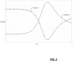
- FIG. 3 depicts a plot of the value of capacitor C b1 of bridge circuit 32 and the output current measured by respective sensors 22a, 22b.
- changing the value of capacitor C b1 causes the current (the respective values of the electrical parameter current in FIG. 3 ) through respective sensors 22a, 22b to correspondingly change.
- an increase in current passing though sensor 2 22b corresponds to a decrease in current through sensor 1 22a, and vice versa.
- the current through sensor 1 22a and sensor 2 22b is equal.
- varying C b1 enables varying the relationship between the current measured by respective sensor 1 22a and sensor 2 22b.
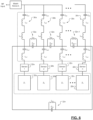
- FIG. 4 depicts a generalized view of splitter 16 for n branches or legs 30a, 30b, 30c, ..., 30n.
- FIG. 4 depicts matching network 14 receiving an RF input, such as from RF generator 12, and outputting a matched signal to splitter 16.
- Splitter 16 in FIG. 4 includes n branches which receive the signal output from match network 14 and splits the signal into a n signals output to respective sensors 1, 2, 3, ..., n (22a, 22b, 22c, ..., 22n).
- Sensors 1, 2, 3, ..., n (22a, 22b, 22c, ..., 22n) output RF signals to respective chambers 1, 2, 3, ..., n.
- each chamber is represented by a respective impedance Z 1 , Z 2 , Z 3 , ..., Z n (20a, 20b, 20c, ... , 20n).
- Splitter 16 of FIG. 4 shows n branches or legs 30a, 30b, 30c, ..., 30n interconnected by a respective balancing or bridge circuit 32a, 32b, ..., 30n-1.
- each leg or branch 30a, 30b, 30c, ..., 30n can be configured with resonant LC circuits as described above with respect to FIG. 2 .
- Splitter 16 also includes balancing or bridge circuits 32a, 32b, ..., 32n-1.
- Each bridge circuit 32 32a, 32b, ..., 32n-1 is configured as described above with respect to FIG. 2 .
- the output from splitter 16 legs or branches 30a, 30b, 30c, ..., 30n to respective impedances Z 1 , Z 2 , Z 3 , ..., Z n (20a, 20b, 20c, ... , 20n) can be varied to enable maintaining a predetermined relationship between a value of electrical parameter of each bridge or leg connected by a respective bridge circuit.
- each branch circuit can be controlled by controller 24 so that the power output by each leg or branch 30a, 30b, 30c, ..., 30n-1 of splitter 16 may be controlled dynamically.
- Each balancing or bridge circuit 32a, 32b, ... , 32n can be controlled as described above with respect to FIG. 2 to enable controlling electrical parameter values in each leg 30a, 30b, ... , 30n to predefined relationships. In various embodiments, a number of predefined relationships can be maintained between values of the electrical parameters of respective legs 30a, 30b, ... , 30n.
- changing the value of capacitors causes the current through respective sensors 22a, 22b, 22c, 22d to correspondingly change. Where the waveforms cross, the current through sensors corresponding to the crossing waveforms is equal.
- varying C b1 , C b2 , and C b3 enables varying the relationship between the currents measured by sensor 1 22a, sensor 2 22b, sensor 3 22c, and sensor 4 22d.
- FIG. 6 depicts a configuration similar to FIG. 4 , with the addition of a bridge circuit 32n.
- FIG. 6 operates similarly to FIG. 4 with bridge circuit 32n controlling voltage, current, power, impedance, frequency, or phase between branches 30a and 30n.
- changing the value of the capacitors causes the current (the respective values of the electrical parameter current in FIG. 7 ) through respective sensors 22a, 22b, 22c, 22d to correspondingly change. Where the waveforms cross, the current through the sensors is equal.
- varying C b1 , C b2 , C b3 , and C b4 enables varying the relationship between the currents measured by sensor 1 22a, sensor 2 22b, sensor 3 22c, and sensor 4 22d.
- An offset for systematic benefits can be subsequently added to the new load power set point.
- a is recomputed to account for dynamic effects in the plant.
- FIGS. 8 and 9 a Monte Carlo simulation for a dynamic power delivery system and plasma chambers demonstrates the efficacy of the subject disclosure.
- the cumulative density function for the initial root mean square (RMS) load power error is shown in FIG. 8 as variation from approximately 2.5% to 35%.
- the final distribution of RMS load power error in FIG. 9 does not exceed 1% and is approximately less than 0.1% RMS error 90% of the time.
- An alternative minimization approach is described below.
- the previous equations describe a cost function that minimizes the difference between an average load power and the load power corresponding to the active chambers.
- An alternative approach utilizes a cost function that minimizes the electrical parameter (such as load power) difference between the electrical parameter (such as load power) measurements corresponding to the active chambers.
- the power delivery system determines adjustments to an offset for systematic benefits can be subsequently added to the new load power set point.
- a is recomputed to account for dynamic effects in the plant.
- the matrix form that is used in both minimization methods has a row included as the last entry in the matrix.
- This is a constraint equation to force the a result to converge to an average load power P DA .
- this equation could be omitted or modified for other constraints.
- One possible permutation of the constraint equation could be non-uniform power level where the K -1 constant is replaced by weighted values with the requirement the weighted values sum to 1. This yields a predetermined relationship between the electrical parameter values which may be one or both non-uniform and not minimized.
- load power as an example of providing unified control.
- the concept is extendable for the purpose of unified control using a different electrical parameter or variable in lieu of the load power variable in the minimized cost function.
- These electrical parameter variables could include the measured voltage, current, impedance, frequency, power, or phase.
- Phase could include the phase difference between voltage and current, or the phase of the measured voltage or the measured current.
- Further extension may include functions of these variables.
- These functions could include plasma parameters that are derived from a set of these measured values. For instance, ion mass/flux and plasma density and electron temperature can be determined from the measurements of the common analysis module.
- ⁇ may take on an alternate definition in lieu of E [ ⁇ ].
- An offset for systematic benefits can be subsequently added to the new set point.
- a is recomputed to account for dynamic effects in the plant.
- FIGS. 10a-10c indicate various embodiments of balancing or bridge circuit 32.
- balancing circuit 32 is shown as a parallel LC circuit.
- FIG. 10a indicates an embodiment of balancing circuit 32 including a series LC circuit.
- FIG. 10b indicates a balancing circuit 32 implemented as a capacitor.
- FIG. 10c indicates a balancing circuit 32 implemented as an inductor.
- a distribution scheme to balance RF power to various node outputs include when manufacturing multiple targets on a single process tool that contains multiple plasma chambers, the work piece may be exposed to the same amount of power during a uniform processing time for all RF plasma chambers associated with the process tool.
- the system of the present disclosure allows load sharing between electrodes with a bridging circuit to keep power uniform between electrodes and impedance high for isolation.
- a single analysis module may be configured to analyze multiple RF sensors to achieve unified control across the entire tool can be accomplished.
- the bridge element is derived from a high impedance source through a parallel resonant circuit.
- One of the elements of the parallel circuit is variable to allow power tuning between electrodes.
- Unified control can be accomplished with the uniform delivered power to the active chambers on the tool. Dynamic utilization of the plasma processing tool may not simultaneously use all of the chambers. Because the common analysis module couples to the RF sensors, control can be arbitrated to only those RF plasma chambers that are active on the tool.
- the analysis module or controller can provide an actuating signal corresponding to the unified parameter, e.g. delivered power.
- the control signal can be communicated via a digital link, e.g. RS-232, or accomplished through a network scheme via Ethernet.
- the controller approach described herein is optimal to converge the distinct active plasma chambers to a minimum load power error
- Spatial and functional relationships between elements are described using various terms, including “connected,” “engaged,” “coupled,” “adjacent,” “next to,” “on top of,” “above,” “below,” and “disposed.” Unless explicitly described as being “direct,” when a relationship between first and second elements is described in the above disclosure, that relationship can be a direct relationship where no other intervening elements are present between the first and second elements, but can also be an indirect relationship where one or more intervening elements are present (either spatially or functionally) between the first and second elements.
- the phrase at least one of A, B, and C should be construed to mean a logical (A OR B OR C), using a non-exclusive logical OR, and should not be construed to mean "at least one of A, at least one of B, and at least one of C.”
- the direction of an arrow generally demonstrates the flow of information (such as data or instructions) that is of interest to the illustration.
- information such as data or instructions
- the arrow may point from element A to element B. This unidirectional arrow does not imply that no other information is transmitted from element B to element A.
- element B may send requests for, or receipt acknowledgements of, the information to element A.
- module or the term “controller” may be replaced with the term “circuit.”
- the term “module” may refer to, be part of, or include: an Application Specific Integrated Circuit (ASIC); a digital, analog, or mixed analog/digital discrete circuit; a digital, analog, or mixed analog/digital integrated circuit; a combinational logic circuit; a field programmable gate array (FPGA); a processor circuit (shared, dedicated, or group) that executes code; a memory circuit (shared, dedicated, or group) that stores code executed by the processor circuit; other suitable hardware components that provide the described functionality; or a combination of some or all of the above, such as in a system-on-chip.
- ASIC Application Specific Integrated Circuit
- FPGA field programmable gate array
- the module may include one or more interface circuits.
- the interface circuits may include wired or wireless interfaces that are connected to a local area network (LAN), the Internet, a wide area network (WAN), or combinations thereof.
- LAN local area network
- WAN wide area network
- the functionality of any given module of the present disclosure may be distributed among multiple modules that are connected via interface circuits. For example, multiple modules may allow load balancing.
- a server (also known as remote, or cloud) module may accomplish some functionality on behalf of a client module.
- Some or all hardware features of a module may be defined using a language for hardware description, such as IEEE Standard 1364-2005 (commonly called “Verilog”) and IEEE Standard 1076-2008 (commonly called “VHDL”).
- the hardware description language may be used to manufacture and/or program a hardware circuit.
- some or all features of a module may be defined by a language, such as IEEE 1666-2005 (commonly called “SystemC”), that encompasses both code, as described below, and hardware description.
- code may include software, firmware, and/or microcode, and may refer to programs, routines, functions, classes, data structures, and/or objects.
- shared processor circuit encompasses a single processor circuit that executes some or all code from multiple modules.
- group processor circuit encompasses a processor circuit that, in combination with additional processor circuits, executes some or all code from one or more modules. References to multiple processor circuits encompass multiple processor circuits on discrete dies, multiple processor circuits on a single die, multiple cores of a single processor circuit, multiple threads of a single processor circuit, or a combination of the above.
- shared memory circuit encompasses a single memory circuit that stores some or all code from multiple modules.
- group memory circuit encompasses a memory circuit that, in combination with additional memories, stores some or all code from one or more modules.
- the term memory circuit is a subset of the term computer-readable medium.
- the term computer-readable medium does not encompass transitory electrical or electromagnetic signals propagating through a medium (such as on a carrier wave); the term computer-readable medium may therefore be considered tangible and non-transitory.
- Non-limiting examples of a non-transitory computer-readable medium are nonvolatile memory circuits (such as a flash memory circuit, an erasable programmable read-only memory circuit, or a mask read-only memory circuit), volatile memory circuits (such as a static random access memory circuit or a dynamic random access memory circuit), magnetic storage media (such as an analog or digital magnetic tape or a hard disk drive), and optical storage media (such as a CD, a DVD, or a Blu-ray Disc).
- nonvolatile memory circuits such as a flash memory circuit, an erasable programmable read-only memory circuit, or a mask read-only memory circuit
- volatile memory circuits such as a static random access memory circuit or a dynamic random access memory circuit
- magnetic storage media such as an analog or digital magnetic tape or a hard disk drive
- optical storage media such as a CD, a DVD, or a Blu-ray Disc
- the apparatuses and methods described in this application may be partially or fully implemented by a special purpose computer created by configuring a general purpose computer to execute one or more particular functions embodied in computer programs.
- the functional blocks and flowchart elements described above serve as software specifications, which can be translated into the computer programs by the routine work of a skilled technician or programmer.
- the computer programs include processor-executable instructions that are stored on at least one non-transitory computer-readable medium.
- the computer programs may also include or rely on stored data.
- the computer programs may encompass a basic input/output system (BIOS) that interacts with hardware of the special purpose computer, device drivers that interact with particular devices of the special purpose computer, one or more operating systems, user applications, background services, background applications, etc.
- BIOS basic input/output system
- the computer programs may include: (i) descriptive text to be parsed, such as HTML (hypertext markup language), XML (extensible markup language), or JSON (JavaScript Object Notation), (ii) assembly code, (iii) object code generated from source code by a compiler, (iv) source code for execution by an interpreter, (v) source code for compilation and execution by a just-in-time compiler, etc.
- source code may be written using syntax from languages including C, C++, C#, Objective-C, Swift, Haskell, Go, SQL, R, Lisp, Java ® , Fortran, Perl, Pascal, Curl, OCaml, Javascript ® , HTML5 (Hypertext Markup Language 5th revision), Ada, ASP (Active Server Pages), PHP (PHP: Hypertext Preprocessor), Scala, Eiffel, Smalltalk, Erlang, Ruby, FlashO, Visual Basic ® , Lua, MATLAB, SIMULINK, and Python ® .
Landscapes
- Physics & Mathematics (AREA)
- Engineering & Computer Science (AREA)
- Plasma & Fusion (AREA)
- Chemical & Material Sciences (AREA)
- Analytical Chemistry (AREA)
- Plasma Technology (AREA)
Claims (15)
- Elektrischer Splitter (16), konfiguriert zum Empfangen eines HF-Ausgangssignals und zum Erzeugen eines ersten HF-Ausgangs und eines zweiten HF-Ausgangs für eine erste Last (20a) bzw. eine zweite Last (20b), der Folgendes umfasst:einen ersten Zweig (30a), der zum Übertragen des ersten HF-Ausgangs zur ersten Last konfiguriert ist;einen zweiten Zweig (30b), der zum Übertragen des zweiten HF-Ausgangs zur zweiten Last konfiguriert ist; undeine Ausgleichsschaltung (32), die zwischen den ersten Zweig (30a) und den zweiten Zweig (30b) geschaltet ist, wobei die Ausgleichsschaltung (32) zum Steuern eines ersten Wertes eines mit dem ersten Zweig (30a) oder dem zweiten Zweig (30b) assoziierten elektrischen Parameters und eines zweiten Wertes des mit einem anderen von erstem Zweig (30a) und zweitem Zweig (30b) assoziierten elektrischen Parameters konfiguriert ist,wobei der erste Wert und der zweite Wert in einem vordefinierten Verhältnis steuerbar sind.
- Elektrischer Splitter (16) nach Anspruch 1, wobei der elektrische Parameter einer von Spannung, Strom, Leistung, Impedanz, Frequenz und Phase ist.
- Elektrischer Splitter (16) nach Anspruch 1 oder 2, wobei die Ausgleichsschaltung (32) zwischen dem ersten Zweig (30a) und dem zweiten Zweig (30b) nebengeschlossen ist und ferner einen Induktor (Lb1) und/oder einen Kondensator (Cb1) umfasst.
- Elektrischer Splitter (16) nach Anspruch 3, wobei der Induktor (Lb1) und der Kondensator (Cb1) parallel geschaltet sind.
- Elektrischer Splitter (16) nach Anspruch 4, wobei der Kondensator (Cb1) und/oder der Induktor (Lb1) variabel und steuerbar ist/sind, um das Verhältnis zwischen dem ersten Wert und dem zweiten Wert zu variieren.
- Elektrischer Splitter (16) nach Anspruch 5, der ferner eine Steuerung (24) umfasst, die zum Variieren des Kondensators (Cb1) und/oder des Induktors (Lb1) konfiguriert ist, um das Verhältnis zwischen dem ersten Wert und dem zweiten Wert zu variieren.
- Elektrischer Splitter (16) nach einem vorherigen Anspruch, wobei die Ausgleichsschaltung mindestens eine Komponente enthält, die variabel ist, um das Verhältnis zwischen dem ersten Wert und dem zweiten Wert zu justieren.
- Elektrischer Splitter (16) nach einem vorherigen Anspruch, der ferner einen oder mehrere weitere Zweige (30c) umfasst, die jeweils zum Übertragen eines HF-Ausgangs zu einer weiteren Last (20c) konfiguriert sind, wobei das vordefinierte Verhältnis gemäß dem Minimieren einer Differenz zwischen dem ersten Wert und dem zweiten Wert bestimmt wird gemäß einem von:

 i und j sich auf einen der K Zweige (30a, 30b, ..., 30n) des elektrischen Splitters (16) beziehen;(der elektrische Parameter ist;α n ein Koeffizient entsprechend einem n-ten Zweig ist; undχ n ein erfasster Wert des elektrischen Parameters entsprechend einem n-ten Zweig ist.
 - Elektrischer Splitter nach Anspruch 8, wobei ein Sollwert für den elektrischen Parameter für einen j-ten Zweig bestimmt wird gemäß:
 αj der Koeffizient entsprechend dem j-ten Zweig ist, undχj (n) ein erfasster Wert des elektrischen Parameters entsprechend dem j-ten Zweig während einer n-ten Iteration für einen aktuellen Sollwert ist.
 - Elektrischer Splitter nach einem vorherigen Anspruch, wobei der erste Zweig (30a) und/oder der zweite Zweig (30b) eine Isolationsschaltung (Ca1'/La1'; Ca2'/La2') beinhaltet/-n, um den ersten Zweig (30a) und/oder den zweiten Zweig (30b) von dem anderen aus erstem Zweig (30a) und zweitem Zweig (30b) zu isolieren, und die Isolationsschaltung einen Induktor (La1', La2') und/oder einen Kondensator (Ca1', Ca2') beinhaltet.
- Elektrischer Splitter (16) nach einem vorherigen Anspruch, wobei der elektrische Splitter (16) zum Erzeugen eines dritten HF-Ausgangs für eine dritte Last (20c) konfiguriert ist und ferner Folgendes umfasst:einen dritten Zweig (30c), der zum Übertragen des dritten HF-Ausgangs zur dritten Last (20c) konfiguriert ist; undeine zweite Ausgleichsschaltung (32b), die zwischen einen ausgewählten aus erstem Zweig (30a) und zweitem Zweig (30b) und drittem Zweig (30c) geschaltet ist,wobei die zweite Ausgleichsschaltung (32b) zum Variieren eines dritten Wertes des elektrischen Parameters und des ersten Wertes oder des zweiten Wertes entsprechend dem ausgewählten aus erstem Zweig (30a) und zweitem Zweig (30b) konfiguriert ist, undwobei der dritte Wert und der erste Wert oder der zweite Wert entsprechend dem ausgewählten aus erstem Zweig (30a) und zweitem Zweig (30b) in einem zweiten vordefinierten Verhältnis steuerbar sind.
- Elektrischer Splitter (16) nach Anspruch 11, der ferner Folgendes umfasst:eine dritte Ausgleichsschaltung (32n), die zwischen dem anderen aus dem ausgewählten ersten Zweig (30a) und zweiten Zweig (30b) und dritten Zweig (30c) geschaltet ist,wobei die dritte Ausgleichsschaltung (32n) zum Variieren des dritten Wertes und eines anderen aus erstem Wert und zweitem Wert entsprechend dem anderen aus erstem Zweig (30a) und zweitem Zweig (30b) konfiguriert ist, undwobei der dritte Wert und der andere aus erstem Wert und zweitem Wert entsprechend dem anderen aus ausgewähltem erstem Zweig (30a) und zweitem Zweig (30b) auf ein drittes vordefiniertes Verhältnis steuerbar sind.
- Elektrischer Splitter (16) nach Anspruch 12, wobei der erste, der zweite und der dritte Wert auf gleiche oder unterschiedliche vordefinierte Verhältnisse steuerbar sind.
- RF-System (10) mit dem elektrischen Splitter nach einem der vorherigen Ansprüche, das ferner Folgendes umfasst:eine HF-Leistungsquelle (12), die ein HF-Signal erzeugt;
undeine Steuerung (24), die zum Variieren der mindestens einen Komponente konfiguriert ist,wobei die Steuerung (24) zum Steuern der mindestens einen Komponente konfiguriert ist, so dass der erste Wert und der zweite Wert auf ein vordefiniertes Verhältnis gesteuert werden. - Elektrischer Splitter nach einem der Ansprüche 1-5 oder 7-13, der ferner eine Steuerung (24) umfasst, die zum Variieren des Verhältnisses gemäß Erfassungssignalen konfiguriert ist, die gemäß mit dem ersten Wert bzw. dem zweiten Wert variieren.
Applications Claiming Priority (3)
| Application Number | Priority Date | Filing Date | Title |
|---|---|---|---|
| US201762551637P | 2017-08-29 | 2017-08-29 | |
| US16/112,055 US10536130B2 (en) | 2017-08-29 | 2018-08-24 | Balancing RF circuit and control for a cross-coupled SIMO distribution network |
| PCT/US2018/048351 WO2019046305A1 (en) | 2017-08-29 | 2018-08-28 | RF CIRCUIT FOR BALANCING, AND CONTROL OF A SIMO CROSS-COUPLING DISTRIBUTION NETWORK |
Publications (3)
| Publication Number | Publication Date |
|---|---|
| EP3676864A1 EP3676864A1 (de) | 2020-07-08 |
| EP3676864A4 EP3676864A4 (de) | 2021-08-04 |
| EP3676864B1 true EP3676864B1 (de) | 2023-08-09 |
Family
ID=65435644
Family Applications (1)
| Application Number | Title | Priority Date | Filing Date |
|---|---|---|---|
| EP18849592.3A Active EP3676864B1 (de) | 2017-08-29 | 2018-08-28 | Hf-kompensationsschaltung und steuerung für ein kreuzgekoppeltes simo-verteilnetz |
Country Status (8)
| Country | Link |
|---|---|
| US (1) | US10536130B2 (de) |
| EP (1) | EP3676864B1 (de) |
| JP (1) | JP7013567B2 (de) |
| KR (1) | KR102360431B1 (de) |
| CN (1) | CN111033681B (de) |
| SG (1) | SG11201912726RA (de) |
| TW (1) | TWI673953B (de) |
| WO (1) | WO2019046305A1 (de) |
Families Citing this family (12)
| Publication number | Priority date | Publication date | Assignee | Title |
|---|---|---|---|---|
| KR102791775B1 (ko) | 2019-05-07 | 2025-04-03 | 램 리써치 코포레이션 | 폐루프 다중 출력 rf 매칭 |
| CN118866641A (zh) | 2019-07-31 | 2024-10-29 | 朗姆研究公司 | 具有多个输出端口的射频功率产生器 |
| KR20220088474A (ko) * | 2019-10-25 | 2022-06-27 | 램 리써치 코포레이션 | 멀티 스테이션 집적 회로 제조 챔버에서 rf (radio frequency) 전력 임밸런싱 (imbalancing) |
| KR102896979B1 (ko) * | 2019-11-15 | 2025-12-05 | 램 리써치 코포레이션 | 튜닝 회로들에서 주파수 기반 임피던스 조정 |
| WO2021113387A1 (en) | 2019-12-02 | 2021-06-10 | Lam Research Corporation | Impedance transformation in radio-frequency-assisted plasma generation |
| CN112992636B (zh) * | 2019-12-17 | 2023-09-29 | 中微半导体设备(上海)股份有限公司 | 用于等离子体处理设备的射频功率源装置和射频功率分配方法 |
| US11994542B2 (en) | 2020-03-27 | 2024-05-28 | Lam Research Corporation | RF signal parameter measurement in an integrated circuit fabrication chamber |
| KR20230021739A (ko) | 2020-06-12 | 2023-02-14 | 램 리써치 코포레이션 | Rf 커플링 구조체들에 의한 플라즈마 형성의 제어 |
| DE102022111529A1 (de) * | 2022-05-09 | 2023-11-09 | TRUMPF Hüttinger GmbH + Co. KG | Stromversorgungsanordnung, Plasmaerzeugungseinrichtung und Verfahren zur Steuerung mehrerer Plasmaprozesse |
| CN117353260B (zh) * | 2023-11-02 | 2024-08-06 | 深圳市恒运昌真空技术股份有限公司 | 一种基于平衡功放的能量过冲抑制电路及其控制方法 |
| CN120261246A (zh) * | 2024-01-02 | 2025-07-04 | 北京北方华创微电子装备有限公司 | 射频功率输出电路和半导体工艺设备 |
| US20250285840A1 (en) * | 2024-03-05 | 2025-09-11 | Applied Materials, Inc. | Rf power splitting and control |
Family Cites Families (38)
| Publication number | Priority date | Publication date | Assignee | Title |
|---|---|---|---|---|
| US5175472A (en) | 1991-12-30 | 1992-12-29 | Comdel, Inc. | Power monitor of RF plasma |
| JPH07322510A (ja) * | 1994-05-30 | 1995-12-08 | Nec Eng Ltd | アンバランス吸収抵抗冷却回路 |
| AU2003195A (en) | 1994-06-21 | 1996-01-04 | Boc Group, Inc., The | Improved power distribution for multiple electrode plasma systems using quarter wavelength transmission lines |
| US6046594A (en) | 1997-02-11 | 2000-04-04 | Advanced Energy Voorhees, Inc. | Method and apparatus for monitoring parameters of an RF powered load in the presence of harmonics |
| US6351683B1 (en) | 1997-09-17 | 2002-02-26 | Tokyo Electron Limited | System and method for monitoring and controlling gas plasma processes |
| US6199506B1 (en) | 1999-06-30 | 2001-03-13 | Novellus Systems, Inc. | Radio frequency supply circuit for in situ cleaning of plasma-enhanced chemical vapor deposition chamber using NF3 or NF3/He mixture |
| JP2001032077A (ja) | 1999-07-19 | 2001-02-06 | Mitsubishi Heavy Ind Ltd | プラズマcvd製膜方法 |
| US6326584B1 (en) | 1999-12-31 | 2001-12-04 | Litmas, Inc. | Methods and apparatus for RF power delivery |
| JP5165825B2 (ja) | 2000-01-10 | 2013-03-21 | 東京エレクトロン株式会社 | 分割された電極集合体並びにプラズマ処理方法。 |
| AU2001223384A1 (en) | 2000-02-23 | 2001-09-03 | Unaxis Balzers Aktiengesellschaft | Method for controlling plasma density or the distribution thereof |
| JP3966669B2 (ja) | 2000-03-24 | 2007-08-29 | 株式会社日立国際電気 | プラズマ処理装置 |
| WO2001073814A2 (en) | 2000-03-28 | 2001-10-04 | Tokyo Electron Limited | Method and apparatus for controlling power delivered to a multiple segment electrode |
| AU2001251216A1 (en) | 2000-03-30 | 2001-10-15 | Tokyo Electron Limited | Optical monitoring and control system and method for plasma reactors |
| US6583572B2 (en) | 2001-03-30 | 2003-06-24 | Lam Research Corporation | Inductive plasma processor including current sensor for plasma excitation coil |
| US6677711B2 (en) | 2001-06-07 | 2004-01-13 | Lam Research Corporation | Plasma processor method and apparatus |
| JP3980314B2 (ja) | 2001-10-01 | 2007-09-26 | シャープ株式会社 | プラズマ処理装置およびプラズマ処理方法 |
| US6998349B2 (en) | 2003-02-06 | 2006-02-14 | Lam Research Corporation | System, method and apparatus for automatic control of an RF generator for maximum efficiency |
| US7452824B2 (en) | 2003-05-16 | 2008-11-18 | Applied Materials, Inc. | Method of characterizing a chamber based upon concurrent behavior of selected plasma parameters as a function of plural chamber parameters |
| US7042311B1 (en) | 2003-10-10 | 2006-05-09 | Novellus Systems, Inc. | RF delivery configuration in a plasma processing system |
| JP4551081B2 (ja) | 2003-11-12 | 2010-09-22 | 三菱重工業株式会社 | プラズマcvd装置の給電システム及び給電方法 |
| CN100550273C (zh) * | 2003-12-18 | 2009-10-14 | 应用材料公司 | 双频rf匹配 |
| JP2005347205A (ja) | 2004-06-07 | 2005-12-15 | Toray Ind Inc | 常圧放電処理用電源装置、および常圧放電処理装置 |
| US7323116B2 (en) | 2004-09-27 | 2008-01-29 | Lam Research Corporation | Methods and apparatus for monitoring a process in a plasma processing system by measuring self-bias voltage |
| CN101057310B (zh) | 2004-11-12 | 2010-11-03 | 欧瑞康太阳Ip股份公司(特吕巴赫) | 适于大面积衬底的电容性耦合rf等离子体反应器的阻抗匹配 |
| US7602127B2 (en) | 2005-04-18 | 2009-10-13 | Mks Instruments, Inc. | Phase and frequency control of a radio frequency generator from an external source |
| US7286948B1 (en) | 2006-06-16 | 2007-10-23 | Applied Materials, Inc. | Method for determining plasma characteristics |
| US8438990B2 (en) * | 2008-09-30 | 2013-05-14 | Applied Materials, Inc. | Multi-electrode PECVD source |
| US8282983B1 (en) | 2008-09-30 | 2012-10-09 | Novellus Systems, Inc. | Closed loop control system for RF power balancing of the stations in a multi-station processing tool with shared RF source |
| US20100295472A1 (en) | 2009-05-06 | 2010-11-25 | Polar Semiconductor, Inc. | Power supply for floating loads |
| US8875657B2 (en) | 2010-01-26 | 2014-11-04 | Applied Materials, Inc. | Balancing RF bridge assembly |
| US20130337657A1 (en) | 2012-06-19 | 2013-12-19 | Plasmasi, Inc. | Apparatus and method for forming thin protective and optical layers on substrates |
| JP2014089876A (ja) | 2012-10-30 | 2014-05-15 | Tokyo Electron Ltd | プラズマ処理装置 |
| US9336995B2 (en) | 2013-04-26 | 2016-05-10 | Mks Instruments, Inc. | Multiple radio frequency power supply control of frequency and phase |
| US9263350B2 (en) * | 2014-06-03 | 2016-02-16 | Lam Research Corporation | Multi-station plasma reactor with RF balancing |
| KR101704116B1 (ko) * | 2014-07-08 | 2017-02-07 | 엘지이노텍 주식회사 | 컨버터 |
| US9704692B2 (en) | 2015-07-01 | 2017-07-11 | Lam Research Corporation | System for instantaneous radiofrequency power measurement and associated methods |
| US9721758B2 (en) | 2015-07-13 | 2017-08-01 | Mks Instruments, Inc. | Unified RF power delivery single input, multiple output control for continuous and pulse mode operation |
| KR101777762B1 (ko) | 2015-09-03 | 2017-09-12 | 에이피시스템 주식회사 | 고주파 전원 공급장치 및 이를 포함하는 기판 처리장치 |
-
2018
- 2018-08-24 US US16/112,055 patent/US10536130B2/en active Active
- 2018-08-28 JP JP2020512416A patent/JP7013567B2/ja active Active
- 2018-08-28 EP EP18849592.3A patent/EP3676864B1/de active Active
- 2018-08-28 WO PCT/US2018/048351 patent/WO2019046305A1/en not_active Ceased
- 2018-08-28 CN CN201880054854.4A patent/CN111033681B/zh not_active Expired - Fee Related
- 2018-08-28 KR KR1020207008964A patent/KR102360431B1/ko active Active
- 2018-08-28 SG SG11201912726RA patent/SG11201912726RA/en unknown
- 2018-08-29 TW TW107130163A patent/TWI673953B/zh active
Also Published As
| Publication number | Publication date |
|---|---|
| CN111033681A (zh) | 2020-04-17 |
| KR102360431B1 (ko) | 2022-02-14 |
| WO2019046305A1 (en) | 2019-03-07 |
| CN111033681B (zh) | 2023-03-10 |
| JP7013567B2 (ja) | 2022-01-31 |
| EP3676864A4 (de) | 2021-08-04 |
| US10536130B2 (en) | 2020-01-14 |
| EP3676864A1 (de) | 2020-07-08 |
| US20190068158A1 (en) | 2019-02-28 |
| TW202019088A (zh) | 2020-05-16 |
| JP2020532826A (ja) | 2020-11-12 |
| SG11201912726RA (en) | 2020-01-30 |
| TWI673953B (zh) | 2019-10-01 |
| KR20200037430A (ko) | 2020-04-08 |
Similar Documents
| Publication | Publication Date | Title |
|---|---|---|
| EP3676864B1 (de) | Hf-kompensationsschaltung und steuerung für ein kreuzgekoppeltes simo-verteilnetz | |
| EP3631836B1 (de) | Stückweise hf-leistungssysteme und verfahren zur einspeisung von vorverzerten hf-vorspannungssignalen in eine elektrode einer verarbeitungskammer | |
| US10304669B1 (en) | Adaptive counter measure control thwarting IMD jamming impairments for RF plasma systems | |
| US11536755B2 (en) | System and method for arc detection using a bias RF generator signal | |
| CN108140530B (zh) | 等离子rf偏置消除系统 | |
| US11527384B2 (en) | Apparatus and tuning method for mitigating RF load impedance variations due to periodic disturbances | |
| CN112313876A (zh) | 基于校正方案和性能重复性的阻抗匹配网络模型 | |
| WO2023018448A1 (en) | Adaptive pulse shaping with post match sensor | |
| US12087549B2 (en) | Demagnetizing coils for linearity improvement of current ratio of plasma processing systems | |
| EP4416754A1 (de) | Impedanzanpassung in einem hf-stromerzeugungssystem | |
| WO2024158548A1 (en) | Non-invasive ied estimation for pulsed-dc and low frequency applications | |
| TWI881363B (zh) | 用於配備有離子能量感測器的多電極系統的電漿工藝控制的rf發生器、rf系統和電腦可讀介質 | |
| US20260043884A1 (en) | High Accuracy Detector For Non-Sinusoidal Generator | |
| WO2026096271A1 (en) | System and method for reducing intermodulation distortion in a plasma chamber |
Legal Events
| Date | Code | Title | Description |
|---|---|---|---|
| STAA | Information on the status of an ep patent application or granted ep patent |
Free format text: STATUS: THE INTERNATIONAL PUBLICATION HAS BEEN MADE |
|
| PUAI | Public reference made under article 153(3) epc to a published international application that has entered the european phase |
Free format text: ORIGINAL CODE: 0009012 |
|
| STAA | Information on the status of an ep patent application or granted ep patent |
Free format text: STATUS: REQUEST FOR EXAMINATION WAS MADE |
|
| 17P | Request for examination filed |
Effective date: 20200131 |
|
| AK | Designated contracting states |
Kind code of ref document: A1 Designated state(s): AL AT BE BG CH CY CZ DE DK EE ES FI FR GB GR HR HU IE IS IT LI LT LU LV MC MK MT NL NO PL PT RO RS SE SI SK SM TR |
|
| AX | Request for extension of the european patent |
Extension state: BA ME |
|
| RIN1 | Information on inventor provided before grant (corrected) |
Inventor name: JANG, JEONGSEOK Inventor name: HUH, JIN Inventor name: COUMOU, DAVID, J. Inventor name: BROWN, DENNIS, M. |
|
| DAV | Request for validation of the european patent (deleted) | ||
| DAX | Request for extension of the european patent (deleted) | ||
| A4 | Supplementary search report drawn up and despatched |
Effective date: 20210706 |
|
| RIC1 | Information provided on ipc code assigned before grant |
Ipc: H01J 37/32 20060101AFI20210630BHEP Ipc: H03H 7/48 20060101ALI20210630BHEP |
|
| GRAP | Despatch of communication of intention to grant a patent |
Free format text: ORIGINAL CODE: EPIDOSNIGR1 |
|
| STAA | Information on the status of an ep patent application or granted ep patent |
Free format text: STATUS: GRANT OF PATENT IS INTENDED |
|
| RIC1 | Information provided on ipc code assigned before grant |
Ipc: H03H 7/48 20060101ALI20230131BHEP Ipc: H01J 37/32 20060101AFI20230131BHEP |
|
| INTG | Intention to grant announced |
Effective date: 20230228 |
|
| GRAS | Grant fee paid |
Free format text: ORIGINAL CODE: EPIDOSNIGR3 |
|
| GRAA | (expected) grant |
Free format text: ORIGINAL CODE: 0009210 |
|
| STAA | Information on the status of an ep patent application or granted ep patent |
Free format text: STATUS: THE PATENT HAS BEEN GRANTED |
|
| AK | Designated contracting states |
Kind code of ref document: B1 Designated state(s): AL AT BE BG CH CY CZ DE DK EE ES FI FR GB GR HR HU IE IS IT LI LT LU LV MC MK MT NL NO PL PT RO RS SE SI SK SM TR |
|
| REG | Reference to a national code |
Ref country code: GB Ref legal event code: FG4D |
|
| REG | Reference to a national code |
Ref country code: CH Ref legal event code: EP |
|
| REG | Reference to a national code |
Ref country code: DE Ref legal event code: R096 Ref document number: 602018055179 Country of ref document: DE |
|
| REG | Reference to a national code |
Ref country code: IE Ref legal event code: FG4D |
|
| REG | Reference to a national code |
Ref country code: LT Ref legal event code: MG9D |
|
| REG | Reference to a national code |
Ref country code: NL Ref legal event code: MP Effective date: 20230809 |
|
| REG | Reference to a national code |
Ref country code: AT Ref legal event code: MK05 Ref document number: 1598517 Country of ref document: AT Kind code of ref document: T Effective date: 20230809 |
|
| PG25 | Lapsed in a contracting state [announced via postgrant information from national office to epo] |
Ref country code: GR Free format text: LAPSE BECAUSE OF FAILURE TO SUBMIT A TRANSLATION OF THE DESCRIPTION OR TO PAY THE FEE WITHIN THE PRESCRIBED TIME-LIMIT Effective date: 20231110 |
|
| PG25 | Lapsed in a contracting state [announced via postgrant information from national office to epo] |
Ref country code: IS Free format text: LAPSE BECAUSE OF FAILURE TO SUBMIT A TRANSLATION OF THE DESCRIPTION OR TO PAY THE FEE WITHIN THE PRESCRIBED TIME-LIMIT Effective date: 20231209 |
|
| PG25 | Lapsed in a contracting state [announced via postgrant information from national office to epo] |
Ref country code: SE Free format text: LAPSE BECAUSE OF FAILURE TO SUBMIT A TRANSLATION OF THE DESCRIPTION OR TO PAY THE FEE WITHIN THE PRESCRIBED TIME-LIMIT Effective date: 20230809 Ref country code: RS Free format text: LAPSE BECAUSE OF FAILURE TO SUBMIT A TRANSLATION OF THE DESCRIPTION OR TO PAY THE FEE WITHIN THE PRESCRIBED TIME-LIMIT Effective date: 20230809 Ref country code: PT Free format text: LAPSE BECAUSE OF FAILURE TO SUBMIT A TRANSLATION OF THE DESCRIPTION OR TO PAY THE FEE WITHIN THE PRESCRIBED TIME-LIMIT Effective date: 20231211 Ref country code: NO Free format text: LAPSE BECAUSE OF FAILURE TO SUBMIT A TRANSLATION OF THE DESCRIPTION OR TO PAY THE FEE WITHIN THE PRESCRIBED TIME-LIMIT Effective date: 20231109 Ref country code: NL Free format text: LAPSE BECAUSE OF FAILURE TO SUBMIT A TRANSLATION OF THE DESCRIPTION OR TO PAY THE FEE WITHIN THE PRESCRIBED TIME-LIMIT Effective date: 20230809 Ref country code: LV Free format text: LAPSE BECAUSE OF FAILURE TO SUBMIT A TRANSLATION OF THE DESCRIPTION OR TO PAY THE FEE WITHIN THE PRESCRIBED TIME-LIMIT Effective date: 20230809 Ref country code: LT Free format text: LAPSE BECAUSE OF FAILURE TO SUBMIT A TRANSLATION OF THE DESCRIPTION OR TO PAY THE FEE WITHIN THE PRESCRIBED TIME-LIMIT Effective date: 20230809 Ref country code: IS Free format text: LAPSE BECAUSE OF FAILURE TO SUBMIT A TRANSLATION OF THE DESCRIPTION OR TO PAY THE FEE WITHIN THE PRESCRIBED TIME-LIMIT Effective date: 20231209 Ref country code: HR Free format text: LAPSE BECAUSE OF FAILURE TO SUBMIT A TRANSLATION OF THE DESCRIPTION OR TO PAY THE FEE WITHIN THE PRESCRIBED TIME-LIMIT Effective date: 20230809 Ref country code: GR Free format text: LAPSE BECAUSE OF FAILURE TO SUBMIT A TRANSLATION OF THE DESCRIPTION OR TO PAY THE FEE WITHIN THE PRESCRIBED TIME-LIMIT Effective date: 20231110 Ref country code: FI Free format text: LAPSE BECAUSE OF FAILURE TO SUBMIT A TRANSLATION OF THE DESCRIPTION OR TO PAY THE FEE WITHIN THE PRESCRIBED TIME-LIMIT Effective date: 20230809 Ref country code: AT Free format text: LAPSE BECAUSE OF FAILURE TO SUBMIT A TRANSLATION OF THE DESCRIPTION OR TO PAY THE FEE WITHIN THE PRESCRIBED TIME-LIMIT Effective date: 20230809 |
|
| PG25 | Lapsed in a contracting state [announced via postgrant information from national office to epo] |
Ref country code: PL Free format text: LAPSE BECAUSE OF FAILURE TO SUBMIT A TRANSLATION OF THE DESCRIPTION OR TO PAY THE FEE WITHIN THE PRESCRIBED TIME-LIMIT Effective date: 20230809 |
|
| REG | Reference to a national code |
Ref country code: CH Ref legal event code: PL |
|
| PG25 | Lapsed in a contracting state [announced via postgrant information from national office to epo] |
Ref country code: LU Free format text: LAPSE BECAUSE OF NON-PAYMENT OF DUE FEES Effective date: 20230828 |
|
| PG25 | Lapsed in a contracting state [announced via postgrant information from national office to epo] |
Ref country code: ES Free format text: LAPSE BECAUSE OF FAILURE TO SUBMIT A TRANSLATION OF THE DESCRIPTION OR TO PAY THE FEE WITHIN THE PRESCRIBED TIME-LIMIT Effective date: 20230809 |
|
| PG25 | Lapsed in a contracting state [announced via postgrant information from national office to epo] |
Ref country code: SM Free format text: LAPSE BECAUSE OF FAILURE TO SUBMIT A TRANSLATION OF THE DESCRIPTION OR TO PAY THE FEE WITHIN THE PRESCRIBED TIME-LIMIT Effective date: 20230809 Ref country code: RO Free format text: LAPSE BECAUSE OF FAILURE TO SUBMIT A TRANSLATION OF THE DESCRIPTION OR TO PAY THE FEE WITHIN THE PRESCRIBED TIME-LIMIT Effective date: 20230809 Ref country code: LU Free format text: LAPSE BECAUSE OF NON-PAYMENT OF DUE FEES Effective date: 20230828 Ref country code: ES Free format text: LAPSE BECAUSE OF FAILURE TO SUBMIT A TRANSLATION OF THE DESCRIPTION OR TO PAY THE FEE WITHIN THE PRESCRIBED TIME-LIMIT Effective date: 20230809 Ref country code: EE Free format text: LAPSE BECAUSE OF FAILURE TO SUBMIT A TRANSLATION OF THE DESCRIPTION OR TO PAY THE FEE WITHIN THE PRESCRIBED TIME-LIMIT Effective date: 20230809 Ref country code: DK Free format text: LAPSE BECAUSE OF FAILURE TO SUBMIT A TRANSLATION OF THE DESCRIPTION OR TO PAY THE FEE WITHIN THE PRESCRIBED TIME-LIMIT Effective date: 20230809 Ref country code: CZ Free format text: LAPSE BECAUSE OF FAILURE TO SUBMIT A TRANSLATION OF THE DESCRIPTION OR TO PAY THE FEE WITHIN THE PRESCRIBED TIME-LIMIT Effective date: 20230809 Ref country code: SK Free format text: LAPSE BECAUSE OF FAILURE TO SUBMIT A TRANSLATION OF THE DESCRIPTION OR TO PAY THE FEE WITHIN THE PRESCRIBED TIME-LIMIT Effective date: 20230809 Ref country code: CH Free format text: LAPSE BECAUSE OF NON-PAYMENT OF DUE FEES Effective date: 20230831 |
|
| REG | Reference to a national code |
Ref country code: BE Ref legal event code: MM Effective date: 20230831 |
|
| REG | Reference to a national code |
Ref country code: DE Ref legal event code: R097 Ref document number: 602018055179 Country of ref document: DE |
|
| REG | Reference to a national code |
Ref country code: IE Ref legal event code: MM4A |
|
| PG25 | Lapsed in a contracting state [announced via postgrant information from national office to epo] |
Ref country code: MC Free format text: LAPSE BECAUSE OF FAILURE TO SUBMIT A TRANSLATION OF THE DESCRIPTION OR TO PAY THE FEE WITHIN THE PRESCRIBED TIME-LIMIT Effective date: 20230809 Ref country code: IT Free format text: LAPSE BECAUSE OF FAILURE TO SUBMIT A TRANSLATION OF THE DESCRIPTION OR TO PAY THE FEE WITHIN THE PRESCRIBED TIME-LIMIT Effective date: 20230809 |
|
| PLBE | No opposition filed within time limit |
Free format text: ORIGINAL CODE: 0009261 |
|
| STAA | Information on the status of an ep patent application or granted ep patent |
Free format text: STATUS: NO OPPOSITION FILED WITHIN TIME LIMIT |
|
| PG25 | Lapsed in a contracting state [announced via postgrant information from national office to epo] |
Ref country code: IE Free format text: LAPSE BECAUSE OF NON-PAYMENT OF DUE FEES Effective date: 20230828 |
|
| 26N | No opposition filed |
Effective date: 20240513 |
|
| PG25 | Lapsed in a contracting state [announced via postgrant information from national office to epo] |
Ref country code: IE Free format text: LAPSE BECAUSE OF NON-PAYMENT OF DUE FEES Effective date: 20230828 Ref country code: FR Free format text: LAPSE BECAUSE OF NON-PAYMENT OF DUE FEES Effective date: 20231009 Ref country code: SI Free format text: LAPSE BECAUSE OF FAILURE TO SUBMIT A TRANSLATION OF THE DESCRIPTION OR TO PAY THE FEE WITHIN THE PRESCRIBED TIME-LIMIT Effective date: 20230809 |
|
| PG25 | Lapsed in a contracting state [announced via postgrant information from national office to epo] |
Ref country code: BE Free format text: LAPSE BECAUSE OF NON-PAYMENT OF DUE FEES Effective date: 20230831 |
|
| PG25 | Lapsed in a contracting state [announced via postgrant information from national office to epo] |
Ref country code: BG Free format text: LAPSE BECAUSE OF FAILURE TO SUBMIT A TRANSLATION OF THE DESCRIPTION OR TO PAY THE FEE WITHIN THE PRESCRIBED TIME-LIMIT Effective date: 20230809 |
|
| PG25 | Lapsed in a contracting state [announced via postgrant information from national office to epo] |
Ref country code: BG Free format text: LAPSE BECAUSE OF FAILURE TO SUBMIT A TRANSLATION OF THE DESCRIPTION OR TO PAY THE FEE WITHIN THE PRESCRIBED TIME-LIMIT Effective date: 20230809 |
|
| PG25 | Lapsed in a contracting state [announced via postgrant information from national office to epo] |
Ref country code: CY Free format text: LAPSE BECAUSE OF FAILURE TO SUBMIT A TRANSLATION OF THE DESCRIPTION OR TO PAY THE FEE WITHIN THE PRESCRIBED TIME-LIMIT; INVALID AB INITIO Effective date: 20180828 |
|
| PG25 | Lapsed in a contracting state [announced via postgrant information from national office to epo] |
Ref country code: HU Free format text: LAPSE BECAUSE OF FAILURE TO SUBMIT A TRANSLATION OF THE DESCRIPTION OR TO PAY THE FEE WITHIN THE PRESCRIBED TIME-LIMIT; INVALID AB INITIO Effective date: 20180828 |
|
| PGFP | Annual fee paid to national office [announced via postgrant information from national office to epo] |
Ref country code: DE Payment date: 20250827 Year of fee payment: 8 |
|
| PGFP | Annual fee paid to national office [announced via postgrant information from national office to epo] |
Ref country code: GB Payment date: 20250826 Year of fee payment: 8 |
|
| PG25 | Lapsed in a contracting state [announced via postgrant information from national office to epo] |
Ref country code: TR Free format text: LAPSE BECAUSE OF FAILURE TO SUBMIT A TRANSLATION OF THE DESCRIPTION OR TO PAY THE FEE WITHIN THE PRESCRIBED TIME-LIMIT Effective date: 20230809 |