EP3671833A1 - Verfahren zur verpackung von halbleiterchips - Google Patents
Verfahren zur verpackung von halbleiterchips Download PDFInfo
- Publication number
- EP3671833A1 EP3671833A1 EP18214441.0A EP18214441A EP3671833A1 EP 3671833 A1 EP3671833 A1 EP 3671833A1 EP 18214441 A EP18214441 A EP 18214441A EP 3671833 A1 EP3671833 A1 EP 3671833A1
- Authority
- EP
- European Patent Office
- Prior art keywords
- die
- contacts
- mold substrate
- dies
- opening
- Prior art date
- Legal status (The legal status is an assumption and is not a legal conclusion. Google has not performed a legal analysis and makes no representation as to the accuracy of the status listed.)
- Pending
Links
Images


Classifications
-
- H—ELECTRICITY
- H10—SEMICONDUCTOR DEVICES; ELECTRIC SOLID-STATE DEVICES NOT OTHERWISE PROVIDED FOR
- H10P—GENERIC PROCESSES OR APPARATUS FOR THE MANUFACTURE OR TREATMENT OF DEVICES COVERED BY CLASS H10
- H10P74/00—Testing or measuring during manufacture or treatment of wafers, substrates or devices
- H10P74/27—Structural arrangements therefor
- H10P74/273—Interconnections for measuring or testing, e.g. probe pads
-
- H—ELECTRICITY
- H10—SEMICONDUCTOR DEVICES; ELECTRIC SOLID-STATE DEVICES NOT OTHERWISE PROVIDED FOR
- H10W—GENERIC PACKAGES, INTERCONNECTIONS, CONNECTORS OR OTHER CONSTRUCTIONAL DETAILS OF DEVICES COVERED BY CLASS H10
- H10W70/00—Package substrates; Interposers; Redistribution layers [RDL]
- H10W70/60—Insulating or insulated package substrates; Interposers; Redistribution layers
- H10W70/611—Insulating or insulated package substrates; Interposers; Redistribution layers for connecting multiple chips together
- H10W70/614—Insulating or insulated package substrates; Interposers; Redistribution layers for connecting multiple chips together the multiple chips being integrally enclosed
-
- H—ELECTRICITY
- H10—SEMICONDUCTOR DEVICES; ELECTRIC SOLID-STATE DEVICES NOT OTHERWISE PROVIDED FOR
- H10W—GENERIC PACKAGES, INTERCONNECTIONS, CONNECTORS OR OTHER CONSTRUCTIONAL DETAILS OF DEVICES COVERED BY CLASS H10
- H10W72/00—Interconnections or connectors in packages
- H10W72/071—Connecting or disconnecting
- H10W72/072—Connecting or disconnecting of bump connectors
-
- H—ELECTRICITY
- H10—SEMICONDUCTOR DEVICES; ELECTRIC SOLID-STATE DEVICES NOT OTHERWISE PROVIDED FOR
- H10W—GENERIC PACKAGES, INTERCONNECTIONS, CONNECTORS OR OTHER CONSTRUCTIONAL DETAILS OF DEVICES COVERED BY CLASS H10
- H10W72/00—Interconnections or connectors in packages
- H10W72/90—Bond pads, in general
-
- H—ELECTRICITY
- H10—SEMICONDUCTOR DEVICES; ELECTRIC SOLID-STATE DEVICES NOT OTHERWISE PROVIDED FOR
- H10W—GENERIC PACKAGES, INTERCONNECTIONS, CONNECTORS OR OTHER CONSTRUCTIONAL DETAILS OF DEVICES COVERED BY CLASS H10
- H10W74/00—Encapsulations, e.g. protective coatings
- H10W74/01—Manufacture or treatment
- H10W74/016—Manufacture or treatment using moulds
-
- H—ELECTRICITY
- H10—SEMICONDUCTOR DEVICES; ELECTRIC SOLID-STATE DEVICES NOT OTHERWISE PROVIDED FOR
- H10W—GENERIC PACKAGES, INTERCONNECTIONS, CONNECTORS OR OTHER CONSTRUCTIONAL DETAILS OF DEVICES COVERED BY CLASS H10
- H10W90/00—Package configurations
-
- H—ELECTRICITY
- H10—SEMICONDUCTOR DEVICES; ELECTRIC SOLID-STATE DEVICES NOT OTHERWISE PROVIDED FOR
- H10P—GENERIC PROCESSES OR APPARATUS FOR THE MANUFACTURE OR TREATMENT OF DEVICES COVERED BY CLASS H10
- H10P74/00—Testing or measuring during manufacture or treatment of wafers, substrates or devices
- H10P74/20—Testing or measuring during manufacture or treatment of wafers, substrates or devices characterised by the properties tested or measured, e.g. structural or electrical properties
- H10P74/207—Electrical properties, e.g. testing or measuring of resistance, deep levels or capacitance-voltage characteristics
-
- H—ELECTRICITY
- H10—SEMICONDUCTOR DEVICES; ELECTRIC SOLID-STATE DEVICES NOT OTHERWISE PROVIDED FOR
- H10P—GENERIC PROCESSES OR APPARATUS FOR THE MANUFACTURE OR TREATMENT OF DEVICES COVERED BY CLASS H10
- H10P74/00—Testing or measuring during manufacture or treatment of wafers, substrates or devices
- H10P74/23—Testing or measuring during manufacture or treatment of wafers, substrates or devices characterised by multiple measurements, corrections, marking or sorting processes
-
- H—ELECTRICITY
- H10—SEMICONDUCTOR DEVICES; ELECTRIC SOLID-STATE DEVICES NOT OTHERWISE PROVIDED FOR
- H10W—GENERIC PACKAGES, INTERCONNECTIONS, CONNECTORS OR OTHER CONSTRUCTIONAL DETAILS OF DEVICES COVERED BY CLASS H10
- H10W70/00—Package substrates; Interposers; Redistribution layers [RDL]
- H10W70/60—Insulating or insulated package substrates; Interposers; Redistribution layers
- H10W70/62—Insulating or insulated package substrates; Interposers; Redistribution layers characterised by their interconnections
- H10W70/63—Vias, e.g. via plugs
-
- H—ELECTRICITY
- H10—SEMICONDUCTOR DEVICES; ELECTRIC SOLID-STATE DEVICES NOT OTHERWISE PROVIDED FOR
- H10W—GENERIC PACKAGES, INTERCONNECTIONS, CONNECTORS OR OTHER CONSTRUCTIONAL DETAILS OF DEVICES COVERED BY CLASS H10
- H10W72/00—Interconnections or connectors in packages
- H10W72/01—Manufacture or treatment
- H10W72/0198—Manufacture or treatment batch processes
-
- H—ELECTRICITY
- H10—SEMICONDUCTOR DEVICES; ELECTRIC SOLID-STATE DEVICES NOT OTHERWISE PROVIDED FOR
- H10W—GENERIC PACKAGES, INTERCONNECTIONS, CONNECTORS OR OTHER CONSTRUCTIONAL DETAILS OF DEVICES COVERED BY CLASS H10
- H10W72/00—Interconnections or connectors in packages
- H10W72/071—Connecting or disconnecting
- H10W72/072—Connecting or disconnecting of bump connectors
- H10W72/07202—Connecting or disconnecting of bump connectors using auxiliary members
- H10W72/07204—Connecting or disconnecting of bump connectors using auxiliary members using temporary auxiliary members, e.g. sacrificial coatings
- H10W72/07207—Temporary substrates, e.g. removable substrates
-
- H—ELECTRICITY
- H10—SEMICONDUCTOR DEVICES; ELECTRIC SOLID-STATE DEVICES NOT OTHERWISE PROVIDED FOR
- H10W—GENERIC PACKAGES, INTERCONNECTIONS, CONNECTORS OR OTHER CONSTRUCTIONAL DETAILS OF DEVICES COVERED BY CLASS H10
- H10W72/00—Interconnections or connectors in packages
- H10W72/071—Connecting or disconnecting
- H10W72/073—Connecting or disconnecting of die-attach connectors
-
- H—ELECTRICITY
- H10—SEMICONDUCTOR DEVICES; ELECTRIC SOLID-STATE DEVICES NOT OTHERWISE PROVIDED FOR
- H10W—GENERIC PACKAGES, INTERCONNECTIONS, CONNECTORS OR OTHER CONSTRUCTIONAL DETAILS OF DEVICES COVERED BY CLASS H10
- H10W72/00—Interconnections or connectors in packages
- H10W72/071—Connecting or disconnecting
- H10W72/073—Connecting or disconnecting of die-attach connectors
- H10W72/07302—Connecting or disconnecting of die-attach connectors using an auxiliary member
- H10W72/07304—Connecting or disconnecting of die-attach connectors using an auxiliary member the auxiliary member being temporary, e.g. a sacrificial coating
- H10W72/07307—Connecting or disconnecting of die-attach connectors using an auxiliary member the auxiliary member being temporary, e.g. a sacrificial coating the auxiliary member being a temporary substrate, e.g. a removable substrate
-
- H—ELECTRICITY
- H10—SEMICONDUCTOR DEVICES; ELECTRIC SOLID-STATE DEVICES NOT OTHERWISE PROVIDED FOR
- H10W—GENERIC PACKAGES, INTERCONNECTIONS, CONNECTORS OR OTHER CONSTRUCTIONAL DETAILS OF DEVICES COVERED BY CLASS H10
- H10W72/00—Interconnections or connectors in packages
- H10W72/20—Bump connectors, e.g. solder bumps or copper pillars; Dummy bumps; Thermal bumps
- H10W72/251—Materials
- H10W72/252—Materials comprising solid metals or solid metalloids, e.g. PbSn, Ag or Cu
-
- H—ELECTRICITY
- H10—SEMICONDUCTOR DEVICES; ELECTRIC SOLID-STATE DEVICES NOT OTHERWISE PROVIDED FOR
- H10W—GENERIC PACKAGES, INTERCONNECTIONS, CONNECTORS OR OTHER CONSTRUCTIONAL DETAILS OF DEVICES COVERED BY CLASS H10
- H10W74/00—Encapsulations, e.g. protective coatings
- H10W74/01—Manufacture or treatment
- H10W74/012—Manufacture or treatment of encapsulations on active surfaces of flip-chip devices, e.g. forming underfills
-
- H—ELECTRICITY
- H10—SEMICONDUCTOR DEVICES; ELECTRIC SOLID-STATE DEVICES NOT OTHERWISE PROVIDED FOR
- H10W—GENERIC PACKAGES, INTERCONNECTIONS, CONNECTORS OR OTHER CONSTRUCTIONAL DETAILS OF DEVICES COVERED BY CLASS H10
- H10W74/00—Encapsulations, e.g. protective coatings
- H10W74/01—Manufacture or treatment
- H10W74/019—Manufacture or treatment using temporary auxiliary substrates
-
- H—ELECTRICITY
- H10—SEMICONDUCTOR DEVICES; ELECTRIC SOLID-STATE DEVICES NOT OTHERWISE PROVIDED FOR
- H10W—GENERIC PACKAGES, INTERCONNECTIONS, CONNECTORS OR OTHER CONSTRUCTIONAL DETAILS OF DEVICES COVERED BY CLASS H10
- H10W74/00—Encapsulations, e.g. protective coatings
- H10W74/10—Encapsulations, e.g. protective coatings characterised by their shape or disposition
- H10W74/15—Encapsulations, e.g. protective coatings characterised by their shape or disposition on active surfaces of flip-chip devices, e.g. underfills
-
- H—ELECTRICITY
- H10—SEMICONDUCTOR DEVICES; ELECTRIC SOLID-STATE DEVICES NOT OTHERWISE PROVIDED FOR
- H10W—GENERIC PACKAGES, INTERCONNECTIONS, CONNECTORS OR OTHER CONSTRUCTIONAL DETAILS OF DEVICES COVERED BY CLASS H10
- H10W90/00—Package configurations
- H10W90/20—Configurations of stacked chips
- H10W90/288—Configurations of stacked chips characterised by arrangements for thermal management of the stacked chips
-
- H—ELECTRICITY
- H10—SEMICONDUCTOR DEVICES; ELECTRIC SOLID-STATE DEVICES NOT OTHERWISE PROVIDED FOR
- H10W—GENERIC PACKAGES, INTERCONNECTIONS, CONNECTORS OR OTHER CONSTRUCTIONAL DETAILS OF DEVICES COVERED BY CLASS H10
- H10W90/00—Package configurations
- H10W90/20—Configurations of stacked chips
- H10W90/297—Configurations of stacked chips characterised by the through-semiconductor vias [TSVs] in the stacked chips
-
- H—ELECTRICITY
- H10—SEMICONDUCTOR DEVICES; ELECTRIC SOLID-STATE DEVICES NOT OTHERWISE PROVIDED FOR
- H10W—GENERIC PACKAGES, INTERCONNECTIONS, CONNECTORS OR OTHER CONSTRUCTIONAL DETAILS OF DEVICES COVERED BY CLASS H10
- H10W90/00—Package configurations
- H10W90/701—Package configurations characterised by the relative positions of pads or connectors relative to package parts
-
- H—ELECTRICITY
- H10—SEMICONDUCTOR DEVICES; ELECTRIC SOLID-STATE DEVICES NOT OTHERWISE PROVIDED FOR
- H10W—GENERIC PACKAGES, INTERCONNECTIONS, CONNECTORS OR OTHER CONSTRUCTIONAL DETAILS OF DEVICES COVERED BY CLASS H10
- H10W90/00—Package configurations
- H10W90/701—Package configurations characterised by the relative positions of pads or connectors relative to package parts
- H10W90/721—Package configurations characterised by the relative positions of pads or connectors relative to package parts of bump connectors
- H10W90/722—Package configurations characterised by the relative positions of pads or connectors relative to package parts of bump connectors between stacked chips
-
- H—ELECTRICITY
- H10—SEMICONDUCTOR DEVICES; ELECTRIC SOLID-STATE DEVICES NOT OTHERWISE PROVIDED FOR
- H10W—GENERIC PACKAGES, INTERCONNECTIONS, CONNECTORS OR OTHER CONSTRUCTIONAL DETAILS OF DEVICES COVERED BY CLASS H10
- H10W90/00—Package configurations
- H10W90/701—Package configurations characterised by the relative positions of pads or connectors relative to package parts
- H10W90/721—Package configurations characterised by the relative positions of pads or connectors relative to package parts of bump connectors
- H10W90/724—Package configurations characterised by the relative positions of pads or connectors relative to package parts of bump connectors between a chip and a stacked insulating package substrate, interposer or RDL
-
- H—ELECTRICITY
- H10—SEMICONDUCTOR DEVICES; ELECTRIC SOLID-STATE DEVICES NOT OTHERWISE PROVIDED FOR
- H10W—GENERIC PACKAGES, INTERCONNECTIONS, CONNECTORS OR OTHER CONSTRUCTIONAL DETAILS OF DEVICES COVERED BY CLASS H10
- H10W90/00—Package configurations
- H10W90/701—Package configurations characterised by the relative positions of pads or connectors relative to package parts
- H10W90/731—Package configurations characterised by the relative positions of pads or connectors relative to package parts of die-attach connectors
- H10W90/734—Package configurations characterised by the relative positions of pads or connectors relative to package parts of die-attach connectors between a chip and a stacked insulating package substrate, interposer or RDL
Definitions
- the invention is related to the integration of multiple integrated circuit dies in a 3D-interconnected package.
- 3D-integration of integrated circuit devices also referred to as semiconductor chips or dies
- the traditional PoP (Package-on-Package) approach involves the packaging of two dies, for example an application processor in a mobile application and a memory chip, in separate ball-grid array type packages, and assembling one package on top of the other.
- the resulting package height may be problematic, and package-level solder balls do not allow to realize a large number of interconnections at small pitch, as it is required for example for realizing integration according to the Wide I/O standard.
- the embedded die package embeds the silicon die in a mold substrate, such as a laminated PCB.
- the reconstructed package uses wafer-level molding technology to reconstruct a wafer or panel shaped substrate, which allows for the creation of thin film package-level interconnects in a redistribution layer (RDL).
- RDL redistribution layer
- This technology is known as Fan-Out Wafer Level Packaging (FO-WLP) or eWLB, embedded Wafer Level Ball Grid Array, as illustrated for example in document 'Next generation eWLB packaging', Yonggang Jin et al, proceedings of Electronics Packaging Technology Conference (EPTC), 2010 .
- the FO-WLP approach requires vertical through-package interconnects, connecting the front of the package to the backside. This may be done by laser drilling and filling the holes with Cu or solder to produce through-package vias (TPVs).
- TPVs through-package vias
- Another technique uses plating of Cu pillars before die embedding. The obtainable TPV pitch is however rather limited (e.g. TPV-to-TPV pitch not smaller than several 100 ⁇ m).
- HBM High bandwidth Memory
- Wide I/O DRAM memory which consists of 4 banks of 6x73 contact pads at a 40 ⁇ m pitch
- a different solution is the use of a silicon interposer to realize the high density interconnects using a high density Silicon technology. This allows for lateral placement of the dies (i.e. side by side on the interposer). However the package construction becomes rather expensive.
- An alternative solution is to remove the package substrate and realize the package as a wafer-level Chip-scale package (CSP). These solutions do however not allow for an independent packaging and easy testing of the logic die.
- Document US2017/0287736 discloses a method wherein 3D structures of a sacrificial material are produced prior to the application of the mold material.
- the sacrificial structures may be produced by 3D printing. After curing and setting of the mold material, the sacrificial structures are removed, thus creating cavities in the mold material.
- the invention aims to provide a solution to the problems described above. This aim is achieved by the method and the resulting packages as disclosed in the appended claims.
- the method of the invention incorporates the use of sacrificial structures in a mold substrate for packaging a logic die and one or more memory dies in a way that allows testing of the logic die prior to mounting the memory dies, without requiring a TSV insert.
- the method is applicable to other types of dies than logic and memory dies, but the description is limited thereto for the sake of conciseness and clarity.
- a block of sacrificial material is embedded together with the logic die in a first mold substrate. The removal of the block creates an opening.
- the method is configured so that contacts are exposed at the bottom of the opening, said contacts being electrically connected to corresponding contacts on the logic die. This may be realized by bonding both the die and the sacrificial block to a redistribution layer, or by mounting a bridge device between the die and the sacrificial block prior to the first overmolding step applied for producing the first mold substrate. Testing of the logic die may be done by accessing the contacts at the bottom of the opening. A memory die or a stack of memory dies is mounted in the opening and bonded to the exposed contacts, after which a second mold substrate is produced, embedding the memory die or dies and forming a reconstructed wafer which can then be singulated to form separate packages.
- the invention is in particular related to a method for packaging one or more first semiconductor dies together with one or more second semiconductor dies electrically connected to the one or more first dies, wherein the method comprises :
- the first die and the sacrificial block are both attached to a redistribution layer (RDL) prior to the first overmolding step, the redistribution layer being releasably attached to a temporary carrier, and wherein:
- the thinning step may include grinding the surface of the first mold substrate.
- the thinning step exposes a surface of the first die, and the method further comprises the step of attaching an additional sacrificial block to said exposed surface of the first die, prior to the second overmolding step, and the additional sacrificial block is removed from the second mold substrate, so as to create a cavity above the first die.
- the assembly of the first and the second mold substrate, and - if applicable - the redistribution layer forms at least part of a reconstructed wafer and wherein the method further comprises the step of singulating the reconstructed wafer to form a package comprising the first die and the second die or comprising the first die and the stack of second dies.
- the method according to any one of the previous embodiments may further comprise the step of testing the first die prior to bonding the second die or the stack of second dies, the testing taking place by accessing the first die via the exposed contacts at the bottom of the opening formed by removing the sacrificial material of the block.
- the block formed of sacrificial material may be produced by 3D printing.
- the one or more first dies may be logic dies
- the one or more second dies may be memory dies.
- the invention is also related to a wafer assembly comprising a carrier, to which a mold substrate is removably attached, the mold substrate comprising a first die embedded therein, and wherein the mold substrate comprises an opening that is open to the surface of the mold substrate, the bottom of the opening comprising exposed contacts which are electrically connected to the first die.
- the mold substrate is attached to a redistribution layer (RDL) that is itself releasably attached to the carrier, and :
- RDL redistribution layer
- the first die may be attached to a bridge device that is co-embedded in the first mold substrate, the bridge device having a first surface that is attached to the first die and a second surface at the bottom of the opening, said first and second surface being on the same side of the bridge device, said first and second surfaces comprising respectively a first and a second array of electrical contacts which may be individually interconnected inside the bridge device, and wherein the first array of contacts is bonded and electrically connected to corresponding contacts on the first die.
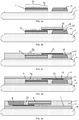
- a temporary carrier substrate 1 having an adhesive layer 2 on its surface, as illustrated in Figure 1a .
- Any type of temporary carrier 1 and adhesive 2 known as suitable for the construction of fan-out wafer level packages may be used, for example a silicon or glass wafer 1 with the adhesive 2 applied thereto by soft baking or spin coating.
- a redistribution layer 3 is produced on the adhesive 2.
- a redistribution layer 3 is similar in structure to the back end of line part of a semiconductor die, comprising one or more levels of metal interconnects embedded in an inorganic or organic dielectric material.
- the term 'redistribution layer' abbreviated RDL, refers to a single layer or to stack of multiple layers as described above.
- the die 4 comprises a semiconductor substrate portion 5 and an active portion 6, with solder bumps 7 on top of the active portion 6.
- the active portion 6 is typically formed of a front end of line part comprising active devices processed on the semiconductor substrate portion 5 and a back end of line part comprising interconnects between the active devices and the solder bumps 7.
- the logic die 4 is bonded to the RDL 3 by bonding the solder bumps 7 of the die to suitable contacts (not shown) on the upper layer of the RDL 3.
- a layer of underfill material 8 is applied, filling the space between the bumps 7.
- the underfill 8 may be applied in any way known in the art, either during bonding of the die 4 or thereafter.
- the die 4 may be provided with planar contact pads or other contact structures known as such in the art.
- the side of the die 4 comprising the bumps 7 or equivalents is referred to as the front side of the die 4.
- the contact bumps 7 or equivalents comprise at least one array of I/O contacts intended to be connected individually to a corresponding array of I/O contacts on a memory die or a stack of memory dies which is/are to be packaged together with the logic die 4, 'individually' meaning that each contact of one array is connected to a corresponding contact of the other array.
- the array of I/O contacts may be a dense array of contacts in accordance with the Wide I/O standard.
- the next step is the creation of two 3-dimensional structures 10 formed of a sacrificial material, on the RDL 3.
- the structures may have a square or rectangular cross-section as seen in a plane parallel to the substrate 1, and are hereafter and in the appended claims referred to as 'blocks'.
- the blocks 10 are produced on either side of the logic die 4.
- the blocks 10 may be produced by 3D printing, stencil printing, lithography and etching or any other suitable technique.
- the sacrificial material is a material that may be removed by wet etching or solvent removal after the structures have been embedded in a mold material, in a manner known as such in the art, for example from the above-cited document US2017/0287736 .
- the sacrificial material may be for example a polymer, a temporary bonding adhesive, or a metal.
- a mold substrate 11 is then produced by a first overmolding step on the adhesive layer 2 in a way known as such from existing wafer level packaging techniques.
- Compression molding or transfer molding may be applied by deposition of a mold compound that is typically a mixture of particles and a thermosetting polymer, for example a thermosetting polymer with >80% silica particles.
- the mold material covers the adhesive layer 2 and envelopes the contours of the die 4 and the blocks 10.
- a post-mold curing step is then applied to obtain a fully set mold substrate 11 embedding the logic die 4 and the blocks 10, i.e. the die 4 and the blocks 10 are fully surrounded laterally and on top by the mold material.
- the mold substrate 11 is then thinned and planarized by a grinding step, as shown in Figure 1e , to a thickness wherein an upper surface of the blocks 10 is exposed, possibly removing an upper layer of the blocks 10.
- a grinding step as shown in Figure 1e , to a thickness wherein an upper surface of the blocks 10 is exposed, possibly removing an upper layer of the blocks 10.
- the back surface of the die 4 is equally exposed by this thinning step, but this is not a limitative requirement of the invention.
- the grinding of a mold substrate is known per se, using for example a tool equipped with a rotatable grinding surface coated with a diamond powder. Other planarization techniques such as chemical mechanical polishing may be used instead of or in addition to the grinding step.
- the sacrificial material of the blocks 10, that is now accessible via the exposed upper surfaces of the blocks, is then removed by a suitable technique, such as by a solvent-aided removal, by heating and melting the sacrificial material, or by etching ( Fig. 1f ).
- a suitable technique such as by a solvent-aided removal, by heating and melting the sacrificial material, or by etching ( Fig. 1f ).
- two openings 12 are created in the mold substrate 11.
- a portion of the RDL 3 is exposed.
- the RDL design and the positioning of the blocks 10 are configured so that at the bottom of each of the openings 12, an array of contacts is exposed after the removal of the blocks 10, the array of contacts being connected individually to the array of I/O contacts on the logic die 4, through the circuitry of the RDL 3.
- the intermediate product shown in Figure 1f is suited for performing a test of the logic die 4.
- the die itself is already embedded in the mold substrate 11, while the contacts for accessing the die via the RDL 3 are exposed at the bottom of the openings 12. An operational test of the die 4 can therefore be performed at this stage without debonding the mold substrate 11 from its carrier.
- the stacks may be DRAM memory die stacks as known in the art.
- Each stack 13 is provided with an array of I/O contacts intended to be individually connected to a corresponding array on the logic die 4, through connections within the RDL 3.
- the die stacks 13 are bonded to the exposed contact arrays at the bottom of the openings 12 in a manner known in the art, possibly including the application of an underfill layer 15, if the I/O contacts on the memory stack and/or the array of contacts on the RDL 3 are provided with solder bumps 14 or other contact structures protruding outward from the surface of the stack 13 and/or the RDL 3.
- the next step is a second overmolding step ( Fig. 1h ), whereby the mold material fills the openings 12 around the memory stacks 13 and forms a second mold substrate 16 on top of the first mold substrate 11, thereby effectively encapsulating the assembly of the logic die 4 and the memory die stacks 13 in a reconstructed wafer formed of the stack of mold substrates 11 and 16 and the RDL 3.
- This is followed by the release of the reconstructed wafer from the adhesive layer 2, and the production of package level solder balls 17 on the underside of the wafer ( Fig. 1i ).
- the reconstructed wafer may be singulated to form separate packages.
- the packages may be singulated prior to releasing them by performing a depth controlled dicing of the reconstructed wafer while it is still attached to the adhesive layer 2. The dicing stops in the adhesive layer 2.
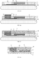
- an additional sacrificial material block 20 is produced on the exposed back surface of the logic die 4, after thinning the first mold substrate 11 and prior to the second overmolding step.
- the second overmolding step then takes place, followed by thinning the second mold substrate 16 until an upper surface of the block 20 is exposed.
- the block 20 is then removed, leaving a cavity 21 above the logic die 4, which may be used for the purpose of cooling the die 4.
- FIGS 3a to 3i illustrate another embodiment of the method of the invention.
- the logic die 4 has now been bonded by attachment of the backside of the die to the adhesive layer 2 on the temporary substrate 1.
- the contact bumps 7a and 7b are directed upward.
- the bumps have been represented as comprising a first set 7a which is an array of I/O contacts destined to be connected individually to corresponding I/O contacts on a memory die or a memory die stack.
- the bumps of the array 7a can be actual bumps of a given height, or equivalent contact structures, such as planar contact pads.
- the remaining contacts 7b are actual bumps which have a non-zero height measured from the front surface of the die 4.
- a block 10 of sacrificial material is produced adjacent the logic die 4, equally attached to the adhesive layer 2.
- the block 10 may be produced by 3D printing or any other suitable technique cited with respect to the previous embodiments.
- the height of the block 10 is as close as possible to the height of the logic die 4, including the height (if any) of the I/O contacts 7a.
- a bridge device 25 is then bonded to the logic die ( Fig. 3b ).
- the bridge device may be a device described as a 'lateral connecting device' in document EP3288076A1 .
- the bridge device 25 comprises two arrays of contacts, respectively on a first and second surface of the bridge device, the first and second surface being on the same side of the bridge device.
- the first and second surface are sub-parts of the front surface of the bridge device.
- Each array has the same number of contacts as the array of I/O contacts 7a on the logic die 4.
- the contacts of the first array of the bridge device are individually connected to corresponding contacts of the second array of the bridge device by circuitry provided in the bridge device 25 itself.
- the bridge device 25 is basically a semiconductor die having a substrate portion 26 and a back end of line portion 27, the latter comprising the interconnecting circuitry between the two contact arrays on the front surface of the bridge device 25.
- the arrays of contacts on the bridge device 25 are arrays of planar contacts in the embodiment shown in the drawings.
- these contacts could be formed of other contact structures such as solder bumps or one array could be planar with the other consisting of solder bumps.
- the bridge device 25 While being bonded to the logic die 4, the bridge device 25 is placed onto the sacrificial block 10, so that any protruding contact structures on the bridge device 25 are embedded into the material of the block 10.
- the sacrificial material is sufficiently soft at the temperature applied during bonding of the bridge device 25 to the logic die 4, so as to allow a degree of embedding of the contact structures of the bridge device 25 in the sacrificial block 10.
- the assembly of the logic die 4, the sacrificial block 10 and the bridge device 25 is now embedded in a first mold substrate 11, by a first overmolding step followed by grinding and planarizing the mold substrate 11 ( Fig. 3c ), which includes thinning the bridge device 25 from the backside.
- the thinning step is done so as to expose the bumps 7b of the logic die 4.
- the height of these bumps must therefore be configured in accordance with the required height of the thinned bridge device 25.
- a redistribution layer 3 is then formed on the thinned mold substrate 11 ( Fig. 3d ), the RDL 3 comprising circuitry connected to the exposed bumps 7b of the logic die 4.
- the assembly of the mold substrate 11 and the RDL 3 is then released from the temporary substrate 1, flipped and bonded to a second temporary substrate 30, provided with a second adhesive 31 ( Fig. 3e ).
- the sacrificial material of the block 10 is then removed by a suitable removal technique in accordance with the type of sacrificial material used ( Fig. 3f ). This creates an opening 32.
- an array of I/O contacts is exposed on the front surface of the bridge device 25.
- the logic die 4 may be tested. If the die 4 passes the tests, a stack 13 of memory dies is bonded to the array of exposed I/O contacts ( Fig. 3g ) at the bottom of opening 32.
- a second overmolding step is then performed, forming a second mold substrate 16 that embeds the memory die stack 13, forming a reconstructed wafer comprising the RDL 3 and the stack of the first and second mold substrates 11 and 16 ( Fig. 3h ).
- the reconstructed wafer is then released from the second temporary substrate 30 and package level solder balls 17 are formed, followed by the singulation of the reconstructed wafer to form a single package ( Fig. 3i ), or alternatively the packages are singulated prior to the release from the second temporary substrate 30.
- the thinning step may be performed by other means instead of by planarization through grinding and/or CMP.
- the thinning could be local, performed by lithography and etching in an area comprising the sacrificial structures which are to be removed. Etching is then performed until an upper surface of such a sacrificial structure is exposed.
- the invention is equally related to a wafer assembly obtainable as an intermediary product of the method of the invention, and that allows testing of the first die 4 prior to mounting the second dies 13.
- This is the assembly illustrated in Figures 1f and 3f for the two embodiments described above.
- the assembly comprises a carrier (1 or 30) onto which a first mold substrate 11 is releasably attached. This includes the possibility of having the mold substrate 11 fixedly attached to an RDL 3 that is itself releasably attached to the carrier.
- the mold substrate 11 comprises the first die 4 embedded therein, and an opening 12 or 32 having contacts at the bottom which are connected to contacts on the die 4.
Landscapes
- Encapsulation Of And Coatings For Semiconductor Or Solid State Devices (AREA)
- Engineering & Computer Science (AREA)
- Manufacturing & Machinery (AREA)
Priority Applications (2)
| Application Number | Priority Date | Filing Date | Title |
|---|---|---|---|
| EP18214441.0A EP3671833A1 (de) | 2018-12-20 | 2018-12-20 | Verfahren zur verpackung von halbleiterchips |
| US16/719,680 US11367705B2 (en) | 2018-12-20 | 2019-12-18 | Method for packaging semiconductor dies |
Applications Claiming Priority (1)
| Application Number | Priority Date | Filing Date | Title |
|---|---|---|---|
| EP18214441.0A EP3671833A1 (de) | 2018-12-20 | 2018-12-20 | Verfahren zur verpackung von halbleiterchips |
Publications (1)
| Publication Number | Publication Date |
|---|---|
| EP3671833A1 true EP3671833A1 (de) | 2020-06-24 |
Family
ID=64870343
Family Applications (1)
| Application Number | Title | Priority Date | Filing Date |
|---|---|---|---|
| EP18214441.0A Pending EP3671833A1 (de) | 2018-12-20 | 2018-12-20 | Verfahren zur verpackung von halbleiterchips |
Country Status (2)
| Country | Link |
|---|---|
| US (1) | US11367705B2 (de) |
| EP (1) | EP3671833A1 (de) |
Cited By (1)
| Publication number | Priority date | Publication date | Assignee | Title |
|---|---|---|---|---|
| CN113394127A (zh) * | 2021-06-16 | 2021-09-14 | 长江存储科技有限责任公司 | 3d存储器桥接结构的关键尺寸的监测方法 |
Families Citing this family (9)
| Publication number | Priority date | Publication date | Assignee | Title |
|---|---|---|---|---|
| US11557541B2 (en) * | 2018-12-28 | 2023-01-17 | Intel Corporation | Interconnect architecture with silicon interposer and EMIB |
| WO2020166567A1 (ja) * | 2019-02-15 | 2020-08-20 | 株式会社村田製作所 | 電子モジュール及び電子モジュールの製造方法 |
| US11410933B2 (en) * | 2020-10-06 | 2022-08-09 | Unimicron Technology Corp. | Package structure and manufacturing method thereof |
| US11721685B2 (en) * | 2021-05-26 | 2023-08-08 | Avago Technologies International Sales Pte. Limited | Copper-bonded memory stacks with copper-bonded interconnection memory systems |
| US12354997B2 (en) * | 2021-08-31 | 2025-07-08 | Taiwan Semiconductor Manufacturing Company, Ltd. | Package structure and manufacturing method thereof |
| US12230622B2 (en) | 2021-10-13 | 2025-02-18 | Mediatek Inc. | Electronic device with stacked printed circuit boards |
| CN116092960A (zh) * | 2021-11-05 | 2023-05-09 | 安徽寒武纪信息科技有限公司 | 晶圆测试的方法、存储介质、计算机程序产品及装置 |
| KR20230143273A (ko) | 2022-04-05 | 2023-10-12 | 삼성전자주식회사 | 반도체 패키지 |
| US20250370202A1 (en) | 2024-06-03 | 2025-12-04 | Celestial Ai Inc. | Packaging optical components in a circuit package |
Citations (5)
| Publication number | Priority date | Publication date | Assignee | Title |
|---|---|---|---|---|
| US20160133571A1 (en) * | 2014-11-07 | 2016-05-12 | Qualcomm Incorporated | Integrated device package comprising silicon bridge in an encapsulation layer |
| US20160358865A1 (en) * | 2015-06-03 | 2016-12-08 | Inotera Memories, Inc. | Wafer level package and fabrication method thereof |
| US20170287736A1 (en) | 2016-03-30 | 2017-10-05 | Sasha Oster | Complex cavity formation in molded packaging structures |
| US9865567B1 (en) * | 2017-02-02 | 2018-01-09 | Xilinx, Inc. | Heterogeneous integration of integrated circuit device and companion device |
| EP3288076A1 (de) | 2016-08-25 | 2018-02-28 | IMEC vzw | Halbleiterchipgehäuse und verfahren zur herstellung des gehäuses |
Family Cites Families (2)
| Publication number | Priority date | Publication date | Assignee | Title |
|---|---|---|---|---|
| US8035224B2 (en) * | 2008-11-14 | 2011-10-11 | Infineon Technologies Ag | Semiconductor device |
| US10438881B2 (en) * | 2015-10-29 | 2019-10-08 | Marvell World Trade Ltd. | Packaging arrangements including high density interconnect bridge |
-
2018
- 2018-12-20 EP EP18214441.0A patent/EP3671833A1/de active Pending
-
2019
- 2019-12-18 US US16/719,680 patent/US11367705B2/en active Active
Patent Citations (5)
| Publication number | Priority date | Publication date | Assignee | Title |
|---|---|---|---|---|
| US20160133571A1 (en) * | 2014-11-07 | 2016-05-12 | Qualcomm Incorporated | Integrated device package comprising silicon bridge in an encapsulation layer |
| US20160358865A1 (en) * | 2015-06-03 | 2016-12-08 | Inotera Memories, Inc. | Wafer level package and fabrication method thereof |
| US20170287736A1 (en) | 2016-03-30 | 2017-10-05 | Sasha Oster | Complex cavity formation in molded packaging structures |
| EP3288076A1 (de) | 2016-08-25 | 2018-02-28 | IMEC vzw | Halbleiterchipgehäuse und verfahren zur herstellung des gehäuses |
| US9865567B1 (en) * | 2017-02-02 | 2018-01-09 | Xilinx, Inc. | Heterogeneous integration of integrated circuit device and companion device |
Non-Patent Citations (1)
| Title |
|---|
| YONGGANG JIN ET AL.: "Next generation eWLB packaging", ELECTRONICS PACKAGING TECHNOLOGY CONFERENCE (EPTC, 2010 |
Cited By (2)
| Publication number | Priority date | Publication date | Assignee | Title |
|---|---|---|---|---|
| CN113394127A (zh) * | 2021-06-16 | 2021-09-14 | 长江存储科技有限责任公司 | 3d存储器桥接结构的关键尺寸的监测方法 |
| CN113394127B (zh) * | 2021-06-16 | 2022-04-19 | 长江存储科技有限责任公司 | 3d存储器桥接结构的关键尺寸的监测方法 |
Also Published As
| Publication number | Publication date |
|---|---|
| US20200203309A1 (en) | 2020-06-25 |
| US11367705B2 (en) | 2022-06-21 |
Similar Documents
| Publication | Publication Date | Title |
|---|---|---|
| US11367705B2 (en) | Method for packaging semiconductor dies | |
| US11854955B2 (en) | Fan-out package with controllable standoff | |
| CN113206059B (zh) | 扇出型硅中介物、芯片封装结构及其形成方法 | |
| US9966325B2 (en) | Semiconductor die package and method of producing the package | |
| CN110660783B (zh) | 半导体器件封装件和方法 | |
| TWI827899B (zh) | 扇出型矽中介物、晶片封裝結構及其形成方法 | |
| US11929261B2 (en) | Semiconductor package and method of manufacturing the same | |
| CN104037153B (zh) | 3d封装件及其形成方法 | |
| TWI497620B (zh) | 矽貫通孔晶粒及封裝 | |
| CN112018065B (zh) | 集成电路器件及其形成方法 | |
| CN110970407A (zh) | 集成电路封装件和方法 | |
| KR20220026996A (ko) | 집적 회로 패키지 및 방법 | |
| CN107546193A (zh) | 积体扇出型封装体 | |
| CN113161302A (zh) | 半导体封装结构、半导体封装件及其制造方法 | |
| US12564054B2 (en) | Package structure | |
| CN105895623B (zh) | 用于半导体封装件的衬底设计及其形成方法 | |
| CN112582389A (zh) | 半导体封装件、封装件及其形成方法 | |
| CN115579341A (zh) | 半导体器件和形成半导体器件方法 | |
| CN113223970A (zh) | 半导体结构及其制造方法 | |
| TW202218069A (zh) | 半導體封裝及製造半導體封裝的方法 | |
| US11177237B2 (en) | Manufacturing method of semiconductor package | |
| CN113078125A (zh) | 管芯堆叠件的形成方法及管芯堆叠结构 | |
| US10283470B2 (en) | Semiconductor package and manufacturing method thereof | |
| US20260144074A1 (en) | Method of manufacturing package structure | |
| US20260144075A1 (en) | Package structure |
Legal Events
| Date | Code | Title | Description |
|---|---|---|---|
| PUAI | Public reference made under article 153(3) epc to a published international application that has entered the european phase |
Free format text: ORIGINAL CODE: 0009012 |
|
| STAA | Information on the status of an ep patent application or granted ep patent |
Free format text: STATUS: THE APPLICATION HAS BEEN PUBLISHED |
|
| AK | Designated contracting states |
Kind code of ref document: A1 Designated state(s): AL AT BE BG CH CY CZ DE DK EE ES FI FR GB GR HR HU IE IS IT LI LT LU LV MC MK MT NL NO PL PT RO RS SE SI SK SM TR |
|
| AX | Request for extension of the european patent |
Extension state: BA ME |
|
| STAA | Information on the status of an ep patent application or granted ep patent |
Free format text: STATUS: REQUEST FOR EXAMINATION WAS MADE |
|
| 17P | Request for examination filed |
Effective date: 20201106 |
|
| RBV | Designated contracting states (corrected) |
Designated state(s): AL AT BE BG CH CY CZ DE DK EE ES FI FR GB GR HR HU IE IS IT LI LT LU LV MC MK MT NL NO PL PT RO RS SE SI SK SM TR |