EP3660883A2 - Charged particle multi-beamlet apparatus - Google Patents
Charged particle multi-beamlet apparatus Download PDFInfo
- Publication number
- EP3660883A2 EP3660883A2 EP19216208.9A EP19216208A EP3660883A2 EP 3660883 A2 EP3660883 A2 EP 3660883A2 EP 19216208 A EP19216208 A EP 19216208A EP 3660883 A2 EP3660883 A2 EP 3660883A2
- Authority
- EP
- European Patent Office
- Prior art keywords
- electrodes
- charged particle
- opening
- manipulator device
- beamlets
- Prior art date
- Legal status (The legal status is an assumption and is not a legal conclusion. Google has not performed a legal analysis and makes no representation as to the accuracy of the status listed.)
- Granted
Links
Images


Classifications
-
- H—ELECTRICITY
- H01—ELECTRIC ELEMENTS
- H01J—ELECTRIC DISCHARGE TUBES OR DISCHARGE LAMPS
- H01J37/00—Discharge tubes with provision for introducing objects or material to be exposed to the discharge, e.g. for the purpose of examination or processing thereof
- H01J37/30—Electron-beam or ion-beam tubes for localised treatment of objects
- H01J37/3002—Details
- H01J37/3007—Electron or ion-optical systems
-
- B—PERFORMING OPERATIONS; TRANSPORTING
- B82—NANOTECHNOLOGY
- B82Y—SPECIFIC USES OR APPLICATIONS OF NANOSTRUCTURES; MEASUREMENT OR ANALYSIS OF NANOSTRUCTURES; MANUFACTURE OR TREATMENT OF NANOSTRUCTURES
- B82Y10/00—Nanotechnology for information processing, storage or transmission, e.g. quantum computing or single electron logic
-
- B—PERFORMING OPERATIONS; TRANSPORTING
- B82—NANOTECHNOLOGY
- B82Y—SPECIFIC USES OR APPLICATIONS OF NANOSTRUCTURES; MEASUREMENT OR ANALYSIS OF NANOSTRUCTURES; MANUFACTURE OR TREATMENT OF NANOSTRUCTURES
- B82Y40/00—Manufacture or treatment of nanostructures
-
- H—ELECTRICITY
- H01—ELECTRIC ELEMENTS
- H01J—ELECTRIC DISCHARGE TUBES OR DISCHARGE LAMPS
- H01J37/00—Discharge tubes with provision for introducing objects or material to be exposed to the discharge, e.g. for the purpose of examination or processing thereof
- H01J37/30—Electron-beam or ion-beam tubes for localised treatment of objects
- H01J37/317—Electron-beam or ion-beam tubes for localised treatment of objects for changing properties of the objects or for applying thin layers thereon, e.g. for ion implantation
- H01J37/3174—Particle-beam lithography, e.g. electron beam lithography
-
- H—ELECTRICITY
- H01—ELECTRIC ELEMENTS
- H01J—ELECTRIC DISCHARGE TUBES OR DISCHARGE LAMPS
- H01J37/00—Discharge tubes with provision for introducing objects or material to be exposed to the discharge, e.g. for the purpose of examination or processing thereof
- H01J37/30—Electron-beam or ion-beam tubes for localised treatment of objects
- H01J37/317—Electron-beam or ion-beam tubes for localised treatment of objects for changing properties of the objects or for applying thin layers thereon, e.g. for ion implantation
- H01J37/3174—Particle-beam lithography, e.g. electron beam lithography
- H01J37/3177—Multi-beam, e.g. fly's eye, comb probe
-
- H—ELECTRICITY
- H01—ELECTRIC ELEMENTS
- H01J—ELECTRIC DISCHARGE TUBES OR DISCHARGE LAMPS
- H01J2237/00—Discharge tubes exposing object to beam, e.g. for analysis treatment, etching, imaging
- H01J2237/04—Means for controlling the discharge
- H01J2237/043—Beam blanking
- H01J2237/0435—Multi-aperture
-
- H—ELECTRICITY
- H01—ELECTRIC ELEMENTS
- H01J—ELECTRIC DISCHARGE TUBES OR DISCHARGE LAMPS
- H01J2237/00—Discharge tubes exposing object to beam, e.g. for analysis treatment, etching, imaging
- H01J2237/04—Means for controlling the discharge
- H01J2237/049—Focusing means
- H01J2237/0492—Lens systems
- H01J2237/04924—Lens systems electrostatic
-
- H—ELECTRICITY
- H01—ELECTRIC ELEMENTS
- H01J—ELECTRIC DISCHARGE TUBES OR DISCHARGE LAMPS
- H01J2237/00—Discharge tubes exposing object to beam, e.g. for analysis treatment, etching, imaging
- H01J2237/10—Lenses
- H01J2237/12—Lenses electrostatic
- H01J2237/1205—Microlenses
-
- H—ELECTRICITY
- H01—ELECTRIC ELEMENTS
- H01J—ELECTRIC DISCHARGE TUBES OR DISCHARGE LAMPS
- H01J2237/00—Discharge tubes exposing object to beam, e.g. for analysis treatment, etching, imaging
- H01J2237/15—Means for deflecting or directing discharge
-
- H—ELECTRICITY
- H01—ELECTRIC ELEMENTS
- H01J—ELECTRIC DISCHARGE TUBES OR DISCHARGE LAMPS
- H01J2237/00—Discharge tubes exposing object to beam, e.g. for analysis treatment, etching, imaging
- H01J2237/153—Correcting image defects, e.g. stigmators
- H01J2237/1532—Astigmatism
-
- H—ELECTRICITY
- H01—ELECTRIC ELEMENTS
- H01J—ELECTRIC DISCHARGE TUBES OR DISCHARGE LAMPS
- H01J37/00—Discharge tubes with provision for introducing objects or material to be exposed to the discharge, e.g. for the purpose of examination or processing thereof
- H01J37/30—Electron-beam or ion-beam tubes for localised treatment of objects
- H01J37/317—Electron-beam or ion-beam tubes for localised treatment of objects for changing properties of the objects or for applying thin layers thereon, e.g. for ion implantation
Definitions
- the invention relates to a method for influencing and/or controlling the trajectory of one or more charged particle beamlets in a charged particle multi-beamlet apparatus.
- the invention more specifically relates to a charged particle multi-beamlet apparatus using a plurality of charged particle beamlets, said apparatus comprises a manipulator device for manipulation of one or more charged particle beams of the plurality of charged particle beamlets.
- a manipulator device for manipulation of one or more charged particle beams of the plurality of charged particle beamlets.
- multi electron beam systems are being developed for high throughput maskless lithography systems, multi electron beam microscopy and multi electron beam induced deposition devices.
- the invention further relates to a maskless charged particle multi-beamlet lithography system, a charged particle multi-beamlet microscopy system, a charged particle multi-beamlet beam induced deposition device, and a manipulator device for use in a charged particle multi-beamlet apparatus.
- a charged particle multi-beamlet lithography system for exposing a target using a plurality of beamlets is disclosed for example in WO 2009/127659 A2 .
- the lithography device comprises a deflection device comprising a plurality of deflectors, wherein the deflection device comprises a plurality of memory cells, each cell being provided with a storage element and being connected to a deflector.
- the storage element is effectively used as a control signal of a locally available amplifier, which provides a substantially digital signal to the deflectors.
- the deflector is either on or off. This is a very important step for obtaining a high accuracy of the patterning step of the lithography system, and a high wafer throughput.
- the present invention aims to provide a manipulator device and a charged particle multi-beamlet apparatus comprising such a manipulator device enabling an improved manipulation of individual beamlets of said plurality of beamlets.
- the invention provides a method for influencing and/or controlling the trajectory of one or more charged particle beamlets in a charged particle multi-beamlet apparatus, wherein said apparatus comprises a manipulator device for manipulation of one or more charged particle beams of a plurality of charged particle beamlets in the charged particle multi-beamlet apparatus, wherein the manipulator device comprises:
- an electrostatic field can be generated which field can be used for influencing and/or controlling the trajectory of the charged particle in a charged particle beamlet.
- the manipulator device of the present invention is able to provide an individual adjustable voltage control for the electrodes of each individual through opening.
- the voltage can be set at various different levels for each individual through opening, providing individual adjustment control for each beamlet.
- the voltage is individual adjustable for each electrode.
- the charged particle multi-beamlet apparatus comprises a sensor for determining at least one characteristic of said charged particle beamlets, wherein the sensor is connected to said electronic control circuit, wherein the method comprises the step of providing individual adjustment control for each through opening based on a feedback signal provided by the sensor to the electronic control circuit.
- the alignment of the individual beamlets is periodically checked, for example each time during the exchange of a target in a lithography system, the beamlets are checked using the sensor and the control circuit adjusts the control signals in order to provide corrected settings for the manipulator device to at least substantially correct for a deterioration and/or drift of one or more of the individual beamlets. Subsequently, the corrected setting of the manipulator device is maintained during the processing of the subsequent target.
- the combination of manipulator, control circuit and sensor also enables a feedback system for adjusting and/or optimizing each beamlet and/or the alignment of each beamlet individually in a charged particle multi-beamlet apparatus, in particular a multi-beamlet charged particle lithography system.
- the feedback system is arranged for dynamically adjusting and/or optimizing each beamlet and/or the alignment of each beamlet individually.
- This feedback system is preferably arranged, preferably as a whole, in the charged particle multi-beamlet apparatus, in particular in the multi-beamlet charged particle lithography system.
- the manipulator device is arranged for focusing, deflection or stigmation (in particular reducing astigmatism) of individual beamlets of said plurality of beamlets.
- the improved manipulator device of the invention can be used for manipulation of individual beamlets of said plurality of beamlets not only for deflecting individual beamlets, but also for other functions, such as individual focusing of beamlets or astigmatism correction of individual beamlets, as will be apparent from the description of the embodiments below.
- the electronic control circuit is arranged for providing each of the one or more electrodes of each individual through opening with an at least substantially analog adjustable voltage.
- an adjustable voltage small corrections can be made to each beamlet, for example for a correction of the angle of deflection, for adjusting the strength of an electrostatic lenslet or for providing a correction for astigmatism, in order to optimize the plurality of beamlets.
- the electronic control circuit is at least partially arranged on the planar substrate and at least partially adjacent to said through openings.
- each through opening is arranged for providing a passage for one single beamlet.
- each through opening is arranged for providing a passage for several beamlets, for example a group of 7 x 7 beamlets.
- the planar substrate is a wafer
- the electronic control circuit comprises an integrated circuit on said planar substrate.
- the electronic control circuit is at least partially arranged in-between two through openings.
- the control circuit is arranged near the actual trough openings with the one or more electrodes. In particular between through openings, more particular in non-beam areas between two groups op through openings, the electronic control circuit can be suitably arranged.
- the electronic control circuit comprises a memory for storing control data for the one or more electrodes of one or more individual through openings, which memory is arranged on the planar substrate and adjacent to said through openings.
- said memory is arranged for storing control data for setting the voltage at various different levels for each individual through opening.
- the memory is arranged for storing control data for the one or more electrodes of one individual through opening, which memory is arranged on the planar substrate and adjacent to said individual through opening. In one embodiment, the memory is arranged in-between two through openings.
- the one or more electrodes comprise a metal that is deposited on the planar substrate.
- the metal comprises Molybdenum.
- the one or more electrodes are arranged in and/or on said substrate. In one embodiment, the through openings extend at least substantially transverse to a surface of said substrate.
- the one or more electrodes of a through opening are at least partially arranged against an inwards facing wall of said through opening. In one embodiment, said one or more electrodes extend into the trough opening in a direction substantially parallel a centre line of said through opening. Such electrodes can provide a more homogeneous electrostatic field for more accurate manipulating the charged particles in a beamlet.
- the one or more electrodes of each through opening are at least substantially surrounded by an earthed electrode.
- the earthed electrode comprises a metal that is deposited on the planar substrate.
- the metal comprises Molybdenum. Since the individual through openings and their electrodes are arranged at close proximity, the surrounding earthed electrode at least reduces crosstalk.
- a surface of the one or more electrodes that faces away from the planar substrate is arranged at a height between the planar substrate and a surface of the earthed electrode that faces away from said planar substrate.
- a thickness of the earthed electrode on the planar substrate is larger than a thickness of the one or more electrodes on the planar substrate.
- the one or more electrodes are arranged at a recessed location with respect to the surrounding earthed electrode. The higher level of the surrounding earthed electrode with respect to the level of the one or more electrodes at a through opening further reduces any crosstalk between the one or more electrodes of adjacent through openings.
- the higher level of the surrounding earthed electrode with respect to the level of the one or more electrodes at a through opening reduces beam errors due to electrostatic stray fields.
- the electronic control circuit comprises connecting leads for connecting the electronic control circuit with the one or more electrodes, wherein at least one of said connecting leads is at least partially arranged between two earthed electrically conducting layers. In one embodiment, the at least one of said connecting leads is at least partially arranged between two earthed leads. By arranging at least some of the connecting leads, at least partially between conducting layers and/or leads, said leads are shielded which reduces any interference between the connecting leads.
- said manipulator device comprises an array of electrostatic lenses, wherein each of said electrostatic lenses comprises one through opening of said array of through openings, wherein each of the through openings comprises one electrode arranged around the corresponding through opening, and wherein the electronic control circuit is arranged for providing the one electrode of each individual through opening of a lens of said array of electrostatic lenses with an adjustable voltage for individually adjusting a strength of said lens.
- said manipulator device comprises an array of electrostatic deflectors, wherein each of said electrostatic deflectors comprises one through opening of said array of through openings, wherein each of the through openings comprises two or more electrodes arranged around the corresponding through opening, and wherein the electronic control circuit is arranged for providing the two or more electrodes of each individual through opening of a deflector of said array of electrostatic deflectors with an adjustable voltage for individually adjusting an amount of deflection of a charged particle beamlet induced by said deflector.
- said manipulator device comprises an array of electrostatic astigmatic correctors, wherein each of said electrostatic astigmatic correctors comprises one through opening of said array of through openings, wherein each of the through openings comprises eight electrodes arranged around the corresponding through opening, and wherein the electronic control circuit is arranged for providing the eight electrodes of each individual through opening of an astigmatic corrector of said array of electrostatic astigmatic correctors with an adjustable voltage for individually adjusting an amount of astigmatism correction of a charged particle beamlet induced by said astigmatic corrector.
- the electronic control circuit comprises a demultiplexer for extracting control data for one or more individual through openings from a multiplexed signal, which demultiplexer is arranged on the planar substrate and adjacent to said through openings.
- the demultiplexer is arranged for extracting control data for the one or more electrodes of one individual through opening, which demultiplexer is arranged on the planar substrate and adjacent to said individual through opening.
- the demultiplexer is arranged in-between adjacent through openings.
- the number of connecting leads to the device is substantially smaller than the number of electrodes. In one embodiment, the number of connecting leads to a through opening is smaller than the number of electrodes of said through opening.
- the invention provides a charged particle multi-beamlet apparatus comprising a manipulator device for manipulation of one or more charged particle beams of a plurality of charged particle beamlets in the charged particle multi-beamlet apparatus, wherein the manipulator device comprises:
- the charged particle multi-beamlet apparatus further comprises a sensor for determining at least one characteristic of said plurality of charged particle beamlets, wherein the sensor is connected to said electronic control circuit for providing a feedback signal.
- a feedback arrangement is particularly advantageous in a multi-beamlet system in order to enable an automated feedback for the individually adjustable voltages of each of the one or more electrodes of each of the individual through openings, for setting each of the adjustable voltages to a required value for obtaining the desired correction of each beamlet of said plurality of charged particle beamlets.
- the manipulator device is a first manipulator device having a first planar substrate comprising a first array of through openings in the plane of the first planar substrate
- the charged particle beam apparatus comprises a second manipulator device having a second planar substrate comprising a second array of through openings in the plane of the second planar substrate, wherein each of the through openings comprises one or more electrodes arranged around the corresponding through opening, and wherein the one or more electrodes are arranged in and/or on said substrate
- the second planar substrate is arranged at a distance and substantially parallel to the first planar substrate, wherein each through opening of the second array of through openings are at least substantially in line with a through opening of the first array of through opening.
- the through openings have a radius r, and wherein the distance d between the first and second planar substrate is equal or smaller than the radius r.
- the one or more electrodes of the first and second manipulator device are arranged on said first and second substrate, respectively, and wherein the one or more electrodes on the first substrate and the one or more electrodes on the second substrate face each other.
- the second manipulator device is at least substantially mirror symmetrical to the first manipulator device, at least with respect to a centre plane between the first and second manipulator device.
- the invention provides a charged particle multi-beamlet maskless lithography device comprising a manipulator device for manipulation of one or more charged particle beams of a plurality of charged particle beamlets in the charged particle multi-beamlet maskless lithography device, wherein the manipulator device comprises:
- the charged particle multi-beamlet maskless lithography device and/or the manipulator device thereof is provided with one or more of the measures described in the above mentioned embodiments.
- the invention provides a manipulator device for manipulation of one or more charged particle beams of a plurality of charged particle beamlets in a charged particle multi-beamlet apparatus, wherein the manipulator device comprises:
- the manipulator device is provided with one or more of the measures described in the above mentioned embodiments.
- Multi-electron beam systems are being developed for high throughput lithography, multi-electron beam microscopy and multi-electron bean induced deposition.
- individual beam blanking that is on or off switching, is used for patterning.
- the present invention proposes to uses MEMS technology for the manufacturing of manipulator devices comprising an array of manipulators for manipulating one or more charged particle beamlets of a plurality of charged particle beamlets.
- the manipulators preferably have lateral sizes ranging form approximately 150 micrometers to 2 micrometers, depending on their purpose.
- One of the challenges is to design electrodes with a fabrication process that is compatible with chip fabrication and electron optical design rules. Furthermore it is desirable to control thousands of beams without having thousands of external control wires.
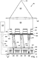
- FIG. 1 shows a schematic drawing of a charged particle mulit-beamlet lithography device 100 based upon a charged particle beam optical system without a common crossover of all the charged particle beamlets.
- a lithography system comprises a charged particle source 101, for example an electron source, for producing an expanding charged particle beam 120.
- the expanding beam passes a collimator lens 102 for collimating the charged particle beam 120.
- the collimated beam 120 impinges on an aperture array 104, which blocks part of the collimated beam 120 for creating sub-beams 121.
- the sub-beams 121 impinge on a further aperture array 105 for creating beamlets 122.
- a condenser lens array 103 (or set of condenser lens arrays) is included for focusing the sub-beams 121 towards a corresponding opening in the beam stop array 108 of end module 107.
- the beamlet creating aperture array 105 is preferably included in combination with a beamlet blanker array 106, for example arranged close together with aperture array 105 before the blanker array 106.
- the condenser lens or lenses 103 focus sub-beam 121 either in or towards a corresponding opening in beam stop array 108 of end module 107.
- the aperture array 105 produces three beamlets 122 from sub-beam 121, which strike the beam stop array 108 at a corresponding opening so that the three beamlets 122 are projected onto the target 110 by the projection lens system 109 in end module 107.
- a group of beamlets with a much larger number of beamlets may be produced by aperture array 105 for each projection lens system 109 in end module 107.
- typically around fifty beamlets may be directed through a single projection lens system 109, and this may be increased to two hundred or more.
- the beamlet blanker array 106 may deflect individual beamlets in a group of beamlets 122 at certain times in order to blank them. This is illustrated by blanked beamlet 123, which has been deflected to a location on the beam stop array 108 near to but not at an opening.
- the charged particle optical column may be provided with one or more manipulator devices as described in more detail below.
- a manipulator device 300 may be arranged behind the collimator lens 102 for:
- Such a manipulator device 310 may also be provided as part of the end module 107 for providing a two dimensional deflection in the projection lens system 109 and enabling a vector scan of the beamlets in one group.
- the manipulator device 300, 310 is connected to an electronic control circuit 430, which provides control signals 433, 434 to the manipulator device 300, 310.
- the charged particle optical column is provided with a sensor for determining at least one characteristics of a beamlet of the plurality of beamlets, wherein the sensor is connected to the electronic control circuit 430 in order to provide a feedback signal.
- a sensor 410 can be provided at the beam stop array 108, preferably at the location where the beamlets are directed when blanked.
- a sensor 420 can be arranged substantially at the location of the target 110 during an exchange of a target which has been process and a target that needs to be processed.
- the detector 420 can be moved XY under the beamlets and the alignment of the beamlets can be checked and if necessary the manipulator devices 300, 310 can be -preferably automatically - adjusted based on the feedback signal 431, 432 provided by the sensor 410, 420 to the electronic control circuit 430.
- any deterioration and/or drift in the alignment of the beamlets 122 occurs at a very slow pace when compared with the deflection of the beamlets 122 by the beamlet blanker array 106.
- the beamlets 122 are checked using the sensors 410, 420 and the control circuit 430 adjusts the control signals 433, 434 in order to provide corrected settings for the manipulator devices 300, 310 to at least substantially correct for a deterioration and/of drift of one or more of the individual beamlets 122.
- the corrected setting of the manipulator devices 300, 310 is maintained during the processing of the subsequent target.
- the combination of manipulator 300, control circuit 430 and sensors 410, 420 also provides a feedback system for adjusting and/or optimizing each beamlet and/or the alignment of each beamlet individually in a charged particle multi-beamlet apparatus, in particular a multi-beamlet charged particle lithography system.
- the feedback system is arranged for dynamically adjusting and/or optimizing each beamlet and/or the alignment of each beamlet individually.
- This feedback system is preferably arranged, preferably as a whole, in the charged particle multi-beamlet apparatus, in particular in the multi-beamlet charged particle lithography system.
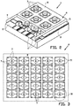
- FIG. 2 shows a multi-beamlet quadropole deflector 1, which has been manufactured using MEMS technology.
- the fabrication process is bipolar compatible allowing local electronics to be incorporated, for example enabling sample and hold functionality.
- the multi-beamlet quadrupole deflector 1 comprises a substantially planar substrate 3, which is provided with an array of through openings 2 which are regularly arranged in rows and columns.
- the through openings 2 extend substantially transverse to the surface S of the planar substrate 3, and are arranged for passing at least one charged particle beamlet there through.
- an electronic control circuit 4 On top of the planar substrate 3, which in this example is a Si chip, an electronic control circuit 4 is arranged.
- the electronic control circuit 4 comprises an integrated circuit which has been arranged adjacent to the through openings 2, in particularly on non-beam areas of the planar substrate 3.
- an insulating layer 5 is provided, on top op which insulating layer 5, an electrode layer 6 is arranged.
- Each of the through openings 2 is provided with four electrodes 7 arranged around the through opening 2 on said substrate 3.
- Each through opening 2 with its four electrodes 7 forms an individual manipulator 10 for manipulating one or more beamlets which traverse the through opening 2.
- the manipulator device 1 comprises an array of individual manipulators 10 which are arranged in rows and columns.
- the electrodes 7 are preferably made from Molybdenum, however they may also be made from other conducting materials.
- the electrode layer 6 is approximately 4 micrometers thick, and the electrodes have been made by anisotropic etching of the Molybdenum using reactive ion etching.
- the four electrodes 7 are surrounded by a remaining part 8 of the electrode layer 6, as shown in the schematic top view of figure 2 .
- This remaining part 8, which is electrically isolated from the electrodes 7, is used as an earthed electrode 8 which surrounds the four electrodes 7 at a distance.
- the electronic control circuit 4 provides control signals to each of the four electrodes 7 of each through opening 2.
- the electronic control circuit 4 is arranged on the planar substrate 3 and at least partially adjacent to said through openings 2, and is arranged for providing each of the four electrodes 7 of each through opening 2 with an individual adjustable voltage for deflecting one or more charged particle beamlet which, when in use, traverse through said opening 2.
- Each manipulator 10 of said manipulator device 1 thus can be used for deflecting the charged particle beamlet in any direction in a plane parallel to the surface S of the planar substrate 3, with an adjustable voltage for individually adjusting an amount of deflection of a charged particle beamlet induced by said deflector 10.
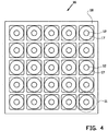
- Figures 4 and 5 show a second example of a manipulator 11 for use in a device of the invention.
- the manipulator device of this second example comprises the same structure as the device shown in the exploded view of figure 2 . That is, the device comprises a substantially planar substrate 13, which is provided with an array of through openings 12 which are regularly arranged in rows and columns, as shown in the top view of figure 4 .
- the through openings 12 are arranged for passing at least one charged particle beamlet there through, and are provided with one electrode 17 which surrounds the through opening 12.
- the electronic control circuit 14 comprises an integrated circuit which has been arranged adjacent to the through openings 12.
- the electronic control circuit 14 is built up from several layers 15 with integrated electronic circuitry, which are interconnected with via's 51.
- via's 52 are provided, which via's 52 are connected to the top electrode 17.
- the via's 52 provide an extension of the top electrode 17 inside the through opening 12.
- the via's 52 at the edge of the through openings 12 are manufactured at the same time and using the same process used for the manufacture of the integrated electronic control circuit 14.
- Each of the through openings 12 is provided with one electrodes 17 arranged around the through opening 12 on said substrate 13. At a distance above the planer substrate 13, a further electrode 19 is arranged.
- the further electrode 19 also comprises an array of through openings 12', which are aligned with the trough openings 12 of the substrate 13, as schematically shown in the cross section in figure 5 .
- Each through opening 12 with its electrode 17 and the further electrode 19 forms an individual Einzel lens 11, which in use is provided with an adjustable voltage for individually adjusting a focal distance or strength of said lens 11.
- This second example thus provides a manipulator device 16 comprises an array of electrostatic lenses 11, wherein each of said electrostatic lenses 11 comprises one through opening 12 of said array of through openings, wherein each of the through openings 12 comprises one electrode 17 arranged around the corresponding through opening 12, and wherein the electronic control circuit 14 is arranged for providing the one electrode 12 of each individual through opening of a lens 11 of said array of electrostatic lenses with an adjustable voltage for individually adjusting a strength of said lens 11.
- FIG. 6 shows a third example of a manipulator device 20 of the invention.
- the manipulator device 20 of this third example comprises the same structure as the device shown in the exploded view of figure 2 . That is, the device comprises a substantially planar substrate, which is provided with an array of through openings 22 which are regularly arranged in rows and columns, as shown in the top view of figure 6 .
- the through openings 22 are arranged for passing at least one charged particle beamlet there through.
- Each through opening 22 is provided with eight electrodes 27 which surround the through opening 12.
- Each through opening 12 with its electrodes 17 forms an individual octopole deflector, which in use is provided with an adjustable voltage for individually adjusting a trajectory of beamlets which traverse one of said through openings 12, for example for providing a stigmatic correction for each individual beamlet.
- the manipulator device 20 of this third example comprises an array of electrostatic stigmatic correctors 21, for example for correcting any astigmatism of the beamlets, wherein each of said electrostatic stigmatic correctors 21 comprises one through opening 22 of said array of through openings, wherein each of the through openings 22 comprises eight electrodes 27 arranged around the corresponding through opening 22, and wherein the electronic control circuit is arranged for providing the eight electrodes 27 of each individual through opening 22 of a stigmatic corrector 21 of said array of electrostatic stigmatic correctors with an adjustable voltage for individually adjusting an amount of stigmatism correction of a charged particle beamlet induced by said stigmatic corrector.
- the device 31 comprises a first manipulator device 30 having a first planar substrate 33 comprising a first array of through openings 32 in the plane of the first planar substrate 33, wherein each of the through openings 32 comprises one or more electrodes 37 arranged around the corresponding through opening 32, and wherein the one or more electrodes 37 are arranged on said substrate 33.
- the device 31 comprises a second manipulator device 30' having a second planar substrate 33' comprising a second array of through openings 32' in the plane of the second planar substrate, wherein each of the through openings 32' comprises one or more electrodes 37' arranged around the corresponding through opening 32', and wherein the one or more electrodes 32' are arranged on said substrate 33'.
- the second planar substrate 33' is arranged at a distance d and substantially parallel to the first planar substrate 33, wherein each through opening 32' of the second manipulator device 30' is at least substantially in line with a through opening 32 of the first manipulator device 30.
- the first 30 and second 30' manipulator devices are formed as one unit.
- the through openings 32, 32' have a radius r, and the distance d between the first and second planar substrate is suitably equal or smaller than the radius r.
- the one or more electrodes 37, 73' of the first 30 and second 30' manipulator device are arranged on said first 33 and second 33' substrate, such that the one or more electrodes 37 on the first substrate 33 and the one or more electrodes 37' on the second substrate 33' face each other.
- the second manipulator device 30' is at least substantially mirror symmetrical to the first manipulator device 30, at least with respect to a centre plane between the first 30 and second 30' manipulator device in order to combine each through opening 32 of the first manipulator device 30 with a corresponding through opening 32' of the second manipulator device 30'.
- Each of the first 30 or second 30' manipulator devices may comprise an array of deflectors having two or more electrodes 37, 37' for each through opening 32, 32', for example four electrodes as shown in figures 2 and 3 , an array of electrostatic lenses having on electrode 37, 37' for each through opening 32, 32', as shown in figure 4 , and/or an array of electrostatic stigmatic correctors having eight electrodes 37, 37' for each through opening 32, 32', as shown in figure 6 .
- the beamlets 122 are arranged groups. Due to the grouping of the beamlets 122, the devices of charged particle optical column after the aperture array 104, which blocks part of the collimated beam 120 for creating sub-beams 121, can be divided in beam areas 200 and non-beam 210 areas, as schematically depicted in figure 8A . These non-beam areas 210, which are located between groups of beamlets, for example as defined by the sub-beams 121, can be used as a location for the electronic control circuit 510 which controls the manipulators 520 arranged in the beam areas 200, as schematically shown in figure 8B .
- connectors 500 are provided, which are connected to the electronic control circuits 510 for each manipulator 520 in the beam area 200, using data lines. From each electronic control circuit 510 voltage lines are directed to the individual electrodes of each manipulator 520 for providing each electrode with an individual adjustable voltage.
- the non-beam areas 210 enough room is available for arranging memory devices of the integrated electronic control circuit for storing control data for the manipulator devices arranged in the adjacent beam area 200.
- the memories are arranged for storing control data for setting the voltage at various different levels for each individual manipulator 520.
- a demultiplexer is arranged in the non-beam areas 210 for demultiplexing a multiplexed data signal and transmitting the demultiplexed data to the electronic control circuit and/or the memory devices thereof.
- Such an embodiment requires substantially one data lead per non-beam area 201, which dramatically reduces the number of connecting leads.
- FIG. 9 shows a schematic cross section of a charged particle multi-beamlet inspection apparatus for measuring beam properties of individual beamlets.
- the charged particle multi-beamlet inspection apparatus comprises entrance aperture array 1050 which, in use, is aligned with a group of beamlets 1220 so that these beamlets 1220 enter the inspection apparatus.
- the inspection apparatus comprises a manipulator device 3000 comprising individual beamlet manipulators 2, 22, as for example shown in figure 2, 3 and 6 , for individually deflecting one or more of the beamlets 1220 in accordance with a control signal 4330 from a controller 4300.
- a series of sensors 4100, 4101, 4200 are arranged.
- the series of sensors comprises a central sensor 4200 which comprises a Faraday cup.
- the controller 4300 provides control signals 4330 to the individual beamlet manipulators of the manipulator device 3000 to deflect all beamlets 1220 into the Faraday cup 4200, the total current of the charged particle beamlets 1220 is measured.
- a measuring signal 4310 of the measurement of the Faraday cup 4200 is directed to the controller 4300 and can be displayed, stored and/or further evaluated in the controller 4300.
- the central censor 4200 is surrounded by several sensors 4100, 4101 for measuring beam properties of individual beamlets 1230.
- the controller 4300 provides a control signal 4330 in order to deflect the individual beamlet 1230 onto one of the sensors 4100.
- the manipulation device 3000 comprises individual deflectors 2 as shown in figures 2, 3
- the individual beamlets 1230 can be deflected in any direction and the amount of deflection in a certain direction can be individually adjusted.
- each individual beamlet 1230 can be subsequently directed to two or more sensors 4100, 4101 in order to measure different beam properties.
- one of the two or more sensors 4100, 4101 is arranged for measuring the total current of the individual beamlet 1230
- a second sensor of the two or more sensors 4100, 4101 is arranged for measuring a first beam profile while the individual beamlet 1230 is scanned in a first direction over the second sensor
- a third sensor of the two or more sensors 4100, 4101 is arranged for measuring a second beam profile while the individual beamlet 1230 is scanned in a second direction, which is at least substantially perpendicular to the first direction, over the third sensor.
- a measuring signal 4320 of the measurement of the sensors 4100, 4101 is directed to the controller 4300 and can be displayed, stored and/or further evaluated in the controller 4300.
- the present invention relates to a method and a device for manipulation of one or more charged particle beams of a plurality of charged particle beamlets in a charged particle multi-beamlet apparatus.
- the manipulator device comprises a planar substrate comprising an array of through openings in the plane of the substrate, each of these through openings is arranged for passing the at least one charged particle beamlet there through, wherein each of the through openings is provided with one or more electrodes arranged around the through opening, and a electronic control circuit for providing control signals to the one or more electrodes of each through opening, wherein the electronic control circuit is arranged for providing the one or more electrodes of each individual through opening with an at least substantially analog adjustable voltage.
Landscapes
- Chemical & Material Sciences (AREA)
- Engineering & Computer Science (AREA)
- Nanotechnology (AREA)
- Analytical Chemistry (AREA)
- Physics & Mathematics (AREA)
- Crystallography & Structural Chemistry (AREA)
- Mathematical Physics (AREA)
- Theoretical Computer Science (AREA)
- Condensed Matter Physics & Semiconductors (AREA)
- General Physics & Mathematics (AREA)
- Manufacturing & Machinery (AREA)
- Electron Beam Exposure (AREA)
Abstract
Description
- The invention relates to a method for influencing and/or controlling the trajectory of one or more charged particle beamlets in a charged particle multi-beamlet apparatus.
- The invention more specifically relates to a charged particle multi-beamlet apparatus using a plurality of charged particle beamlets, said apparatus comprises a manipulator device for manipulation of one or more charged particle beams of the plurality of charged particle beamlets. For example, multi electron beam systems are being developed for high throughput maskless lithography systems, multi electron beam microscopy and multi electron beam induced deposition devices.
- The invention further relates to a maskless charged particle multi-beamlet lithography system, a charged particle multi-beamlet microscopy system, a charged particle multi-beamlet beam induced deposition device, and a manipulator device for use in a charged particle multi-beamlet apparatus.
- A charged particle multi-beamlet lithography system for exposing a target using a plurality of beamlets is disclosed for example in
WO 2009/127659 A2 . The lithography device comprises a deflection device comprising a plurality of deflectors, wherein the deflection device comprises a plurality of memory cells, each cell being provided with a storage element and being connected to a deflector. The storage element is effectively used as a control signal of a locally available amplifier, which provides a substantially digital signal to the deflectors. In other words, the deflector is either on or off. This is a very important step for obtaining a high accuracy of the patterning step of the lithography system, and a high wafer throughput. - The present invention aims to provide a manipulator device and a charged particle multi-beamlet apparatus comprising such a manipulator device enabling an improved manipulation of individual beamlets of said plurality of beamlets.
- According to a first aspect, the invention provides a method for influencing and/or controlling the trajectory of one or more charged particle beamlets in a charged particle multi-beamlet apparatus, wherein said apparatus comprises a manipulator device for manipulation of one or more charged particle beams of a plurality of charged particle beamlets in the charged particle multi-beamlet apparatus, wherein the manipulator device comprises:
- a planar substrate comprising an array of through openings in the plane of the substrate, each of these through openings is arranged for passing at least one charged particle beamlet there through, wherein each of the through openings is provided with one or more electrodes arranged around the through opening, and wherein the one or more electrodes are arranged in and/or on said substrate, and
- an electronic control circuit for providing control signals to the one or more electrodes of each through opening of the array of through openings,
- wherein the method comprises the step of providing individual adjustment control for each through opening by providing the one or more electrodes of each individual through opening with an at least substantially analog adjustable voltage.
- By providing a voltage to the one or more electrodes, an electrostatic field can be generated which field can be used for influencing and/or controlling the trajectory of the charged particle in a charged particle beamlet. Until now the individual manipulation of beamlets, at least in a charged particle optical column wherein the multiple beamlets originates from one source which emits a charged particle beam that is split in said plurality of beamlets, is limited to a deflector array for substantially digitally on or off switching of individual beamlets.
- The manipulator device of the present invention is able to provide an individual adjustable voltage control for the electrodes of each individual through opening. Preferably, the voltage can be set at various different levels for each individual through opening, providing individual adjustment control for each beamlet. In particular, the voltage is individual adjustable for each electrode.
- In an embodiment, the charged particle multi-beamlet apparatus comprises a sensor for determining at least one characteristic of said charged particle beamlets, wherein the sensor is connected to said electronic control circuit, wherein the method comprises the step of providing individual adjustment control for each through opening based on a feedback signal provided by the sensor to the electronic control circuit.
- Usually any deterioration and/or drift in the alignment of the beamlets occurs at a very slow pace. It is this insight of the inventor which has let him to realize that such a slow deterioration and/of drift can be corrected for each individual beamlet of the plurality of beamlets is a multi-beamlet apparatus.
- According to the invention the alignment of the individual beamlets is periodically checked, for example each time during the exchange of a target in a lithography system, the beamlets are checked using the sensor and the control circuit adjusts the control signals in order to provide corrected settings for the manipulator device to at least substantially correct for a deterioration and/or drift of one or more of the individual beamlets. Subsequently, the corrected setting of the manipulator device is maintained during the processing of the subsequent target.
- Alternatively, the combination of manipulator, control circuit and sensor also enables a feedback system for adjusting and/or optimizing each beamlet and/or the alignment of each beamlet individually in a charged particle multi-beamlet apparatus, in particular a multi-beamlet charged particle lithography system. In an embodiment the feedback system is arranged for dynamically adjusting and/or optimizing each beamlet and/or the alignment of each beamlet individually. This feedback system is preferably arranged, preferably as a whole, in the charged particle multi-beamlet apparatus, in particular in the multi-beamlet charged particle lithography system. In an embodiment, the manipulator device is arranged for focusing, deflection or stigmation (in particular reducing astigmatism) of individual beamlets of said plurality of beamlets. The improved manipulator device of the invention can be used for manipulation of individual beamlets of said plurality of beamlets not only for deflecting individual beamlets, but also for other functions, such as individual focusing of beamlets or astigmatism correction of individual beamlets, as will be apparent from the description of the embodiments below.
- The electronic control circuit is arranged for providing each of the one or more electrodes of each individual through opening with an at least substantially analog adjustable voltage. Using such an adjustable voltage, small corrections can be made to each beamlet, for example for a correction of the angle of deflection, for adjusting the strength of an electrostatic lenslet or for providing a correction for astigmatism, in order to optimize the plurality of beamlets.
- In one embodiment, the electronic control circuit is at least partially arranged on the planar substrate and at least partially adjacent to said through openings.
- In one embodiment, each through opening is arranged for providing a passage for one single beamlet. In an alternative embodiment, each through opening is arranged for providing a passage for several beamlets, for example a group of 7 x 7 beamlets.
- In one embodiment, the planar substrate is a wafer, and wherein the electronic control circuit comprises an integrated circuit on said planar substrate. In one embodiment, the electronic control circuit is at least partially arranged in-between two through openings. Suitably, the control circuit is arranged near the actual trough openings with the one or more electrodes. In particular between through openings, more particular in non-beam areas between two groups op through openings, the electronic control circuit can be suitably arranged.
- In one embodiment, the electronic control circuit comprises a memory for storing control data for the one or more electrodes of one or more individual through openings, which memory is arranged on the planar substrate and adjacent to said through openings. In a further embodiment, said memory is arranged for storing control data for setting the voltage at various different levels for each individual through opening.
- In one embodiment, the memory is arranged for storing control data for the one or more electrodes of one individual through opening, which memory is arranged on the planar substrate and adjacent to said individual through opening. In one embodiment, the memory is arranged in-between two through openings.
- In one embodiment, the one or more electrodes comprise a metal that is deposited on the planar substrate. In one embodiment, the metal comprises Molybdenum. Although a structuring of deposited Molybdenum on a wafer is a difficult process, it is advantageous because its surface oxide is electrically conducting, thereby minimizing beam errors due to charging of said electrodes.
- In one embodiment, the one or more electrodes are arranged in and/or on said substrate. In one embodiment, the through openings extend at least substantially transverse to a surface of said substrate.
- In one embodiment, the one or more electrodes of a through opening are at least partially arranged against an inwards facing wall of said through opening. In one embodiment, said one or more electrodes extend into the trough opening in a direction substantially parallel a centre line of said through opening. Such electrodes can provide a more homogeneous electrostatic field for more accurate manipulating the charged particles in a beamlet.
- In one embodiment, the one or more electrodes of each through opening are at least substantially surrounded by an earthed electrode. In one embodiment, the earthed electrode comprises a metal that is deposited on the planar substrate. In one embodiment, the metal comprises Molybdenum. Since the individual through openings and their electrodes are arranged at close proximity, the surrounding earthed electrode at least reduces crosstalk.
- In one embodiment, a surface of the one or more electrodes that faces away from the planar substrate is arranged at a height between the planar substrate and a surface of the earthed electrode that faces away from said planar substrate. In one embodiment, a thickness of the earthed electrode on the planar substrate is larger than a thickness of the one or more electrodes on the planar substrate. In these embodiments, the one or more electrodes are arranged at a recessed location with respect to the surrounding earthed electrode. The higher level of the surrounding earthed electrode with respect to the level of the one or more electrodes at a through opening further reduces any crosstalk between the one or more electrodes of adjacent through openings. In addition, the higher level of the surrounding earthed electrode with respect to the level of the one or more electrodes at a through opening reduces beam errors due to electrostatic stray fields.
- In one embodiment, the electronic control circuit comprises connecting leads for connecting the electronic control circuit with the one or more electrodes, wherein at least one of said connecting leads is at least partially arranged between two earthed electrically conducting layers. In one embodiment, the at least one of said connecting leads is at least partially arranged between two earthed leads. By arranging at least some of the connecting leads, at least partially between conducting layers and/or leads, said leads are shielded which reduces any interference between the connecting leads.
- In one embodiment, said manipulator device comprises an array of electrostatic lenses, wherein each of said electrostatic lenses comprises one through opening of said array of through openings, wherein each of the through openings comprises one electrode arranged around the corresponding through opening, and wherein the electronic control circuit is arranged for providing the one electrode of each individual through opening of a lens of said array of electrostatic lenses with an adjustable voltage for individually adjusting a strength of said lens.
- In one embodiment, said manipulator device comprises an array of electrostatic deflectors, wherein each of said electrostatic deflectors comprises one through opening of said array of through openings, wherein each of the through openings comprises two or more electrodes arranged around the corresponding through opening, and wherein the electronic control circuit is arranged for providing the two or more electrodes of each individual through opening of a deflector of said array of electrostatic deflectors with an adjustable voltage for individually adjusting an amount of deflection of a charged particle beamlet induced by said deflector.
- In one embodiment, said manipulator device comprises an array of electrostatic astigmatic correctors, wherein each of said electrostatic astigmatic correctors comprises one through opening of said array of through openings, wherein each of the through openings comprises eight electrodes arranged around the corresponding through opening, and wherein the electronic control circuit is arranged for providing the eight electrodes of each individual through opening of an astigmatic corrector of said array of electrostatic astigmatic correctors with an adjustable voltage for individually adjusting an amount of astigmatism correction of a charged particle beamlet induced by said astigmatic corrector.
- In one embodiment, the electronic control circuit comprises a demultiplexer for extracting control data for one or more individual through openings from a multiplexed signal, which demultiplexer is arranged on the planar substrate and adjacent to said through openings.
- In one embodiment, the demultiplexer is arranged for extracting control data for the one or more electrodes of one individual through opening, which demultiplexer is arranged on the planar substrate and adjacent to said individual through opening.
- In one embodiment, the demultiplexer is arranged in-between adjacent through openings.
- In one embodiment, the number of connecting leads to the device is substantially smaller than the number of electrodes. In one embodiment, the number of connecting leads to a through opening is smaller than the number of electrodes of said through opening.
- According to a second aspect, the invention provides a charged particle multi-beamlet apparatus comprising a manipulator device for manipulation of one or more charged particle beams of a plurality of charged particle beamlets in the charged particle multi-beamlet apparatus, wherein the manipulator device comprises:
- a planar substrate comprising an array of through openings in the plane of the substrate, each of these through openings is arranged for passing at least one charged particle beamlet there through, wherein each of the through openings is provided with one or more electrodes arranged around the through opening, and wherein the one or more electrodes are arranged in and/or on said substrate, and
- an electronic control circuit for providing control signals to the one or more electrodes of each through opening, wherein the electronic control circuit is arranged for providing the one or more electrodes of each individual through opening with an at least substantially analog adjustable voltage.
- In one embodiment, the charged particle multi-beamlet apparatus further comprises a sensor for determining at least one characteristic of said plurality of charged particle beamlets, wherein the sensor is connected to said electronic control circuit for providing a feedback signal. Such a feedback arrangement is particularly advantageous in a multi-beamlet system in order to enable an automated feedback for the individually adjustable voltages of each of the one or more electrodes of each of the individual through openings, for setting each of the adjustable voltages to a required value for obtaining the desired correction of each beamlet of said plurality of charged particle beamlets.
- In one embodiment, the manipulator device is a first manipulator device having a first planar substrate comprising a first array of through openings in the plane of the first planar substrate, wherein the charged particle beam apparatus comprises a second manipulator device having a second planar substrate comprising a second array of through openings in the plane of the second planar substrate, wherein each of the through openings comprises one or more electrodes arranged around the corresponding through opening, and wherein the one or more electrodes are arranged in and/or on said substrate, wherein the second planar substrate is arranged at a distance and substantially parallel to the first planar substrate, wherein each through opening of the second array of through openings are at least substantially in line with a through opening of the first array of through opening. In one embodiment, the through openings have a radius r, and wherein the distance d between the first and second planar substrate is equal or smaller than the radius r. In one embodiment, the one or more electrodes of the first and second manipulator device are arranged on said first and second substrate, respectively, and wherein the one or more electrodes on the first substrate and the one or more electrodes on the second substrate face each other. In one embodiment, the second manipulator device is at least substantially mirror symmetrical to the first manipulator device, at least with respect to a centre plane between the first and second manipulator device.
- According to a third aspect, the invention provides a charged particle multi-beamlet maskless lithography device comprising a manipulator device for manipulation of one or more charged particle beams of a plurality of charged particle beamlets in the charged particle multi-beamlet maskless lithography device, wherein the manipulator device comprises:
- a planar substrate comprising an array of through openings in the plane of the substrate, each of these through openings is arranged for passing at least one charged particle beamlet there through, wherein each of the through openings is provided with one or more electrodes arranged around the through opening, and wherein the one or more electrodes are arranged in and/or on said substrate, and
- an electronic control circuit for providing control signals to the one or more electrodes of each through opening, wherein the electronic control circuit is arranged for providing the one or more electrodes of each individual through opening with an at least substantially analog adjustable voltage.
- In an embodiment, the charged particle multi-beamlet maskless lithography device and/or the manipulator device thereof is provided with one or more of the measures described in the above mentioned embodiments.
- According to a fourth aspect, the invention provides a manipulator device for manipulation of one or more charged particle beams of a plurality of charged particle beamlets in a charged particle multi-beamlet apparatus, wherein the manipulator device comprises:
- a planar substrate comprising an array of through openings in the plane of the substrate, each of these through openings is arranged for passing at least one charged particle beamlet there through, wherein each of the through openings is provided with one or more electrodes arranged around the through opening, and wherein the one or more electrodes are arranged in and/or on said substrate, and
- an electronic control circuit for providing control signals to the one or more electrodes of each through opening, wherein the electronic control circuit is arranged for providing the one or more electrodes of each individual through opening with an at least substantially analog adjustable voltage.
- In an embodiment, the manipulator device is provided with one or more of the measures described in the above mentioned embodiments.
- The various aspects and features described and shown in the specification can be applied, individually, wherever possible. These individual aspects, in particular the aspects and features described in the attached dependent claims, can be made subject of divisional patent applications.
- The invention will be elucidated on the basis of an exemplary embodiment shown in the attached drawings, in which:
-
Figure 1 shows a schematic cross section of a charged particle multi-beamlet maskless lithography system, -
Figure 2 shows a schematic exploded view of a first example of manipulator device comprising an array of quadropole deflectors, -
Figure 3 shows a top view of the quadropole prototype manipulator device offigure 1 , -
Figure 4 shows a top view of a second example of an array of manipulators, each comprising one electrode for use in an array of Einzel lenses, -
Figure 5 shows a schematic cross section of onemanipulator 11 for use in a manipulator device offigure 4 , -
Figure 6 shows a top view of a third example of an array of manipulators, each manipulator comprising eight electrodes for forming an octopole, -
Figure 7 shows a schematic cross section of a further example of a manipulator for use in a manipulator device, -
Figure 8A shows a schematic top view of the manipulator device for use in the lithography system offigure 1 , -
Figure 8B shows a detail of the schematic top view offigure 8A , schematically showing the electronic control circuit in the non-beam areas, and -
Figure 9 shows a schematic cross section of a charged particle multi-beamlet inspection apparatus. - Multi-electron beam systems are being developed for high throughput lithography, multi-electron beam microscopy and multi-electron bean induced deposition. In particular, for lithography and deposition systems, individual beam blanking, that is on or off switching, is used for patterning.
- However, it would also be advantageous to position, focus, vector scan and stigmate the beamlets individually. Up until now, there are no manipulator device for manipulation of one or more charged particle beams of a plurality of charged particle beamlets individually with respect to an individual adjustment in position, focus, vector scan or stigmate. One problem of such a system is the enormous amount of data required for the individual control of each beamlet individually. An other problem is the small size of each manipulator and the small spacing between adjacent manipulators.
- The present invention proposes to uses MEMS technology for the manufacturing of manipulator devices comprising an array of manipulators for manipulating one or more charged particle beamlets of a plurality of charged particle beamlets. The manipulators preferably have lateral sizes ranging form approximately 150 micrometers to 2 micrometers, depending on their purpose.
- One of the challenges is to design electrodes with a fabrication process that is compatible with chip fabrication and electron optical design rules. Furthermore it is desirable to control thousands of beams without having thousands of external control wires.
-
Figure 1 shows a schematic drawing of a charged particle mulit-beamlet lithography device 100 based upon a charged particle beam optical system without a common crossover of all the charged particle beamlets. Such a lithography system comprises a chargedparticle source 101, for example an electron source, for producing an expanding chargedparticle beam 120. The expanding beam passes acollimator lens 102 for collimating the chargedparticle beam 120. - Subsequently the collimated
beam 120 impinges on anaperture array 104, which blocks part of the collimatedbeam 120 for creating sub-beams 121. The sub-beams 121 impinge on afurther aperture array 105 for creatingbeamlets 122. A condenser lens array 103 (or set of condenser lens arrays) is included for focusing the sub-beams 121 towards a corresponding opening in thebeam stop array 108 ofend module 107. - The beamlet creating
aperture array 105 is preferably included in combination with a beamletblanker array 106, for example arranged close together withaperture array 105 before theblanker array 106. - As shown in
figure 1 , the condenser lens orlenses 103focus sub-beam 121 either in or towards a corresponding opening inbeam stop array 108 ofend module 107. In this example, theaperture array 105 produces threebeamlets 122 fromsub-beam 121, which strike thebeam stop array 108 at a corresponding opening so that the threebeamlets 122 are projected onto thetarget 110 by theprojection lens system 109 inend module 107. In practice a group of beamlets with a much larger number of beamlets may be produced byaperture array 105 for eachprojection lens system 109 inend module 107. In a practical embodiment typically around fifty beamlets may be directed through a singleprojection lens system 109, and this may be increased to two hundred or more. As shown infigure 1 , the beamlet blankerarray 106 may deflect individual beamlets in a group ofbeamlets 122 at certain times in order to blank them. This is illustrated by blankedbeamlet 123, which has been deflected to a location on thebeam stop array 108 near to but not at an opening. - In accordance with the invention, the charged particle optical column may be provided with one or more manipulator devices as described in more detail below. Such a
manipulator device 300 may be arranged behind thecollimator lens 102 for: - providing a deflection in a plane substantially perpendicular to an optical axis of the charged particle optical column in order to correct for misalignments of one or more of the devices of charged particle optical column, and/or
- providing a correction for any astigmatism which may be caused by a macroscopic lens - usually a magnetic lens - which diffracts the
whole beam 120, allsub-beams 121 or allbeamlets 122, such as thecollimator lens 102. - Such a
manipulator device 310 may also be provided as part of theend module 107 for providing a two dimensional deflection in theprojection lens system 109 and enabling a vector scan of the beamlets in one group. - The
manipulator device electronic control circuit 430, which provides control signals 433, 434 to themanipulator device - In addition the charged particle optical column is provided with a sensor for determining at least one characteristics of a beamlet of the plurality of beamlets, wherein the sensor is connected to the
electronic control circuit 430 in order to provide a feedback signal. Such asensor 410 can be provided at thebeam stop array 108, preferably at the location where the beamlets are directed when blanked. Alternatively asensor 420 can be arranged substantially at the location of thetarget 110 during an exchange of a target which has been process and a target that needs to be processed. During this exchange thedetector 420 can be moved XY under the beamlets and the alignment of the beamlets can be checked and if necessary themanipulator devices feedback signal sensor electronic control circuit 430. - It is noted that any deterioration and/or drift in the alignment of the
beamlets 122 occurs at a very slow pace when compared with the deflection of thebeamlets 122 by thebeamlet blanker array 106. For example, each time during the exchange of a target thebeamlets 122 are checked using thesensors control circuit 430 adjusts the control signals 433, 434 in order to provide corrected settings for themanipulator devices individual beamlets 122. Subsequently, the corrected setting of themanipulator devices - Alternatively, the combination of
manipulator 300,control circuit 430 andsensors - In a first example of a
manipulator device figures 2 and 3. Figure 2 shows a multi-beamlet quadropole deflector 1, which has been manufactured using MEMS technology. The fabrication process is bipolar compatible allowing local electronics to be incorporated, for example enabling sample and hold functionality. - The multi-beamlet quadrupole deflector 1 comprises a substantially planar substrate 3, which is provided with an array of through
openings 2 which are regularly arranged in rows and columns. The throughopenings 2 extend substantially transverse to the surface S of the planar substrate 3, and are arranged for passing at least one charged particle beamlet there through. - On top of the planar substrate 3, which in this example is a Si chip, an electronic control circuit 4 is arranged. The electronic control circuit 4 comprises an integrated circuit which has been arranged adjacent to the through
openings 2, in particularly on non-beam areas of the planar substrate 3. On top of the electronic control circuit 4, an insulating layer 5 is provided, on top op which insulating layer 5, anelectrode layer 6 is arranged. - Each of the through
openings 2 is provided with fourelectrodes 7 arranged around the throughopening 2 on said substrate 3. Each throughopening 2 with its fourelectrodes 7 forms anindividual manipulator 10 for manipulating one or more beamlets which traverse the throughopening 2. Thus the manipulator device 1 comprises an array ofindividual manipulators 10 which are arranged in rows and columns. - The
electrodes 7 are preferably made from Molybdenum, however they may also be made from other conducting materials. Theelectrode layer 6 is approximately 4 micrometers thick, and the electrodes have been made by anisotropic etching of the Molybdenum using reactive ion etching. - It is noted that the four
electrodes 7 are surrounded by a remainingpart 8 of theelectrode layer 6, as shown in the schematic top view offigure 2 . This remainingpart 8, which is electrically isolated from theelectrodes 7, is used as anearthed electrode 8 which surrounds the fourelectrodes 7 at a distance. Under theelectrode layer 6, there is a layer of insulating material 5, which is provided with via's 51 for connecting each of theelectrode 7 to the electronic control circuit 4 under the layer of insulating material 5. - The electronic control circuit 4 provides control signals to each of the four
electrodes 7 of each throughopening 2. The electronic control circuit 4 is arranged on the planar substrate 3 and at least partially adjacent to said throughopenings 2, and is arranged for providing each of the fourelectrodes 7 of each throughopening 2 with an individual adjustable voltage for deflecting one or more charged particle beamlet which, when in use, traverse through saidopening 2. Eachmanipulator 10 of said manipulator device 1 thus can be used for deflecting the charged particle beamlet in any direction in a plane parallel to the surface S of the planar substrate 3, with an adjustable voltage for individually adjusting an amount of deflection of a charged particle beamlet induced by saiddeflector 10. -
Figures 4 and5 show a second example of amanipulator 11 for use in a device of the invention. Essentially the manipulator device of this second example comprises the same structure as the device shown in the exploded view offigure 2 . That is, the device comprises a substantiallyplanar substrate 13, which is provided with an array of throughopenings 12 which are regularly arranged in rows and columns, as shown in the top view offigure 4 . The throughopenings 12 are arranged for passing at least one charged particle beamlet there through, and are provided with oneelectrode 17 which surrounds the throughopening 12. - On top of the
planar substrate 13, anelectronic control circuit 14 is arranged. Theelectronic control circuit 14 comprises an integrated circuit which has been arranged adjacent to the throughopenings 12. In this example theelectronic control circuit 14 is built up fromseveral layers 15 with integrated electronic circuitry, which are interconnected with via's 51. - Also at the edge of the through
openings 12, via's 52 are provided, which via's 52 are connected to thetop electrode 17. The via's 52 provide an extension of thetop electrode 17 inside the throughopening 12. Thus theelectrode 17 of a through opening is at least partially arranged against an inward facing wall of said through opening. The via's 52 at the edge of the throughopenings 12 are manufactured at the same time and using the same process used for the manufacture of the integratedelectronic control circuit 14. - Each of the through
openings 12 is provided with oneelectrodes 17 arranged around the through opening 12 on saidsubstrate 13. At a distance above theplaner substrate 13, afurther electrode 19 is arranged. Thefurther electrode 19 also comprises an array of through openings 12', which are aligned with thetrough openings 12 of thesubstrate 13, as schematically shown in the cross section infigure 5 . Each through opening 12 with itselectrode 17 and thefurther electrode 19 forms anindividual Einzel lens 11, which in use is provided with an adjustable voltage for individually adjusting a focal distance or strength of saidlens 11. - This second example thus provides a
manipulator device 16 comprises an array ofelectrostatic lenses 11, wherein each of saidelectrostatic lenses 11 comprises one throughopening 12 of said array of through openings, wherein each of the throughopenings 12 comprises oneelectrode 17 arranged around the corresponding through opening 12, and wherein theelectronic control circuit 14 is arranged for providing the oneelectrode 12 of each individual through opening of alens 11 of said array of electrostatic lenses with an adjustable voltage for individually adjusting a strength of saidlens 11. -
Figure 6 shows a third example of amanipulator device 20 of the invention. Essentially themanipulator device 20 of this third example comprises the same structure as the device shown in the exploded view offigure 2 . That is, the device comprises a substantially planar substrate, which is provided with an array of throughopenings 22 which are regularly arranged in rows and columns, as shown in the top view offigure 6 . The throughopenings 22 are arranged for passing at least one charged particle beamlet there through. Each throughopening 22 is provided with eightelectrodes 27 which surround the throughopening 12. Each through opening 12 with itselectrodes 17 forms an individual octopole deflector, which in use is provided with an adjustable voltage for individually adjusting a trajectory of beamlets which traverse one of said throughopenings 12, for example for providing a stigmatic correction for each individual beamlet. - Thus the
manipulator device 20 of this third example comprises an array of electrostaticstigmatic correctors 21, for example for correcting any astigmatism of the beamlets, wherein each of said electrostaticstigmatic correctors 21 comprises one throughopening 22 of said array of through openings, wherein each of the throughopenings 22 comprises eightelectrodes 27 arranged around the corresponding through opening 22, and wherein the electronic control circuit is arranged for providing the eightelectrodes 27 of each individual through opening 22 of astigmatic corrector 21 of said array of electrostatic stigmatic correctors with an adjustable voltage for individually adjusting an amount of stigmatism correction of a charged particle beamlet induced by said stigmatic corrector. - In a further example of a device of the invention, as shown in the partial cross section of
figure 7 , thedevice 31 comprises afirst manipulator device 30 having a firstplanar substrate 33 comprising a first array of throughopenings 32 in the plane of the firstplanar substrate 33, wherein each of the throughopenings 32 comprises one ormore electrodes 37 arranged around the corresponding through opening 32, and wherein the one ormore electrodes 37 are arranged on saidsubstrate 33. In addition thedevice 31 comprises a second manipulator device 30' having a second planar substrate 33' comprising a second array of through openings 32' in the plane of the second planar substrate, wherein each of the through openings 32' comprises one or more electrodes 37' arranged around the corresponding through opening 32', and wherein the one or more electrodes 32' are arranged on said substrate 33'. The second planar substrate 33' is arranged at a distance d and substantially parallel to the firstplanar substrate 33, wherein each through opening 32' of the second manipulator device 30' is at least substantially in line with a throughopening 32 of thefirst manipulator device 30. In an embodiment the first 30 and second 30' manipulator devices are formed as one unit. - The through
openings 32, 32' have a radius r, and the distance d between the first and second planar substrate is suitably equal or smaller than the radius r. In addition, the one ormore electrodes 37, 73' of the first 30 and second 30' manipulator device are arranged on said first 33 and second 33' substrate, such that the one ormore electrodes 37 on thefirst substrate 33 and the one or more electrodes 37' on the second substrate 33' face each other. The second manipulator device 30' is at least substantially mirror symmetrical to thefirst manipulator device 30, at least with respect to a centre plane between the first 30 and second 30' manipulator device in order to combine each through opening 32 of thefirst manipulator device 30 with a corresponding through opening 32' of the second manipulator device 30'. - Each of the first 30 or second 30' manipulator devices may comprise an array of deflectors having two or
more electrodes 37, 37' for each throughopening 32, 32', for example four electrodes as shown infigures 2 and 3 , an array of electrostatic lenses having onelectrode 37, 37' for each throughopening 32, 32', as shown infigure 4 , and/or an array of electrostatic stigmatic correctors having eightelectrodes 37, 37' for each throughopening 32, 32', as shown infigure 6 . - Referring back to the charged particle
multi-beamlet lithography device 100 as shown infigure 1 , it is noted that thebeamlets 122 are arranged groups. Due to the grouping of thebeamlets 122, the devices of charged particle optical column after theaperture array 104, which blocks part of the collimatedbeam 120 for creating sub-beams 121, can be divided inbeam areas 200 and non-beam 210 areas, as schematically depicted infigure 8A . Thesenon-beam areas 210, which are located between groups of beamlets, for example as defined by the sub-beams 121, can be used as a location for theelectronic control circuit 510 which controls themanipulators 520 arranged in thebeam areas 200, as schematically shown infigure 8B . Near the edges of the non-beam areas,connectors 500 are provided, which are connected to theelectronic control circuits 510 for eachmanipulator 520 in thebeam area 200, using data lines. From eachelectronic control circuit 510 voltage lines are directed to the individual electrodes of eachmanipulator 520 for providing each electrode with an individual adjustable voltage. - At the location of the
non-beam areas 210 enough room is available for arranging memory devices of the integrated electronic control circuit for storing control data for the manipulator devices arranged in theadjacent beam area 200. In particular the memories are arranged for storing control data for setting the voltage at various different levels for eachindividual manipulator 520. - Also a demultiplexer is arranged in the
non-beam areas 210 for demultiplexing a multiplexed data signal and transmitting the demultiplexed data to the electronic control circuit and/or the memory devices thereof. Such an embodiment requires substantially one data lead per non-beam area 201, which dramatically reduces the number of connecting leads. - A further exemplary embodiment of the inventions is shown in
figure 9. Figure 9 shows a schematic cross section of a charged particle multi-beamlet inspection apparatus for measuring beam properties of individual beamlets. The charged particle multi-beamlet inspection apparatus comprisesentrance aperture array 1050 which, in use, is aligned with a group ofbeamlets 1220 so that thesebeamlets 1220 enter the inspection apparatus. In accordance with the invention, the inspection apparatus comprises amanipulator device 3000 comprisingindividual beamlet manipulators figure 2, 3 and6 , for individually deflecting one or more of thebeamlets 1220 in accordance with acontrol signal 4330 from acontroller 4300. At a side from themanipulator device 3000 facing away from theentrance aperture array 1050 and at a distance from themanipulator device 3000, a series ofsensors - In this example, the series of sensors comprises a
central sensor 4200 which comprises a Faraday cup. When thecontroller 4300 providescontrol signals 4330 to the individual beamlet manipulators of themanipulator device 3000 to deflect allbeamlets 1220 into theFaraday cup 4200, the total current of the chargedparticle beamlets 1220 is measured. A measuringsignal 4310 of the measurement of theFaraday cup 4200 is directed to thecontroller 4300 and can be displayed, stored and/or further evaluated in thecontroller 4300. - In addition, the
central censor 4200 is surrounded byseveral sensors individual beamlets 1230. In order to measure the beam properties of anindividual beamlet 1230, thecontroller 4300 provides acontrol signal 4330 in order to deflect theindividual beamlet 1230 onto one of thesensors 4100. In case themanipulation device 3000 comprisesindividual deflectors 2 as shown infigures 2, 3 , theindividual beamlets 1230 can be deflected in any direction and the amount of deflection in a certain direction can be individually adjusted. Thus eachindividual beamlet 1230 can be subsequently directed to two ormore sensors more sensors individual beamlet 1230, a second sensor of the two ormore sensors individual beamlet 1230 is scanned in a first direction over the second sensor, and a third sensor of the two ormore sensors individual beamlet 1230 is scanned in a second direction, which is at least substantially perpendicular to the first direction, over the third sensor. A measuringsignal 4320 of the measurement of thesensors controller 4300 and can be displayed, stored and/or further evaluated in thecontroller 4300. - It is to be understood that the above description is included to illustrate the operation of the preferred embodiments and is not meant to limit the scope of the invention. From the above discussion, many variations will be apparent to one skilled in the art that would yet be encompassed by the spirit and scope of the present invention.
- In summary, the present invention relates to a method and a device for manipulation of one or more charged particle beams of a plurality of charged particle beamlets in a charged particle multi-beamlet apparatus. The manipulator device comprises a planar substrate comprising an array of through openings in the plane of the substrate, each of these through openings is arranged for passing the at least one charged particle beamlet there through, wherein each of the through openings is provided with one or more electrodes arranged around the through opening, and a electronic control circuit for providing control signals to the one or more electrodes of each through opening, wherein the electronic control circuit is arranged for providing the one or more electrodes of each individual through opening with an at least substantially analog adjustable voltage.
- Embodiments are described in the following clauses.
- Clause 1. Method for influencing and/or controlling the trajectory of one or more charged particle beamlets in a charged particle multi-beamlet apparatus, wherein said apparatus comprises a manipulator device for manipulation of one or more charged particle beams of a plurality of charged particle beamlets in the charged particle multi-beamlet apparatus, wherein the manipulator device comprises: a planar substrate comprising an array of through openings in the plane of the substrate, each of these through openings is arranged for passing at least one charged particle beamlet there through, wherein each of the through openings is provided with one or more electrodes arranged around the through opening, and wherein the one or more electrodes are arranged in and/or on said substrate, and an electronic control circuit for providing control signals to the one or more electrodes of each through opening of the array of through openings, wherein the method comprises the step of providing individual adjustment control for each through opening by providing the one or more electrodes of each individual through opening with an at least substantially analog adjustable voltage.
-
Clause 2. Method according to clause 1, wherein the charged particle multi-beamlet apparatus comprises a sensor for determining at least one characteristic of said charged particle beamlets, wherein the sensor is connected to said electronic control circuit, wherein the method comprises the step of providing individual adjustment control for each through opening based on a feedback signal provided by the sensor to the electronic control circuit. - Clause 3. Method according to
clause 1 or 2, wherein said manipulator device comprises an array of electrostatic lenses, wherein each of said electrostatic lenses comprises one through opening of said array of through openings, wherein each of the through openings comprises one electrode arranged around the corresponding through opening, and wherein the electronic control circuit is arranged for individually adjusting a strength of each of said electrostatic lenses by providing the one electrode of each individual through opening of a lens of said array of electrostatic lenses with an at least substantially analog adjustable voltage. - Clause 4. Method according to
clause 1 or 2, wherein said manipulator device comprises an array of electrostatic deflectors, wherein each of said electrostatic deflectors comprises one through opening of said array of through openings, wherein each of the through openings comprises two or more electrodes arranged around the corresponding through opening, and wherein the electronic control circuit is arranged for individually adjusting an amount of deflection of a charged particle beamlet induced by said deflector by providing the two or more electrodes of each individual through opening of a deflector of said array of electrostatic deflectors with an at least substantially analog adjustable voltage. - Clause 5. Method according to
clause 1 or 2, wherein said manipulator device comprises an array of electrostatic astigmatism correctors, wherein each of said electrostatic astigmatism correctors comprises one through opening of said array of through openings, wherein each of the through openings comprises eight electrodes arranged around the corresponding through opening, and wherein the electronic control circuit is arranged for individually adjusting an amount of astigmatism correction of a charged particle beamlet induced by said astigmatism corrector by providing the eight electrodes of each individual through opening of an astigmatism corrector of said array of electrostatic astigmatism correctors with an at least substantially analog adjustable voltage. -
Clause 6. method according to any one of the previous clauses, wherein the charged particle multi-beamlet apparatus comprises an optical column for: producing an expanding charged particle beam using a charge particle source, collimating the charged particle beam using a collimator,
creating multiple beamlets using an aperture array, deflecting individual beamlets in a group of beamlets at certain times in order to blank them using a beamlet blanker array, stopping the deflected individual beamlets using a beam stop array, and projecting the non-stopped beamlets onto a target using a projection lens system. -
Clause 7. Method according toclause 6, wherein the manipulator device is arranged behind the collimator for: - deflecting one or more of said one or more charged particle beamlets in a plane substantially perpendicular to an optical axis of the charged particle optical column in order to correct for misalignments of one or more of the devices of charged particle optical column, and/or - correcting one or more of said one or more charged particle beamlets for astigmatism. -
Clause 8. Method according toclause - Clause 9. Charged particle multi-beamlet apparatus comprising a manipulator device for manipulation of one or more charged particle beams of a plurality of charged particle beamlets in the charged particle multi-beamlet apparatus, wherein the manipulator device comprises: a planar substrate comprising an array of through openings in the plane of the substrate, each of these through openings is arranged for passing at least one charged particle beamlet there through, wherein each of the through openings is provided with one or more electrodes arranged around the through opening, and wherein the one or more electrodes are arranged in and/or on said substrate, and an electronic control circuit for providing control signals to the one or more electrodes of each through opening, wherein the electronic control circuit is arranged for providing the one or more electrodes of each individual through opening with an at least substantially analog adjustable voltage.
-
Clause 10. Charged particle multi-beamlet apparatus according to clause 9, wherein the voltage is individual adjustable for each electrode of said manipulator. -
Clause 11. Charged particle multi-beamlet apparatus according toclause 9 or 10, wherein said manipulator device is arranged for focusing, deflection or stigmation of individual beamlets of said plurality of beamlets. -
Clause 12. Charged particle multi-beamlet apparatus according toclause -
Clause 14. Charged particle multi-beamlet apparatus according toclause 13, wherein the electronic control circuit is arranged in non-beam areas between two through openings or between two groups of through openings on said manipulator device. -
Clause 15. Charged particle multi-beamlet apparatus according to any one or the clauses 9 to 14, wherein the electronic control circuit comprises a memory for storing control data for the one or more electrodes of one or more individual through openings, which memory is arranged on the planar substrate of said manipulator device and adjacent to said through openings. -
Clause 16. Charged particle multi-beamlet apparatus according toclause 15, wherein the memory is arranged for storing control data for the one or more electrodes of one individual through opening, which memory is arranged on the planar substrate of said manipulator device and adjacent to said individual through opening. -
Clause 17. Charged particle multi-beamlet apparatus according toclause -
Clause 18. Charged particle multi-beamlet apparatus according to any one of the clauses 9 to 17, wherein the one or more electrodes of said manipulator device comprises a metal that is deposited on the planar substrate. -
Clause 19. Charged particle multi-beamlet apparatus according toclause 18, wherein the metal comprises Molybdenum. -
Clause 20. Charged particle multi-beamlet apparatus according toclause -
Clause 21. Charged particle multi-beamlet apparatus according toclause 20, wherein said one or more electrodes extend into the trough opening in a direction substantially parallel a centre line of said through opening. -
Clause 22. Charged particle multi-beamlet apparatus according to any one of the clauses 9 to 21, wherein the one or more electrodes of each through opening of said manipulator device are at least substantially surrounded by an earthed electrode. - Clause 23. Charged particle multi-beamlet apparatus according to
clause 22, wherein the earthed electrode comprises a metal that is deposited on the planar substrate. - Clause 24. Charged particle multi-beamlet apparatus according to clause 23, wherein the metal comprises Molybdenum.
- Clause 25. Charged particle multi-beamlet apparatus according to
clause 22, 23 or 24, wherein a surface of the one or more electrodes of said manipulator device that faces away from the planar substrate, is arranged at a height between the planar substrate and a surface of the earthed electrode that faces away from said planar substrate. - Clause 26. Charged particle multi-beamlet apparatus according to clause 25, wherein a thickness of the earthed electrode on the planar substrate of said manipulator device is larger than a thickness of the one or more electrodes on the planar substrate.
-
Clause 27. Charged particle multi-beamlet apparatus according to any one of the clauses 9 to 26, wherein the electronic control circuit comprises connecting leads for connecting the electronic control circuit with the one or more electrodes of said manipulator device, wherein at least one of said connecting leads is at least partially arranged between two earthed electrically conducting layers. -
Clause 28. Charged particle multi-beamlet apparatus according toclause 27, wherein the at least one of said connecting leads is at least partially arranged between two earthed leads. - Clause 29. Charged particle multi-beamlet apparatus according to any one of the clauses 9 to 28, wherein the electronic control circuit comprises a demultiplexer for extracting control data for one or more individual through openings from a multiplexed signal, which demultiplexer is arranged on the planar substrate of said manipulator device and adjacent to said through openings.
-
Clause 30. Charged particle multi-beamlet apparatus according to clause 29, wherein the demultiplexer is arranged for extracting control data for the one or more electrodes of one individual through opening, which demultiplexer is arranged on the planar substrate of said manipulator device and adjacent to said individual through opening. -
Clause 31. Charged particle multi-beamlet apparatus according toclause 29 or 30, wherein the demultiplexer is arranged in-between adjacent through openings. -
Clause 32. Charged particle multi-beamlet apparatus according to any one of the clauses 9 to 31, wherein the number of connecting leads to the manipulator device is substantially smaller than the number of electrodes. -
Clause 33. Charged particle multi-beamlet apparatus according to any one of the clauses 9 to 32, wherein the number of connecting leads to a through opening of the manipulator device is smaller than the number of electrodes of said through opening. - Clause 34. Charged particle multi-beamlet apparatus according to any one of the clauses 9 to 33, further comprising a sensor for determining at least one characteristic of said plurality of charged particle beamlets, wherein the sensor is connected to said electronic control circuit for providing a feedback signal.
- Clause 35. The charged particle multi-beamlet apparatus according to any one of the clauses 9 to 34, wherein the manipulator device is a first manipulator device having a first planar substrate comprising a first array of through openings in the plane of the first planar substrate, wherein the charged particle multi-beam apparatus comprises a second manipulator device having a second planar substrate comprising a second array of through openings in the plane of the second planar substrate, wherein each of the through openings comprises one or more electrodes arranged around the corresponding through opening, and wherein the one or more electrodes are arranged in and/or on said substrate, wherein the second planar substrate is arranged at a distance and substantially parallel to the first planar substrate, wherein each through opening of the second array of through openings are at least substantially in line with a through opening of the first array of through openings.
- Clause 36. Charged particle multi-beamlet apparatus according to clause 35, wherein the through openings have a radius r, and wherein the distance d between the first and second planar substrate is equal or smaller than the radius r .
-
Clause 37. Charged particle multi-beamlet apparatus according to clause 35 or 36, wherein the one or more electrodes of the first and second manipulator device are arranged on said first and second substrate, respectively, and wherein the one or more electrodes on the first substrate and the one or more electrodes on the second substrate face each other. -
Clause 38. Charged particle multi-beamlet apparatus according toclause 35, 36 or 37, wherein the second manipulator device is at least substantially mirror symmetrical to the first manipulator device, at least with respect to a centre plane between the first and second manipulator device. - Clause 39. A charged particle multi-beamlet maskless lithography device comprising a manipulator device for manipulation of one or more charged particle beams of a plurality of charged particle beamlets in the charged particle multi-beamlet maskless lithography device, wherein the manipulator device comprises:
- a planar substrate comprising an array of through openings in the plane of the substrate, each of these through openings is arranged for passing at least one charged particle beamlet there through, wherein each of the through openings is provided with one or more electrodes arranged around the through opening, and wherein the one or more electrodes are arranged in and/or on said substrate, and
- an electronic control circuit for providing control signals to the one or more electrodes of each through opening, wherein the electronic control circuit is arranged for providing the one or more electrodes of each individual through opening with an at least substantially analog adjustable voltage.
- 40. A charged particle multi-beamlet maskless lithography device according to clause 39, further comprising one or more of the measures described in any one of the clauses 9 to 38.
- Clause 41. A manipulator device for manipulation of one or more charged particle beams of a plurality of charged particle beamlets in a charged particle multi-beamlet apparatus, wherein the manipulator device comprises: a planar substrate comprising an array of through openings in the plane of the substrate, each of these through openings is arranged for passing at least one charged particle beamlet there through, wherein each of the through openings is provided with one or more electrodes arranged around the through opening, and wherein the one or more electrodes are arranged in and/or on said substrate, and an electronic control circuit for providing control signals to the one or more electrodes of each through opening, wherein the electronic control circuit is arranged for providing the one or more electrodes of each individual through opening with an at least substantially analog adjustable voltage.
- Clause 42. Manipulator device according to clause 41, further comprising one or more of the measures described in any one of the clauses 9 to 38.
Claims (15)
- A manipulator device for use in a charged particle multi-beamlet apparatus, wherein the manipulator device comprises:a planar substrate comprising an array of through openings in the plane of the planar substrate, wherein each of the through openings is arranged for passing at least one charged particle beamlet there through, wherein each of the through openings is provided with a plurality of electrodes arranged around the through opening, and wherein the plurality of electrodes are arranged in and/or on the planar substrate; andan electronic control circuit for providing control signals to the plurality of electrodes of each through opening, wherein the electronic control circuit is configured to provide each of the plurality of electrodes of each individual through opening with a voltage such that each individual through opening comprises a quadrupole deflector or an octopole deflector.
- The manipulator device according to claim 1, wherein the electronic control circuit is configured to provide each of the plurality of electrodes of each individual through opening with an at least substantially analog adjustable voltage.
- The manipulator device according to any preceding the claim, wherein the planar substrate is a wafer, and wherein the electronic control circuit comprises an integrated circuit on said planar substrate.
- The manipulator device according to any preceding claim, wherein the plurality of electrodes of each through opening comprises a metal that is deposited on the planar substrate.
- The manipulator device according to any preceding claim, wherein the plurality of electrodes of a through opening are at least partially arranged against an inwards facing wall of said through opening.
- The manipulator device according to claim 5, wherein said electrodes extend into the through opening in a direction substantially parallel a centre line of said through opening.
- The manipulator device according to any preceding claim, wherein the plurality of electrodes of each through opening are at least substantially surrounded by an earthed electrode.
- The manipulator device according to claim 7, wherein the earthed electrode comprises a metal that is deposited on the planar substrate.
- The manipulator device according to claim 7 or 8, wherein a surface of the plurality of electrodes that faces away from the planar substrate, is arranged at a height between the planar substrate and a surface of the earthed electrode that faces away from said planar substrate.
- The manipulator device according to any of claims 7 to 9, wherein a thickness of the earthed electrode on the planar substrate is larger than a thickness of the plurality of electrodes on the planar substrate.
- The manipulator device according to any preceding claim, wherein the electronic control circuit comprises connecting leads for connecting the electronic control circuit with the plurality of electrodes of a through opening, wherein at least one of said connecting leads is at least partially arranged between two earthed electrically conducting layers, and wherein, optionally, the at least one of said connecting leads is at least partially arranged between two earthed leads.
- A manipulator unit comprising a first manipulator device according to any preceding claim and a second manipulator device according to any preceding claim, wherein the second manipulator device is spaced apart from the first manipulator device, and wherein each through opening of the second manipulator device is at least substantially in line with one of the through openings of the first manipulator device.
- A charged particle multi-beamlet apparatus comprising an optical column which comprises:a charge particle source configured to produce an expanding charged particle beam;a collimator lens configured to collimate the charged particle beam;an aperture array configured to create multiple beamlets for exposing a target;a beamlet blanker array configure to deflect individual beamlets in a group of beamlets at certain times in order to blank them;a beam stop array configured to stop the deflected individual beamlets;a projection lens system configured to project the non-stopped beamlets onto a target; andone or more manipulator devices according to any of claims 1 to 11 configured to manipulate a plurality of beamlets.
- A method of manipulating the path of a beam of charged particles, the method comprising:passing a beam of charged particles through a manipulator device according to any of claims 1 to 11; andapplying a voltage to the electrodes of the manipulator device.
- A method for influencing or controlling the trajectory of the charged particles in one or more charged particle beamlets in a charged particle multi-beamlet apparatus according to claim 13, wherein the method comprises:producing an expanding charged particle beam using a charge particle source;collimating the charged particle beam using a collimator;using an aperture array for creating multiple beamlets for exposing a target;manipulating a plurality of the beamlets by using one or more manipulator devices according to any of claims 1 to 11;deflecting individual beamlets in a group of beamlets at certain times in order to blank them using a beamlet blanker array;stopping the deflected individual beamlets using a beam stop array; andprojecting the non-stopped beamlets onto a target using a projection lens system.
Applications Claiming Priority (4)
| Application Number | Priority Date | Filing Date | Title |
|---|---|---|---|
| NL2006868A NL2006868C2 (en) | 2011-05-30 | 2011-05-30 | Charged particle multi-beamlet apparatus. |
| US201161491865P | 2011-05-31 | 2011-05-31 | |
| PCT/NL2012/050376 WO2012165955A2 (en) | 2011-05-30 | 2012-05-30 | Charged particle multi-beamlet apparatus |
| EP12725549.5A EP2715768B1 (en) | 2011-05-30 | 2012-05-30 | Charged particle multi-beamlet apparatus |
Related Parent Applications (2)
| Application Number | Title | Priority Date | Filing Date |
|---|---|---|---|
| EP12725549.5A Division EP2715768B1 (en) | 2011-05-30 | 2012-05-30 | Charged particle multi-beamlet apparatus |
| EP12725549.5A Division-Into EP2715768B1 (en) | 2011-05-30 | 2012-05-30 | Charged particle multi-beamlet apparatus |
Publications (3)
| Publication Number | Publication Date |
|---|---|
| EP3660883A2 true EP3660883A2 (en) | 2020-06-03 |
| EP3660883A3 EP3660883A3 (en) | 2020-08-05 |
| EP3660883B1 EP3660883B1 (en) | 2024-07-17 |
Family
ID=47260136
Family Applications (2)
| Application Number | Title | Priority Date | Filing Date |
|---|---|---|---|
| EP19216208.9A Active EP3660883B1 (en) | 2011-05-30 | 2012-05-30 | Charged particle multi-beamlet apparatus |
| EP12725549.5A Active EP2715768B1 (en) | 2011-05-30 | 2012-05-30 | Charged particle multi-beamlet apparatus |
Family Applications After (1)
| Application Number | Title | Priority Date | Filing Date |
|---|---|---|---|
| EP12725549.5A Active EP2715768B1 (en) | 2011-05-30 | 2012-05-30 | Charged particle multi-beamlet apparatus |
Country Status (9)
| Country | Link |
|---|---|
| US (1) | US9607806B2 (en) |
| EP (2) | EP3660883B1 (en) |
| JP (1) | JP6141276B2 (en) |
| KR (7) | KR102780450B1 (en) |
| CN (1) | CN103650097B (en) |
| NL (1) | NL2006868C2 (en) |
| RU (1) | RU2632937C2 (en) |
| TW (1) | TWI582816B (en) |
| WO (1) | WO2012165955A2 (en) |
Families Citing this family (150)
| Publication number | Priority date | Publication date | Assignee | Title |
|---|---|---|---|---|
| JP6147528B2 (en) * | 2012-06-01 | 2017-06-14 | 株式会社ニューフレアテクノロジー | Multi-charged particle beam writing method and multi-charged particle beam writing apparatus |
| US9824851B2 (en) * | 2013-01-20 | 2017-11-21 | William M. Tong | Charge drain coating for electron-optical MEMS |
| JP6293435B2 (en) * | 2013-08-08 | 2018-03-14 | 株式会社ニューフレアテクノロジー | Multi-charged particle beam writing apparatus and multi-charged particle beam writing method |
| NL2011401C2 (en) * | 2013-09-06 | 2015-03-09 | Mapper Lithography Ip Bv | Charged particle optical device. |
| DE102014008083B9 (en) | 2014-05-30 | 2018-03-22 | Carl Zeiss Microscopy Gmbh | particle beam |
| DE102014008105B4 (en) | 2014-05-30 | 2021-11-11 | Carl Zeiss Multisem Gmbh | Multi-beam particle microscope |
| DE102014008383B9 (en) | 2014-06-06 | 2018-03-22 | Carl Zeiss Microscopy Gmbh | Particle beam system and method of operating a particle optic |
| US10497536B2 (en) * | 2016-09-08 | 2019-12-03 | Rockwell Collins, Inc. | Apparatus and method for correcting arrayed astigmatism in a multi-column scanning electron microscopy system |
| US10840056B2 (en) * | 2017-02-03 | 2020-11-17 | Kla Corporation | Multi-column scanning electron microscopy system |
| EP3616231B1 (en) | 2017-04-28 | 2024-03-06 | ASML Netherlands B.V. | An apparatus using multiple beams of charged particles |
| IL273564B2 (en) * | 2017-10-02 | 2025-02-01 | Asml Netherlands Bv | An apparatus using charged particle beams |
| EP3474308A1 (en) | 2017-10-17 | 2019-04-24 | Universiteit Antwerpen | Spatial phase manipulation of charged particle beam |
| JP7198092B2 (en) * | 2018-05-18 | 2022-12-28 | 株式会社ニューフレアテクノロジー | Multi-electron beam irradiation device, multi-electron beam inspection device and multi-electron beam irradiation method |
| EP3576128A1 (en) * | 2018-05-28 | 2019-12-04 | ASML Netherlands B.V. | Electron beam apparatus, inspection tool and inspection method |
| US10483080B1 (en) * | 2018-07-17 | 2019-11-19 | ICT Integrated Circuit Testing Gesellschaft für Halbleiterprüftechnik mbH | Charged particle beam device, multi-beam blanker for a charged particle beam device, and method for operating a charged particle beam device |
| DE102018007652B4 (en) * | 2018-09-27 | 2021-03-25 | Carl Zeiss Multisem Gmbh | Particle beam system and method for current regulation of single particle beams |
| US11145485B2 (en) * | 2018-12-26 | 2021-10-12 | Nuflare Technology, Inc. | Multiple electron beams irradiation apparatus |
| US20200303156A1 (en) * | 2019-03-20 | 2020-09-24 | ICT Integrated Circuit Testing Gesellschaft für Halbleiterprüftechnik mbH | Beam splitter for a charged particle device |
| EP3716313A1 (en) * | 2019-03-28 | 2020-09-30 | ASML Netherlands B.V. | Aperture array with integrated current measurement |
| EP3953959A1 (en) * | 2019-04-06 | 2022-02-16 | ASML Netherlands B.V. | Mems image forming element with built-in voltage generator |
| DE102019005362A1 (en) * | 2019-07-31 | 2021-02-04 | Carl Zeiss Multisem Gmbh | Method for operating a multitude particle beam system with changing the numerical aperture, associated computer program product and multitude particle beam system |
| JP7222874B2 (en) * | 2019-11-12 | 2023-02-15 | 東芝デバイス&ストレージ株式会社 | semiconductor equipment |
| US11120965B2 (en) * | 2019-12-04 | 2021-09-14 | ICT Integrated Circuit Testing Gesellschaft für Halbleiterprüftechnik mbH | Beam blanking device for a multi-beamlet charged particle beam apparatus |
| EP3975222A1 (en) | 2020-09-24 | 2022-03-30 | ASML Netherlands B.V. | Charged particle assessment tool, inspection method |
| EP3937204A1 (en) | 2020-07-06 | 2022-01-12 | ASML Netherlands B.V. | Inspection apparatus |
| CN114930487B (en) | 2020-01-06 | 2026-07-31 | Asml荷兰有限公司 | Charged particle assessment tools and inspection methods |
| EP3863040A1 (en) | 2020-02-07 | 2021-08-11 | ASML Netherlands B.V. | Charged particle manipulator device |
| KR102817129B1 (en) | 2020-02-21 | 2025-06-05 | 에이에스엠엘 네델란즈 비.브이. | Charged particle inspection tool, inspection method |
| EP3869535A1 (en) | 2020-02-21 | 2021-08-25 | ASML Netherlands B.V. | Charged particle assessment tool, inspection method |
| EP3869533A1 (en) | 2020-02-21 | 2021-08-25 | ASML Netherlands B.V. | Charged particle assessment tool, inspection method |
| EP3869536A1 (en) | 2020-02-21 | 2021-08-25 | ASML Netherlands B.V. | Inspection apparatus |
| IL295627B1 (en) * | 2020-02-21 | 2026-05-01 | Asml Netherlands Bv | Testing device |
| EP3876258A1 (en) | 2020-03-06 | 2021-09-08 | ASML Netherlands B.V. | Beam manipulator in charged particle-beam exposure apparatus |
| JP7359050B2 (en) * | 2020-03-18 | 2023-10-11 | 株式会社ニューフレアテクノロジー | Multi-beam blanking device and multi-charged particle beam lithography device |
| EP3893263A1 (en) | 2020-04-06 | 2021-10-13 | ASML Netherlands B.V. | Aperture assembly, beam manipulator unit, method of manipulating charged particle beams, and charged particle projection apparatus |
| EP3893264A1 (en) | 2020-04-06 | 2021-10-13 | ASML Netherlands B.V. | Charged particle assessment tool, inspection method |
| JP7409946B2 (en) * | 2020-04-13 | 2024-01-09 | 株式会社ニューフレアテクノロジー | Multi-charged particle beam irradiation equipment and multi-charged particle beam inspection equipment |
| WO2021249872A1 (en) | 2020-06-10 | 2021-12-16 | Asml Netherlands B.V. | Replaceable module for a charged particle apparatus |
| EP4176467A1 (en) | 2020-07-06 | 2023-05-10 | ASML Netherlands B.V. | A detector substrate for use in a charged particle multi-beam assessment tool |
| EP4020565A1 (en) | 2020-12-23 | 2022-06-29 | ASML Netherlands B.V. | Detector substrate, an inspection apparatus and method of sample assessment |
| EP3937205A1 (en) * | 2020-07-06 | 2022-01-12 | ASML Netherlands B.V. | Charged-particle multi-beam column, charged-particle multi-beam column array, inspection method |
| EP3971939A1 (en) | 2020-09-17 | 2022-03-23 | ASML Netherlands B.V. | Charged particle assessment tool, inspection method |
| KR20230067620A (en) | 2020-09-17 | 2023-05-16 | 에이에스엠엘 네델란즈 비.브이. | Charged Particle Evaluation Tool, Inspection Method |
| WO2022058252A1 (en) | 2020-09-17 | 2022-03-24 | Asml Netherlands B.V. | Objective lens array assembly, electron-optical system, electron-optical system array, method of focusing, objective lens arrangement |
| EP3971940A1 (en) | 2020-09-17 | 2022-03-23 | ASML Netherlands B.V. | Objective lens array assembly, electron-optical system, electron-optical system array, method of focusing, objective lens arrangement |
| CA3198634A1 (en) | 2020-11-12 | 2022-05-19 | Asml Netherlands B.V. | Objective lens array assembly, electron-optical system, electron-optical system array, method of focusing |
| EP4002421A1 (en) | 2020-11-12 | 2022-05-25 | ASML Netherlands B.V. | Objective lens array assembly, electron-optical system, electron-optical system array, method of focusing |
| EP4009348A1 (en) | 2020-12-01 | 2022-06-08 | ASML Netherlands B.V. | Charged particle inspection tool and method |
| EP4009349A1 (en) * | 2020-12-03 | 2022-06-08 | ASML Netherlands B.V. | Charged particle tool, calibration method, inspection method |
| EP4086933A1 (en) | 2021-05-03 | 2022-11-09 | ASML Netherlands B.V. | Charged particle system, method of processing a sample using a multi-beam of charged particles |
| EP4260357B1 (en) | 2020-12-14 | 2025-01-01 | ASML Netherlands B.V. | Charged particle system, method of processing a sample using a multi-beam of charged particles |
| EP4020516A1 (en) | 2020-12-23 | 2022-06-29 | ASML Netherlands B.V. | Charged particle optical device, objective lens assembly, detector, detector array, and methods |
| WO2022136064A1 (en) | 2020-12-23 | 2022-06-30 | Asml Netherlands B.V. | Charged particle optical device |
| CN116635973A (en) | 2020-12-24 | 2023-08-22 | 新加坡国立大学 | ion microscope |
| EP4084039A1 (en) | 2021-04-29 | 2022-11-02 | ASML Netherlands B.V. | Charged particle assessment system and method |
| EP4089712A1 (en) | 2021-05-12 | 2022-11-16 | ASML Netherlands B.V. | Assessment system, method of assessing |
| KR20240007649A (en) | 2021-05-12 | 2024-01-16 | 에이에스엠엘 네델란즈 비.브이. | Evaluation system, evaluation method |
| EP4092712A1 (en) | 2021-05-18 | 2022-11-23 | ASML Netherlands B.V. | Charged particle optical device and method using it |
| WO2022242984A1 (en) | 2021-05-21 | 2022-11-24 | Asml Netherlands B.V. | Data processing device and method, charged particle assessment system and method |
| EP4092614A1 (en) | 2021-05-21 | 2022-11-23 | ASML Netherlands B.V. | Data processing device and method, charged particle assessment system and method |
| EP4095881A1 (en) | 2021-05-25 | 2022-11-30 | ASML Netherlands B.V. | Charged particle device |
| EP4102535A1 (en) | 2021-06-08 | 2022-12-14 | ASML Netherlands B.V. | Charged particle apparatus and method |
| JP2024523806A (en) | 2021-06-08 | 2024-07-02 | エーエスエムエル ネザーランズ ビー.ブイ. | Charged particle device and method |
| EP4102536A1 (en) | 2021-06-10 | 2022-12-14 | ASML Netherlands B.V. | Method of compensating for an effect of electrode distortion, assessment system |
| EP4113570A1 (en) | 2021-06-29 | 2023-01-04 | ASML Netherlands B.V. | Charged particle assessment system and method of aligning a sample in a charged particle assessment system |
| EP4117017A1 (en) | 2021-07-05 | 2023-01-11 | ASML Netherlands B.V. | Charged particle detector |
| EP4117016A1 (en) | 2021-07-05 | 2023-01-11 | ASML Netherlands B.V. | Charged particle detector |
| EP4117015A1 (en) | 2021-07-05 | 2023-01-11 | ASML Netherlands B.V. | Charged particle device, detector, and methods |
| EP4117014A1 (en) | 2021-07-07 | 2023-01-11 | ASML Netherlands B.V. | Charged particle apparatus and method |
| IL309679A (en) | 2021-07-07 | 2024-02-01 | Asml Netherlands Bv | Charged particle apparatus and method |
| EP4117012A1 (en) | 2021-07-07 | 2023-01-11 | ASML Netherlands B.V. | Charged particle-optical device, charged particle apparatus and method |
| DE102021118561B4 (en) | 2021-07-19 | 2023-03-30 | Carl Zeiss Multisem Gmbh | Method for operating a multi-beam particle microscope with fast beam current control, computer program product and multi-beam particle microscope |
| EP4123683A1 (en) | 2021-07-20 | 2023-01-25 | ASML Netherlands B.V. | Data processing device and method, charged particle assessment system and method |
| EP4131329A1 (en) | 2021-08-02 | 2023-02-08 | ASML Netherlands B.V. | Charged-particle optical device |
| EP4156227A1 (en) | 2021-09-27 | 2023-03-29 | ASML Netherlands B.V. | Charged particle apparatus and method |
| US11651934B2 (en) | 2021-09-30 | 2023-05-16 | Kla Corporation | Systems and methods of creating multiple electron beams |
| EP4170695A1 (en) | 2021-10-19 | 2023-04-26 | ASML Netherlands B.V. | Detector assembly, charged particle device, apparatus, and methods |
| WO2023066595A1 (en) | 2021-10-19 | 2023-04-27 | Asml Netherlands B.V. | Detector assembly, charged particle device, apparatus, and methods |
| EP4181167A1 (en) | 2021-11-11 | 2023-05-17 | ASML Netherlands B.V. | Charged particle assessment system and method |
| WO2023083545A1 (en) | 2021-11-11 | 2023-05-19 | Asml Netherlands B.V. | Charged particle assessment system and method |
| EP4213176A1 (en) | 2022-01-13 | 2023-07-19 | ASML Netherlands B.V. | Charged particle assessment system |
| CN118402049A (en) | 2021-12-15 | 2024-07-26 | Asml荷兰有限公司 | Method for generating a sample map, computer program product |
| WO2023110244A1 (en) | 2021-12-15 | 2023-06-22 | Asml Netherlands B.V. | Charged particle assessment system |
| IL313181A (en) | 2021-12-17 | 2024-07-01 | Asml Netherlands Bv | Detector inspection device, detector assembly, detector array, apparatus, and method |
| EP4199031A1 (en) | 2021-12-17 | 2023-06-21 | ASML Netherlands B.V. | Charged-particle optical apparatus and projection method |
| EP4199032A1 (en) | 2021-12-17 | 2023-06-21 | ASML Netherlands B.V. | Detector inspection device, detector assembly, detector array, apparatus, and method |
| IL313105A (en) | 2021-12-17 | 2024-07-01 | Asml Netherlands Bv | Charged-particle optical apparatus and projection method |
| EP4199027A1 (en) | 2021-12-17 | 2023-06-21 | ASML Netherlands B.V. | Charged-particle apparatus, multi-device apparatus, method of using charged-particle apparatus and control method |
| EP4199033A1 (en) | 2021-12-20 | 2023-06-21 | ASML Netherlands B.V. | Method of processing a sample with a charged particle assessment system |
| EP4199028A1 (en) | 2021-12-20 | 2023-06-21 | ASML Netherlands B.V. | Charged particle device, charged particle assessment apparatus, measuring method, and monitoring method |
| IL313332A (en) | 2021-12-23 | 2024-08-01 | Asml Netherlands Bv | Electron-optical device, method of compensating for variations in a property of sub-beams |
| EP4202969A1 (en) | 2021-12-23 | 2023-06-28 | ASML Netherlands B.V. | Electron-optical device with compensation for variations in a property of sub-beams |
| EP4202970A1 (en) | 2021-12-24 | 2023-06-28 | ASML Netherlands B.V. | Alignment determination method and computer program |
| WO2023126116A1 (en) | 2021-12-31 | 2023-07-06 | Asml Netherlands B.V. | A beam manipulator in charged particle-beam apparatus |
| EP4250331A1 (en) | 2022-03-22 | 2023-09-27 | ASML Netherlands B.V. | Charged particle apparatus and method |
| EP4258320A1 (en) | 2022-04-08 | 2023-10-11 | ASML Netherlands B.V. | Sensor substrate, apparatus, and method |
| CN119156687A (en) * | 2022-04-11 | 2024-12-17 | 华为技术有限公司 | Particle correction device, particle corrector module and particle system |
| EP4280252A1 (en) | 2022-05-16 | 2023-11-22 | ASML Netherlands B.V. | Charged particle optical device and method |
| WO2023202819A1 (en) | 2022-04-18 | 2023-10-26 | Asml Netherlands B.V. | Charged particle optical device and method |
| CN119404279A (en) | 2022-07-15 | 2025-02-07 | Asml荷兰有限公司 | Charged particle optics |
| EP4354485A1 (en) | 2022-10-13 | 2024-04-17 | ASML Netherlands B.V. | Charged particle-optical apparatus |
| EP4345861A1 (en) | 2022-09-28 | 2024-04-03 | ASML Netherlands B.V. | Charged particle apparatus |
| EP4421843A1 (en) | 2023-02-27 | 2024-08-28 | ASML Netherlands B.V. | Charged particle-optical apparatus |
| IL320209A (en) | 2022-10-27 | 2025-06-01 | Asml Netherlands Bv | Charged particle-optical device |
| DE102022131862A1 (en) | 2022-12-01 | 2024-06-06 | Carl Zeiss Multisem Gmbh | Multi-beam particle microscope comprising an aberration correction unit with geometry-based correction electrodes and method for adjusting the aberration correction and computer program product |
| EP4391009A1 (en) | 2022-12-21 | 2024-06-26 | ASML Netherlands B.V. | Charged particle device and charged particle apparatus |
| US12451322B2 (en) * | 2023-02-15 | 2025-10-21 | ICT Integrated Circuit Testing Gesellschaft für Halbleiterprüftechnik mbH | Method of forming a multipole device, method of influencing an electron beam, and multipole device |
| EP4418302A1 (en) * | 2023-02-16 | 2024-08-21 | ASML Netherlands B.V. | Charged particle-optical element, charged particle-optical module, assessment apparatus, chip assembly, method of manufacturing |
| DE102023202582A1 (en) * | 2023-03-22 | 2024-09-26 | Carl Zeiss Multisem Gmbh | Improved multi-beam generating device and method for operating a multi-beam generating device |
| EP4539091A1 (en) | 2023-10-10 | 2025-04-16 | ASML Netherlands B.V. | Electron-beam imaging system |
| TW202536906A (en) | 2023-11-09 | 2025-09-16 | 荷蘭商Asml荷蘭公司 | Charged particle system and method of baking out a charged particle system |
| EP4576159A1 (en) | 2023-12-20 | 2025-06-25 | ASML Netherlands B.V. | Charged particle system and method of baking out a charged particle system |
| EP4567474A1 (en) | 2023-12-08 | 2025-06-11 | ASML Netherlands B.V. | Signal processing method, signal processor, assessment method, and assessment apparatus |
| EP4576158A1 (en) | 2023-12-18 | 2025-06-25 | ASML Netherlands B.V. | Charged particle-optical module, charged particle-optical device, and a method of using a charged-particle apparatus |
| EP4575637A1 (en) | 2023-12-20 | 2025-06-25 | ASML Netherlands B.V. | Method and apparatus for assessing a sample surface, method of scanning a sample surface, and charged particle assessment apparatus |
| CN122422974A (en) | 2023-12-20 | 2026-07-17 | Asml荷兰有限公司 | Charged particle optical apparatus and method of processing a sample |
| CN122396972A (en) | 2023-12-20 | 2026-07-14 | Asml荷兰有限公司 | Method and device for evaluating sample surface, method for scanning sample surface and charged particle evaluation device |
| EP4576157A1 (en) | 2023-12-20 | 2025-06-25 | ASML Netherlands B.V. | High-voltage discharge detection in a charged particle system |
| EP4597540A1 (en) | 2024-01-30 | 2025-08-06 | ASML Netherlands B.V. | Charged particle-optical apparatus and method of processing a sample |
| WO2025201789A1 (en) | 2024-03-28 | 2025-10-02 | Asml Netherlands B.V. | Charged particle-optical module |
| WO2025201807A1 (en) | 2024-03-28 | 2025-10-02 | Asml Netherlands B.V. | Charged particle-optical module |
| WO2025201799A1 (en) | 2024-03-28 | 2025-10-02 | Asml Netherlands B.V. | Charged particle-optical module |
| WO2025201804A1 (en) | 2024-03-28 | 2025-10-02 | Asml Netherlands B.V. | Charged particle-optical module |
| WO2025201803A1 (en) | 2024-03-28 | 2025-10-02 | Asml Netherlands B.V. | Charged particle-optical module |
| WO2025201790A1 (en) | 2024-03-28 | 2025-10-02 | Asml Netherlands B.V. | Charged particle-optical module |
| WO2025224235A2 (en) * | 2024-04-25 | 2025-10-30 | Carl Zeiss Multisem Gmbh | Improved beam control for a multi-beam scanning particle imaging system |
| WO2025261658A1 (en) | 2024-06-18 | 2025-12-26 | Asml Netherlands B.V. | Systems and methods for handling the impact of failing beams in multibeam inspection |
| EP4672297A1 (en) | 2024-06-26 | 2025-12-31 | ASML Netherlands B.V. | ELECTROSTATIC LENS |
| EP4685837A1 (en) | 2024-07-25 | 2026-01-28 | ASML Netherlands B.V. | Charged particle-optical element, charged particle-optical device and methods of manufacturing electrodes |
| EP4723158A1 (en) | 2024-10-02 | 2026-04-08 | ASML Netherlands B.V. | Charged particle-optical device and method of assessing |
| EP4726766A1 (en) | 2024-10-10 | 2026-04-15 | ASML Netherlands B.V. | Charged particle-optical apparatus |
| EP4726765A1 (en) | 2024-10-10 | 2026-04-15 | ASML Netherlands B.V. | Charged particle assessment system and method |
| EP4749679A1 (en) | 2024-11-20 | 2026-05-27 | ASML Netherlands B.V. | Charged particle-optical element |
| EP4752930A1 (en) | 2024-11-29 | 2026-06-03 | ASML Netherlands B.V. | An optical component for a charged-particle optical device |
| EP4752928A1 (en) | 2024-11-29 | 2026-06-03 | ASML Netherlands B.V. | A method, device, charged particle-optical apparatus and an assessment apparatus |
| EP4752929A1 (en) | 2024-12-02 | 2026-06-03 | ASML Netherlands B.V. | Method of selecting a focal position of a charged particle-optical device, and charged particle-optical device |
| EP4760770A1 (en) | 2024-12-11 | 2026-06-17 | ASML Netherlands B.V. | Optical beam member |
| WO2026125444A1 (en) | 2024-12-11 | 2026-06-18 | Asml Netherlands B.V. | Optical beam member |
| WO2026125441A1 (en) | 2024-12-11 | 2026-06-18 | Asml Netherlands B.V. | Optical beam member |
| EP4760771A1 (en) | 2024-12-11 | 2026-06-17 | ASML Netherlands B.V. | Optical beam member |
| EP4765186A1 (en) | 2024-12-18 | 2026-06-24 | ASML Netherlands B.V. | Detector module |
| EP4776323A1 (en) | 2025-01-14 | 2026-07-15 | ASML Netherlands B.V. | Discharge damage mitigation unit |
| WO2026130882A1 (en) | 2024-12-20 | 2026-06-25 | Asml Netherlands B.V. | Discharge damage mitigation unit |
| EP4787418A1 (en) | 2025-02-03 | 2026-08-05 | ASML Netherlands B.V. | Optical assembly |
| EP4553886A3 (en) | 2025-03-28 | 2025-12-24 | ASML Netherlands B.V. | Optical beam member |
| EP4571811A3 (en) | 2025-04-30 | 2026-07-01 | ASML Netherlands B.V. | REDUCED TALK |
| EP4576149A3 (en) | 2025-05-02 | 2025-11-19 | ASML Netherlands B.V. | Electrical connection system |
| EP4589629A3 (en) | 2025-05-15 | 2026-02-25 | ASML Netherlands B.V. | Assessment apparatus and method for assessment |
| EP4593056A3 (en) | 2025-06-13 | 2025-12-24 | ASML Netherlands B.V. | Optical beam member |
| EP4683140A1 (en) | 2025-07-24 | 2026-01-21 | ASML Netherlands B.V. | Method of forming a cable termination and cable |
Citations (1)
| Publication number | Priority date | Publication date | Assignee | Title |
|---|---|---|---|---|
| WO2009127659A2 (en) | 2008-04-15 | 2009-10-22 | Mapper Lithography Ip B.V. | Beamlet blanker arrangement |
Family Cites Families (81)
| Publication number | Priority date | Publication date | Assignee | Title |
|---|---|---|---|---|
| JPS61190839A (en) | 1985-02-19 | 1986-08-25 | Canon Inc | Charged particle ray device |
| JPS6288247A (en) | 1985-10-14 | 1987-04-22 | Fujitsu Ltd | Electron beam exposure device |
| JPS63173326A (en) | 1987-01-13 | 1988-07-16 | Fujitsu Ltd | Electron-beam exposure method |
| DE69017095T2 (en) * | 1989-05-19 | 1995-06-14 | Fujitsu Ltd | Arrangement of beam blanking diaphragms, method for producing the same, apparatus and method for exposing particles charged with a beam. |
| JP2886277B2 (en) | 1990-06-20 | 1999-04-26 | 富士通株式会社 | Electron beam exposure equipment |
| JPH04328236A (en) | 1991-04-26 | 1992-11-17 | Fujitsu Ltd | Electron beam exposure device |
| JP3238487B2 (en) | 1991-11-14 | 2001-12-17 | 富士通株式会社 | Electron beam equipment |
| US5401974A (en) * | 1993-03-18 | 1995-03-28 | Fujitsu Limited | Charged particle beam exposure apparatus and method of cleaning the same |
| US5528048A (en) * | 1994-03-15 | 1996-06-18 | Fujitsu Limited | Charged particle beam exposure system and method |
| JPH08115697A (en) * | 1994-10-18 | 1996-05-07 | Hitachi Ltd | Electron microscope equipment |
| US5617129A (en) | 1994-10-27 | 1997-04-01 | Xerox Corporation | Ionographic printing with a focused ion stream controllable in two dimensions |
| EP0773576A1 (en) | 1995-11-13 | 1997-05-14 | Motorola, Inc. | Electron column optics for multibeam electron lithography system |
| EP1369895B1 (en) | 1996-03-04 | 2012-05-09 | Canon Kabushiki Kaisha | Electron beam exposure apparatus and method, and device manufacturing method |
| JP3647143B2 (en) * | 1996-06-12 | 2005-05-11 | キヤノン株式会社 | Electron beam exposure apparatus and exposure method therefor |
| US5962859A (en) | 1998-01-09 | 1999-10-05 | International Business Machines Corporation | Multiple variable shaped electron beam system with lithographic structure |
| JP3014380B2 (en) * | 1998-01-09 | 2000-02-28 | インターナショナル・ビジネス・マシーンズ・コーポレイション | System and method for directly writing patterns using multiple variable shaped electronic beams |
| US6175122B1 (en) * | 1998-01-09 | 2001-01-16 | International Business Machines Corporation | Method for writing a pattern using multiple variable shaped electron beams |
| US5981962A (en) | 1998-01-09 | 1999-11-09 | International Business Machines Corporation | Distributed direct write lithography system using multiple variable shaped electron beams |
| US6014200A (en) | 1998-02-24 | 2000-01-11 | Nikon Corporation | High throughput electron beam lithography system |
| JP3436878B2 (en) | 1998-03-19 | 2003-08-18 | 株式会社東芝 | Charged particle beam equipment |
| US6127775A (en) | 1998-06-29 | 2000-10-03 | Xerox Corporation | Ionic display with grid focusing |
| JP2000252207A (en) | 1998-08-19 | 2000-09-14 | Ims Ionen Mikrofab Syst Gmbh | Particle beam multi-beam lithography |
| JP3847980B2 (en) | 1998-10-06 | 2006-11-22 | キヤノン株式会社 | Image forming apparatus |
| JP2001015428A (en) | 1999-04-28 | 2001-01-19 | Advantest Corp | Electron beam exposure equipment |
| KR100339140B1 (en) | 1999-04-28 | 2002-05-31 | 히로시 오우라 | Electron beam exposure apparatus |
| JP2001076990A (en) | 1999-08-31 | 2001-03-23 | Canon Inc | Charged particle beam exposure apparatus and control method thereof |
| JP3763446B2 (en) | 1999-10-18 | 2006-04-05 | キヤノン株式会社 | Electrostatic lens, electron beam drawing apparatus, charged beam application apparatus, and device manufacturing method |
| AU1926501A (en) * | 1999-11-23 | 2001-06-04 | Ion Diagnostics, Inc. | Electron optics for multi-beam electron beam lithography tool |
| JP2001168018A (en) * | 1999-12-13 | 2001-06-22 | Canon Inc | A charged particle beam exposure apparatus, a charged particle beam exposure method, a method of determining exposure correction data, and a method of manufacturing a device to which the method is applied. |
| US6465795B1 (en) | 2000-03-28 | 2002-10-15 | Applied Materials, Inc. | Charge neutralization of electron beam systems |
| JP4585661B2 (en) | 2000-03-31 | 2010-11-24 | キヤノン株式会社 | Electro-optical array, charged particle beam exposure apparatus, and device manufacturing method |
| WO2001075951A1 (en) | 2000-04-04 | 2001-10-11 | Advantest Corporation | Multibeam exposure apparatus comprising multiaxis electron lens and method for manufacturing semiconductor device |
| KR100465117B1 (en) | 2000-04-04 | 2005-01-05 | 주식회사 아도반테스토 | Multibeam exposure apparatus comprising multiaxis electron lens, multiaxis electron lens for focusing electron beams, and method for manufacturing semiconductor device |
| US6787780B2 (en) | 2000-04-04 | 2004-09-07 | Advantest Corporation | Multi-beam exposure apparatus using a multi-axis electron lens, fabrication method of a semiconductor device |
| US7241993B2 (en) | 2000-06-27 | 2007-07-10 | Ebara Corporation | Inspection system by charged particle beam and method of manufacturing devices using the system |
| JP2002118060A (en) | 2000-07-27 | 2002-04-19 | Toshiba Corp | Charged beam exposure apparatus, charged beam exposure method, exposure data creation method, computer readable recording medium recording a program for creating exposure data, and computer readable recording medium recording exposure data |
| DE10147133A1 (en) * | 2000-10-03 | 2002-06-13 | Advantest Corp | Electron beam exposure apparatus |
| US6855929B2 (en) * | 2000-12-01 | 2005-02-15 | Ebara Corporation | Apparatus for inspection with electron beam, method for operating same, and method for manufacturing semiconductor device using former |
| US6815875B2 (en) | 2001-02-27 | 2004-11-09 | Hewlett-Packard Development Company, L.P. | Electron source having planar emission region and focusing structure |
| US6563124B2 (en) | 2001-03-21 | 2003-05-13 | Applied Materials, Inc. | Electron beam apparatus having traversing circuit boards |
| JP3703774B2 (en) * | 2002-03-28 | 2005-10-05 | 株式会社東芝 | Charged beam exposure apparatus, exposure method using charged beam, and semiconductor device manufacturing method using this exposure method |
| JP2004055933A (en) * | 2002-07-22 | 2004-02-19 | Advantest Corp | Electron beam exposure apparatus and electron beam measurement module |
| EP3671804A1 (en) * | 2002-10-30 | 2020-06-24 | ASML Netherlands B.V. | Electron beam exposure system |
| JP2004165076A (en) * | 2002-11-15 | 2004-06-10 | Advantest Corp | Deflector manufacturing method, deflector, and exposure apparatus |
| DE60236302D1 (en) * | 2002-12-17 | 2010-06-17 | Integrated Circuit Testing | Multi-axis compound lens, blasting device and method of using this combined lens |
| GB2397691B (en) | 2003-01-24 | 2005-08-10 | Leica Microsys Lithography Ltd | Cooling of a device for influencing an electron beam |
| JP2004282038A (en) | 2003-02-28 | 2004-10-07 | Canon Inc | Deflector, method of manufacturing deflector, charged particle beam exposure apparatus using deflector |
| WO2005010618A2 (en) | 2003-07-30 | 2005-02-03 | Mapper Lithography Ip B.V. | Modulator circuitry |
| JP4738723B2 (en) | 2003-08-06 | 2011-08-03 | キヤノン株式会社 | Multi charged particle beam drawing apparatus, charged particle beam current measuring method and device manufacturing method |
| JP4459568B2 (en) * | 2003-08-06 | 2010-04-28 | キヤノン株式会社 | Multi charged beam lens and charged beam exposure apparatus using the same |
| JP2005136114A (en) * | 2003-10-30 | 2005-05-26 | Canon Inc | Electrode substrate and method for manufacturing the same, and charged beam exposure apparatus using the electrode substrate |
| JP3889743B2 (en) * | 2003-12-05 | 2007-03-07 | 株式会社東芝 | Charged beam drawing method and drawing apparatus |
| GB2413694A (en) * | 2004-04-30 | 2005-11-02 | Ims Nanofabrication Gmbh | Particle-beam exposure apparatus |
| EP1766653B1 (en) * | 2004-05-17 | 2009-08-26 | Mapper Lithography Ip B.V. | Charged particle beam exposure system |
| JP4477434B2 (en) | 2004-06-29 | 2010-06-09 | キヤノン株式会社 | Charged particle beam exposure apparatus and device manufacturing method |
| JP4704702B2 (en) | 2004-06-30 | 2011-06-22 | キヤノン株式会社 | Blanking aperture array and manufacturing method thereof |
| JP2006079911A (en) * | 2004-09-09 | 2006-03-23 | Hitachi High-Technologies Corp | Electron beam current measuring method, electron beam drawing apparatus, and electron beam detector |
| WO2006053360A1 (en) * | 2004-11-17 | 2006-05-26 | Ims Nanofabrication Gmbh | Registering device and method for a pattern lock system in a particle-beam exposure apparatus |
| JP4648087B2 (en) * | 2005-05-25 | 2011-03-09 | キヤノン株式会社 | Deflector fabrication method, charged particle beam exposure apparatus, and device manufacturing method |
| JP4679978B2 (en) * | 2005-06-28 | 2011-05-11 | 株式会社日立ハイテクノロジーズ | Charged particle beam application equipment |
| EP1746630B1 (en) * | 2005-07-20 | 2009-02-25 | Carl Zeiss SMS GmbH | Charged particle beam exposure system and beam manipulating arrangement |
| US8890095B2 (en) * | 2005-07-25 | 2014-11-18 | Mapper Lithography Ip B.V. | Reliability in a maskless lithography system |
| DE102005040267B4 (en) * | 2005-08-24 | 2007-12-27 | Universität Karlsruhe | Method for producing a multilayer electrostatic lens arrangement, in particular a phase plate and such a phase plate |
| US7868300B2 (en) * | 2005-09-15 | 2011-01-11 | Mapper Lithography Ip B.V. | Lithography system, sensor and measuring method |
| JP5103033B2 (en) * | 2007-03-02 | 2012-12-19 | 株式会社日立ハイテクノロジーズ | Charged particle beam application equipment |
| US7755061B2 (en) * | 2007-11-07 | 2010-07-13 | Kla-Tencor Technologies Corporation | Dynamic pattern generator with cup-shaped structure |
| US8445869B2 (en) * | 2008-04-15 | 2013-05-21 | Mapper Lithography Ip B.V. | Projection lens arrangement |
| CN102017053B (en) | 2008-02-26 | 2014-04-02 | 迈普尔平版印刷Ip有限公司 | Projection lens device |
| JP2009218474A (en) * | 2008-03-12 | 2009-09-24 | Jeol Ltd | Method for suppressing beam position drift, method for suppressing beam size drift, and charged particle beam plotting device |
| US8258484B2 (en) * | 2008-04-15 | 2012-09-04 | Mapper Lithography Ip B.V. | Beamlet blanker arrangement |
| KR101649106B1 (en) * | 2008-10-01 | 2016-08-19 | 마퍼 리쏘그라피 아이피 비.브이. | Electrostatic lens structure |
| DE102008062450B4 (en) * | 2008-12-13 | 2012-05-03 | Vistec Electron Beam Gmbh | Arrangement for illuminating a substrate with a plurality of individually shaped particle beams for high-resolution lithography of structural patterns |
| JP5680557B2 (en) | 2009-02-22 | 2015-03-04 | マッパー・リソグラフィー・アイピー・ビー.ブイ. | Charged particle lithography equipment |
| TWI497557B (en) | 2009-04-29 | 2015-08-21 | Mapper Lithography Ip Bv | Charged particle optical system comprising an electrostatic deflector |
| KR101636523B1 (en) | 2009-05-20 | 2016-07-06 | 마퍼 리쏘그라피 아이피 비.브이. | Dual pass scanning |
| US8624478B2 (en) | 2009-10-09 | 2014-01-07 | Mapper Lithography Ip B.V. | High voltage shielding arrangement of a charged particle lithography system |
| KR20120088780A (en) * | 2009-10-26 | 2012-08-08 | 마퍼 리쏘그라피 아이피 비.브이. | Charged particle multi-beamlet lithography system with modulation device |
| US8546767B2 (en) * | 2010-02-22 | 2013-10-01 | Ims Nanofabrication Ag | Pattern definition device with multiple multibeam array |
| US20120065741A1 (en) * | 2010-09-13 | 2012-03-15 | Chao-Fu Chang | Guided tissue regeneration membrane |
| CN103238202B (en) | 2010-09-28 | 2016-11-09 | 以色列实用材料有限公司 | Particle optics systems and arrangements, and particle optics components for such systems and arrangements |
| RU113611U1 (en) | 2011-05-05 | 2012-02-20 | Александр Сергеевич Бердников | DEVICE FOR MANIPULATING CHARGED PARTICLES |
-
2011
- 2011-05-30 NL NL2006868A patent/NL2006868C2/en active
-
2012
- 2012-05-30 KR KR1020237022503A patent/KR102780450B1/en active Active
- 2012-05-30 JP JP2014523884A patent/JP6141276B2/en active Active
- 2012-05-30 KR KR1020227002799A patent/KR102553059B1/en active Active
- 2012-05-30 EP EP19216208.9A patent/EP3660883B1/en active Active
- 2012-05-30 RU RU2013157921A patent/RU2632937C2/en active
- 2012-05-30 CN CN201280034520.3A patent/CN103650097B/en active Active
- 2012-05-30 KR KR1020197026754A patent/KR102084040B1/en active Active
- 2012-05-30 EP EP12725549.5A patent/EP2715768B1/en active Active
- 2012-05-30 KR KR1020187008117A patent/KR102023054B1/en active Active
- 2012-05-30 KR KR1020137034251A patent/KR101842710B1/en active Active
- 2012-05-30 TW TW101119563A patent/TWI582816B/en active
- 2012-05-30 WO PCT/NL2012/050376 patent/WO2012165955A2/en not_active Ceased
- 2012-05-30 KR KR1020207005591A patent/KR102137169B1/en active Active
- 2012-05-30 KR KR1020207020901A patent/KR102357303B1/en active Active
- 2012-05-30 US US13/484,231 patent/US9607806B2/en active Active
Patent Citations (1)
| Publication number | Priority date | Publication date | Assignee | Title |
|---|---|---|---|---|
| WO2009127659A2 (en) | 2008-04-15 | 2009-10-22 | Mapper Lithography Ip B.V. | Beamlet blanker arrangement |
Also Published As
| Publication number | Publication date |
|---|---|
| NL2006868C2 (en) | 2012-12-03 |
| JP6141276B2 (en) | 2017-06-07 |
| CN103650097A (en) | 2014-03-19 |
| KR101842710B1 (en) | 2018-03-28 |
| KR20220017525A (en) | 2022-02-11 |
| EP2715768B1 (en) | 2020-01-22 |
| KR20140048144A (en) | 2014-04-23 |
| KR20230107401A (en) | 2023-07-14 |
| TWI582816B (en) | 2017-05-11 |
| EP2715768A2 (en) | 2014-04-09 |
| KR102553059B1 (en) | 2023-07-10 |
| TW201250757A (en) | 2012-12-16 |
| US20120305798A1 (en) | 2012-12-06 |
| KR102023054B1 (en) | 2019-09-20 |
| WO2012165955A3 (en) | 2013-01-24 |
| KR20180033604A (en) | 2018-04-03 |
| KR102357303B1 (en) | 2022-02-08 |
| KR102780450B1 (en) | 2025-03-14 |
| EP3660883A3 (en) | 2020-08-05 |
| JP2014519724A (en) | 2014-08-14 |
| EP3660883B1 (en) | 2024-07-17 |
| KR20200091490A (en) | 2020-07-30 |
| WO2012165955A4 (en) | 2013-04-04 |
| KR102084040B1 (en) | 2020-03-03 |
| RU2632937C2 (en) | 2017-10-11 |
| WO2012165955A2 (en) | 2012-12-06 |
| KR20200023533A (en) | 2020-03-04 |
| RU2013157921A (en) | 2015-07-10 |
| US9607806B2 (en) | 2017-03-28 |
| KR102137169B1 (en) | 2020-07-24 |
| KR20190108187A (en) | 2019-09-23 |
| CN103650097B (en) | 2017-10-10 |
Similar Documents
| Publication | Publication Date | Title |
|---|---|---|
| EP3660883B1 (en) | Charged particle multi-beamlet apparatus | |
| TWI868407B (en) | Electron-optical apparatuses | |
| TWI867247B (en) | Objective lens array assembly, electron-optical system, electron-optical system array, method of focusing, objective lens arrangement | |
| JP2014519724A5 (en) | ||
| CN116547777A (en) | Objective lens array assembly, electron optical system array, and focusing method | |
| EP4576158A1 (en) | Charged particle-optical module, charged particle-optical device, and a method of using a charged-particle apparatus | |
| EP4280252A1 (en) | Charged particle optical device and method | |
| US20250046570A1 (en) | Charged particle optical device and method | |
| TW202509973A (en) | Electron-optical plate | |
| TW202410107A (en) | Electron-optical assembly | |
| TW202410101A (en) | Isolating spacer for electron-optical assembly |
Legal Events
| Date | Code | Title | Description |
|---|---|---|---|
| PUAI | Public reference made under article 153(3) epc to a published international application that has entered the european phase |
Free format text: ORIGINAL CODE: 0009012 |
|
| STAA | Information on the status of an ep patent application or granted ep patent |
Free format text: STATUS: THE APPLICATION HAS BEEN PUBLISHED |
|
| AC | Divisional application: reference to earlier application |
Ref document number: 2715768 Country of ref document: EP Kind code of ref document: P |
|
| AK | Designated contracting states |
Kind code of ref document: A2 Designated state(s): AL AT BE BG CH CY CZ DE DK EE ES FI FR GB GR HR HU IE IS IT LI LT LU LV MC MK MT NL NO PL PT RO RS SE SI SK SM TR |
|
| PUAL | Search report despatched |
Free format text: ORIGINAL CODE: 0009013 |
|
| AK | Designated contracting states |
Kind code of ref document: A3 Designated state(s): AL AT BE BG CH CY CZ DE DK EE ES FI FR GB GR HR HU IE IS IT LI LT LU LV MC MK MT NL NO PL PT RO RS SE SI SK SM TR |
|
| RIC1 | Information provided on ipc code assigned before grant |
Ipc: H01J 37/30 20060101ALI20200626BHEP Ipc: H01J 37/317 20060101AFI20200626BHEP |
|
| STAA | Information on the status of an ep patent application or granted ep patent |
Free format text: STATUS: REQUEST FOR EXAMINATION WAS MADE |
|
| 17P | Request for examination filed |
Effective date: 20210205 |
|
| RBV | Designated contracting states (corrected) |
Designated state(s): AL AT BE BG CH CY CZ DE DK EE ES FI FR GB GR HR HU IE IS IT LI LT LU LV MC MK MT NL NO PL PT RO RS SE SI SK SM TR |
|
| STAA | Information on the status of an ep patent application or granted ep patent |
Free format text: STATUS: EXAMINATION IS IN PROGRESS |
|
| 17Q | First examination report despatched |
Effective date: 20210727 |
|
| GRAP | Despatch of communication of intention to grant a patent |
Free format text: ORIGINAL CODE: EPIDOSNIGR1 |
|
| STAA | Information on the status of an ep patent application or granted ep patent |
Free format text: STATUS: GRANT OF PATENT IS INTENDED |
|
| INTG | Intention to grant announced |
Effective date: 20230421 |
|
| RIN1 | Information on inventor provided before grant (corrected) |
Inventor name: ZONNEVYLLE, AERNOUT CHRISTIAAN Inventor name: KRUIT, PIETER |
|
| P01 | Opt-out of the competence of the unified patent court (upc) registered |
Effective date: 20230414 |
|
| GRAJ | Information related to disapproval of communication of intention to grant by the applicant or resumption of examination proceedings by the epo deleted |
Free format text: ORIGINAL CODE: EPIDOSDIGR1 |
|
| STAA | Information on the status of an ep patent application or granted ep patent |
Free format text: STATUS: EXAMINATION IS IN PROGRESS |
|
| INTC | Intention to grant announced (deleted) | ||
| GRAP | Despatch of communication of intention to grant a patent |
Free format text: ORIGINAL CODE: EPIDOSNIGR1 |
|
| STAA | Information on the status of an ep patent application or granted ep patent |
Free format text: STATUS: GRANT OF PATENT IS INTENDED |
|
| INTG | Intention to grant announced |
Effective date: 20240423 |
|
| GRAS | Grant fee paid |
Free format text: ORIGINAL CODE: EPIDOSNIGR3 |
|
| GRAA | (expected) grant |
Free format text: ORIGINAL CODE: 0009210 |
|
| STAA | Information on the status of an ep patent application or granted ep patent |
Free format text: STATUS: THE PATENT HAS BEEN GRANTED |
|
| AC | Divisional application: reference to earlier application |
Ref document number: 2715768 Country of ref document: EP Kind code of ref document: P |
|
| AK | Designated contracting states |
Kind code of ref document: B1 Designated state(s): AL AT BE BG CH CY CZ DE DK EE ES FI FR GB GR HR HU IE IS IT LI LT LU LV MC MK MT NL NO PL PT RO RS SE SI SK SM TR |
|
| REG | Reference to a national code |
Ref country code: CH Ref legal event code: EP |
|
| REG | Reference to a national code |
Ref country code: DE Ref legal event code: R096 Ref document number: 602012080949 Country of ref document: DE |
|
| REG | Reference to a national code |
Ref country code: IE Ref legal event code: FG4D |
|
| REG | Reference to a national code |
Ref country code: SE Ref legal event code: TRGR |
|
| REG | Reference to a national code |
Ref country code: NL Ref legal event code: FP |
|
| REG | Reference to a national code |
Ref country code: LT Ref legal event code: MG9D |
|
| PG25 | Lapsed in a contracting state [announced via postgrant information from national office to epo] |
Ref country code: PT Free format text: LAPSE BECAUSE OF FAILURE TO SUBMIT A TRANSLATION OF THE DESCRIPTION OR TO PAY THE FEE WITHIN THE PRESCRIBED TIME-LIMIT Effective date: 20241118 |
|
| REG | Reference to a national code |
Ref country code: AT Ref legal event code: UEP Ref document number: 1704960 Country of ref document: AT Kind code of ref document: T Effective date: 20240717 |
|
| PG25 | Lapsed in a contracting state [announced via postgrant information from national office to epo] |
Ref country code: PT Free format text: LAPSE BECAUSE OF FAILURE TO SUBMIT A TRANSLATION OF THE DESCRIPTION OR TO PAY THE FEE WITHIN THE PRESCRIBED TIME-LIMIT Effective date: 20241118 |
|
| PG25 | Lapsed in a contracting state [announced via postgrant information from national office to epo] |
Ref country code: NO Free format text: LAPSE BECAUSE OF FAILURE TO SUBMIT A TRANSLATION OF THE DESCRIPTION OR TO PAY THE FEE WITHIN THE PRESCRIBED TIME-LIMIT Effective date: 20241017 |
|
| PG25 | Lapsed in a contracting state [announced via postgrant information from national office to epo] |
Ref country code: FI Free format text: LAPSE BECAUSE OF FAILURE TO SUBMIT A TRANSLATION OF THE DESCRIPTION OR TO PAY THE FEE WITHIN THE PRESCRIBED TIME-LIMIT Effective date: 20240717 Ref country code: GR Free format text: LAPSE BECAUSE OF FAILURE TO SUBMIT A TRANSLATION OF THE DESCRIPTION OR TO PAY THE FEE WITHIN THE PRESCRIBED TIME-LIMIT Effective date: 20241018 Ref country code: PL Free format text: LAPSE BECAUSE OF FAILURE TO SUBMIT A TRANSLATION OF THE DESCRIPTION OR TO PAY THE FEE WITHIN THE PRESCRIBED TIME-LIMIT Effective date: 20240717 |
|
| PG25 | Lapsed in a contracting state [announced via postgrant information from national office to epo] |
Ref country code: BG Free format text: LAPSE BECAUSE OF FAILURE TO SUBMIT A TRANSLATION OF THE DESCRIPTION OR TO PAY THE FEE WITHIN THE PRESCRIBED TIME-LIMIT Effective date: 20240717 |
|
| PG25 | Lapsed in a contracting state [announced via postgrant information from national office to epo] |
Ref country code: LV Free format text: LAPSE BECAUSE OF FAILURE TO SUBMIT A TRANSLATION OF THE DESCRIPTION OR TO PAY THE FEE WITHIN THE PRESCRIBED TIME-LIMIT Effective date: 20240717 |
|
| PG25 | Lapsed in a contracting state [announced via postgrant information from national office to epo] |
Ref country code: IS Free format text: LAPSE BECAUSE OF FAILURE TO SUBMIT A TRANSLATION OF THE DESCRIPTION OR TO PAY THE FEE WITHIN THE PRESCRIBED TIME-LIMIT Effective date: 20241117 |
|
| PG25 | Lapsed in a contracting state [announced via postgrant information from national office to epo] |
Ref country code: HR Free format text: LAPSE BECAUSE OF FAILURE TO SUBMIT A TRANSLATION OF THE DESCRIPTION OR TO PAY THE FEE WITHIN THE PRESCRIBED TIME-LIMIT Effective date: 20240717 |
|
| PG25 | Lapsed in a contracting state [announced via postgrant information from national office to epo] |
Ref country code: ES Free format text: LAPSE BECAUSE OF FAILURE TO SUBMIT A TRANSLATION OF THE DESCRIPTION OR TO PAY THE FEE WITHIN THE PRESCRIBED TIME-LIMIT Effective date: 20240717 Ref country code: RS Free format text: LAPSE BECAUSE OF FAILURE TO SUBMIT A TRANSLATION OF THE DESCRIPTION OR TO PAY THE FEE WITHIN THE PRESCRIBED TIME-LIMIT Effective date: 20241017 |
|
| PG25 | Lapsed in a contracting state [announced via postgrant information from national office to epo] |
Ref country code: RS Free format text: LAPSE BECAUSE OF FAILURE TO SUBMIT A TRANSLATION OF THE DESCRIPTION OR TO PAY THE FEE WITHIN THE PRESCRIBED TIME-LIMIT Effective date: 20241017 Ref country code: PL Free format text: LAPSE BECAUSE OF FAILURE TO SUBMIT A TRANSLATION OF THE DESCRIPTION OR TO PAY THE FEE WITHIN THE PRESCRIBED TIME-LIMIT Effective date: 20240717 Ref country code: NO Free format text: LAPSE BECAUSE OF FAILURE TO SUBMIT A TRANSLATION OF THE DESCRIPTION OR TO PAY THE FEE WITHIN THE PRESCRIBED TIME-LIMIT Effective date: 20241017 Ref country code: LV Free format text: LAPSE BECAUSE OF FAILURE TO SUBMIT A TRANSLATION OF THE DESCRIPTION OR TO PAY THE FEE WITHIN THE PRESCRIBED TIME-LIMIT Effective date: 20240717 Ref country code: IS Free format text: LAPSE BECAUSE OF FAILURE TO SUBMIT A TRANSLATION OF THE DESCRIPTION OR TO PAY THE FEE WITHIN THE PRESCRIBED TIME-LIMIT Effective date: 20241117 Ref country code: HR Free format text: LAPSE BECAUSE OF FAILURE TO SUBMIT A TRANSLATION OF THE DESCRIPTION OR TO PAY THE FEE WITHIN THE PRESCRIBED TIME-LIMIT Effective date: 20240717 Ref country code: GR Free format text: LAPSE BECAUSE OF FAILURE TO SUBMIT A TRANSLATION OF THE DESCRIPTION OR TO PAY THE FEE WITHIN THE PRESCRIBED TIME-LIMIT Effective date: 20241018 Ref country code: FI Free format text: LAPSE BECAUSE OF FAILURE TO SUBMIT A TRANSLATION OF THE DESCRIPTION OR TO PAY THE FEE WITHIN THE PRESCRIBED TIME-LIMIT Effective date: 20240717 Ref country code: ES Free format text: LAPSE BECAUSE OF FAILURE TO SUBMIT A TRANSLATION OF THE DESCRIPTION OR TO PAY THE FEE WITHIN THE PRESCRIBED TIME-LIMIT Effective date: 20240717 Ref country code: BG Free format text: LAPSE BECAUSE OF FAILURE TO SUBMIT A TRANSLATION OF THE DESCRIPTION OR TO PAY THE FEE WITHIN THE PRESCRIBED TIME-LIMIT Effective date: 20240717 |
|
| PG25 | Lapsed in a contracting state [announced via postgrant information from national office to epo] |
Ref country code: RO Free format text: LAPSE BECAUSE OF FAILURE TO SUBMIT A TRANSLATION OF THE DESCRIPTION OR TO PAY THE FEE WITHIN THE PRESCRIBED TIME-LIMIT Effective date: 20240717 Ref country code: SM Free format text: LAPSE BECAUSE OF FAILURE TO SUBMIT A TRANSLATION OF THE DESCRIPTION OR TO PAY THE FEE WITHIN THE PRESCRIBED TIME-LIMIT Effective date: 20240717 Ref country code: DK Free format text: LAPSE BECAUSE OF FAILURE TO SUBMIT A TRANSLATION OF THE DESCRIPTION OR TO PAY THE FEE WITHIN THE PRESCRIBED TIME-LIMIT Effective date: 20240717 |
|
| REG | Reference to a national code |
Ref country code: DE Ref legal event code: R097 Ref document number: 602012080949 Country of ref document: DE |
|
| PG25 | Lapsed in a contracting state [announced via postgrant information from national office to epo] |
Ref country code: EE Free format text: LAPSE BECAUSE OF FAILURE TO SUBMIT A TRANSLATION OF THE DESCRIPTION OR TO PAY THE FEE WITHIN THE PRESCRIBED TIME-LIMIT Effective date: 20240717 |
|
| PG25 | Lapsed in a contracting state [announced via postgrant information from national office to epo] |
Ref country code: CZ Free format text: LAPSE BECAUSE OF FAILURE TO SUBMIT A TRANSLATION OF THE DESCRIPTION OR TO PAY THE FEE WITHIN THE PRESCRIBED TIME-LIMIT Effective date: 20240717 |
|
| PG25 | Lapsed in a contracting state [announced via postgrant information from national office to epo] |
Ref country code: SK Free format text: LAPSE BECAUSE OF FAILURE TO SUBMIT A TRANSLATION OF THE DESCRIPTION OR TO PAY THE FEE WITHIN THE PRESCRIBED TIME-LIMIT Effective date: 20240717 |
|
| PLBE | No opposition filed within time limit |
Free format text: ORIGINAL CODE: 0009261 |
|
| STAA | Information on the status of an ep patent application or granted ep patent |
Free format text: STATUS: NO OPPOSITION FILED WITHIN TIME LIMIT |
|
| 26N | No opposition filed |
Effective date: 20250422 |
|
| REG | Reference to a national code |
Ref country code: CH Ref legal event code: H13 Free format text: ST27 STATUS EVENT CODE: U-0-0-H10-H13 (AS PROVIDED BY THE NATIONAL OFFICE) Effective date: 20251223 |
|
| PG25 | Lapsed in a contracting state [announced via postgrant information from national office to epo] |
Ref country code: LU Free format text: LAPSE BECAUSE OF NON-PAYMENT OF DUE FEES Effective date: 20250530 |
|
| PG25 | Lapsed in a contracting state [announced via postgrant information from national office to epo] |
Ref country code: CH Free format text: LAPSE BECAUSE OF NON-PAYMENT OF DUE FEES Effective date: 20250531 |
|
| GBPC | Gb: european patent ceased through non-payment of renewal fee |
Effective date: 20250530 |
|
| PG25 | Lapsed in a contracting state [announced via postgrant information from national office to epo] |
Ref country code: IT Free format text: LAPSE BECAUSE OF FAILURE TO SUBMIT A TRANSLATION OF THE DESCRIPTION OR TO PAY THE FEE WITHIN THE PRESCRIBED TIME-LIMIT Effective date: 20240717 |
|
| REG | Reference to a national code |
Ref country code: BE Ref legal event code: MM Effective date: 20250531 |
|
| PG25 | Lapsed in a contracting state [announced via postgrant information from national office to epo] |
Ref country code: MC Free format text: LAPSE BECAUSE OF FAILURE TO SUBMIT A TRANSLATION OF THE DESCRIPTION OR TO PAY THE FEE WITHIN THE PRESCRIBED TIME-LIMIT Effective date: 20240717 |
|
| PG25 | Lapsed in a contracting state [announced via postgrant information from national office to epo] |
Ref country code: GB Free format text: LAPSE BECAUSE OF NON-PAYMENT OF DUE FEES Effective date: 20250530 |
|
| PG25 | Lapsed in a contracting state [announced via postgrant information from national office to epo] |
Ref country code: IE Free format text: LAPSE BECAUSE OF NON-PAYMENT OF DUE FEES Effective date: 20250530 |
|
| PG25 | Lapsed in a contracting state [announced via postgrant information from national office to epo] |
Ref country code: BE Free format text: LAPSE BECAUSE OF NON-PAYMENT OF DUE FEES Effective date: 20250531 |
|
| PG25 | Lapsed in a contracting state [announced via postgrant information from national office to epo] |
Ref country code: FR Free format text: LAPSE BECAUSE OF NON-PAYMENT OF DUE FEES Effective date: 20250531 |
|
| PGFP | Annual fee paid to national office [announced via postgrant information from national office to epo] |
Ref country code: NL Payment date: 20260519 Year of fee payment: 15 |
|
| PG25 | Lapsed in a contracting state [announced via postgrant information from national office to epo] |
Ref country code: LT Free format text: LAPSE BECAUSE OF FAILURE TO SUBMIT A TRANSLATION OF THE DESCRIPTION OR TO PAY THE FEE WITHIN THE PRESCRIBED TIME-LIMIT Effective date: 20240717 |
|
| PGFP | Annual fee paid to national office [announced via postgrant information from national office to epo] |
Ref country code: DE Payment date: 20260522 Year of fee payment: 15 |
|
| PGFP | Annual fee paid to national office [announced via postgrant information from national office to epo] |
Ref country code: AT Payment date: 20260519 Year of fee payment: 15 Ref country code: SE Payment date: 20260520 Year of fee payment: 15 |
|
| PG25 | Lapsed in a contracting state [announced via postgrant information from national office to epo] |
Ref country code: CY Free format text: LAPSE BECAUSE OF FAILURE TO SUBMIT A TRANSLATION OF THE DESCRIPTION OR TO PAY THE FEE WITHIN THE PRESCRIBED TIME-LIMIT Effective date: 20240717 |