KR20190108187A - Charged particle multibeamlet apparatus - Google Patents
Charged particle multibeamlet apparatus Download PDFInfo
- Publication number
- KR20190108187A KR20190108187A KR1020197026754A KR20197026754A KR20190108187A KR 20190108187 A KR20190108187 A KR 20190108187A KR 1020197026754 A KR1020197026754 A KR 1020197026754A KR 20197026754 A KR20197026754 A KR 20197026754A KR 20190108187 A KR20190108187 A KR 20190108187A
- Authority
- KR
- South Korea
- Prior art keywords
- charged particle
- beamlets
- beamlet
- array
- opening
- Prior art date
Links
Images


Classifications
-
- H—ELECTRICITY
- H01—ELECTRIC ELEMENTS
- H01J—ELECTRIC DISCHARGE TUBES OR DISCHARGE LAMPS
- H01J37/00—Discharge tubes with provision for introducing objects or material to be exposed to the discharge, e.g. for the purpose of examination or processing thereof
- H01J37/30—Electron-beam or ion-beam tubes for localised treatment of objects
- H01J37/3002—Details
- H01J37/3007—Electron or ion-optical systems
-
- B—PERFORMING OPERATIONS; TRANSPORTING
- B82—NANOTECHNOLOGY
- B82Y—SPECIFIC USES OR APPLICATIONS OF NANOSTRUCTURES; MEASUREMENT OR ANALYSIS OF NANOSTRUCTURES; MANUFACTURE OR TREATMENT OF NANOSTRUCTURES
- B82Y10/00—Nanotechnology for information processing, storage or transmission, e.g. quantum computing or single electron logic
-
- B—PERFORMING OPERATIONS; TRANSPORTING
- B82—NANOTECHNOLOGY
- B82Y—SPECIFIC USES OR APPLICATIONS OF NANOSTRUCTURES; MEASUREMENT OR ANALYSIS OF NANOSTRUCTURES; MANUFACTURE OR TREATMENT OF NANOSTRUCTURES
- B82Y40/00—Manufacture or treatment of nanostructures
-
- H—ELECTRICITY
- H01—ELECTRIC ELEMENTS
- H01J—ELECTRIC DISCHARGE TUBES OR DISCHARGE LAMPS
- H01J37/00—Discharge tubes with provision for introducing objects or material to be exposed to the discharge, e.g. for the purpose of examination or processing thereof
- H01J37/30—Electron-beam or ion-beam tubes for localised treatment of objects
- H01J37/317—Electron-beam or ion-beam tubes for localised treatment of objects for changing properties of the objects or for applying thin layers thereon, e.g. for ion implantation
- H01J37/3174—Particle-beam lithography, e.g. electron beam lithography
- H01J37/3177—Multi-beam, e.g. fly's eye, comb probe
-
- H—ELECTRICITY
- H01—ELECTRIC ELEMENTS
- H01J—ELECTRIC DISCHARGE TUBES OR DISCHARGE LAMPS
- H01J2237/00—Discharge tubes exposing object to beam, e.g. for analysis treatment, etching, imaging
- H01J2237/04—Means for controlling the discharge
- H01J2237/043—Beam blanking
- H01J2237/0435—Multi-aperture
-
- H—ELECTRICITY
- H01—ELECTRIC ELEMENTS
- H01J—ELECTRIC DISCHARGE TUBES OR DISCHARGE LAMPS
- H01J2237/00—Discharge tubes exposing object to beam, e.g. for analysis treatment, etching, imaging
- H01J2237/04—Means for controlling the discharge
- H01J2237/049—Focusing means
- H01J2237/0492—Lens systems
- H01J2237/04924—Lens systems electrostatic
-
- H—ELECTRICITY
- H01—ELECTRIC ELEMENTS
- H01J—ELECTRIC DISCHARGE TUBES OR DISCHARGE LAMPS
- H01J2237/00—Discharge tubes exposing object to beam, e.g. for analysis treatment, etching, imaging
- H01J2237/10—Lenses
- H01J2237/12—Lenses electrostatic
- H01J2237/1205—Microlenses
-
- H—ELECTRICITY
- H01—ELECTRIC ELEMENTS
- H01J—ELECTRIC DISCHARGE TUBES OR DISCHARGE LAMPS
- H01J2237/00—Discharge tubes exposing object to beam, e.g. for analysis treatment, etching, imaging
- H01J2237/15—Means for deflecting or directing discharge
-
- H—ELECTRICITY
- H01—ELECTRIC ELEMENTS
- H01J—ELECTRIC DISCHARGE TUBES OR DISCHARGE LAMPS
- H01J2237/00—Discharge tubes exposing object to beam, e.g. for analysis treatment, etching, imaging
- H01J2237/153—Correcting image defects, e.g. stigmators
- H01J2237/1532—Astigmatism
-
- H—ELECTRICITY
- H01—ELECTRIC ELEMENTS
- H01J—ELECTRIC DISCHARGE TUBES OR DISCHARGE LAMPS
- H01J37/00—Discharge tubes with provision for introducing objects or material to be exposed to the discharge, e.g. for the purpose of examination or processing thereof
- H01J37/30—Electron-beam or ion-beam tubes for localised treatment of objects
- H01J37/317—Electron-beam or ion-beam tubes for localised treatment of objects for changing properties of the objects or for applying thin layers thereon, e.g. for ion implantation
Abstract
본원 발명은 대전 입자 다중-빔릿 장치에서 복수의 대전 입자 빔릿들 중의 하나 이상의 대전 입자 비임들의 조작을 위한 방법 및 장치에 관한 것이다. 조작기 디바이스는 기판의 평면 내의 관통 개구부들의 어레이를 포함하는 평면형 기판으로서, 상기 관통 개구부들의 각각은 하나 이상의 대전 입자 빔릿의 통과를 위해서 배열되고, 상기 관통 개구부들의 각각이 상기 관통 개구부 주위에 배열된 하나 이상의 전극들을 구비하는, 평면형 기판, 그리고 상기 각각의 관통 개구부의 하나 이상의 전극들로 제어 신호들을 제공하기 위한 전자 제어 회로를 포함하며, 상기 전자 제어 회로는 적어도 실질적으로 아날로그 조정가능한 전압을 상기 각각의 개별적인 관통 개구부의 하나 이상의 전극들로 제공하도록 배열된다. The present invention relates to a method and apparatus for the manipulation of one or more charged particle beams of a plurality of charged particle beamlets in a charged particle multi-beamlet apparatus. The manipulator device is a planar substrate comprising an array of through openings in the plane of the substrate, each of the through openings arranged for passage of one or more charged particle beamlets, one each of the through openings arranged around the through opening. A planar substrate having one or more electrodes, and an electronic control circuit for providing control signals to one or more electrodes of each of the through openings, wherein the electronic control circuit comprises at least substantially analog adjustable voltages to the respective ones. Arranged to provide one or more electrodes of an individual through opening.
Description
발명은 대전 입자 다중-빔릿 장치에서 하나 이상의 대전된 입자 빔릿들의 궤적(trajectory)에 영향을 미치고 및/또는 제어하기 위한 방법에 관한 것이다. The invention relates to a method for influencing and / or controlling the trajectory of one or more charged particle beamlets in a charged particle multi-beamlet device.
발명은 보다 구체적으로 복수의 대전 입자 빔릿들을 이용하는 대전 입자 다중-빔릿 장치에 관한 것으로서, 상기 장치는 복수의 대전 입자 빔릿들의 하나 이상의 대전 입자 비임들의 조작을 위한 조작기 디바이스를 포함한다. 예를 들어, 복수의 전자 비임 시스템들이 고 처리량(high throughput) 무마스크(maskless) 리소그래피 시스템들, 다중 전자 비임 현미경, 및 다중 전자 비임 유도형 침착(deposition) 디바이스들을 위해서 개발되었다. The invention more particularly relates to a charged particle multi-beamlet apparatus using a plurality of charged particle beamlets, the apparatus comprising a manipulator device for the manipulation of one or more charged particle beams of the plurality of charged particle beamlets. For example, a plurality of electron beam systems have been developed for high throughput maskless lithography systems, multiple electron beam microscopy, and multiple electron beam induced deposition devices.
발명은 무마스크 대전 입자 다중-빔릿 리소그래피 시스템, 대전 입자 다중-빔릿 현미경 시스템, 대전 입자 다중-빔릿 비임 유도형 침착 디바이스, 및 대전 입자 다중-빔릿 장치에서 이용하기 위한 조작기 디바이스에 관한 것이다.The present invention relates to maskless charged particle multi-beamlet lithography systems, charged particle multi-beamlet microscopy systems, charged particle multi-beamlet beam induced deposition devices, and manipulator devices for use in charged particle multi-beamlet apparatus.
복수의 빔릿들을 이용하여 타겟을 노출시키기 위한 대전 입자 다중-빔릿 리소그래피 시스템이 예를 들어 WO 2009/127659 A2에 개시되어 있다. 리소그래피 디바이스는 복수의 편향기들(deflectors)을 포함하는 편향 디바이스를 포함하고, 상기 편향 디바이스는 복수의 메모리 셀들을 포함하고, 각각의 셀은 저장 요소를 구비하고 그리고 편향기에 연결된다. 상기 저장 요소는, 실질적으로 디지털 신호를 편향기들로 제공하는, 국소적으로(locally) 이용가능한 증폭기의 제어 신호로서 효과적으로 이용된다. 다시 말해서, 편향기가 온 또는 오프된다. 이는, 높은 정확도의 리소그래피 시스템의 패터닝 단계 및 높은 웨이퍼 처리량을 획득하기 위해서 매우 중요한 단계이다. A charged particle multi-beamlet lithography system for exposing a target using a plurality of beamlets is disclosed for example in WO 2009/127659 A2. The lithographic device comprises a deflection device comprising a plurality of deflectors, said deflection device comprising a plurality of memory cells, each cell having a storage element and connected to the deflector. The storage element is effectively used as a control signal of a locally available amplifier that substantially provides a digital signal to the deflectors. In other words, the deflector is turned on or off. This is a very important step in order to obtain high wafer throughput and patterning step of high accuracy lithography system.
본원 발명은 조작기 디바이스, 및 복수의 빔릿들 중의 개별적인 빔릿들의 개선된 조작을 가능하게 하는 상기와 같은 조작기 디바이스를 포함하는 대전 입자 다중-빔릿 장치를 제공하는 것을 목적으로 한다. The present invention aims to provide a manipulator device and a charged particle multi-beamlet device comprising such a manipulator device which enables improved manipulation of individual beamlets among a plurality of beamlets.
제 1 양태에 따라서, 발명은 대전 입자 다중-빔릿 장치 내에서 하나 이상의 대전 입자 빔릿들의 궤적에 영향을 미치기 위한 및/또는 제어하기 위한 방법을 제공하고, 상기 장치는 대전 입자 다중-빔릿 장치 내에서 복수의 대전 입자 빔릿의 하나 이상의 대전 입자 비임들의 조작을 위한 조작기 디바이스를 포함하고, 상기 조작기 디바이스는:According to a first aspect, the invention provides a method for influencing and / or controlling a trajectory of one or more charged particle beamlets in a charged particle multi-beamlet device, the device comprising: A manipulator device for manipulating one or more charged particle beams of the plurality of charged particle beamlets, the manipulator device comprising:
기판의 평면 내의 관통 개구부들의 어레이를 포함하는 평면형 기판으로서, 상기 관통 개구부들의 각각은 하나 이상의 대전 입자 빔릿의 통과를 위해서 배열되고, 상기 관통 개구부들의 각각이 상기 관통 개구부 주위로 배열된 하나 이상의 전극들을 구비하고, 그리고 상기 하나 이상의 전극들이 상기 기판 내에 및/또는 상기 기판 상에 배열되는, 평면형 기판, 그리고A planar substrate comprising an array of through openings in a plane of a substrate, each of the through openings arranged for passage of one or more charged particle beamlets, each of the through openings having one or more electrodes arranged around the through opening. A planar substrate, and wherein the one or more electrodes are arranged in and / or on the substrate, and
상기 관통 개구부들의 어레이의 각각의 관통 개구부의 하나 이상의 전극들로 제어 신호들을 제공하기 위한 전자 제어 회로를 포함하며, An electronic control circuit for providing control signals to one or more electrodes of each through opening of the array of through openings,
상기 방법은 적어도 실질적으로 아날로그 조정가능한 전압을 상기 각각의 개별적인 관통 개구부의 하나 이상의 전극들로 제공함으로써 상기 각각의 관통 개구부에 대한 개별적인 조정 제어를 제공하는 단계를 포함한다. The method includes providing individual regulating control for each respective through opening by providing at least substantially analog adjustable voltage to one or more electrodes of each respective through opening.
하나 이상의 전극들로 전압을 제공하는 것에 의해서, 정전기 필드(field)가 생성될 수 있고, 그러한 필드는 대전 입자 빔릿 내의 대전 입자의 궤적에 영향을 미치기 위해서 및/또는 제어하기 위해서 이용될 수 있다. 이제까지, 복수의 빔릿들로 분할되는 대전 입자 비임을 방출하는 하나의 공급원으로부터 복수 빔릿들이 기원하는 적어도 대전 입자 광학적 컬럼(column) 내에서의 빔릿들의 개별적인 조작이, 개별적인 빔릿들을 실질적으로 디지털적으로 온 또는 오프 스위칭하기 위한 편향기 어레이로 제한되었다. By providing a voltage to one or more electrodes, an electrostatic field can be created, which field can be used to influence and / or control the trajectory of the charged particles in the charged particle beamlet. So far, individual manipulation of the beamlets in at least a charged particle optical column originating from the plurality of beamlets from one source that emits a charged particle beam split into a plurality of beamlets results in substantially digitally turning on the individual beamlets. Or a deflector array for off switching.
본원 발명의 조작기 디바이스는 각각의 개별적인 관통 개구부의 전극들을 위한 개별적인 조정가능 전압 제어를 제공할 수 있다. 바람직하게, 전압이 각각의 개별적인 관통 개구부에 대한 여러 가지 상이한 레벨들로 셋팅될 수 있고, 그에 따라 각각의 빔릿에 대한 개별적인 조정 제어를 제공한다. 특히, 전압이 각각의 전극에 대해서 개별적으로 조정가능하다. The manipulator device of the present invention may provide individual adjustable voltage control for the electrodes of each individual through opening. Preferably, the voltage can be set at several different levels for each individual through opening, thereby providing individual adjustment control for each beamlet. In particular, the voltage is individually adjustable for each electrode.
실시예에서, 대전 입자 다중-빔릿 장치가 상기 대전 입자 빔릿들의 적어도 하나의 특성을 결정하기 위한 센서를 포함하고, 상기 센서는 상기 전자 제어 회로에 연결되고, 상기 방법은 상기 센서에 의해서 상기 전자 제어 회로로 제공되는 피드백 신호를 기초로 상기 각각의 관통 개구부에 대한 개별적인 조정 제어를 제공하는 단계를 포함한다. In an embodiment, a charged particle multi-beamlet device comprises a sensor for determining at least one characteristic of said charged particle beamlets, said sensor connected to said electronic control circuit, said method being controlled electronically by said sensor. Providing individual adjustment control for each of said through openings based on a feedback signal provided to the circuit.
일반적으로, 빔릿들의 정렬에서의 임의의 저하(deterioration) 및/또는 표류(drift)는 매우 느린 페이스(pace)로 발생된다. 이러한 통찰에 의해서, 발명자는 그러한 저하 및/또는 표류가 복수의 빔릿들의 각각의 개별적인 빔릿에 대해서 교정될 수 있는 다중-빔릿 장치를 실현하게 되었다. In general, any deterioration and / or drift in the alignment of the beamlets occurs at a very slow pace. This insight has led to the inventors realizing a multi-beamlet device in which such degradation and / or drift can be corrected for each individual beamlet of the plurality of beamlets.
본 발명에 따라서, 개별적인 빔릿들의 정렬이 주기적으로 체크되고, 예를 들어 리소그래피 시스템 내의 타겟의 교환마다 체크되고, 상기 빔릿들은 센서를 이용하여 체크되고 그리고 제어 회로는 제어 신호들을 조정하여 조작기 디바이스에 대해서 교정된 셋팅들을 제공함으로써 하나 이상의 개별적인 빔릿들의 저하 및/또는 표류에 대해서 적어도 실질적으로 교정한다. 후속하여, 조작기 디바이스의 교정된 셋팅이 후속 타겟의 프로세싱 중에 유지된다. According to the invention, the alignment of the individual beamlets is periodically checked, for example every exchange of a target in the lithography system, the beamlets are checked using a sensor and the control circuit adjusts the control signals to the manipulator device. Providing corrected settings at least substantially corrects for degradation and / or drift of one or more individual beamlets. Subsequently, the calibrated settings of the manipulator device are maintained during the processing of subsequent targets.
대안적으로, 조작기, 제어 회로 및 센서의 조합은 또한 대전 입자 다중-빔릿 장치에서 특히, 다중-빔릿 대전 입자 리소그래피 시스템에서 각각의 빔릿을 조정 및/또는 최적화하기 위한 및/또는 각각의 빔릿의 개별적인 정렬을 위한 피드백 시스템을 가능하게 한다. 하나의 실시예에서, 피드백 시스템은 각각의 빔릿을 동적으로(dynamically) 조정 및/또는 최적화하기 위해서 및/또는 각각의 빔릿을 개별적으로 정렬하기 위해서 배열된다. 이러한 피드백 시스템은, 바람직하게 전체적으로(as a whole), 대전 입자 다중-빔릿 장치 내에, 특히 다중-빔릿 대전 입자 리소그래피 시스템 내에서 바람직하게 배열된다. 하나의 실시예에서, 조작기 디바이스는 복수의 빔릿들 중의 개별적인 빔릿들의 포커싱, 편향 또는 무수차화(stigmation)(특히 비점수차(astigmatism)의 감소)를 위해서 배열된다. 이하의 실시예들에 대한 설명으로부터 명확해지는 바와 같이, 발명의 개선된 조작기 디바이스는 개별적인 빔릿들의 편향뿐만 아니라, 빔릿들의 개별적인 포커싱 또는 개별적인 빔릿들의 비점수차 교정을 위해서, 복수의 빔릿들의 개별적인 빔릿들의 조작을 위해서 이용될 수 있다. Alternatively, the combination of manipulators, control circuits and sensors may also be used to adjust and / or optimize each beamlet in a charged particle multi-beamlet device, in particular in a multi-beamlet charged particle lithography system, and / or to separate individual beamlets. Enable a feedback system for alignment. In one embodiment, the feedback system is arranged to dynamically adjust and / or optimize each beamlet and / or to align each beamlet individually. Such a feedback system is preferably arranged as a whole, in a charged particle multi-beamlet device, in particular in a multi-beamlet charged particle lithography system. In one embodiment, the manipulator device is arranged for focusing, deflection or astigmatization (especially reduction of astigmatism) of individual beamlets in the plurality of beamlets. As will be apparent from the description of the following embodiments, the improved manipulator device of the invention is capable of manipulating individual beamlets of a plurality of beamlets, for the individual focusing of the beamlets or for the astigmatism correction of the individual beamlets, as well as for the deflection of the individual beamlets. Can be used for
전자 제어 회로는 적어도 실질적으로 아날로그 조정가능한 전압을 각각의 개별적인 관통 개구부의 하나 이상의 전극들의 각각으로 제공하기 위해서 배열된다. 복수의 빔릿들을 최적화하기 위해서, 그러한 조정가능한 전압을 이용하여, 작은 교정들이 각각의 빔릿에 대해서 이루어질 수 있고, 예를 들어, 편향의 각도의 교정을 위해서, 정전기 렌즐릿(lenslet)의 강도를 조정하기 위해서, 또는 비점수차에 대한 교정을 제공하기 위해서 이루어질 수 있다. The electronic control circuit is arranged to provide at least substantially analog adjustable voltage to each of the one or more electrodes of each individual through opening. In order to optimize the plurality of beamlets, using such an adjustable voltage, small corrections can be made for each beamlet, for example to adjust the intensity of the electrostatic lenslet for correction of the angle of deflection. Or to provide correction for astigmatism.
하나의 실시예에서, 전자 제어 회로는 평면형 기판 상에 적어도 부분적으로 배열되고 그리고 적어도 부분적으로 상기 관통 개구부들에 인접하여 위치된다. In one embodiment, the electronic control circuit is at least partially arranged on the planar substrate and at least partially positioned adjacent to the through openings.
하나의 실시예에서, 각각의 관통 개구부가 하나의 단일 빔릿을 위한 통로를 제공하기 위해서 배열된다. 대안적인 실시예에서, 각각의 관통 개구부가 몇 개의 빔릿들, 예를 들어, 7 × 7 빔릿들의 그룹을 위한 통로를 제공하도록 배열된다. In one embodiment, each through opening is arranged to provide a passage for one single beamlet. In an alternative embodiment, each through opening is arranged to provide a passage for several groups of beamlets, for example a group of 7 × 7 beamlets.
하나의 실시예에서, 평면형 기판이 웨이퍼이고, 그리고 전자 제어 회로가 상기 평면형 기판 상에서 집적 회로를 포함한다. 하나의 실시예에서, 전자 제어 회로가 적어도 부분적으로 2개의 관통 개구부들 사이에 배열된다. 적합하게, 제어 회로가 하나 이상의 전극들을 가지는 실제 관통 개구부들 근처에 배열된다. 특히 관통 개구부들 사이에서, 보다 특히 관통 개구부들의 2개의 그룹들 사이의 무비임(non-beam) 지역들에서, 전자 제어 회로가 적합하게 배열될 수 있다. In one embodiment, the planar substrate is a wafer and the electronic control circuit comprises an integrated circuit on the planar substrate. In one embodiment, an electronic control circuit is at least partially arranged between the two through openings. Suitably, the control circuit is arranged near the actual through openings with one or more electrodes. Especially in non-beam regions between the through openings, more particularly between the two groups of through openings, the electronic control circuit can be arranged suitably.
하나의 실시예에서, 전자 제어 회로는 하나 이상의 개별적인 관통 개구부들의 하나 이상의 전극들에 대한 제어 데이터를 저장하기 위한 메모리를 포함하고, 상기 메모리는 상기 평면형 기판 상에 그리고 상기 관통 개구부들에 인접하여 배열된다. 추가적인 실시예에서, 상기 메모리는 각각의 개별적인 관통 개구부에 대해서 다양한 상이한 레벨들에서 전압을 셋팅하기 위한 제어 데이터를 저장하도록 배열된다. In one embodiment, the electronic control circuit comprises a memory for storing control data for one or more electrodes of one or more individual through openings, the memory arranged on the planar substrate and adjacent the through openings. do. In a further embodiment, the memory is arranged to store control data for setting the voltage at various different levels for each individual through opening.
하나의 실시예에서, 메모리는 하나의 개별적인 관통 개구부의 하나 이상의 전극들에 대한 제어 데이터를 저장하기 위해서 배열되며, 상기 메모리는 상기 평면형 기판 상에 그리고 상기 개별적인 관통 개구부에 인접하여 배열된다. 하나의 실시예에서, 메모리가 2개의 관통 개구부들 사이에 배열된다. In one embodiment, a memory is arranged to store control data for one or more electrodes of one individual through opening, the memory arranged on the planar substrate and adjacent to the individual through opening. In one embodiment, the memory is arranged between two through openings.
하나의 실시예에서, 하나 이상의 전극들이 평면형 기판 상에 침착된 금속을 포함한다. 하나의 실시예에서, 금속이 몰리브덴을 포함한다. 비록 웨이퍼 상의 침착된 몰리브덴의 구조화(structuring)가 어려운 프로세스이지만, 그러한 구조화는 유리한데, 이는 그 표면 산화물이 전기 전도적이고, 그에 의해서 상기 전극들의 대전으로 인한 비임 오류들을 최소화하기 때문이다. In one embodiment, the one or more electrodes comprise a metal deposited on a planar substrate. In one embodiment, the metal comprises molybdenum. Although the structuring of molybdenum deposited on the wafer is a difficult process, such structuring is advantageous because its surface oxides are electrically conductive, thereby minimizing beam errors due to charging of the electrodes.
하나의 실시예에서, 하나 이상의 전극들이 상기 기판 내에 및/또는 기판 상에 배열된다. 하나의 실시예에서, 관통 개구부들이 상기 기판의 표면에 대해서 적어도 실질적으로 횡단하여 연장한다. In one embodiment, one or more electrodes are arranged in and / or on the substrate. In one embodiment, the through openings extend at least substantially transverse to the surface of the substrate.
하나의 실시예에서, 관통 개구부의 하나 이상의 전극들이 상기 관통 개구부의 내측 대면 벽에 대항하여(against) 적어도 부분적으로 배열된다. 하나의 실시예에서, 상기 하나 이상의 전극들이 상기 관통 개구부의 중심선에 실질적으로 평행한 방향을 따라 상기 관통 개구부 내로 연장한다. 상기 전극들은 상기 빔릿 내에서 대전 입자들을 보다 정확하게 조작하기 위한 보다 균질한 정전기 필드를 제공할 수 있다. In one embodiment, one or more electrodes of the through opening are at least partially arranged against the inner facing wall of the through opening. In one embodiment, the one or more electrodes extend into the through opening along a direction substantially parallel to the centerline of the through opening. The electrodes can provide a more homogeneous electrostatic field for more precise manipulation of charged particles within the beamlet.
하나의 실시예에서, 각각의 관통 개구부의 하나 이상의 전극들이 접지된 전극에 의해서 적어도 실질적으로 둘러싸인다. 하나의 실시예에서, 접지된 전극은 상기 평면형 기판 상에 침착된 금속을 포함한다. 하나의 실시예에서, 금속이 몰리브덴을 포함한다. 개별적인 관통 개구부들 및 그들의 전극들이 밀접한 근접도로 배열되기 때문에, 주위의 접지된 전극이 크로스토크(crosstalk)를 적어도 감소시킨다. In one embodiment, one or more electrodes of each through opening are at least substantially surrounded by a grounded electrode. In one embodiment, the grounded electrode comprises a metal deposited on the planar substrate. In one embodiment, the metal comprises molybdenum. Because the individual through openings and their electrodes are arranged in close proximity, the surrounding grounded electrode at least reduces crosstalk.
하나의 실시예에서, 상기 평면형 기판으로부터 멀어지는 쪽을 대면하는 하나 이상의 전극들의 표면이 상기 평면형 기판과 상기 평면형 기판으로부터 멀어지는 쪽을 대면하는 접지된 전극의 표면 사이의 높이에 배열된다. 하나의 실시예에서, 상기 평면형 기판 상의 상기 접지된 전극의 두께가 상기 평면형 기판 상의 하나 이상의 전극들의 두께 보다 더 두껍다. 이러한 실시예들에서, 하나 이상의 전극들이 주위의 접지된 전극에 대해서 리세스된(recessed) 위치에서 배열된다. 관통 개구부에서의 하나 이상의 전극들의 높이(level)에 대한 주위의 접지된 전극의 보다 높은 높이는 인접한 관통 개구부들의 하나 이상의 전극들 사이의 임의의 크로스토크를 추가적으로 감소시킨다. 또한, 관통 개구부에서의 하나 이상의 전극들의 높이에 대한 주위의 접지된 전극의 보다 높은 높이는 정전기 누설(stray) 필드로 인한 비임 오류들을 감소시킨다. In one embodiment, the surface of one or more electrodes facing away from the planar substrate is arranged at a height between the planar substrate and the surface of the grounded electrode facing away from the planar substrate. In one embodiment, the thickness of the grounded electrode on the planar substrate is thicker than the thickness of one or more electrodes on the planar substrate. In such embodiments, one or more electrodes are arranged in a recessed position relative to the surrounding grounded electrode. The higher height of the surrounding grounded electrode relative to the level of one or more electrodes in the through opening further reduces any crosstalk between one or more electrodes of adjacent through openings. Also, the higher height of the surrounding grounded electrode relative to the height of the one or more electrodes in the through opening reduces beam errors due to electrostatic stray fields.
하나의 실시예에서, 전자 제어 회로는 상기 전자 제어 회로를 하나 이상의 전극들과 연결하기 위한 연결 리드들을 포함하고, 상기 연결 리드들 중 적어도 하나가 2개의 접지된 전기적 전도 층들 사이에 적어도 부분적으로 배열된다. 하나의 실시예에서, 상기 연결 리드들 중 적어도 하나가 2개의 접지된 리드들 사이에 적어도 부분적으로 배열된다. 전도 층들 및/또는 리드들 사이에 적어도 부분적으로 연결 리드들의 적어도 일부를 배열하는 것에 의해서, 상기 리드들이 차폐되고, 그러한 차폐는 연결 리드들 사이의 임의 간섭을 감소시킨다. In one embodiment, the electronic control circuit comprises connecting leads for connecting the electronic control circuit with one or more electrodes, wherein at least one of the connecting leads is at least partially arranged between two grounded electrically conductive layers. do. In one embodiment, at least one of the connection leads is at least partially arranged between two grounded leads. By arranging at least a portion of the connection leads at least partially between the conductive layers and / or the leads, the leads are shielded, which shielding reduces any interference between the connection leads.
하나의 실시예에서, 상기 조작기 디바이스는 정전기 렌즈들의 어레이를 포함하고, 상기 정전기 렌즈들의 각각은 상기 관통 개구부들의 어레이 중의 하나의 관통 개구부를 포함하고, 상기 관통 개구부들의 각각이 상응하는 관통 개구부 주위에 배열된 하나의 전극을 포함하고, 그리고 상기 전자 제어 회로는 상기 정전기 렌즈들의 어레이 중의 렌즈의 각각의 개별적인 관통 개구부의 하나의 전극으로 상기 렌즈의 강도를 개별적으로 조정하기 위한 조정가능한 전압을 제공하도록 배열된다. In one embodiment, the manipulator device comprises an array of electrostatic lenses, each of the electrostatic lenses comprising a through opening of one of the array of through openings, each of the through openings around a corresponding through opening. One electrode arranged, and the electronic control circuitry arranged to provide an adjustable voltage for individually adjusting the intensity of the lens to one electrode of each individual through opening of the lens in the array of electrostatic lenses. do.
하나의 실시예에서, 상기 조작기 디바이스는 정전기 편향기들의 어레이를 포함하고, 상기 정전기 편향기들의 각각이 상기 관통 개구부들의 어레이 중의 하나의 관통 개구부를 포함하고, 상기 관통 개구부들의 각각이 상응하는 관통 개구부 주위에 배열된 둘 이상의 전극들을 포함하고, 상기 전자 제어 회로는 상기 정전기 편향기들의 어레이 중의 편향기의 각각의 개별적인 관통 개구부의 둘 이상의 전극들로 상기 편향기에 의해서 유도된 대전 입자 빔릿의 편향의 양을 개별적으로 조정하기 위한 조정가능한 전압을 제공하도록 배열된다. In one embodiment, the manipulator device comprises an array of electrostatic deflectors, each of the electrostatic deflectors comprising a through opening of one of the array of through openings, each of the through openings having a corresponding through opening. An electronic control circuit comprising an amount of deflection of the charged particle beamlet induced by the deflector into two or more electrodes of each individual through opening of the deflector in the array of electrostatic deflectors. Are arranged to provide an adjustable voltage for individually adjusting the voltages.
하나의 실시예에서, 상기 조작기 디바이스는 정전기 비점수차 교정기들의 어레이를 포함하고, 상기 정전기 비점수차 교정기들의 각각은 상기 관통 개구부들의 어레이 중의 하나의 관통 개구부를 포함하고, 상기 관통 개구부들의 각각이 상응하는 관통 개구부 주위에 배열된 8개의 전극들을 포함하고, 그리고 상기 전자 제어 회로가 상기 정전기 비점수차 교정기들의 어레이 중의 비점수차 교정기의 각각의 개별적인 관통 개구부의 8개의 전극들로 상기 비점수차 교정기에 의해서 유도되는 상기 대전 입자 빔릿의 비점수차 교정의 양을 개별적으로 조정하기 위한 조정가능한 전압을 제공하도록 배열된다. In one embodiment, the manipulator device comprises an array of electrostatic astigmatism correctors, each of the electrostatic astigmatism correctors comprising a through opening of one of the array of through openings, each of the through openings corresponding thereto. Eight electrodes arranged around the through opening, and wherein the electronic control circuit is induced by the astigmatism corrector to eight electrodes of each individual through opening of the astigmatism corrector in the array of electrostatic astigmatism correctors. And to provide an adjustable voltage for individually adjusting the amount of astigmatism correction of the charged particle beamlet.
하나의 실시예에서, 전자 제어 회로가 다중화된(multiplexed) 신호로부터 하나 이상의 개별적인 관통 개구부들을 위한 제어 데이터를 추출하기 위한 역다중화기(demultiplexer)를 포함하고, 상기 역다중화기는 상기 평면형 기판 상에 그리고 상기 관통 개구부들에 인접하여 배열된다. In one embodiment, the electronic control circuit comprises a demultiplexer for extracting control data for one or more individual through openings from the multiplexed signal, the demultiplexer being on the planar substrate and the Are arranged adjacent to the through openings.
하나의 실시예에서, 역다중화기는 하나의 개별적인 관통 개구부의 하나 이상의 전극들을 위한 제어 데이터를 추출하도록 배열되고, 상기 역다중화기는 상기 평면형 기판 상에 그리고 상기 개별적인 관통 개구부에 인접하여 배열된다. In one embodiment, the demultiplexer is arranged to extract control data for one or more electrodes of one individual through opening, and the demultiplexer is arranged on the planar substrate and adjacent the individual through opening.
하나의 실시예에서, 상기 역다중화기가 인접한 관통 개구부들 사이에 배열된다. In one embodiment, the demultiplexer is arranged between adjacent through openings.
하나의 실시예에서, 상기 디바이스에 대한 연결 리드들의 수는 상기 전극들의 수보다 실질적으로 적다. 하나의 실시예에서, 상기 관통 개구부에 대한 연결 리드들의 수는 상기 관통 개구부의 전극들의 수 보다 적다. In one embodiment, the number of connecting leads for the device is substantially less than the number of electrodes. In one embodiment, the number of connecting leads for the through opening is less than the number of electrodes in the through opening.
제 2 양태에 따라서, 발명은 대전 입자 다중-빔릿 장치 내에서 복수의 대전 입자 빔릿들 중의 하나 이상의 대전 입자 비임들의 조작을 위한 조작기 디바이스를 포함하는 다중-빔릿 장치를 제공하고, 상기 조작기 디바이스는:According to a second aspect, the invention provides a multi-beamlet device comprising a manipulator device for the manipulation of one or more charged particle beams of a plurality of charged particle beamlets in a charged particle multi-beamlet device, the manipulator device comprising:
기판의 평면 내의 관통 개구부들의 어레이를 포함하는 평면형 기판으로서, 상기 관통 개구부들의 각각은 하나 이상의 대전 입자 빔릿의 통과를 위해서 배열되고, 상기 관통 개구부들의 각각이 상기 관통 개구부 주위로 배열된 하나 이상의 전극들을 구비하고, 그리고 상기 하나 이상의 전극들이 상기 기판 내에 및/또는 상기 기판 상에 배열되는, 평면형 기판, 그리고A planar substrate comprising an array of through openings in a plane of a substrate, each of the through openings arranged for passage of one or more charged particle beamlets, each of the through openings having one or more electrodes arranged around the through opening. A planar substrate, and wherein the one or more electrodes are arranged in and / or on the substrate, and
상기 각각의 관통 개구부의 하나 이상의 전극들로 제어 신호들을 제공하기 위한 전자 제어 회로를 포함하며, 상기 전자 제어 회로는 적어도 실질적으로 아날로그 조정가능한 전압을 상기 각각의 개별적인 관통 개구부의 하나 이상의 전극들로 제공하도록 배열된다. An electronic control circuit for providing control signals to one or more electrodes of each of said through openings, said electronic control circuit providing at least substantially analog adjustable voltage to one or more electrodes of said respective respective through openings. Is arranged to.
하나의 실시예에서, 대전 입자 다중-빔릿 장치는 상기 복수의 대전 입자 빔릿의 적어도 하나의 특성을 결정하기 위한 센서를 더 포함하고, 상기 센서는 피드백 신호를 제공하기 위해서 상기 전자 제어 회로에 연결된다. 그러한 피드백 배열은, 상기 복수의 대전 입자 빔릿들 중의 각각의 빔릿의 희망하는 교정을 획득하기 위해서 필요한 값으로 상기 조정가능한 전압들의 각각을 셋팅하기 위해서, 상기 개별적인 관통 개구부들의 각각의 하나 이상의 전극들의 각각의 개별적으로 조정가능한 전압들에 대한 자동화된 피드백을 가능하게 하는 데 있어서, 다중-빔릿 시스템에서 특히 유리하다. In one embodiment, the charged particle multi-beamlet device further comprises a sensor for determining at least one characteristic of the plurality of charged particle beamlets, the sensor connected to the electronic control circuit to provide a feedback signal. . Such a feedback arrangement is adapted for each of the one or more electrodes of each of the individual through openings to set each of the adjustable voltages to a value necessary to obtain a desired calibration of each beamlet of the plurality of charged particle beamlets. It is particularly advantageous in a multi-beamlet system for enabling automated feedback on the individually adjustable voltages of the.
하나의 실시예에서, 조작기 디바이스는 제 1 평면형 기판의 평면 내에서 관통 개구부들의 제 1 어레이를 포함하는 제 1 평면형 기판을 가지는 제 1 조작기 디바이스이고, 상기 대전 입자 비임 장치는 제 2 평면형 기판의 평면 내에서 관통 개구부들의 제 2 어레이를 포함하는 제 2 평면형 기판을 가지는 제 2 조작기 디바이스를 포함하며, 상기 관통 개구부들의 각각은 상기 상응하는 관통 개구부 주위에 배열된 하나 이상의 전극들을 포함하고, 그리고 상기 하나 이상의 전극들이 상기 기판 내에 및/또는 상기 기판 상에 배열되고, 상기 제 2 평면형 기판은 상기 제 1 평면형 기판에 대해서 거리를 두고 그리고 실질적으로 평행하게 배열되고, 상기 관통 개구부들의 제 2 어레이의 각각의 관통 개구부가 상기 관통 개구부의 제 1 어레이의 관통 개구부와 적어도 실질적으로 일직선으로(in line) 위치된다. 하나의 실시예에서, 관통 개구부들이 반경(r)을 가지고, 그리고 상기 제 1 및 제 2 평면형 기판들 사이의 거리(d)가 상기 반경(r)과 같거나 그보다 작다. 하나의 실시예에서, 제 1 및 제 2 조작기 디바이스들의 하나 이상의 전극들이 상기 제 1 및 제 2 기판 상에 각각 배열되고, 그리고 상기 제 1 기판 상의 하나 이상의 전극들 및 상기 제 2 기판 상의 하나 이상의 전극들이 서로 대면한다. 하나의 실시예에서, 상기 제 2 조작기 디바이스가 상기 제 1 조작기 디바이스에 대해서, 적어도 상기 제 1 및 제 2 조작기 디바이스 사이의 중심 평면에 대해서, 실질적으로 거울 대칭이다. In one embodiment, the manipulator device is a first manipulator device having a first planar substrate comprising a first array of through openings in the plane of the first planar substrate, wherein the charged particle beam apparatus is a plane of the second planar substrate. A second manipulator device having a second planar substrate including a second array of through openings within each of said through openings comprising one or more electrodes arranged around said corresponding through opening, and said one The above electrodes are arranged in and / or on the substrate, and the second planar substrate is arranged at a distance and substantially parallel to the first planar substrate, each of the second array of through openings. The through opening is at least seal with the through opening of the first array of through openings. Qualitatively placed in line. In one embodiment, the through openings have a radius r, and the distance d between the first and second planar substrates is less than or equal to the radius r. In one embodiment, one or more electrodes of the first and second manipulator devices are respectively arranged on the first and second substrates, and one or more electrodes on the first substrate and one or more electrodes on the second substrate. Face to face In one embodiment, the second manipulator device is substantially mirror symmetric with respect to the first manipulator device, at least with respect to the central plane between the first and second manipulator devices.
제 3 양태에 따라서, 발명은 대전 입자 다중-빔릿 무마스크 리소그래피 디바이스에서 복수의 대전 입자 빔릿들 중의 하나 이상의 대전 입자 비임들의 조작을 위한 조작기 디바이스를 포함하는 대전 입자 다중-빔릿 무마스크 리소그래피 디바이스를 제공하며, 상기 조작기 디바이스는:According to a third aspect, the invention provides a charged particle multi-beamlet maskless lithography device comprising a manipulator device for the manipulation of one or more charged particle beams of a plurality of charged particle beamlets in a charged particle multi-beamlet maskless lithography device. The manipulator device is:
기판의 평면 내의 관통 개구부들의 어레이를 포함하는 평면형 기판으로서, 상기 관통 개구부들의 각각은 하나 이상의 대전 입자 빔릿의 통과를 위해서 배열되고, 상기 관통 개구부들의 각각이 상기 관통 개구부 주위로 배열된 하나 이상의 전극들을 구비하고, 그리고 상기 하나 이상의 전극들이 상기 기판 내에 및/또는 상기 기판 상에 배열되는, 평면형 기판, 그리고A planar substrate comprising an array of through openings in a plane of a substrate, each of the through openings arranged for passage of one or more charged particle beamlets, each of the through openings having one or more electrodes arranged around the through opening. A planar substrate, and wherein the one or more electrodes are arranged in and / or on the substrate, and
상기 각각의 관통 개구부의 하나 이상의 전극들로 제어 신호들을 제공하기 위한 전자 제어 회로를 포함하며, 상기 전자 제어 회로는 적어도 실질적으로 아날로그 조정가능한 전압을 상기 각각의 개별적인 관통 개구부의 하나 이상의 전극들로 제공하도록 배열된다. An electronic control circuit for providing control signals to one or more electrodes of each of said through openings, said electronic control circuit providing at least substantially analog adjustable voltage to one or more electrodes of said respective respective through openings. Is arranged to.
하나의 실시예에서, 대전 입자 다중-빔릿 무마스크 리소그래피 디바이스 및/또는 그 조작기 디바이스가 전술한 실시예들에서 설명된 하나 이상의 수단들을 구비한다. In one embodiment, the charged particle multi-beamlet maskless lithography device and / or its manipulator device has one or more means described in the foregoing embodiments.
제 4 양태에 따라서, 발명은 대전 입자 다중-빔릿 장치에서 복수의 대전 입자 빔릿들 중의 하나 이상의 대전 입자 비임들의 조작을 위한 조작기 디바이스를 제공하고, 상기 조작기 디바이스는:According to a fourth aspect, the invention provides a manipulator device for the manipulation of one or more charged particle beams of a plurality of charged particle beamlets in a charged particle multi-beamlet apparatus, the manipulator device comprising:
기판의 평면 내의 관통 개구부들의 어레이를 포함하는 평면형 기판으로서, 상기 관통 개구부들의 각각은 하나 이상의 대전 입자 빔릿의 통과를 위해서 배열되고, 상기 관통 개구부들의 각각이 상기 관통 개구부 주위로 배열된 하나 이상의 전극들을 구비하고, 그리고 상기 하나 이상의 전극들이 상기 기판 내에 및/또는 상기 기판 상에 배열되는, 평면형 기판, 그리고A planar substrate comprising an array of through openings in a plane of a substrate, each of the through openings arranged for passage of one or more charged particle beamlets, each of the through openings having one or more electrodes arranged around the through opening. A planar substrate, and wherein the one or more electrodes are arranged in and / or on the substrate, and
상기 각각의 관통 개구부의 하나 이상의 전극들로 제어 신호들을 제공하기 위한 전자 제어 회로를 포함하며, 상기 전자 제어 회로는 적어도 실질적으로 아날로그 조정가능한 전압을 상기 각각의 개별적인 관통 개구부의 하나 이상의 전극들로 제공하도록 배열된다. An electronic control circuit for providing control signals to one or more electrodes of each of said through openings, said electronic control circuit providing at least substantially analog adjustable voltage to one or more electrodes of said respective respective through openings. Is arranged to.
하나의 실시예에서, 조작기 디바이스가 전술한 실시예들에서 설명된 하나 이상의 수단들을 구비한다. In one embodiment, the manipulator device has one or more means described in the above embodiments.
명세서에서 설명되고 도시된 여러 가지 양태들 및 특징들이, 가능한 경우에, 개별적으로 적용될 수 있을 것이다. 이러한 개별적인 양태들, 특별한 양태들, 및 첨부된 종속항들에서 설명된 특징들이 분할 특허 출원들의 대상이 될 수 있을 것이다. The various aspects and features described and illustrated in the specification may, where possible, be applied individually. These individual aspects, special aspects, and features described in the appended dependent claims may be the subject of split patent applications.
첨부 도면들에 도시된 예시적인 실시예를 기초로 발명을 설명할 것이다.
도 1은 대전 입자 다중-빔릿 무마스크 리소그래피 시스템의 개략적인 횡단면도를 도시한다.
도 2는 사중극자(quadrupole) 편향기들의 어레이를 포함하는 조작기 디바이스의 제 1 예의 개략적인 분해도를 도시한다.
도 3은 도 1의 사중극자 프로토타입 조작기 디바이스의 평면도를 도시한다.
도 4는, 아인젤(Einzel) 렌즈들의 어레이 내에서의 사용을 위한 하나의 전극을 각각 포함하는 조작기들의 어레이의 제 2 예의 평면도를 도시한다.
도 5는 도 4의 조작기 디바이스에서 이용하기 위한 하나의 조작기(11)의 개략적인 횡단면도를 도시한다.
도 6은, 팔중극자를 형성하기 위한 8개의 전극들을 각각 포함하는 조작기들의 어레이의 제 3 예의 평면도를 도시한다.
도 7은 조작기 디바이스 내에서 이용하기 위한 조작기의 추가적인 예의 개략적인 횡단면도를 도시한다.
도 8a는 도 1의 리소그래피 시스템에서 이용하기 위한 조작기 디바이스의 개략적인 평면도를 도시한다.
도 8b는, 무비임 지역들 내의 전자 제어 회로를 개략적으로 도시한, 도 8a의 개략적인 평면도의 상세도를 도시한다.
도 9는 대전 입자 다중-빔릿 검사 장치의 개략적인 횡단면도를 도시한다. The invention will be described based on the exemplary embodiment shown in the accompanying drawings.
1 shows a schematic cross sectional view of a charged particle multi-beamlet maskless lithography system.
FIG. 2 shows a schematic exploded view of a first example of a manipulator device comprising an array of quadrupole deflectors.
FIG. 3 shows a top view of the quadrupole prototype manipulator device of FIG. 1.
4 shows a top view of a second example of an array of manipulators each including one electrode for use in an array of Einzel lenses.
FIG. 5 shows a schematic cross-sectional view of one
6 shows a top view of a third example of an array of manipulators each comprising eight electrodes for forming an octapole.
7 shows a schematic cross sectional view of a further example of a manipulator for use within a manipulator device.
8A shows a schematic plan view of a manipulator device for use in the lithographic system of FIG. 1.
FIG. 8B shows a detailed view of the schematic plan view of FIG. 8A, schematically showing the electronic control circuit in the non-impression regions.
9 shows a schematic cross sectional view of a charged particle multi-beamlet inspection apparatus.
다중-전자 비임 시스템들은 높은 처리량 리소그래피, 다중-전자 비임 현미경, 및 다중-전자 비임 유도형 침착을 위해서 개발되었다. 특히, 리소그래피 및 침착 시스템들의 경우에, 온 또는 오프 스위칭되는 개별적인 비임 브랭킹 가공(blanking)이 패터닝을 위해서 이용된다. Multi-electron beam systems have been developed for high throughput lithography, multi-electron beam microscopy, and multi-electron beam induced deposition. In particular, in the case of lithography and deposition systems, individual beam blanking that is switched on or off is used for patterning.
그러나, 이는 빔릿들을 개별적으로 배치, 포커스, 벡터 스캔 및 무수차화하는데 있어서 또한 유리할 수 있을 것이다. 이제까지, 배치, 포커스, 벡터 스캔 또는 무수차화에서 개별적인 조정에 대해서 복수의 대전 입자 빔릿들의 하나 이상의 대전 입자 비임들을 개별적으로 조작하기 위한 조작기 디바이스는 존재하지 않았다. 그러한 시스템의 하나의 문제점은 각각의 빔릿의 개별적인 제어를 위해서 필요한 데이터의 양이 막대하다는 것이다. 다른 문제는 각각의 조작기의 작은 크기 및 인접한 조작기들 사이의 작은 간격이다. However, this may also be advantageous for positioning, focusing, vector scanning and aberration of the beamlets individually. So far, there has been no manipulator device for individually manipulating one or more charged particle beams of a plurality of charged particle beamlets for individual adjustments in placement, focus, vector scan or aberration. One problem with such systems is that the amount of data needed for the individual control of each beamlet is huge. Another problem is the small size of each manipulator and the small spacing between adjacent manipulators.
본원 발명은 복수의 대전 입자 빔릿들 중의 하나 이상의 대전 입자 빔릿들을 조작하기 위한 조작기들의 어레이를 포함하는 조작기 디바이스들의 제조를 위해서 MEMS 기술을 이용하는 것을 제시한다. 바람직하게, 조작기들은, 그들의 목적에 의존하여, 약 150 마이크로미터 내지 2 마이크로미터 범위의 측방향 크기들을 가진다. The present invention proposes using MEMS technology for the fabrication of manipulator devices comprising an array of manipulators for manipulating one or more charged particle beamlets of a plurality of charged particle beamlets. Preferably, the manipulators have lateral sizes in the range of about 150 micrometers to 2 micrometers, depending on their purpose.
난제들 중 하나는 칩 제조 및 전자 광학적 디자인 규칙들과 양립가능한(compatible) 제조 프로세스로 전극들을 디자인하는 것이다. 추가적으로, 수천 개의 외부 제어 와이어들을 가지지 않고 수천 개의 비임들을 제어하는 것이 바람직하다. One of the challenges is to design the electrodes in a fabrication process that is compatible with chip fabrication and electro-optic design rules. In addition, it is desirable to control thousands of beams without having thousands of external control wires.
도 1은, 대전 입자 빔릿들 모두에 대해 공통적으로 걸쳐 도시하지 않은 상태로, 대전 입자 비임 광학적 시스템을 기초로 대전 입자 다중-빔릿 리소그래피 디바이스(100)를 개략적으로 도시한 도면이다. 그러한 리소그래피 시스템은 확장(expanding) 대전 입자 비임(120)을 생산하기 위한 대전 입자 공급원(101), 예를 들어, 전자 공급원을 포함한다. 확장 비임은 대전 입자 비임(120)의 시준을 위한 시준기(collimator) 렌즈(102)를 통과한다. FIG. 1 is a schematic illustration of a charged particle
후속하여, 시준된 비임(120)이 개구 어레이(104)에 충돌하고, 상기 개구 어레이는 상기 시준된 비임(120)의 일부를 차단하여 하위(sub)-비임들(121)을 생성한다. 하위-비임들(121)이 추가적인 개구 어레이(105) 상에 충돌하여 빔릿들(122)을 생성한다. 하위-비임들(121)을 단부 모듈(107)의 비임 중단부 어레이(108) 내의 상응하는 개구부를 향해서 포커싱하기 위해서, 집광기 렌즈 어레이(103)(또는 집광기 렌즈 어레이들의 세트)가 포함된다. Subsequently, the collimated
바람직하게, 빔릿 생성 개구 어레이(105)가 빔릿 블랭커 어레이(106)와 조합되어 포함되고, 예를 들어 블랭커 어레이(106) 전에 개구 어레이(105)와 함께 근접 배열되어 포함된다. Preferably, the beamlet
도 1에 도시된 바와 같이, 집광기 렌즈 또는 렌즈들(103)은 하위-비임들(121)을 단부 모듈(107)의 비임 중단부 어레이(108) 내의 상응하는 개구부 내로 또는 그 개구부를 향해서 포커스한다. 이러한 예에서, 개구 어레이(105)는 하위-비임들(121)로부터 3개의 빔릿들(122)을 생성하고, 그러한 빔릿들은 상응하는 개구부에서 비임 중단부 어레이(108)를 타격하고 그에 따라 3개의 빔릿들(122)이 단부 모듈(107) 내의 투사 렌즈 시스템(109)에 의해서 타겟(110) 상으로 투사된다. 실제적으로, 상당히 많은 수의 빔릿들을 가지는 빔릿들의 그룹이 단부 모듈(107) 내에서 각각의 투사 렌즈 시스템(109)에 대해서 개구 어레이(105)에 의해서 생성될 수 있을 것이다. 실제적인 실시예에서, 전형적으로 약 50개의 빔릿들이 단일 투사 렌즈 시스템(109)을 통해서 지향될 수 있고, 그리고 이는 200개 또는 그 초과까지 증가될 수 있을 것이다. 도 1에 도시된 바와 같이, 빔릿 블랭커 어레이(106)가 빔릿들(122)의 그룹 내의 개별적인 빔릿들을 특정 시간들에서(at certain times) 편향시켜 그 빔릿들을 브랭크할 수 있을 것이다. 이러한 것이 브랭크화된 빔릿들(123)로 도시되어 있으며, 그러한 브랭크화된 빔릿들(123)은 개구부에 인접하나 개구부에는 위치되지 않는 비임 중단부 어레이(108) 상의 위치로 편향된다. As shown in FIG. 1, the collector lens or
발명에 따라서, 대전 입자 광학적 컬럼이 이하에서 보다 구체적으로 설명되는 바와 같은 하나 이상의 조작기 디바이스들을 구비할 수 있을 것이다. 그러한 조작기 디바이스(300)는 시준기 렌즈(102) 뒤에 배열되어:According to the invention, the charged particle optical column may be provided with one or more manipulator devices as described in more detail below.
- 대전 입자 광학적 컬럼의 하나 이상의 디바이스들의 오정렬을 교정하기 위해서 대전 입자 광학적 컬럼의 광학적 축에 실질적으로 수직한 평면 내에서 편향을 제공할 수 있고; 및/또는Provide deflection in a plane substantially perpendicular to the optical axis of the charged particle optical column to correct misalignment of one or more devices of the charged particle optical column; And / or
- 시준기 렌즈들(102)과 같이, 전체 비임(120), 모든 하위-비임들(121), 또는 모든 빔릿들(122)을 회절시키는 현미경 렌즈 - 일반적으로 자기 렌즈 - 에 의해서 유발될 수 있는 임의의 비점수차화를 위한 교정을 제공할 수 있을 것이다. -Anything that can be caused by a microscope lens-generally a magnetic lens-that diffracts the
그러한 조작기 디바이스(310)는 또한, 투사 렌즈 시스템(109)에서의 2 차원적인 편향을 제공하기 위해서 그리고 하나의 그룹 내의 빔릿들의 벡터 스캔을 가능하게 하기 위해서, 단부 모듈(107)의 일부로서 제공될 수 있을 것이다.
조작기 디바이스(300, 310)가 전자 제어 회로(430)에 연결되고, 그러한 전자 제어 회로(430)는 조작기 디바이스(300, 310)로 제어 신호들(433, 434)을 제공한다.
또한, 대전 입자 광학적 컬럼이 복수의 빔릿들 중의 빔릿의 적어도 하나의 특성을 결정하기 위한 센서를 구비하고, 상기 센서는 피드백 신호를 제공하기 위해서 전자 제어 회로(430)에 연결된다. 그러한 센서(410)는 비임 중단부 어레이(108)에, 바람직하게 브랭크될 때 상기 빔릿들이 지향되는 위치에 제공될 수 있다. 대안적으로, 센서(420)가, 프로세스된 타겟과 프로세스할 필요가 있는 타겟의 교환 중에 타겟(110)의 위치에서 실질적으로 배열될 수 있다. 이러한 교환 중에, 검출기(420)가 빔릿들 아래에서 XY로 이동될 수 있고 그리고 빔릿들의 정렬이 체크될 수 있고 그리고, 필요한 경우에, 조작기 디바이스(300, 310)가, 센서(410, 420)에 의해서 전자 제어 회로(430)로 제공된 피드백 신호(431, 432)를 기초로 - 바람직하게 자동적으로 - 조정될 수 있다. In addition, the charged particle optical column has a sensor for determining at least one characteristic of the beamlet of the plurality of beamlets, which sensor is coupled to the
빔릿 블랭커 어레이(106)에 의해서, 빔릿들(122)의 편향과 대비할 때 매우 느린 페이스로, 빔릿들(122)의 정렬에서의 임의의 저하 및/또는 표류가 발생된다는 것을 알 수 있을 것이다. 예를 들어, 타겟의 교환 시마다, 빔릿들(122)이 센서들(410, 420)을 이용하여 체크되고 그리고 제어 회로(430)가 제어 신호들(431, 432)을 조정하여 조작기 디바이스들(300, 310)에 대한 교정된 셋팅들을 제공함으로써 하나 이상의 개별적인 빔릿들(122)의 저하 및/또는 표류에 대해서 적어도 실질적으로 교정한다. 후속하여, 조작기 디바이스들(300, 310)의 교정된 셋팅이 후속 타겟의 프로세싱 중에 유지된다. It will be appreciated by the
그 대신에, 조작기(300), 제어 회로(430) 및 센서들(410, 420)의 조합이 또한, 대전 입자 다중-빔릿 장치에서, 특히 다중-빔릿 대전 입자 리소그래피 시스템에서 각각의 빔릿을 조정 및/또는 최적화하기 위한 및/또는 각각의 빔릿을 개별적으로 정렬시키기 위한 피드백 시스템을 제공한다. 실시예에서, 피드백 시스템이 각각의 빔릿을 동적으로 조정 및/또는 최적화하기 위해서 및/또는 각각의 빔릿을 개별적으로 정렬시키기 위해서 배열된다. 바람직하게, 이러한 피드백 시스템은 바람직하게 전체로서 대전 입자 다중-빔릿 장치 내에, 특히 다중-빔릿 대전 입자 리소그래피 시스템 내에 배열된다. Instead, the
본 발명에 따른 조작기 디바이스(300, 310)의 제 1 예가, 부분적으로, 도 2 및 3에 도시되어 있다. 도 2는 MEMS 기술을 이용하여 제조된 다중-빔릿 사중극자 편향기(1)를 도시한다. 제조 프로세스는, 예를 들어 샘플 및 유지 기능을 가능하게 하는, 국소적인 전자장치들이 통합될 수 있게 허용하는 이중극자 양립형이다. A first example of
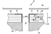
다중-빔릿 사중극자 편향기(1)는 실질적으로 평면형인 기판(3)을 포함하고, 상기 평면형 기판(3)은 행들(rows) 및 열들로 규칙적으로 배열된 관통 개구부들(2)의 어레이를 구비한다. 관통 개구부들(2)은 상기 평면형 기판(3)의 표면(S)에 대해서 실질적으로 횡방향으로 연장하고, 그리고 적어도 하나의 대전 입자 빔릿이 통과하도록 배열된다. The multi-beamlet quadrupole deflector 1 comprises a substantially
평면형 기판(3)의 상단부 상에는, 이러한 예에서 Si 칩이 되는, 전자 제어 회로(4)가 배열된다. 전자 제어 회로(4)는, 관통 개구부들(2)에 인접하여, 특히 평면형 기판(3)의 무비임 지역들 상에 배열된 집적 회로를 포함한다. 상기 전자 제어 회로(4)의 상단부 상에는 절연 층(5)이 제공되고, 상기 절연 층(5)의 상단부 상에, 전극 층(6)이 배열된다. On the upper end of the
상기 관통 개구부들(2)의 각각은, 상기 기판(3) 상에서 관통 개구부들(2) 주위에 배열된 4개의 전극들(7)을 구비한다. 4개의 전극들(7)을 가지는 각각의 관통 개구부(2)가 그러한 관통 개구부(2)를 통해서 횡단하는 하나 이상의 빔릿들을 조작하기 위한 개별적인 조작기(10)를 형성한다. 그에 따라, 조작기 디바이스(1)가, 행들 및 열들로 배열된 개별적인 조작기들(10)의 어레이를 포함한다. Each of the through
바람직하게, 전극들(7)이 몰리브덴으로 제조되나, 그 전극들이 다른 전도성 재료들로 또한 제조될 수 있을 것이다. 전극 층(6)은 약 4 마이크로미터의 두께를 가지고, 그리고 전극들은 반응성 이온 에칭을 이용한 몰리브덴의 이방성 에칭에 의해서 제조된다. Preferably, the
도 2의 개략적인 평면도에 도시된 바와 같이, 4개의 전극들(7)이 전극 층(6)의 나머지 부분(8)에 의해서 둘러싸인다는 것을 알 수 있을 것이다. 전극들(7)로부터 전기적으로 격리되는 이러한 나머지 부분(8)은, 거리를 두고 4개의 전극들(7)을 둘러싸는 접지된 전극(8)으로서 이용된다. 전극 층(6) 아래에, 전극들(7)의 각각을 절연 재료(5)의 층 아래의 전자 제어 회로(4)에 연결하기 위한 비아들(51)을 구비하는 절연 재료(5)의 층이 존재한다. As shown in the schematic plan view of FIG. 2, it will be appreciated that the four
전자 제어 회로(4)는 각각의 관통 개구부(2)의 4개의 전극들(7)의 각각에 대해서 제어 신호들을 제공한다. 전자 제어 회로(4)는 상기 평면형 기판(3) 상에 그리고 적어도 부분적으로 상기 관통 개구부들(2)에 인접하여 배열되고, 그리고 각각의 관통 개구부(2)의 4개의 전극들(7)의 각각으로 하나 이상의 대전 입자 빔릿을 편향시키기 위한 개별적으로 조정가능한 전압을 제공하도록 배열되며, 상기 대전 입자 빔릿은, 사용 중에, 상기 개구부(2)를 통해서 횡단한다. 그에 따라, 상기 편향기(10)에 의해서 유도된 대전 입자 빔릿의 편향의 양을 개별적으로 조정하기 위한 조정가능한 전압을 이용하여, 상기 조작기 디바이스(1)의 각각의 조작기(10)가 평면형 기판(3)의 표면(S)에 평행한 평면을 따른 임의 방향으로 대전 입자 빔릿을 편향시키기 위해서 이용될 수 있다.The electronic control circuit 4 provides control signals for each of the four
도 4 및 5는 발명의 디바이스 내에서 이용하기 위한 조작기(11)의 제 2 예를 도시한다. 본질적으로, 이러한 제 2 예의 조작기 디바이스는 도 2의 분해도에서 도시된 디바이스와 동일한 구조를 가진다. 즉, 도 4의 평면도에서 도시된 바와 같이, 디바이스는 실질적으로 평면형인 기판(13)을 포함하고, 상기 평면형 기판(13)은 행들 및 열들로 규칙적으로 배열된 관통 개구부들(12)의 어레이를 구비한다. 관통 개구부들(12)은 적어도 하나의 대전 입자 빔릿이 통과하도록 배열되고, 그리고 상기 관통 개구부(12)를 둘러싸는 하나의 전극(17)을 구비한다. 4 and 5 show a second example of the
상기 평면형 기판(13)의 상단부 상에는 전자 제어 회로(14)가 배열된다. 전자 제어 회로(14)는, 관통 개구부들(12)에 인접하여 배열된 집적 회로를 포함한다. 이러한 예에서, 상기 전자 제어 회로(14)는, 비아들(51)과 상호 연결된, 집적된 전자 회로망을 이용하여 몇몇 층들(15)로부터 구축된다. The
또한, 관통 개구부들(12)의 엣지에서, 비아들(52)이 제공되고, 그러한 비아들(52)은 상단부 전극(17)에 연결된다. 상기 비아들(52)은 상기 관통 개구부들(12) 내부에서 상단부 전극(17)의 연장부를 제공한다. 그에 따라, 관통 개구부의 전극(17)이 상기 관통 개구부의 내측 대면 벽에 대하여 적어도 부분적으로 배열된다. 관통 개구부들(12)의 엣지에서의 비아들(52)이 집적된 전자 제어 회로(14)의 제조를 위해서 이용되는 프로세스와 동일한 프로세스를 이용하여 그리고 동시에 제조된다.In addition, at the edge of the through
관통 개구부들(12)의 각각이 상기 기판(13) 상에서 관통 개구부들(12) 주위로 배열된 하나의 전극(17)을 구비한다. 상기 평면형인 기판(13) 위의 소정 거리에서, 추가적인 전극(19)이 배열된다. 상기 추가적인 전극(19)은 또한 관통 개구부들(12')의 어레이를 포함하고, 도 5의 횡단면에서 개략적으로 도시된 바와 같이, 상기 관통 개구부들(12')은 기판(13)의 관통 개구부들(12)과 정렬된다. 전극(17) 및 추가적인 전극(19)을 가지는 관통 개구부(12) 각각이 개별적인 아인젤 렌즈(11)를 형성하고, 상기 아인젤 렌즈(11)에는, 사용 중에, 상기 렌즈(11)의 포커스 거리 또는 강도를 개별적으로 조정하기 위한 조정가능 전압이 제공된다. Each of the through
그에 따라, 이러한 제 2 예는 조작기 디바이스(16)를 제공하고, 상기 조작기 디바이스(16)는 정전기 렌즈들(11)의 어레이를 포함하고, 상기 정전기 렌즈들(11)의 각각이 상기 관통 개구부들 중의 하나의 관통 개구부(12)를 포함하고, 상기 관통 개구부들(12)의 각각은 상응하는 관통 개구부(12) 주위로 배열된 하나의 전극(17)을 포함하고, 그리고 상기 전자 제어 회로(14)는, 상기 렌즈(11)의 강도를 개별적으로 조정하기 위한 조정가능 전압을 상기 정전기 렌즈들의 어레이 중의 렌즈(11)의 각각의 개별적인 관통 개구부의 하나의 전극(17)으로 제공하도록 배열된다. Accordingly, this second example provides a
도 6은 발명의 조작기 디바이스(20)의 제 3 예를 도시한다. 본질적으로, 이러한 제 3 의 조작기 디바이스(20)는 도 2의 분해도에 도시된 디바이스와 동일한 구조를 가진다. 즉, 도 6의 평면도에서 도시된 바와 같이, 디바이스가 실질적으로 평면형인 기판을 포함하고, 상기 평면형인 기판은 행들 및 열들로 규칙적으로 배열된 관통 개구부들(22)의 어레이를 구비한다. 관통 개구부들(22)은 적어도 하나의 대전 입자 빔릿이 통과하도록 배열된다. 각각의 관통 개구부(22)는 관통 개구부(12)를 둘러싸는 8개의 전극들(27)을 구비한다. 전극들(17)을 가지는 각각의 관통 개구부(12)가 개별적인 팔중극자 편향기를 형성하고, 사용 중에, 상기 팔중극자 편향기로, 예를 들어, 각각의 개별적인 빔릿에 대한 무수차 교정을 제공하기 위해서, 상기 관통 개구부들(12) 중 하나를 횡단하는 빔릿들의 궤적을 개별적으로 조정하기 위한 조정가능한 전압이 제공된다. 6 shows a third example of the
그에 따라, 이러한 제 3 예의 조작기 디바이스(20)는, 예를 들어 빔릿들의 임의의 비점수차를 교정하기 위한, 정전기 무수차 교정기들(21)을 포함하고, 상기 정전기 무수차 교정기들(21)의 각각이 상기 관통 개구부들의 어레이 중의 하나의 관통 개구부(22)를 포함하고, 상기 관통 개구부들(22)의 각각이 상응하는 관통 개구부(22) 주위로 배열된 8개의 전극들(27)을 포함하고, 그리고 상기 무수차 교정기에 의해서 유도되는 대전 입자 빔릿들의 무수차 교정의 양을 개별적으로 조정하기 위한 조정가능한 전압을 상기 정전기 무수차 교정기들의 어레이 중의 무수차 교정기(21)의 각각의 개별적인 관통 개구부(22)의 8개의 전극들(27)로 제공하도록 상기 전자 제어 회로가 배열된다. Accordingly, this third
발명의 디바이스의 추가적인 예에서, 도 7의 부분적인 횡단면도에서 도시된 바와 같이, 디바이스(31)는, 제 1 평면형인 기판(33)의 평면 내에 관통 개구부들(32)의 제 1 어레이를 포함하는 제 1 평면형인 기판(33)을 가지는 제 1 조작기 디바이스(30)를 포함하고, 상기 관통 개구부들(32)의 각각은 상기 상응하는 관통 개구부(32) 주위에 배열된 하나 이상의 전극들(37)을 포함하고, 그리고 상기 하나 이상의 전극들(37)이 상기 기판(33) 상에 배열된다. 또한, 디바이스(31)는 제 2 평면형 기판의 평면 내에서 관통 개구부들(32')의 제 2 어레이를 포함하는 제 2 평면형인 기판(33')을 가지는 제 2 조작기 디바이스(30')를 포함하고, 상기 관통 개구부들(32')의 각각은 상응하는 관통 개구부(32') 주위에 배열된 하나 이상의 전극들(37')을 포함하고, 그리고 상기 하나 이상의 전극들(37')이 상기 기판(33') 상에 배열된다. 제 2 평면형인 기판(33')은 상기 제 1 평면형 기판(33)에 대해서 거리(d)를 두고 그리고 실질적으로 평행하게 배열되고, 제 2 조작기 디바이스(30')의 각각의 관통 개구부(32')가 상기 제 1 조작기 디바이스(30)의 관통 개구부(32)와 적어도 실질적으로 일직선으로 위치된다. 하나의 실시예에서, 제 1 조작기 디바이스(30) 및 제 2 조작기 디바이스(30')가 하나의 유닛으로 형성된다. In a further example of the device of the invention, as shown in the partial cross-sectional view of FIG. 7, the
관통 개구부들(32, 32')이 반경(r)을 가지고, 그리고 상기 제 1 및 제 2 평면형 기판들 사이의 거리(d)가 적절하게 상기 반경(r)과 같거나 그보다 작다. 또한, 제 1 및 제 2 조작기 디바이스들(30 및 30')의 하나 이상의 전극들(37, 37')이 상기 제 1 및 제 2 기판들(33, 33') 상에 배열되고, 그에 따라, 상기 제 1 기판(33) 상의 하나 이상의 전극들(37) 및 상기 제 2 기판(33') 상의 하나 이상의 전극들(37')이 서로 대면한다. 제 1 조작기 디바이스(30)의 각각의 관통 개구부(32)를 제 2 조작기 디바이스(30')의 상응하는 관통 개구부(32')와 조합하기 위해서, 상기 제 2 조작기 디바이스(30')가 상기 제 1 조작기 디바이스(30)에 대해서, 적어도 상기 제 1 및 제 2 조작기 디바이스들(30, 30') 사이의 중심 평면에 대해서, 실질적으로 거울 대칭이 된다. The through
제 1 조작기 디바이스(30) 및 제 2 조작기 디바이스(30')의 각각이 각각의 관통 개구부(32, 32')에 대해서 둘 이상의 전극들(37, 37')을, 예를 들어 도 2 및 3에 도시된 바와 같이 4개의 전극들을 가지는 편향기들의 어레이, 도 4에 도시된 바와 같이 각각의 관통 개구부(32, 32')를 위한 전극(37, 37')을 가지는 정전기 렌즈들의 어레이, 및/또는 도 6에 도시된 바와 같이 각각이 관통 개구부(32, 32')를 위한 8개의 전극들을 가지는 정전기 무수차 교정기들의 어레이를 포함할 수 있을 것이다. Each of the
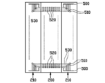
도 1에 도시된 바와 같은 대전 입자 다중-빔릿 리소그래피 디바이스(100)를 다시 참조하면, 빔릿들(122)이 그룹들로 배열된다는 것을 알 수 있을 것이다. 빔릿들(122)의 그룹화로 인해서, 하위-비임들(121)을 생성하기 위해서 시준된 비임(120)의 일부를 차단하는 개구 어레이(104) 이후의 대전 입자 컬럼의 디바이스들이, 도 8a에 개략적으로 도시된 바와 같이, 비임 지역들(200)과 무비임 지역들(210)로 분할될 수 있다. 예를 들어 하위-비임들(121)에 의해서 규정되는 바와 같이, 빔릿들의 그룹들 사이에 위치되는 이들 무비임 지역들(210)은, 도 8b에 개략적으로 도시된 바와 같이, 비임 지역들(200) 내에 배열된 조작기들(520)을 제어하는 전자 제어 회로(510)를 위한 위치로서 이용될 수 있다. 무비임 지역들의 엣지에 근접하여, 커넥터들(500)이 제공되고, 그러한 커넥터들은, 데이터 라인들을 이용하여, 비임 지역(200) 내의 각각의 조작기(520)를 위한 전자 제어 회로들(510)에 연결된다. 각각의 전자 제어 회로들(510)로부터, 전압 라인들이, 개별적인 조정가능한 전압을 각각의 전극으로 제공하기 위해서, 각각의 조작기(520)의 개별적인 전극들로 지향된다. Referring back to the charged particle
무비임 지역들(210)의 위치에서, 비임 지역(200)에 인접하여 배열된 조작기 디바이스들을 위한 제어 데이터를 저장하기 위한 집적된 전자 제어 회로의 메모리 디바이스들을 배열하기 위해서 충분한 공간이 이용될 수 있다. 특히, 메모리들은 각각의 개별적인 조작기(520)를 위한 여러 상이한 레벨들에서 전압을 셋팅하기 위한 제어 데이터를 저장하기 위해서 배열된다. At the location of the
또한, 다중화된 데이터 신호를 역다중화하기 위해서 그리고 역다중화된 데이터를 전자 제어 회로 및/또는 그 메모리 디바이스들로 전달하기 위해서, 역다중화기가 무비임 지역들(210) 내에 배열된다. 그러한 실시예는 무비임 지역(201) 마다 실질적으로 하나의 데이터 리드를 필요로 하고, 이는 연결 리드들의 수를 크게 줄인다. In addition, a demultiplexer is arranged in the
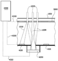
발명들의 추가적인 예시적 실시예가 도 9에 도시되어 있다. 도 9는 개별적인 빔릿들의 비임 성질들을 측정하기 위한 대전 입자 다중-빔릿 검사 장치의 개략적인 횡단면도를 도시한다. 대전 입자 다중-빔릿 검사 장치는, 사용 중에, 빔릿들(1220)의 그룹과 정렬되는 입구 개구 어레이(1050)를 포함하며, 그에 따라 이러한 빔릿들(1220)이 검사 장치로 진입한다. 발명에 따라서, 검사 장치는, 제어기(4300)로부터의 제어 신호(4330)에 따라서 하나 이상의 빔릿들(1220)을 개별적으로 편향시키기 위해서, 예를 들어 도 2, 3 및 6에 도시된 바와 같이, 개별적인 빔릿들 조작기들(2, 22)을 포함하는 조작기 디바이스(3000)를 포함한다. 입구 개구 어레이(1050)로부터 멀어지는 쪽으로 대면하는 조작기 디바이스(3000)로부터의 측부에서 그리고 상기 조작기 디바이스(3000)로부터 거리를 두고, 일련의 센서들(4100, 4101, 4200)이 배열된다. A further exemplary embodiment of the inventions is shown in FIG. 9. 9 shows a schematic cross sectional view of a charged particle multi-beamlet inspection apparatus for measuring beam properties of individual beamlets. The charged particle multi-beamlet inspection apparatus includes, in use, an
이러한 예에서, 일련의 센서들이 패러데이(Faraday) 컵을 포함하는 중앙 센서(4200)를 포함한다. 모든 빔릿들(1220)을 패러데이 컵(4200)으로 편향시키기 위해서 제어기(4300)가 조작기 디바이스(3000)의 개별적인 빔릿 조작기들로 제어 신호들(4330)을 제공할 때, 대전 입자 빔릿들(1220)의 전체 전류가 측정된다. 패러데이 컵(4200)의 측정의 측정 신호(4310)가 제어기(4300)로 지향되고 그리고 디스플레이되고, 저장되고 및/또는 제어기(4300)에서 추가적으로 평가될 수 있다. In this example, the series of sensors includes a
또한, 중앙 센서(4200)가 개별적인 빔릿들(1230)의 비임 성질들을 측정하기 위한 몇 개의 센서들(4100, 4101)에 의해서 둘러싸인다. 개별적인 빔릿(1230)의 비임 성질을 측정하기 위해서, 제어기(4300)는 개별적인 빔릿(1230)을 센서들(4100) 중 하나 상으로 편향시키기 위한 제어 신호(4330)를 제공한다. 조작기 디바이스(3000)가 도 2, 3에 도시된 바와 같이 개별적인 편향기들(2)을 포함하는 경우에, 개별적인 빔릿들(1230)이 임의 방향으로 편향될 수 있고 그리고 특정 방향을 따른 편향량이 개별적으로 조정될 수 있다. 그에 따라, 상이한 비임 성질들을 측정하기 위해서, 각각의 개별적인 빔릿(1230)이 둘 이상의 센서들(4100, 4101)로 순차적으로 지향될 수 있다. 예를 들어, 둘 이상의 센서들(4100, 4101) 중 하나가 개별적인 빔릿(1230)의 전체 전류를 측정하도록 배열되고, 둘 이상의 센서들(4100, 4101) 중의 제 2 센서가, 상기 제 2 센서에 걸쳐서 제 1 방향으로 개별적인 빔릿(1230)이 스캔되는 동안, 제 1 비임 프로파일을 측정하도록 배열되고, 그리고 둘 이상의 센서들(4100, 4101) 중의 제 3 센서가, 상기 제 1 방향에 적어도 실질적으로 수직인 제 2 방향으로 상기 제 3 센서에 걸쳐서 상기 개별적인 빔릿(1230)이 스캔되는 동안, 제 2 비임 프로파일을 측정하도록 배열된다. 센서들(4100, 4101)의 측정의 측정 신호(4320)가 제어기(4300)로 지향될 수 있고, 디스플레이될 수 있고, 및/또는 제어기(4300) 내에서 추가적으로 평가될 수 있다. In addition, the
전술한 설명은 바람직한 실시예들의 동작을 설명하기 위해서 포함된 것이고 발명의 범위를 제한하는 것을 의미하지 않는다는 것을 이해할 수 있을 것이다. 전술한 설명으로부터, 당업자는 본원 발명의 사상 및 범주에 여전히 포함될 수 있는 많은 변경들을 명확하게 인지할 수 있을 것이다. It is to be understood that the foregoing description is included for the purpose of describing the operation of the preferred embodiments and is not meant to limit the scope of the invention. From the foregoing description, those skilled in the art will clearly recognize many changes that may still be included in the spirit and scope of the invention.
요약하면, 본원 발명은 대전 입자 다중-빔릿 장치에서 복수의 대전 입자 빔릿들 중의 하나 이상의 대전 입자 비임들의 조작을 위한 방법 및 장치에 관한 것이다. 조작기 디바이스는 기판의 평면 내의 관통 개구부들의 어레이를 포함하는 평면형 기판으로서, 상기 관통 개구부들의 각각은 하나 이상의 대전 입자 빔릿의 통과를 위해서 배열되고, 상기 관통 개구부들의 각각이 상기 관통 개구부 주위에 배열된 하나 이상의 전극들을 구비하는, 평면형 기판, 그리고 상기 각각의 관통 개구부의 하나 이상의 전극들로 제어 신호들을 제공하기 위한 전자 제어 회로를 포함하며, 전자 제어 회로는 적어도 실질적으로 아날로그 조정가능한 전압을 상기 각각의 개별적인 관통 개구부의 하나 이상의 전극들로 제공하도록 배열된다. In summary, the present invention relates to a method and apparatus for the manipulation of one or more charged particle beams of a plurality of charged particle beamlets in a charged particle multi-beamlet apparatus. The manipulator device is a planar substrate comprising an array of through openings in the plane of the substrate, each of the through openings arranged for passage of one or more charged particle beamlets, one each of the through openings arranged around the through opening. A planar substrate having one or more electrodes, and an electronic control circuit for providing control signals to one or more electrodes of each of the through openings, wherein the electronic control circuit comprises at least substantially analog adjustable voltages to each of the respective individual electrodes. And to provide one or more electrodes of the through opening.
본 발명에 따른 일 실시예는, 대전 입자 다중 빔릿 장치 내에서 하나 이상의 대전 입자 빔릿들의 궤적을 좌우하기 위한 및/또는 제어하기 위한 방법으로서, 상기 대전 입자 다중 빔릿 장치는 대전 입자 공급원을 이용하여 확장하는 대전 입자 비임을 생성하기 위해서, 시준기를 이용하여 대전 입자 비임을 시준하기 위해서, 개구 어레이를 이용하여 타겟을 노광하기 위한 다중 빔릿들을 생성하기 위해서, 빔릿 블랭커 어레이(beamlet blander array)를 이용하여 빔릿들의 그룹 내의 개별적인 빔릿들을 블랭크(blank)하기 위해서, 빔릿들의 그룹 내의 개별적인 빔릿들을 특정 시기에 편향시키기 위해서, 비임 중단부 어레이를 이용하여 편향된 개별적인 빔릿들을 중단시키기 위해서, 그리고 투사 렌즈 시스템을 이용하여 중단되지 않은 빔릿들을 타겟 상으로 투사하기 위해서 광학 컬럼을 포함하고, 다중 빔릿 각각은 빔릿 블랭커 어레이에 의해 블랭크되지 않는 경우에 타겟을 노광하며, 상기 대전 입자 다중 빔릿 장치는 이 장치 내에서 복수의 대전 입자 빔릿 중 하나 이상의 대전 입자 비임들의 조작을 위한 조작기 디바이스를 포함하고, 상기 조작기 디바이스는 빔릿 블랭커 어레이와 빔 중단부 어레이 사이에 배치되며, 상기 조작기 디바이스는 기판의 평면 내의 관통 개구부들의 어레이를 포함하는 평면형 기판으로서, 관통 개구부들의 각각은 하나 이상의 대전 입자 빔릿을 통과시키도록 배치되고, 관통 개구부들의 각각에는 관통 개구부 주위로 배치된 하나 이상의 전극들이 마련되고, 하나 이상의 전극들이 상기 기판 내에 및/또는 기판 상에 배치되는, 평면형 기판과, 관통 개구부들의 어레이의 각각의 관통 개구부의 하나 이상의 전극들로 제어 신호들을 제공하기 위한 전자 제어 회로를 포함하며, 상기 방법은 적어도 실질적으로 아날로그 조정 가능한 전압을 각각의 개별적인 관통 개구부의 하나 이상의 전극들에 제공함으로써 각각의 관통 개구부에 대한 개별적인 조정 제어를 제공하는 단계를 포함하고, 상기 대전 입자 다중 빔릿 장치는 입사하는 상기 대전 입자 빔릿들의 적어도 하나의 특성을 측정하기 위한 센서를 포함하고, 상기 센서는 상기 전자 제어 회로에 연결되며, 상기 센서는, 빔릿들이 블랭크될 때에 지향되는 위치 또는 처리 완료된 타겟과 처리 대상 타겟의 교환 중에 타겟의 위치에 마련되고, 상기 방법은, 하나 이상의 개별적인 빔릿의 악화 및/또는 드리프트를 적어도 실질적으로 교정하도록 조작기 디바이스에 대한 교정된 셋팅들을 제공하기 위해, 센서에 의해 전자 제어 회로에 제공되는 피드백 신호에 기초하여, 각각의 조정 가능한 전압을 각각의 빔릿의 원하는 교정을 얻기 위한 값으로 셋팅하는 것에 의해 각각의 관통 개구부에 대한 상기 개별적인 조정 제어를 제공하는 단계를 포함한다. One embodiment according to the present invention is a method for controlling and / or controlling the trajectory of one or more charged particle beamlets in a charged particle multi-beamlet device, wherein the charged particle multi-beamlet device is extended using a charged particle source. In order to generate a charged particle beam, to collimate a charged particle beam using a collimator, to generate multiple beamlets for exposing a target using an aperture array, a beamlet blanker array is used. To blank individual beamlets in a group of beamlets, to deflect individual beamlets in a group of beamlets at a specific time, to stop individual beamlets deflected using a beam stop array, and using a projection lens system. Project uninterrupted beamlets onto the target Optical beams, each of the multiple beamlets each exposing a target if it is not blanked by the beamlet blanker array, wherein the charged particle multi-beamlet device is configured to A manipulator device for manipulation, wherein the manipulator device is disposed between the beamlet blanker array and the beam stop array, the manipulator device comprising a array of through openings in the plane of the substrate, each of the through openings. Is arranged to pass through one or more charged particle beamlets, each of the through openings is provided with one or more electrodes disposed around the through opening, and the one or more electrodes are disposed in and / or on the substrate; Each through dog of the array of through openings An electronic control circuit for providing control signals to the negative one or more electrodes, wherein the method provides at least a substantially analog adjustable voltage to the one or more electrodes of each individual through opening, thereby providing a separate for each through opening. Providing adjustment control, wherein the charged particle multi-beamlet device comprises a sensor for measuring at least one characteristic of the charged particle beamlets that are incident, the sensor connected to the electronic control circuit, the sensor Is provided at a position that is directed when the beamlets are blanked or at a position of the target during the exchange of the processed target and the processed target, wherein the method includes at least substantially manipulating the deterioration and / or drift of one or more individual beamlets. Providing calibrated settings for To provide said individual adjustment control for each through opening by setting each adjustable voltage to a value to obtain a desired calibration of each beamlet, based on a feedback signal provided to the electronic control circuit by the sensor. It includes a step.
상기 조작기 디바이스는 정전 렌즈(electrostatic lens)들의 어레이를 포함하고, 상기 정전 렌즈들의 각각은 상기 관통 개구부들의 어레이 중의 하나의 관통 개구부를 포함하며, 상기 관통 개구부들의 각각이 상응하는 관통 개구부 주위에 배치된 하나의 전극을 포함하고, 상기 전자 제어 회로는, 상기 정전 렌즈들의 어레이 중의 렌즈의 각각의 개별적인 관통 개구부의 하나의 전극으로 적어도 실질적으로 아날로그 조정 가능한 전압을 제공함으로써, 상기 정전 렌즈들의 각각의 강도를 개별적으로 조정하도록 구성될 수 있다. The manipulator device includes an array of electrostatic lenses, each of the electrostatic lenses comprising a through opening of one of the array of through openings, each of the through openings disposed around a corresponding through opening. And one electrode, wherein the electronic control circuit provides at least substantially analog adjustable voltage to one electrode of each individual through opening of the lens in the array of electrostatic lenses, thereby increasing the intensity of each of the electrostatic lenses. It can be configured to adjust individually.
상기 조작기 디바이스가 정전 편향기들의 어레이를 포함하고, 상기 정전 편향기들의 각각이 상기 관통 개구부들의 어레이 중의 하나의 관통 개구부를 포함하며, 상기 관통 개구부들의 각각이 상응하는 관통 개구부 주위에 배치된 둘 이상의 전극들을 포함하고, 상기 전자 제어 회로는, 상기 정전 편향기들의 어레이 중의 편향기의 각각의 개별적인 관통 개구부의 둘 이상의 전극들에 적어도 실질적으로 아날로그 조정 가능한 전압을 제공함으로써, 상기 편향기에 의해서 유도된 대전 입자 빔릿의 편향의 양을 개별적으로 조정하도록 구성될 수 있다. The manipulator device comprises an array of electrostatic deflectors, each of the electrostatic deflectors including a through opening of one of the array of through openings, each of the two or more of the through openings disposed around a corresponding through opening And electrodes, wherein the electronic control circuit is configured to provide at least substantially analog adjustable voltages to at least two electrodes of each respective through opening of the deflector in the array of electrostatic deflectors, thereby providing charging induced by the deflector. It can be configured to individually adjust the amount of deflection of the particle beamlet.
상기 조작기 디바이스는 정전 비점수차(astigmatism) 교정기들의 어레이를 포함하고, 상기 정전 비점수차 교정기들의 각각이 상기 관통 개구부들의 어레이 중의 하나의 관통 개구부를 포함하며, 상기 관통 개구부들의 각각이 상응하는 관통 개구부 주위에 배치된 8개의 전극들을 포함하고, 상기 전자 제어 회로는, 상기 정전 비점수차 교정기들의 어레이 중의 비점수차 교정기의 각각의 개별적인 관통 개구부의 8개의 전극들에 적어도 실질적으로 아날로그 조정 가능한 전압을 제공함으로써, 상기 비점수차 교정기에 의해서 유도된 대전 입자 빔릿의 비점수차의 교정량을 개별적으로 조정하도록 구성될 수 있다.The manipulator device includes an array of electrostatic astigmatism correctors, each of the electrostatic astigmatism correctors including a through opening of one of the array of through openings, each of the through openings surrounding a corresponding through opening. Wherein the electronic control circuit provides at least substantially analog adjustable voltages to the eight electrodes of each individual through opening of the astigmatism corrector in the array of electrostatic astigmatism correctors, It can be configured to individually adjust the amount of correction of the astigmatism of the charged particle beamlet induced by the astigmatism corrector.
상기 조작기 디바이스는 - 대전 입자 광학 컬럼의 하나 이상의 디바이스들의 오정렬을 교정하기 위해서 상기 대전 입자 광학 컬럼의 광학 축에 실질적으로 수직한 평면 내에서 상기 하나 이상의 대전 입자 빔릿들 중 하나 이상을 편향시키기 위해서, 및/또는 - 비점수차에 대해서 상기 하나 이상의 대전 입자 빔릿들 중 하나 이상을 교정하기 위해서 배치될 수 있다.The manipulator device is adapted to deflect one or more of the one or more charged particle beamlets in a plane substantially perpendicular to the optical axis of the charged particle optical column to correct misalignment of one or more devices of the charged particle optical column, And / or-calibrate one or more of the one or more charged particle beamlets for astigmatism.
본 발명에 따른 일 실시예에서, 대전 입자 다중 빔릿 장치 내에서 하나 이상의 대전 입자 빔릿들의 궤적을 좌우하기 위한 및/또는 제어하기 위한 방법으로서, 대전 입자 다중 빔릿 장치는 대전 입자 공급원을 이용하여 확장하는 대전 입자 비임을 생성하기 위해서, 시준기를 이용하여 상기 대전 입자 비임을 시준하기 위해서, 개구 어레이를 이용하여 타겟을 노광하기 위한 다중 빔릿들을 생성하기 위해서, 빔릿 블랭커 어레이를 이용하여 빔릿들의 그룹 내의 개별적인 빔릿들을 블랭크(blank)하기 위해서, 빔릿들의 그룹 내의 개별적인 빔릿들을 편향시키기 위해서, 비임 중단부 어레이를 이용하여 편향된 개별적인빔릿들을 중단시키기 위해서, 그리고 투사 렌즈 시스템을 이용하여 중단되지 않은 빔릿들을 타겟 상으로 투사하기 위해서 광학 컬럼을 포함하고, 다중 빔릿 각각은 빔릿 블랭커 어레이에 의해 블랭크되지 않는 경우에 타겟을 노광하며, 상기 대전 입자 다중 빔릿 장치는 이 장치 내에서 복수의 대전 입자 빔릿 중 하나 이상의 대전 입자 비임들의 조작을 위한 조작기 디바이스를 포함하고, 상기 조작기 디바이스는 투사 렌즈 시스템에서 상기 하나 이상의 대전 입자 빔릿들 중 하나 이상의 편향 및/또는 포커싱이나 디포커싱을 제공하기 위해 투사 렌즈 시스템의 부분으로서 마련되며, 상기 조작기 디바이스는 대전 입자 공급원으로부터 멀어지는 방향을 향하는 비임 중단부 어레이의 측부에 배치되고, 상기 조작기 디바이스는 기판의 평면 내의 관통 개구부들의 어레이를 포함하는 평면형 기판으로서, 관통 개구부들의 각각은 하나 이상의 대전 입자 빔릿을 통과시키도록 배치되고, 관통 개구부들의 각각에는 관통 개구부 주위로 배치된 하나 이상의 전극들이 마련되고, 하나 이상의 전극들이 상기 기판 내에 및/또는 기판 상에 배치되는, 평면형 기판과, 관통 개구부들의 어레이의 각각의 관통 개구부의 하나 이상의 전극들로 제어 신호들을 제공하기 위한 전자 제어 회로를 포함하며, 상기 방법은 적어도 실질적으로 아날로그 조정 가능한 전압을 각각의 개별적인 관통 개구부의 하나 이상의 전극들에 제공함으로써 각각의 관통 개구부에 대한 개별적인 조정 제어를 제공하는 단계를 포함하고, 상기 대전 입자 다중 빔릿 장치는 입사하는 상기 대전 입자 빔릿들의 적어도 하나의 특성을 측정하기 위한 센서를 포함하고, 상기 센서는 상기 전자 제어 회로에 연결되며, 상기 센서는, 빔릿들이 블랭크될 때에 지향되는 위치 또는 처리 완료된 타겟과 처리 대상 타겟의 교환 중에 타겟의 위치에 마련되고, 상기 방법은, 하나 이상의 개별적인 빔릿의 악화 및/또는 드리프트를 적어도 실질적으로 교정하도록 조작기 디바이스에 대한 교정된 셋팅들을 제공하기 위해, 센서에 의해 전자 제어 회로에 제공되는 피드백 신호에 기초하여, 각각의 조정 가능한 전압을 각각의 빔릿의 원하는 교정을 얻기 위한 값으로 셋팅하는 것에 의해 각각의 관통 개구부에 대한 상기 개별적인 조정 제어를 제공하는 단계를 포함한다. In one embodiment according to the present invention, a method for controlling and / or controlling the trajectory of one or more charged particle beamlets in a charged particle multi-beamlet apparatus, wherein the charged particle multi-beamlet apparatus extends using a charged particle source. In order to generate a charged particle beam, to collimate the charged particle beam with a collimator, to generate multiple beamlets for exposing a target using an array of apertures, a beamlet blanker array is used to separate individual within a group of beamlets. To blank beamlets, to deflect individual beamlets within a group of beamlets, to stop individual beamlets deflected using a beam interrupt array, and to use unprojected beamlets onto a target using a projection lens system. Including an optical column to project And each of the multiple beamlets exposes a target when it is not blanked by the beamlet blanker array, wherein the charged particle multi-beamlet device is a manipulator device for manipulation of one or more charged particle beams of the plurality of charged particle beamlets within the apparatus. Wherein the manipulator device is provided as part of the projection lens system to provide deflection and / or focusing or defocusing one or more of the one or more charged particle beamlets in the projection lens system, the manipulator device being a source of charged particles. Disposed on the side of the beam stop array facing away from the manipulator device, wherein the manipulator device is a planar substrate comprising an array of through openings in the plane of the substrate, each of the through openings being arranged to pass through one or more charged particle beamlets; Through openings Each provided with one or more electrodes disposed around the through opening, wherein the one or more electrodes are disposed in and / or on the substrate and to one or more electrodes of each through opening of the array of through openings. An electronic control circuit for providing control signals, the method providing individual adjustment control for each through opening by providing at least substantially analog adjustable voltages to one or more electrodes of each respective through opening. Wherein the charged particle multi-beamlet device comprises a sensor for measuring at least one characteristic of the charged particle beamlets that are incident, the sensor connected to the electronic control circuit, wherein the sensor is configured to blank the beamlets. Position or processed target and processing Provided at the location of the target during exchange of the target target, the method further comprising electronic control circuitry by the sensor to provide calibrated settings for the manipulator device to at least substantially correct deterioration and / or drift of one or more individual beamlets And based on the feedback signal provided at, providing the respective adjustment control for each through opening by setting each adjustable voltage to a value to obtain a desired calibration of each beamlet.
본 발명에 따른 일 실시예는, 광학 컬럼을 포함하는 대전 입자 다중 빔릿 장치로서, 확장하는 대전 입자 비임을 생성하는 대전 입자 공급원, 대전 입자 비임을 시준하는 시준기 렌즈, 타겟을 노광하기 위한 다중 빔릿들을 생성하는 개구 어레이, 빔릿들의 그룹 내의 개별적인 빔릿들을 특정 시기에 편향시켜 블랭크하는 빔릿 블랭커 어레이, 편향된 개별적인 빔릿들을 중단하는 빔 중단부 어레이, 및 중단되지 않은 빔릿을 타겟으로 투사하는 투사 렌즈 시스템을 포함하고 다중 빔릿 각각은 빔릿 블랭커 어레이에 의해 블랭크되지 않는 경우에 타겟을 노광하며, 상기 대전 입자 다중 빔릿 장치는 이 대전 입자 다중 빔릿 장치 내에서 복수의 대전 입자 빔릿 중 하나 이상의 대전 입자 비임들의 조작을 위한 조작기 디바이스를 포함하고, 상기 조작기 디바이스는 빔릿 블랭커 어레이와 빔 중단부 어레이 사이에 배치되며, 상기 조작기 디바이스는 기판의 평면 내의 관통 개구부들의 어레이를 포함하는 평면형 기판으로서, 관통 개구부들의 각각은 하나 이상의 대전 입자 빔릿을 통과시키도록 배치되고, 관통 개구부들의 각각에는 관통 개구부 주위로 배치된 하나 이상의 전극들이 마련되고, 하나 이상의 전극들이 상기 기판 내에 및/또는 기판 상에 배치되는, 평면형 기판과, 각각의 관통 개구부의 하나 이상의 전극들에 제어 신호를 제공하는 전자 제어 회로를 포함하며, 상기 전자 제어 회로는 적어도 실질적으로 아날로그 조정 가능한 전압을 각각의 개별적인 관통 개구부의 하나 이상의 전극들에 제공하도록 구성되고, 상기 대전 입자 다중 빔릿 장치는 입사하는 상기 대전 입자 빔릿들의 적어도 하나의 특성을 측정하는 센서를 더 포함하고, 상기 센서는, 센서에 의해 전자 제어 회로에 제공되는 피드백 신호에 기초하여, 각각의 관통 개구부의 개별적인 조정 제어를 제공하도록 상기 전자 제어 회로에 연결되며, 상기 센서는, 빔릿들이 블랭크될 때에 지향되는 위치 또는 처리 완료된 타겟과 처리 대상 타겟의 교환 중에 타겟의 위치에 마련되는 것인 대전 입자 다중 빔릿 장치를 포함한다. An embodiment according to the present invention is a charged particle multi-beamlet device comprising an optical column, comprising: a charged particle source generating an expanding charged particle beam, a collimator lens collimating a charged particle beam, and multiple beamlets for exposing a target; An array of apertures to create, a beamlet blanker array that deflects individual beamlets within a group of beamlets at a specific time and blanks, an array of beam stops to interrupt the deflected individual beamlets, and a projection lens system to project the uninterrupted beamlets to a target And each of the multiple beamlets exposes a target if they are not blanked by the beamlet blanker array, wherein the charged particle multi-beamlet apparatus performs manipulation of one or more charged particle beams of the plurality of charged particle beamlets within the charged particle multi-beamlet apparatus. A manipulator device for said manipulator device Is disposed between the beamlet blanker array and the beam stop array, the manipulator device being a planar substrate comprising an array of through openings in the plane of the substrate, each of the through openings being arranged to pass through one or more charged particle beamlets; Each of the through openings is provided with one or more electrodes disposed around the through opening, the one or more electrodes disposed within and / or on the substrate, the planar substrate and one or more electrodes of each through opening being controlled. An electronic control circuit for providing a signal, wherein the electronic control circuit is configured to provide at least substantially analog adjustable voltage to one or more electrodes of each individual through opening, wherein the charged particle multi-beamlet device is configured to receive the incident At least one characteristic of the charged particle beamlets Further comprising a sensor for measuring, the sensor being connected to the electronic control circuit to provide individual adjustment control of each through opening based on a feedback signal provided by the sensor to the electronic control circuit, wherein the sensor comprises: And a charged particle multiple beamlet device which is provided at a position directed when the beamlets are blanked or at a position of the target during exchange of the processed target and the target to be processed.
전압은 상기 조작기의 각각의 전극에 대해 개별 조정 가능할 수 있다. The voltage may be individually adjustable for each electrode of the manipulator.
상기 조작기 디바이스는, 상기 복수 개의 빔릿의 개별적인 빔릿의 포커싱, 편향 또는 무수차화(stigmation)를 위해 구성될 수 있다. The manipulator device may be configured for focusing, deflection, or stigmation of individual beamlets of the plurality of beamlets.
상기 조작기 디바이스의 평면형 기판은 웨이퍼이고, 상기 전자 제어 회로는 상기 평면형 기판 상에 집적 회로를 포함할 수 있다.The planar substrate of the manipulator device is a wafer, and the electronic control circuit can include an integrated circuit on the planar substrate.
상기 전자 제어 회로는, 적어도 부분적으로, 상기 조작기 디바이스 상의 2개의 관통 개구부들 사이에 배치될 수 있다.The electronic control circuit can be at least partially disposed between two through openings on the manipulator device.
상기 전자 제어 회로는 2개의 관통 개구부들 사이의 또는 상기 조작기 디바이스 상의 관통 개구부들의 2개의 그룹들 사이의 무비임(non-beam) 영역들 내에 배치될 수 있다.The electronic control circuit can be disposed in non-beam regions between two through openings or between two groups of through openings on the manipulator device.
상기 전자 제어 회로는 하나 이상의 개별적인 관통 개구부들의 하나 이상의 전극들에 대한 제어 데이터를 저장하기 위한 메모리를 포함하고, 상기 메모리는 상기 조작기 디바이스의 평면형 기판 상에 그리고 상기 관통 개구부들에 인접하여 배치될 수 있다.The electronic control circuit includes a memory for storing control data for one or more electrodes of one or more individual through openings, the memory may be disposed on the planar substrate of the manipulator device and adjacent the through openings. have.
상기 메모리는 하나의 개별적인 관통 개구부의 하나 이상의 전극들에 대한 제어 데이터를 저장하도록 구성되며, 상기 메모리는 상기 조작기 디바이스의 평면형 기판 상에 그리고 상기 개별적인 관통 개구부에 인접하여 배치될 수 있다.The memory is configured to store control data for one or more electrodes of one individual through opening, the memory may be disposed on the planar substrate of the manipulator device and adjacent to the individual through opening.
상기 메모리는 2개의 관통 개구부들 사이에 배치될 수 있다.The memory may be disposed between two through openings.
상기 조작기 디바이스의 하나 이상의 전극들은 평면형 기판 상에 성막된 금속을 포함할 수 있다.One or more electrodes of the manipulator device may comprise a metal deposited on a planar substrate.
상기 금속은 몰리브덴을 포함할 수 있다.The metal may comprise molybdenum.
상기 조작기 디바이스 내의 관통 개구부의 하나 이상의 전극은 상기 관통 개구부의 내측 대면 벽에 대하여 적어도 부분적으로 배치될 수 있다.One or more electrodes of the through opening in the manipulator device may be at least partially disposed with respect to the inner facing wall of the through opening.
상기 하나 이상의 전극들은 상기 관통 개구부의 중심선에 실질적으로 평행한 방향으로 상기 관통 개구부 내로 연장할 수 있다.The one or more electrodes may extend into the through opening in a direction substantially parallel to a centerline of the through opening.
상기 조작기 디바이스에 있는 각각의 관통 개구부의 하나 이상의 전극들은 접지된 전극에 의해서 적어도 실질적으로 둘러싸이고, 상기 접지된 전극은 상기 평면형 기판 상에서 하나 이상의 전극들과 동일한 평면에 배치되고, 하나 이상의 전극들을 거리를 두고 둘러쌀 수 있다.One or more electrodes of each through opening in the manipulator device are at least substantially surrounded by a grounded electrode, wherein the grounded electrode is disposed in the same plane as the one or more electrodes on the planar substrate and distances the one or more electrodes. Can be surrounded by.
상기 접지된 전극은 평면형 기판 상에 성막된 금속을 포함할 수 있다.The grounded electrode may include a metal deposited on a planar substrate.
상기 금속은 몰리브덴을 포함할 수 있다.The metal may comprise molybdenum.
상기 평면형 기판으로부터 멀어지는 방향을 향하는 상기 조작기 디바이스의 하나 이상의 전극들의 표면은 평면형 기판과 상기 평면형 기판으로부터 멀어지는 방향을 향하는 접지된 전극의 표면 사이의 높이에 배치될 수 있다.The surface of one or more electrodes of the manipulator device facing away from the planar substrate may be disposed at a height between the planar substrate and the surface of the grounded electrode facing away from the planar substrate.
상기 조작기 디바이스에 있는 평면형 기판 상의 접지된 전극의 두께는, 평면형 기판 상의 하나 이상의 전극들의 두께보다 두꺼울 수 있다.The thickness of the grounded electrode on the planar substrate in the manipulator device may be thicker than the thickness of one or more electrodes on the planar substrate.
상기 전자 제어 회로는 이 전자 제어 회로를 상기 조작기 디바이스의 하나 이상의 전극들과 연결하기 위한 연결 리드(lead)들을 포함하고, 상기 연결 리드들 중 적어도 하나는 2개의 접지된 전기 전도 층들 사이에 적어도 부분적으로 배치될 수 있다.The electronic control circuit includes connecting leads for connecting the electronic control circuit with one or more electrodes of the manipulator device, at least one of the connecting leads being at least partially between two grounded electrically conductive layers. It can be arranged as.
상기 연결 리드들 중 적어도 하나는 2개의 접지된 리드들 사이에 적어도 부분적으로 배치될 수 있다.At least one of the connection leads may be at least partially disposed between two grounded leads.
상기 전자 제어 회로는 다중화된 신호로부터 하나 이상의 개별적인 관통 개구부들에 대한 제어 데이터를 추출하기 위한 디멀티플렉서(demultiplexer)를 포함하고, 상기 디멀티플렉서는 상기 조작기 디바이스의 평면형 기판 상에 그리고 상기 관통 개구부들에 인접하여 배치될 수 있다.The electronic control circuit includes a demultiplexer for extracting control data for one or more individual through openings from the multiplexed signal, the demultiplexer on and near the planar substrate of the manipulator device. Can be deployed.
상기 디멀티플렉서는 하나의 개별적인 관통 개구부의 하나 이상의 전극들에 대한 제어 데이터를 추출하도록 구성되며, 상기 디멀티플렉서는 상기 조작기 디바이스의 평면형 기판 상에 그리고 상기 개별적인 관통 개구부에 인접하여 배치될 수 있다.The demultiplexer is configured to extract control data for one or more electrodes of one individual through opening, wherein the demultiplexer may be disposed on a planar substrate of the manipulator device and adjacent to the individual through opening.
상기 디멀티플렉서는 인접한 관통 개구부들 사이에 배치될 수 있다.The demultiplexer may be disposed between adjacent through openings.
상기 조작기 디바이스에 대한 연결 리드들의 개수가 전극들의 개수보다 적을 수 있다. The number of connection leads to the manipulator device may be less than the number of electrodes.
상기 조작기 디바이스의 관통 개구부에 대한 연결 리드들의 개수가 상기 관통 개구부의 전극들의 개수보다 적을 수 있다.The number of connecting leads to the through opening of the manipulator device may be less than the number of the electrodes of the through opening.
상기 조작기 디바이스는, 제 1 평면형 기판의 평면 내에 관통 개구부들의 제 1 어레이를 포함하는 제 1 평면형 기판을 가지는 제 1 조작기 디바이스이고, 상기 대전 입자 다중 빔릿 장치는, 제 2 평면형 기판의 평면 내에 관통 개구부들의 제 2 어레이를 포함하는 제 2 평면형 기판을 가지는 제 2 조작기 디바이스를 포함하며, 상기 관통 개구부들의 각각은 상응하는 관통 개구부 주위에 배치된 하나 이상의 전극들을 포함하고, 상기 하나 이상의 전극들은 상기 기판 내에 및/또는 상기 기판 상에 배치되며, 상기 제 2 평면형 기판은 제 1 평면형 기판에 대해서 거리를 두고 그리고 실질적으로 평행하게 배치되고, 상기 관통 개구부들의 제 2 어레이의 각각의 관통 개구부는 관통 개구부들의 제 1 어레이의 관통 개구부와 적어도 실질적으로 일직선이 될 수 있다.The manipulator device is a first manipulator device having a first planar substrate comprising a first array of through openings in the plane of the first planar substrate, wherein the charged particle multi-beamlet device is a through opening in the plane of the second planar substrate. And a second manipulator device having a second planar substrate comprising a second array of cavities, each of the through openings comprising one or more electrodes disposed around a corresponding through opening, the one or more electrodes within the substrate. And / or disposed on the substrate, wherein the second planar substrate is disposed at a distance and substantially parallel to the first planar substrate, wherein each through opening of the second array of through openings is formed of the through openings; It may be at least substantially straight with the through opening of one array.
상기 관통 개구부들의 제2 어레이의 관통 개구부들은 반경(r)을 가지고, 상기 제 1 평면형 기판과 및 제 2 평면형 기판 사이의 거리(d)는 상기 반경(r) 이하일 수 있다.The through openings of the second array of through openings have a radius r, and the distance d between the first planar substrate and the second planar substrate may be less than or equal to the radius r.
상기 제 1 및 제 2 조작기 디바이스의 하나 이상의 전극들은 상기 제 1 및 제 2 평면형 기판 상에 각각 배치되고, 상기 제 1 평면형 기판 상의 하나 이상의 전극들 및 상기 제 2 평면형 기판 상의 하나 이상의 전극들은 서로 대면할 수 있다.One or more electrodes of the first and second manipulator devices are respectively disposed on the first and second planar substrates, and one or more electrodes on the first planar substrate and one or more electrodes on the second planar substrate face each other. can do.
상기 제 2 조작기 디바이스는 적어도 제 1 조작기 디바이스와 제 2 조작기 디바이스 사이의 중심 평면에 관하여 제 1 조작기 디바이스에 대해 실질적으로 거울 대칭일 수 있다.The second manipulator device may be substantially mirror symmetric with respect to the first manipulator device with respect to the central plane between at least the first manipulator device and the second manipulator device.
상기 센서는 비임 블랭커 어레이를 향하는 빔 중단부 어레이의 측부에 배치될 수 있다.The sensor may be disposed on the side of the beam stop array facing the beam blanker array.
상기 센서는 비임 블랭커 어레이를 향하는 빔 중단부 어레이의 측부에 배치될 수 있다.The sensor may be disposed on the side of the beam stop array facing the beam blanker array.
상기 센서는, 빔 중단부 어레이 상에서 빔릿들이 블랭크될 때에 빔릿 블랭커 어레이에 의해 지향되는 위치에 배치될 수 있다.The sensor may be placed in a position directed by the beamlet blanker array when the beamlets are blanked on the beam stop array.
상기 센서는, 빔 중단부 어레이 상에서 빔릿들이 블랭크될 때에 빔릿 블랭커 어레이에 의해 지향되는 위치에 배치될 수 있다.The sensor may be placed in a position directed by the beamlet blanker array when the beamlets are blanked on the beam stop array.
본 발명에 따른 일 실시예에서, 광학 컬럼을 포함하는 대전 입자 다중 빔릿 무마스크 리소그래피 디바이스로서, 확장하는 대전 입자 비임을 생성하는 대전 입자 공급원, 대전 입자 비임을 시준하는 시준기 렌즈, 타겟을 노광하기 위한 다중 빔릿들을 생성하는 개구 어레이, 빔릿들의 그룹 내의 개별적인 빔릿들을 특정 시기에 편향시켜 블랭크하는 빔릿 블랭커 어레이, 편향된 개별적인 빔릿들을 중단하는 빔 중단부 어레이, 및 중단되지 않은 빔릿들을 타겟으로 투사하는 투사 렌즈 시스템을 포함하고, 다중 빔릿 각각은 빔릿 블랭커 어레이에 의해 블랭크되지 않는 경우에 타겟을 노광하며, 상기 대전 입자 다중 빔릿 무마스크 리소그래피 디바이스는 이 다중 빔릿 무마스크 리소그래피 디바이스 내에서 복수의 대전 입자 빔릿들 중 하나 이상의 대전 입자 비임들의 조작을 위한 조작기 디바이스를 포함하고, 상기 조작기 디바이스는 기판의 평면 내의 관통 개구부들의 어레이를 포함하는 평면형 기판으로서, 관통 개구부들의 각각은 하나 이상의 대전 입자 빔릿을 통과시키도록 배치되고, 관통 개구부들의 각각에는 관통 개구부 주위로 배치된 하나 이상의 전극들이 마련되고, 하나 이상의 전극들이 상기 기판 내에 및/또는 기판 상에 배치되는, 평면형 기판과, 각각의 관통 개구부의 하나 이상의 전극들에 제어 신호를 제공하는 전자 제어 회로를 포함하며, 전자 제어 회로는 적어도 실질적으로 아날로그 조정 가능한 전압을 각각의 개별적인 관통 개구부의 하나 이상의 전극들에 제공하도록 구성되고, 상기 대전 입자 다중 빔릿 무마스크 리소그래피 디바이스는 입사하는 상기 대전 입자 빔릿들의 적어도 하나의 특성을 측정하는 센서를 더 포함하고, 상기 센서는, 센서에 의해 전자 제어 회로에 제공되는 피드백 신호에 기초하여, 각각의 관통 개구부의 개별적인 조정 제어를 제공하도록 상기 전자 제어 회로에 연결되며, 상기 센서는, 빔릿들이 블랭크될 때에 지향되는 위치 또는 처리 완료된 타겟과 처리 대상 타겟의 교환 중에 타겟의 위치에 마련되고, 상기 조작기 디바이스는 투사 렌즈 시스템에서 상기 하나 이상의 대전 입자 빔릿들 중 하나 이상의 편향 및/또는 포커싱이나 디포커싱을 제공하기 위해 투사 렌즈 시스템의 부분으로서 마련되며, 상기 조작기 디바이스는 대전 입자 공급원으로부터 멀어지는 방향을 향하는 비임 중단부 어레이의 측부에 배치되는 것인 대전 입자 다중 빔릿 무마스크 리소그래피 디바이스를 포함한다.In one embodiment according to the invention, a charged particle multi-beamlet maskless lithography device comprising an optical column, comprising: a charged particle source generating an expanding charged particle beam, a collimator lens collimating a charged particle beam, a target for exposing a target An aperture array that generates multiple beamlets, a beamlet blanker array that blanks individual beamlets within a group of beamlets at a specific time, a beam interrupter array that interrupts the deflected individual beamlets, and a projection lens that projects uninterrupted beamlets to the target A system, wherein each of the multiple beamlets exposes a target when it is not blanked by the beamlet blanker array, wherein the charged particle multi-beamlet maskless lithography device comprises a plurality of charged particle beamlets within the multi-beamlet maskless lithography device. One or more of the Great War mouths A manipulator device for manipulation of the beams, the manipulator device comprising a array of through openings in the plane of the substrate, each of the through openings being arranged to pass through one or more charged particle beamlets, Each is provided with one or more electrodes disposed around the through opening, wherein the one or more electrodes are disposed in and / or on the substrate, providing a control signal to the planar substrate and one or more electrodes of each through opening. An electronic control circuit, the electronic control circuit configured to provide at least substantially an analog adjustable voltage to one or more electrodes of each respective through opening, wherein the charged particle multi-beamlet maskless lithographic device is incident to the charged particle At least one of the beamlets And further comprising a sensor for measuring a characteristic of the device, wherein the sensor is connected to the electronic control circuit to provide individual adjustment control of each through opening based on a feedback signal provided by the sensor to the electronic control circuit. The sensor is provided at a position that is directed when the beamlets are blanked or at a position of the target during the exchange of the processed target and the processed target, wherein the manipulator device is configured to deflect one or more of the one or more charged particle beamlets in the projection lens system; Or as part of a projection lens system to provide focusing or defocusing, wherein the manipulator device is disposed on the side of the beam interruption array facing away from the charged particle source. Include.
Claims (9)
확장하는 대전 입자 비임을 생성하는 대전 입자 공급원,
대전 입자 비임을 시준하는 시준기 렌즈,
타겟을 노광하기 위한 다중 빔릿들을 생성하는 개구 어레이,
빔릿들의 그룹 내의 개별적인 빔릿들을 특정 시기에 편향시켜 블랭크하는 빔릿 블랭커 어레이,
편향된 개별적인 빔릿들을 중단하는 빔 중단부 어레이, 및
중단되지 않은 빔릿을 타겟으로 투사하는 투사 렌즈 시스템
을 포함하고
다중 빔릿 각각은 빔릿 블랭커 어레이에 의해 블랭크되지 않는 경우에 타겟을 노광하며,
상기 대전 입자 다중 빔릿 장치는 이 대전 입자 다중 빔릿 장치 내에서 복수의 대전 입자 빔릿 중 하나 이상의 대전 입자 비임들의 조작을 위한 조작기 디바이스를 포함하고,
상기 조작기 디바이스는
평면형 기판의 평면의 관통 개구부들의 어레이를 포함하는 상기 평면형 기판으로서, 관통 개구부들의 각각은 하나 이상의 대전 입자 빔릿을 통과시키도록 배치되고, 관통 개구부들의 각각은 관통 개구부 주위로 배치된 다수의 전극들을 구비하고, 다수의 전극들이 상기 기판 내에 또는 기판 상의 평면형 전극 층에 배치되는, 평면형 기판과,
각각의 관통 개구부의 다수의 전극들에 제어 신호를 제공하는 전자 제어 회로
를 포함하며, 상기 전자 제어 회로는 전압을 각각의 개별적인 관통 개구부의 다수의 전극들에 제공하도록 구성됨으로써, 상기 각각의 개별적인 관통 개구부는 사중극자 편향기 또는 팔중극자 편향기를 포함하며,
상기 평면형 기판은 웨이퍼이고, 상기 전자 제어 회로는 상기 평면형 기판 상에 집적 회로를 포함하는 것인, 대전 입자 다중 빔릿 장치.A charged particle multiple beamlet device comprising an optical column,
A charged particle source generating an expanding charged particle beam,
Collimator lens for collimating charged particle beams,
An aperture array that generates multiple beamlets for exposing a target,
A beamlet blanker array that deflects and blanks individual beamlets in a group of beamlets at a specific time,
A beam stop array for stopping the deflected individual beamlets, and
Projection lens system to project uninterrupted beamlets to the target
Including
Each of the multiple beamlets exposes a target when it is not blanked by the beamlet blanker array,
The charged particle multi-beamlet apparatus includes a manipulator device for manipulation of one or more charged particle beams of the plurality of charged particle beamlets in the charged particle multi-beamlet apparatus,
The manipulator device
Wherein said planar substrate comprises an array of planar through openings of said planar substrate, each of said through openings being arranged to pass through one or more charged particle beamlets, each of said through openings having a plurality of electrodes disposed about said through opening. A planar substrate, the plurality of electrodes disposed in or on the planar electrode layer on the substrate,
Electronic control circuit providing control signals to the plurality of electrodes in each through opening
Wherein the electronic control circuit is configured to provide a voltage to the plurality of electrodes of each individual through opening, such that each individual through opening comprises a quadrupole deflector or an octapole deflector,
Wherein the planar substrate is a wafer and the electronic control circuit comprises an integrated circuit on the planar substrate.
대전 입자 공급원을 이용하여 확장하는 대전 입자 비임을 생성하기 위해서,
시준기를 이용하여 대전 입자 비임을 시준하기 위해서,
타겟을 노광하기 위한 다중 빔릿들을 생성하는 개구 어레이를 이용하기 위해서,
빔릿 블랭커 어레이(beamlet blander array)를 이용하여 빔릿들의 그룹 내의 개별적인 빔릿들을 블랭크(blank)하기 위해서, 빔릿들의 그룹 내의 개별적인 빔릿들을 특정 시기에 편향시키기 위해서,
비임 중단부 어레이를 이용하여 편향된 개별적인 빔릿들을 중단시키기 위해서, 그리고
투사 렌즈 시스템을 이용하여 중단되지 않은 빔릿들을 타겟 상으로 투사하기 위해서
광학 컬럼을 포함하고,
다중 빔릿 각각은 빔릿 블랭커 어레이에 의해 블랭크되지 않는 경우에 타겟을 노광하며,
상기 방법은, 전압을 각각의 개별적인 관통 개구부의 다수의 전극들에 제공하는 단계를 포함함으로써 각각의 개별적인 관통 개구부는 사중극자 편향기 또는 팔중극자 편향기를 포함하는 것인, 방법. A method for controlling or controlling the trajectory of charged particles of one or more charged particle beamlets in a charged particle multi-beamlet device according to claim 1, wherein the charged particle multi-beamlet device comprises:
To create a charged particle beam that expands using a charged particle source,
To collimate the charged particle beam using a collimator,
To use an aperture array that generates multiple beamlets for exposing a target,
In order to blank the individual beamlets in the group of beamlets using a beamlet blander array, to deflect the individual beamlets in the group of beamlets at a specific time,
To stop the deflected individual beamlets using the beam interrupt array, and
To project uninterrupted beamlets onto a target using a projection lens system
Including an optical column,
Each of the multiple beamlets exposes a target when it is not blanked by the beamlet blanker array,
The method includes providing a voltage to the plurality of electrodes of each individual through opening such that each individual through opening comprises a quadrupole deflector or an octapole deflector.
상기 정전 비점수차 교정기들의 각각이 상기 관통 개구부들의 어레이 중의 하나의 관통 개구부를 포함하며,
상기 관통 개구부들의 각각이 상응하는 관통 개구부 주위에 배치된 8개의 전극들을 포함하고,
상기 전자 제어 회로는, 상기 정전 비점수차 교정기들의 어레이 중의 비점수차 교정기의 각각의 개별적인 관통 개구부의 8개의 전극들에 적어도 실질적으로 아날로그 조정 가능한 전압을 제공함으로써, 상기 비점수차 교정기에 의해서 유도된 대전 입자 빔릿의 비점수차의 교정량을 개별적으로 조정하도록 구성되는 것인, 방법.8. The apparatus of claim 7, wherein the manipulator device comprises an array of electrostatic astigmatism correctors,
Each of the electrostatic astigmatism correctors comprises a through opening of one of the array of through openings,
Each of the through openings comprises eight electrodes disposed around a corresponding through opening,
The electronic control circuit provides charged particles induced by the astigmatism corrector by providing at least substantially analog adjustable voltages to the eight electrodes of each individual through opening of the astigmatism corrector in the array of electrostatic astigmatism correctors. And individually adjust the amount of correction of the astigmatism of the beamlet.
Applications Claiming Priority (5)
| Application Number | Priority Date | Filing Date | Title |
|---|---|---|---|
| NL2006868A NL2006868C2 (en) | 2011-05-30 | 2011-05-30 | Charged particle multi-beamlet apparatus. |
| NL2006868 | 2011-05-30 | ||
| US201161491865P | 2011-05-31 | 2011-05-31 | |
| US61/491,865 | 2011-05-31 | ||
| PCT/NL2012/050376 WO2012165955A2 (en) | 2011-05-30 | 2012-05-30 | Charged particle multi-beamlet apparatus |
Related Parent Applications (1)
| Application Number | Title | Priority Date | Filing Date |
|---|---|---|---|
| KR1020187008117A Division KR102023054B1 (en) | 2011-05-30 | 2012-05-30 | Charged particle multibeamlet apparatus |
Related Child Applications (1)
| Application Number | Title | Priority Date | Filing Date |
|---|---|---|---|
| KR1020207005591A Division KR102137169B1 (en) | 2011-05-30 | 2012-05-30 | Charged particle multibeamlet apparatus |
Publications (2)
| Publication Number | Publication Date |
|---|---|
| KR20190108187A true KR20190108187A (en) | 2019-09-23 |
| KR102084040B1 KR102084040B1 (en) | 2020-03-03 |
Family
ID=47260136
Family Applications (7)
| Application Number | Title | Priority Date | Filing Date |
|---|---|---|---|
| KR1020207005591A KR102137169B1 (en) | 2011-05-30 | 2012-05-30 | Charged particle multibeamlet apparatus |
| KR1020207020901A KR102357303B1 (en) | 2011-05-30 | 2012-05-30 | Charged particle multibeamlet apparatus |
| KR1020187008117A KR102023054B1 (en) | 2011-05-30 | 2012-05-30 | Charged particle multibeamlet apparatus |
| KR1020227002799A KR102553059B1 (en) | 2011-05-30 | 2012-05-30 | Charged particle multibeamlet apparatus |
| KR1020197026754A KR102084040B1 (en) | 2011-05-30 | 2012-05-30 | Charged particle multibeamlet apparatus |
| KR1020237022503A KR20230107401A (en) | 2011-05-30 | 2012-05-30 | Charged particle multibeamlet apparatus |
| KR1020137034251A KR101842710B1 (en) | 2011-05-30 | 2012-05-30 | Charged particle multibeamlet apparatus |
Family Applications Before (4)
| Application Number | Title | Priority Date | Filing Date |
|---|---|---|---|
| KR1020207005591A KR102137169B1 (en) | 2011-05-30 | 2012-05-30 | Charged particle multibeamlet apparatus |
| KR1020207020901A KR102357303B1 (en) | 2011-05-30 | 2012-05-30 | Charged particle multibeamlet apparatus |
| KR1020187008117A KR102023054B1 (en) | 2011-05-30 | 2012-05-30 | Charged particle multibeamlet apparatus |
| KR1020227002799A KR102553059B1 (en) | 2011-05-30 | 2012-05-30 | Charged particle multibeamlet apparatus |
Family Applications After (2)
| Application Number | Title | Priority Date | Filing Date |
|---|---|---|---|
| KR1020237022503A KR20230107401A (en) | 2011-05-30 | 2012-05-30 | Charged particle multibeamlet apparatus |
| KR1020137034251A KR101842710B1 (en) | 2011-05-30 | 2012-05-30 | Charged particle multibeamlet apparatus |
Country Status (9)
| Country | Link |
|---|---|
| US (1) | US9607806B2 (en) |
| EP (2) | EP3660883A3 (en) |
| JP (1) | JP6141276B2 (en) |
| KR (7) | KR102137169B1 (en) |
| CN (1) | CN103650097B (en) |
| NL (1) | NL2006868C2 (en) |
| RU (1) | RU2632937C2 (en) |
| TW (1) | TWI582816B (en) |
| WO (1) | WO2012165955A2 (en) |
Families Citing this family (100)
| Publication number | Priority date | Publication date | Assignee | Title |
|---|---|---|---|---|
| JP6147528B2 (en) * | 2012-06-01 | 2017-06-14 | 株式会社ニューフレアテクノロジー | Multi-charged particle beam writing method and multi-charged particle beam writing apparatus |
| US9824851B2 (en) * | 2013-01-20 | 2017-11-21 | William M. Tong | Charge drain coating for electron-optical MEMS |
| JP6293435B2 (en) * | 2013-08-08 | 2018-03-14 | 株式会社ニューフレアテクノロジー | Multi-charged particle beam writing apparatus and multi-charged particle beam writing method |
| NL2011401C2 (en) * | 2013-09-06 | 2015-03-09 | Mapper Lithography Ip Bv | Charged particle optical device. |
| DE102014008083B9 (en) | 2014-05-30 | 2018-03-22 | Carl Zeiss Microscopy Gmbh | particle beam |
| DE102014008105B4 (en) | 2014-05-30 | 2021-11-11 | Carl Zeiss Multisem Gmbh | Multi-beam particle microscope |
| DE102014008383B9 (en) | 2014-06-06 | 2018-03-22 | Carl Zeiss Microscopy Gmbh | Particle beam system and method of operating a particle optic |
| US10497536B2 (en) * | 2016-09-08 | 2019-12-03 | Rockwell Collins, Inc. | Apparatus and method for correcting arrayed astigmatism in a multi-column scanning electron microscopy system |
| US10840056B2 (en) * | 2017-02-03 | 2020-11-17 | Kla Corporation | Multi-column scanning electron microscopy system |
| KR102392687B1 (en) | 2017-04-28 | 2022-04-29 | 에이에스엠엘 네델란즈 비.브이. | Apparatus Using Multiple Beams of Charged Particles |
| US11670477B2 (en) | 2017-10-02 | 2023-06-06 | Asml Netherlands B.V. | Apparatus using charged particle beams |
| EP3474308A1 (en) * | 2017-10-17 | 2019-04-24 | Universiteit Antwerpen | Spatial phase manipulation of charged particle beam |
| JP7198092B2 (en) * | 2018-05-18 | 2022-12-28 | 株式会社ニューフレアテクノロジー | Multi-electron beam irradiation device, multi-electron beam inspection device and multi-electron beam irradiation method |
| EP3576128A1 (en) * | 2018-05-28 | 2019-12-04 | ASML Netherlands B.V. | Electron beam apparatus, inspection tool and inspection method |
| US10483080B1 (en) * | 2018-07-17 | 2019-11-19 | ICT Integrated Circuit Testing Gesellschaft für Halbleiterprüftechnik mbH | Charged particle beam device, multi-beam blanker for a charged particle beam device, and method for operating a charged particle beam device |
| DE102018007652B4 (en) * | 2018-09-27 | 2021-03-25 | Carl Zeiss Multisem Gmbh | Particle beam system and method for current regulation of single particle beams |
| US11145485B2 (en) * | 2018-12-26 | 2021-10-12 | Nuflare Technology, Inc. | Multiple electron beams irradiation apparatus |
| US20200303156A1 (en) * | 2019-03-20 | 2020-09-24 | ICT Integrated Circuit Testing Gesellschaft für Halbleiterprüftechnik mbH | Beam splitter for a charged particle device |
| EP3716313A1 (en) * | 2019-03-28 | 2020-09-30 | ASML Netherlands B.V. | Aperture array with integrated current measurement |
| KR20210132714A (en) * | 2019-04-06 | 2021-11-04 | 에이에스엠엘 네델란즈 비.브이. | MEMS image-forming element with built-in voltage generator |
| DE102019005362A1 (en) * | 2019-07-31 | 2021-02-04 | Carl Zeiss Multisem Gmbh | Method for operating a multitude particle beam system with changing the numerical aperture, associated computer program product and multitude particle beam system |
| JP7222874B2 (en) * | 2019-11-12 | 2023-02-15 | 東芝デバイス&ストレージ株式会社 | semiconductor equipment |
| US11120965B2 (en) * | 2019-12-04 | 2021-09-14 | ICT Integrated Circuit Testing Gesellschaft für Halbleiterprüftechnik mbH | Beam blanking device for a multi-beamlet charged particle beam apparatus |
| EP4088301A1 (en) | 2020-01-06 | 2022-11-16 | ASML Netherlands B.V. | Charged particle assessment tool, inspection method |
| EP3937204A1 (en) | 2020-07-06 | 2022-01-12 | ASML Netherlands B.V. | Inspection apparatus |
| EP3975222A1 (en) | 2020-09-24 | 2022-03-30 | ASML Netherlands B.V. | Charged particle assessment tool, inspection method |
| EP3863040A1 (en) | 2020-02-07 | 2021-08-11 | ASML Netherlands B.V. | Charged particle manipulator device |
| EP3869535A1 (en) | 2020-02-21 | 2021-08-25 | ASML Netherlands B.V. | Charged particle assessment tool, inspection method |
| EP3869533A1 (en) | 2020-02-21 | 2021-08-25 | ASML Netherlands B.V. | Charged particle assessment tool, inspection method |
| EP3869536A1 (en) | 2020-02-21 | 2021-08-25 | ASML Netherlands B.V. | Inspection apparatus |
| JP7457820B2 (en) | 2020-02-21 | 2024-03-28 | エーエスエムエル ネザーランズ ビー.ブイ. | Charged particle inspection tools and inspection methods |
| WO2021165135A1 (en) | 2020-02-21 | 2021-08-26 | Asml Netherlands B.V. | Inspection apparatus |
| EP3876258A1 (en) * | 2020-03-06 | 2021-09-08 | ASML Netherlands B.V. | Beam manipulator in charged particle-beam exposure apparatus |
| JP7359050B2 (en) * | 2020-03-18 | 2023-10-11 | 株式会社ニューフレアテクノロジー | Multi-beam blanking device and multi-charged particle beam lithography device |
| EP3893264A1 (en) | 2020-04-06 | 2021-10-13 | ASML Netherlands B.V. | Charged particle assessment tool, inspection method |
| EP3893263A1 (en) | 2020-04-06 | 2021-10-13 | ASML Netherlands B.V. | Aperture assembly, beam manipulator unit, method of manipulating charged particle beams, and charged particle projection apparatus |
| JP7409946B2 (en) | 2020-04-13 | 2024-01-09 | 株式会社ニューフレアテクノロジー | Multi-charged particle beam irradiation equipment and multi-charged particle beam inspection equipment |
| EP4020565A1 (en) | 2020-12-23 | 2022-06-29 | ASML Netherlands B.V. | Detector substrate, an inspection apparatus and method of sample assessment |
| EP3937205A1 (en) | 2020-07-06 | 2022-01-12 | ASML Netherlands B.V. | Charged-particle multi-beam column, charged-particle multi-beam column array, inspection method |
| TWI810601B (en) | 2020-07-06 | 2023-08-01 | 荷蘭商Asml荷蘭公司 | Detector substrate, an inspection apparatus and method of sample assessment |
| EP3971940A1 (en) | 2020-09-17 | 2022-03-23 | ASML Netherlands B.V. | Objective lens array assembly, electron-optical system, electron-optical system array, method of focusing, objective lens arrangement |
| EP3971939A1 (en) | 2020-09-17 | 2022-03-23 | ASML Netherlands B.V. | Charged particle assessment tool, inspection method |
| IL300807A (en) | 2020-09-17 | 2023-04-01 | Asml Netherlands Bv | Charged particle assessment tool, inspection method |
| KR20230067619A (en) | 2020-09-17 | 2023-05-16 | 에이에스엠엘 네델란즈 비.브이. | Objective lens array assembly, electro-optical system, electro-optical system array, focusing method, objective lens array |
| EP4002421A1 (en) | 2020-11-12 | 2022-05-25 | ASML Netherlands B.V. | Objective lens array assembly, electron-optical system, electron-optical system array, method of focusing |
| EP4244881A1 (en) | 2020-11-12 | 2023-09-20 | ASML Netherlands B.V. | Objective lens array assembly, electron-optical system, electron-optical system array, method of focusing |
| EP4009348A1 (en) | 2020-12-01 | 2022-06-08 | ASML Netherlands B.V. | Charged particle inspection tool and method |
| EP4009349A1 (en) | 2020-12-03 | 2022-06-08 | ASML Netherlands B.V. | Charged particle tool, calibration method, inspection method |
| WO2022128392A1 (en) | 2020-12-14 | 2022-06-23 | Asml Netherlands B.V. | Charged particle system, method of processing a sample using a multi-beam of charged particles |
| EP4086933A1 (en) | 2021-05-03 | 2022-11-09 | ASML Netherlands B.V. | Charged particle system, method of processing a sample using a multi-beam of charged particles |
| EP4020516A1 (en) | 2020-12-23 | 2022-06-29 | ASML Netherlands B.V. | Charged particle optical device, objective lens assembly, detector, detector array, and methods |
| IL303983A (en) | 2020-12-23 | 2023-08-01 | Asml Netherlands Bv | Charged particle optical device |
| CN116635973A (en) * | 2020-12-24 | 2023-08-22 | 新加坡国立大学 | Ion microscope |
| EP4084039A1 (en) | 2021-04-29 | 2022-11-02 | ASML Netherlands B.V. | Charged particle assessment system and method |
| WO2022238137A1 (en) | 2021-05-12 | 2022-11-17 | Asml Netherlands B.V. | Assessment system, method of assessing |
| EP4089712A1 (en) | 2021-05-12 | 2022-11-16 | ASML Netherlands B.V. | Assessment system, method of assessing |
| EP4092712A1 (en) | 2021-05-18 | 2022-11-23 | ASML Netherlands B.V. | Charged particle optical device and method using it |
| EP4092614A1 (en) | 2021-05-21 | 2022-11-23 | ASML Netherlands B.V. | Data processing device and method, charged particle assessment system and method |
| WO2022242984A1 (en) | 2021-05-21 | 2022-11-24 | Asml Netherlands B.V. | Data processing device and method, charged particle assessment system and method |
| EP4095881A1 (en) | 2021-05-25 | 2022-11-30 | ASML Netherlands B.V. | Charged particle device |
| EP4102535A1 (en) | 2021-06-08 | 2022-12-14 | ASML Netherlands B.V. | Charged particle apparatus and method |
| WO2022258271A1 (en) | 2021-06-08 | 2022-12-15 | Asml Netherlands B.V. | Charged particle apparatus and method |
| EP4102536A1 (en) | 2021-06-10 | 2022-12-14 | ASML Netherlands B.V. | Method of compensating for an effect of electrode distortion, assessment system |
| EP4113570A1 (en) | 2021-06-29 | 2023-01-04 | ASML Netherlands B.V. | Charged particle assessment system and method of aligning a sample in a charged particle assessment system |
| EP4117015A1 (en) | 2021-07-05 | 2023-01-11 | ASML Netherlands B.V. | Charged particle device, detector, and methods |
| EP4117016A1 (en) | 2021-07-05 | 2023-01-11 | ASML Netherlands B.V. | Charged particle detector |
| EP4117017A1 (en) | 2021-07-05 | 2023-01-11 | ASML Netherlands B.V. | Charged particle detector |
| EP4117012A1 (en) | 2021-07-07 | 2023-01-11 | ASML Netherlands B.V. | Charged particle-optical device, charged particle apparatus and method |
| EP4117014A1 (en) | 2021-07-07 | 2023-01-11 | ASML Netherlands B.V. | Charged particle apparatus and method |
| IL309679A (en) | 2021-07-07 | 2024-02-01 | Asml Netherlands Bv | Charged particle apparatus and method |
| DE102021118561B4 (en) | 2021-07-19 | 2023-03-30 | Carl Zeiss Multisem Gmbh | Method for operating a multi-beam particle microscope with fast beam current control, computer program product and multi-beam particle microscope |
| EP4123683A1 (en) | 2021-07-20 | 2023-01-25 | ASML Netherlands B.V. | Data processing device and method, charged particle assessment system and method |
| EP4131329A1 (en) | 2021-08-02 | 2023-02-08 | ASML Netherlands B.V. | Charged-particle optical device |
| EP4156227A1 (en) | 2021-09-27 | 2023-03-29 | ASML Netherlands B.V. | Charged particle apparatus and method |
| US11651934B2 (en) | 2021-09-30 | 2023-05-16 | Kla Corporation | Systems and methods of creating multiple electron beams |
| EP4170695A1 (en) | 2021-10-19 | 2023-04-26 | ASML Netherlands B.V. | Detector assembly, charged particle device, apparatus, and methods |
| WO2023066595A1 (en) | 2021-10-19 | 2023-04-27 | Asml Netherlands B.V. | Detector assembly, charged particle device, apparatus, and methods |
| WO2023083545A1 (en) | 2021-11-11 | 2023-05-19 | Asml Netherlands B.V. | Charged particle assessment system and method |
| EP4181167A1 (en) | 2021-11-11 | 2023-05-17 | ASML Netherlands B.V. | Charged particle assessment system and method |
| WO2023110284A1 (en) | 2021-12-15 | 2023-06-22 | Asml Netherlands B.V. | Method of generating a sample map, computer program product |
| WO2023110244A1 (en) | 2021-12-15 | 2023-06-22 | Asml Netherlands B.V. | Charged particle assessment system |
| EP4213176A1 (en) | 2022-01-13 | 2023-07-19 | ASML Netherlands B.V. | Charged particle assessment system |
| EP4199027A1 (en) | 2021-12-17 | 2023-06-21 | ASML Netherlands B.V. | Charged-particle apparatus, multi-device apparatus, method of using charged-particle apparatus and control method |
| WO2023110331A1 (en) | 2021-12-17 | 2023-06-22 | Asml Netherlands B.V. | Charged-particle optical apparatus and projection method |
| EP4199031A1 (en) | 2021-12-17 | 2023-06-21 | ASML Netherlands B.V. | Charged-particle optical apparatus and projection method |
| EP4199032A1 (en) | 2021-12-17 | 2023-06-21 | ASML Netherlands B.V. | Detector inspection device, detector assembly, detector array, apparatus, and method |
| WO2023110444A1 (en) | 2021-12-17 | 2023-06-22 | Asml Netherlands B.V. | Detector inspection device, detector assembly, detector array, apparatus, and method |
| EP4199028A1 (en) | 2021-12-20 | 2023-06-21 | ASML Netherlands B.V. | Charged particle device, charged particle assessment apparatus, measuring method, and monitoring method |
| EP4199033A1 (en) | 2021-12-20 | 2023-06-21 | ASML Netherlands B.V. | Method of processing a sample with a charged particle assessment system |
| WO2023117277A1 (en) | 2021-12-23 | 2023-06-29 | Asml Netherlands B.V. | Electron-optical device, method of compensating for variations in a property of sub-beams |
| EP4202969A1 (en) | 2021-12-23 | 2023-06-28 | ASML Netherlands B.V. | Electron-optical device with compensation for variations in a property of sub-beams |
| EP4202970A1 (en) | 2021-12-24 | 2023-06-28 | ASML Netherlands B.V. | Alignment determination method and computer program |
| WO2023126116A1 (en) | 2021-12-31 | 2023-07-06 | Asml Netherlands B.V. | A beam manipulator in charged particle-beam apparatus |
| EP4250331A1 (en) | 2022-03-22 | 2023-09-27 | ASML Netherlands B.V. | Charged particle apparatus and method |
| EP4258320A1 (en) | 2022-04-08 | 2023-10-11 | ASML Netherlands B.V. | Sensor substrate, apparatus, and method |
| WO2023197114A1 (en) * | 2022-04-11 | 2023-10-19 | 华为技术有限公司 | Particle correction device, particle corrector module, and particle system |
| EP4280252A1 (en) | 2022-05-16 | 2023-11-22 | ASML Netherlands B.V. | Charged particle optical device and method |
| WO2023202819A1 (en) | 2022-04-18 | 2023-10-26 | Asml Netherlands B.V. | Charged particle optical device and method |
| WO2024013042A1 (en) | 2022-07-15 | 2024-01-18 | Asml Netherlands B.V. | Charged particle-optical apparatus |
| EP4345861A1 (en) | 2022-09-28 | 2024-04-03 | ASML Netherlands B.V. | Charged particle apparatus |
Citations (4)
| Publication number | Priority date | Publication date | Assignee | Title |
|---|---|---|---|---|
| JPH09330870A (en) * | 1996-06-12 | 1997-12-22 | Canon Inc | Electron beam exposing device and its exposing method |
| US6175122B1 (en) * | 1998-01-09 | 2001-01-16 | International Business Machines Corporation | Method for writing a pattern using multiple variable shaped electron beams |
| KR20030028461A (en) * | 2000-04-04 | 2003-04-08 | 주식회사 아도반테스토 | Multibeam exposure apparatus comprising multiaxis electron lens and method for manufacturing semiconductor device |
| JP2006332289A (en) * | 2005-05-25 | 2006-12-07 | Canon Inc | Deflector and manufacturing method thereof |
Family Cites Families (74)
| Publication number | Priority date | Publication date | Assignee | Title |
|---|---|---|---|---|
| JPS61190839A (en) * | 1985-02-19 | 1986-08-25 | Canon Inc | Charged particle ray device |
| JPS6288247A (en) | 1985-10-14 | 1987-04-22 | Fujitsu Ltd | Electron beam exposure device |
| JPS63173326A (en) | 1987-01-13 | 1988-07-16 | Fujitsu Ltd | Electron-beam exposure method |
| DE69017095T2 (en) * | 1989-05-19 | 1995-06-14 | Fujitsu Ltd | Arrangement of beam blanking diaphragms, method for producing the same, apparatus and method for exposing particles charged with a beam. |
| JP2886277B2 (en) | 1990-06-20 | 1999-04-26 | 富士通株式会社 | Electron beam exposure equipment |
| JPH04328236A (en) | 1991-04-26 | 1992-11-17 | Fujitsu Ltd | Electron beam exposure device |
| JP3238487B2 (en) | 1991-11-14 | 2001-12-17 | 富士通株式会社 | Electron beam equipment |
| US5401974A (en) * | 1993-03-18 | 1995-03-28 | Fujitsu Limited | Charged particle beam exposure apparatus and method of cleaning the same |
| US5528048A (en) * | 1994-03-15 | 1996-06-18 | Fujitsu Limited | Charged particle beam exposure system and method |
| US5617129A (en) | 1994-10-27 | 1997-04-01 | Xerox Corporation | Ionographic printing with a focused ion stream controllable in two dimensions |
| EP0773576A1 (en) | 1995-11-13 | 1997-05-14 | Motorola, Inc. | Electron column optics for multibeam electron lithography system |
| EP1369897A3 (en) | 1996-03-04 | 2005-01-19 | Canon Kabushiki Kaisha | Electron beam exposure apparatus and method, and device manufacturing method |
| US5981962A (en) | 1998-01-09 | 1999-11-09 | International Business Machines Corporation | Distributed direct write lithography system using multiple variable shaped electron beams |
| JP3014380B2 (en) * | 1998-01-09 | 2000-02-28 | インターナショナル・ビジネス・マシーンズ・コーポレイション | System and method for directly writing patterns using multiple variable shaped electronic beams |
| US5962859A (en) | 1998-01-09 | 1999-10-05 | International Business Machines Corporation | Multiple variable shaped electron beam system with lithographic structure |
| US6014200A (en) | 1998-02-24 | 2000-01-11 | Nikon Corporation | High throughput electron beam lithography system |
| JP3436878B2 (en) | 1998-03-19 | 2003-08-18 | 株式会社東芝 | Charged particle beam equipment |
| US6127775A (en) | 1998-06-29 | 2000-10-03 | Xerox Corporation | Ionic display with grid focusing |
| US6989546B2 (en) | 1998-08-19 | 2006-01-24 | Ims-Innenmikrofabrikations Systeme Gmbh | Particle multibeam lithography |
| JP3847980B2 (en) | 1998-10-06 | 2006-11-22 | キヤノン株式会社 | Image forming apparatus |
| KR100339140B1 (en) | 1999-04-28 | 2002-05-31 | 히로시 오우라 | Electron beam exposure apparatus |
| JP2001015428A (en) | 1999-04-28 | 2001-01-19 | Advantest Corp | Electron beam exposure system |
| JP2001076990A (en) | 1999-08-31 | 2001-03-23 | Canon Inc | Charged particle beam exposure system and method for controlling the same |
| JP3763446B2 (en) | 1999-10-18 | 2006-04-05 | キヤノン株式会社 | Electrostatic lens, electron beam drawing apparatus, charged beam application apparatus, and device manufacturing method |
| WO2001039243A1 (en) * | 1999-11-23 | 2001-05-31 | Ion Diagnostics, Inc. | Electron optics for multi-beam electron beam lithography tool |
| JP2001168018A (en) * | 1999-12-13 | 2001-06-22 | Canon Inc | Device and method for exposing charged corpuscular beam, determining method for exposure correction data and method for producing device by applying the same method |
| US6465795B1 (en) | 2000-03-28 | 2002-10-15 | Applied Materials, Inc. | Charge neutralization of electron beam systems |
| JP4585661B2 (en) | 2000-03-31 | 2010-11-24 | キヤノン株式会社 | Electro-optical array, charged particle beam exposure apparatus, and device manufacturing method |
| JP4401614B2 (en) * | 2000-04-04 | 2010-01-20 | 株式会社アドバンテスト | Multi-beam exposure apparatus using multi-axis electron lens, multi-axis electron lens for focusing a plurality of electron beams, and semiconductor device manufacturing method |
| US6787780B2 (en) | 2000-04-04 | 2004-09-07 | Advantest Corporation | Multi-beam exposure apparatus using a multi-axis electron lens, fabrication method of a semiconductor device |
| TWI294632B (en) | 2000-06-27 | 2008-03-11 | Ebara Corp | Inspecting device using an electron ebam and method for making semiconductor devices with such inspection device |
| JP2002118060A (en) | 2000-07-27 | 2002-04-19 | Toshiba Corp | Charged particle beam projection aligner, charged particle beam exposure method, exposure data creation method, computer-readable recording medium with program for creating exposure data stored, and computer with exposure data stored therein |
| DE10147133A1 (en) * | 2000-10-03 | 2002-06-13 | Advantest Corp | Electron beam exposure apparatus |
| JP3943022B2 (en) * | 2000-12-01 | 2007-07-11 | 株式会社荏原製作所 | Board inspection equipment |
| US6815875B2 (en) | 2001-02-27 | 2004-11-09 | Hewlett-Packard Development Company, L.P. | Electron source having planar emission region and focusing structure |
| US6563124B2 (en) | 2001-03-21 | 2003-05-13 | Applied Materials, Inc. | Electron beam apparatus having traversing circuit boards |
| JP3703774B2 (en) * | 2002-03-28 | 2005-10-05 | 株式会社東芝 | Charged beam exposure apparatus, exposure method using charged beam, and semiconductor device manufacturing method using this exposure method |
| JP2004055933A (en) * | 2002-07-22 | 2004-02-19 | Advantest Corp | Electron beam exposure device and electron beam instrument module |
| CN101414126B (en) * | 2002-10-30 | 2012-02-15 | 迈普尔平版印刷Ip有限公司 | Electron beam exposure system |
| JP2004165076A (en) * | 2002-11-15 | 2004-06-10 | Advantest Corp | Manufacturing method of deflector, deflector, and exposing device |
| EP1432008B1 (en) * | 2002-12-17 | 2010-05-05 | ICT, Integrated Circuit Testing Gesellschaft für Halbleiterprüftechnik Mbh | Multi-axis compound lens, beam system making use of the compound lens, and method using the compound lens |
| GB2397691B (en) | 2003-01-24 | 2005-08-10 | Leica Microsys Lithography Ltd | Cooling of a device for influencing an electron beam |
| JP2004282038A (en) | 2003-02-28 | 2004-10-07 | Canon Inc | Deflector, method for producing deflector, and charged particle beam exposure device using deflector |
| WO2005010618A2 (en) | 2003-07-30 | 2005-02-03 | Mapper Lithography Ip B.V. | Modulator circuitry |
| JP4459568B2 (en) * | 2003-08-06 | 2010-04-28 | キヤノン株式会社 | Multi charged beam lens and charged beam exposure apparatus using the same |
| JP2005136114A (en) * | 2003-10-30 | 2005-05-26 | Canon Inc | Electrode substrate and its manufacturing method, and charged beam exposure device using the same |
| JP3889743B2 (en) * | 2003-12-05 | 2007-03-07 | 株式会社東芝 | Charged beam drawing method and drawing apparatus |
| GB2413694A (en) * | 2004-04-30 | 2005-11-02 | Ims Nanofabrication Gmbh | Particle-beam exposure apparatus |
| JP4856073B2 (en) * | 2004-05-17 | 2012-01-18 | マッパー・リソグラフィー・アイピー・ビー.ブイ. | Charged particle beam exposure system |
| JP4704702B2 (en) | 2004-06-30 | 2011-06-22 | キヤノン株式会社 | Blanking aperture array and manufacturing method thereof |
| JP2006079911A (en) * | 2004-09-09 | 2006-03-23 | Hitachi High-Technologies Corp | Electron beam current measuring method, electron beam drawing apparatus, and electron beam detector |
| WO2006053359A1 (en) * | 2004-11-17 | 2006-05-26 | Ims Nanofabrication Gmbh | Pattern lock system for maskless particle-beam exposure apparatus |
| JP4679978B2 (en) * | 2005-06-28 | 2011-05-11 | 株式会社日立ハイテクノロジーズ | Charged particle beam application equipment |
| EP1746630B1 (en) * | 2005-07-20 | 2009-02-25 | Carl Zeiss SMS GmbH | Charged particle beam exposure system and beam manipulating arrangement |
| US8890095B2 (en) * | 2005-07-25 | 2014-11-18 | Mapper Lithography Ip B.V. | Reliability in a maskless lithography system |
| DE102005040267B4 (en) * | 2005-08-24 | 2007-12-27 | Universität Karlsruhe | Method for producing a multilayer electrostatic lens arrangement, in particular a phase plate and such a phase plate |
| US7868300B2 (en) * | 2005-09-15 | 2011-01-11 | Mapper Lithography Ip B.V. | Lithography system, sensor and measuring method |
| US7755061B2 (en) * | 2007-11-07 | 2010-07-13 | Kla-Tencor Technologies Corporation | Dynamic pattern generator with cup-shaped structure |
| EP2260499B1 (en) | 2008-02-26 | 2016-11-30 | Mapper Lithography IP B.V. | Projection lens arrangement |
| US8445869B2 (en) * | 2008-04-15 | 2013-05-21 | Mapper Lithography Ip B.V. | Projection lens arrangement |
| JP2009218474A (en) * | 2008-03-12 | 2009-09-24 | Jeol Ltd | Method for suppressing beam position drift, method for suppressing beam size drift, and charged particle beam plotting device |
| EP2281296A2 (en) | 2008-04-15 | 2011-02-09 | Mapper Lithography IP B.V. | Beamlet blanker arrangement |
| US8258484B2 (en) * | 2008-04-15 | 2012-09-04 | Mapper Lithography Ip B.V. | Beamlet blanker arrangement |
| EP2406810B1 (en) * | 2008-10-01 | 2014-09-17 | Mapper Lithography IP B.V. | Electrostatic lens structure |
| DE102008062450B4 (en) * | 2008-12-13 | 2012-05-03 | Vistec Electron Beam Gmbh | Arrangement for illuminating a substrate with a plurality of individually shaped particle beams for high-resolution lithography of structural patterns |
| JP5680557B2 (en) | 2009-02-22 | 2015-03-04 | マッパー・リソグラフィー・アイピー・ビー.ブイ. | Charged particle lithography equipment |
| TWI497557B (en) * | 2009-04-29 | 2015-08-21 | Mapper Lithography Ip Bv | Charged particle optical system comprising an electrostatic deflector |
| KR101757837B1 (en) * | 2009-05-20 | 2017-07-26 | 마퍼 리쏘그라피 아이피 비.브이. | Dual pass scanning |
| WO2011043657A2 (en) | 2009-10-09 | 2011-04-14 | Mapper Lithography Ip B.V. | High voltage shielding arrangement |
| US8492731B2 (en) * | 2009-10-26 | 2013-07-23 | Mapper Lithography Ip B.V. | Charged particle multi-beamlet lithography system with modulation device |
| US8546767B2 (en) * | 2010-02-22 | 2013-10-01 | Ims Nanofabrication Ag | Pattern definition device with multiple multibeam array |
| US20120065741A1 (en) * | 2010-09-13 | 2012-03-15 | Chao-Fu Chang | Guided tissue regeneration membrane |
| CN107104029B (en) | 2010-09-28 | 2020-10-09 | 以色列实用材料有限公司 | Particle-optical system and arrangement and particle-optical component for use in such a system and arrangement |
| RU113611U1 (en) | 2011-05-05 | 2012-02-20 | Александр Сергеевич Бердников | DEVICE FOR MANIPULATING CHARGED PARTICLES |
-
2011
- 2011-05-30 NL NL2006868A patent/NL2006868C2/en active
-
2012
- 2012-05-30 KR KR1020207005591A patent/KR102137169B1/en active IP Right Grant
- 2012-05-30 JP JP2014523884A patent/JP6141276B2/en active Active
- 2012-05-30 EP EP19216208.9A patent/EP3660883A3/en active Pending
- 2012-05-30 US US13/484,231 patent/US9607806B2/en active Active
- 2012-05-30 KR KR1020207020901A patent/KR102357303B1/en active IP Right Grant
- 2012-05-30 KR KR1020187008117A patent/KR102023054B1/en active IP Right Grant
- 2012-05-30 TW TW101119563A patent/TWI582816B/en active
- 2012-05-30 KR KR1020227002799A patent/KR102553059B1/en active IP Right Grant
- 2012-05-30 CN CN201280034520.3A patent/CN103650097B/en active Active
- 2012-05-30 EP EP12725549.5A patent/EP2715768B1/en active Active
- 2012-05-30 KR KR1020197026754A patent/KR102084040B1/en active IP Right Grant
- 2012-05-30 WO PCT/NL2012/050376 patent/WO2012165955A2/en unknown
- 2012-05-30 KR KR1020237022503A patent/KR20230107401A/en active Application Filing
- 2012-05-30 RU RU2013157921A patent/RU2632937C2/en active
- 2012-05-30 KR KR1020137034251A patent/KR101842710B1/en active IP Right Grant
Patent Citations (4)
| Publication number | Priority date | Publication date | Assignee | Title |
|---|---|---|---|---|
| JPH09330870A (en) * | 1996-06-12 | 1997-12-22 | Canon Inc | Electron beam exposing device and its exposing method |
| US6175122B1 (en) * | 1998-01-09 | 2001-01-16 | International Business Machines Corporation | Method for writing a pattern using multiple variable shaped electron beams |
| KR20030028461A (en) * | 2000-04-04 | 2003-04-08 | 주식회사 아도반테스토 | Multibeam exposure apparatus comprising multiaxis electron lens and method for manufacturing semiconductor device |
| JP2006332289A (en) * | 2005-05-25 | 2006-12-07 | Canon Inc | Deflector and manufacturing method thereof |
Also Published As
| Publication number | Publication date |
|---|---|
| EP3660883A3 (en) | 2020-08-05 |
| TW201250757A (en) | 2012-12-16 |
| WO2012165955A2 (en) | 2012-12-06 |
| JP2014519724A (en) | 2014-08-14 |
| KR20220017525A (en) | 2022-02-11 |
| WO2012165955A4 (en) | 2013-04-04 |
| CN103650097B (en) | 2017-10-10 |
| KR20230107401A (en) | 2023-07-14 |
| WO2012165955A3 (en) | 2013-01-24 |
| KR20200023533A (en) | 2020-03-04 |
| KR102137169B1 (en) | 2020-07-24 |
| US9607806B2 (en) | 2017-03-28 |
| JP6141276B2 (en) | 2017-06-07 |
| NL2006868C2 (en) | 2012-12-03 |
| RU2013157921A (en) | 2015-07-10 |
| KR20180033604A (en) | 2018-04-03 |
| CN103650097A (en) | 2014-03-19 |
| KR102084040B1 (en) | 2020-03-03 |
| RU2632937C2 (en) | 2017-10-11 |
| TWI582816B (en) | 2017-05-11 |
| KR102357303B1 (en) | 2022-02-08 |
| EP3660883A2 (en) | 2020-06-03 |
| KR20200091490A (en) | 2020-07-30 |
| US20120305798A1 (en) | 2012-12-06 |
| EP2715768A2 (en) | 2014-04-09 |
| KR102553059B1 (en) | 2023-07-10 |
| KR102023054B1 (en) | 2019-09-20 |
| KR20140048144A (en) | 2014-04-23 |
| EP2715768B1 (en) | 2020-01-22 |
| KR101842710B1 (en) | 2018-03-28 |
Similar Documents
| Publication | Publication Date | Title |
|---|---|---|
| KR102023054B1 (en) | Charged particle multibeamlet apparatus | |
| CN111681939B (en) | Apparatus for multiple charged particle beams | |
| TWI474360B (en) | Projection lens arrangement | |
| KR101900050B1 (en) | Muli-charged particle beam apparatus | |
| US8502176B2 (en) | Imaging system | |
| US20120273690A1 (en) | Charged particle system comprising a manipulator device for manipulation of one or more charged particle beams | |
| JP2014519724A5 (en) | ||
| JP7427794B2 (en) | charged particle manipulation device | |
| TW202226313A (en) | Objective lens array assembly, electron-optical system, electron-optical system array, method of focusing, objective lens arrangement | |
| KR20230098813A (en) | Objective lens array assembly, electro-optical system, electro-optical system array, focusing method | |
| EP4280252A1 (en) | Charged particle optical device and method | |
| TW202347397A (en) | Charged particle optical device and method | |
| TW202410107A (en) | Electron-optical assembly | |
| WO2024078910A1 (en) | Alignment of electron-optical elements |
Legal Events
| Date | Code | Title | Description |
|---|---|---|---|
| A107 | Divisional application of patent | ||
| E701 | Decision to grant or registration of patent right | ||
| A107 | Divisional application of patent | ||
| GRNT | Written decision to grant |