EP3659255B1 - Inductive-capacitive filters and associated systems and methods - Google Patents
Inductive-capacitive filters and associated systems and methods Download PDFInfo
- Publication number
- EP3659255B1 EP3659255B1 EP18837308.8A EP18837308A EP3659255B1 EP 3659255 B1 EP3659255 B1 EP 3659255B1 EP 18837308 A EP18837308 A EP 18837308A EP 3659255 B1 EP3659255 B1 EP 3659255B1
- Authority
- EP
- European Patent Office
- Prior art keywords
- inductive
- insulating
- capacitive filter
- capacitive
- strip
- Prior art date
- Legal status (The legal status is an assumption and is not a legal conclusion. Google has not performed a legal analysis and makes no representation as to the accuracy of the status listed.)
- Active
Links
Images


Classifications
-
- H—ELECTRICITY
- H03—ELECTRONIC CIRCUITRY
- H03H—IMPEDANCE NETWORKS, e.g. RESONANT CIRCUITS; RESONATORS
- H03H1/00—Constructional details of impedance networks whose electrical mode of operation is not specified or applicable to more than one type of network
-
- H—ELECTRICITY
- H03—ELECTRONIC CIRCUITRY
- H03H—IMPEDANCE NETWORKS, e.g. RESONANT CIRCUITS; RESONATORS
- H03H7/00—Multiple-port networks comprising only passive electrical elements as network components
- H03H7/01—Frequency selective two-port networks
- H03H7/17—Structural details of sub-circuits of frequency selective networks
- H03H7/1741—Comprising typical LC combinations, irrespective of presence and location of additional resistors
- H03H7/1766—Parallel LC in series path
-
- H—ELECTRICITY
- H03—ELECTRONIC CIRCUITRY
- H03H—IMPEDANCE NETWORKS, e.g. RESONANT CIRCUITS; RESONATORS
- H03H1/00—Constructional details of impedance networks whose electrical mode of operation is not specified or applicable to more than one type of network
- H03H2001/0014—Capacitor filters, i.e. capacitors whose parasitic inductance is of relevance to consider it as filter
-
- H—ELECTRICITY
- H03—ELECTRONIC CIRCUITRY
- H03H—IMPEDANCE NETWORKS, e.g. RESONANT CIRCUITS; RESONATORS
- H03H1/00—Constructional details of impedance networks whose electrical mode of operation is not specified or applicable to more than one type of network
- H03H2001/0021—Constructional details
- H03H2001/0042—Wound, ring or feed-through type capacitor
-
- H—ELECTRICITY
- H03—ELECTRONIC CIRCUITRY
- H03H—IMPEDANCE NETWORKS, e.g. RESONANT CIRCUITS; RESONATORS
- H03H1/00—Constructional details of impedance networks whose electrical mode of operation is not specified or applicable to more than one type of network
- H03H2001/0021—Constructional details
- H03H2001/005—Wound, ring or feed-through type inductor
-
- H—ELECTRICITY
- H03—ELECTRONIC CIRCUITRY
- H03H—IMPEDANCE NETWORKS, e.g. RESONANT CIRCUITS; RESONATORS
- H03H1/00—Constructional details of impedance networks whose electrical mode of operation is not specified or applicable to more than one type of network
- H03H2001/0021—Constructional details
- H03H2001/0057—Constructional details comprising magnetic material
-
- H—ELECTRICITY
- H03—ELECTRONIC CIRCUITRY
- H03H—IMPEDANCE NETWORKS, e.g. RESONANT CIRCUITS; RESONATORS
- H03H1/00—Constructional details of impedance networks whose electrical mode of operation is not specified or applicable to more than one type of network
- H03H2001/0092—Inductor filters, i.e. inductors whose parasitic capacitance is of relevance to consider it as filter
-
- H—ELECTRICITY
- H03—ELECTRONIC CIRCUITRY
- H03H—IMPEDANCE NETWORKS, e.g. RESONANT CIRCUITS; RESONATORS
- H03H7/00—Multiple-port networks comprising only passive electrical elements as network components
- H03H7/01—Frequency selective two-port networks
- H03H2007/013—Notch or bandstop filters
-
- H—ELECTRICITY
- H03—ELECTRONIC CIRCUITRY
- H03H—IMPEDANCE NETWORKS, e.g. RESONANT CIRCUITS; RESONATORS
- H03H7/00—Multiple-port networks comprising only passive electrical elements as network components
- H03H7/01—Frequency selective two-port networks
- H03H7/0123—Frequency selective two-port networks comprising distributed impedance elements together with lumped impedance elements
Definitions
- Radio frequency (RF) electrical signals such as electrical signals between 10 kilohertz (kHz) and 1 gigahertz (GHz).
- RF radio frequency
- kHz kilohertz
- GHz gigahertz
- electrical signals must be removed within a specified bandwidth, necessitating use of a bandstop filter which blocks electrical signals having frequencies within a certain frequency band while transmitting electrical signals or electrical energy outside of the frequency band.
- some applications require electrical energy to be delivered to multiple loads having the same or different selective signal elimination requirements. These multi-load applications require a bandstop filter for each load, where each bandstop filter is tuned for its specific load, and where each bandstop filter does not significantly interfere with each other bandstop filter.
- a bandstop filter ideally has high impedance at a specified frequency band to block signals within the specified frequency band, while having low impedance outside of the frequency band to prevent undesired signal attenuation and/or inefficient delivery of electrical energy.
- a filter's signal attenuation as a function of signal frequency may be referred to as the filter's bandstop characteristics.
- Bandstop filters are conventionally constructed from two or more discrete components, such as a discrete inductor and a discrete capacitor placed in a parallel configuration in an electrical circuit.
- the discrete inductor is typically formed of copper or aluminum wire wound in a coil, and the coil is optionally wound around a magnetic core.
- the discrete capacitor is typically formed of two metal plates with a dielectric material in between the two metal plates.
- the dielectric material can be ceramic, glass, mica, plastic film, or metal oxide.
- Conventional bandstop filters can generally achieve acceptable bandstop characteristics with careful design and construction.
- the discrete components forming conventional bandstop filters often cause the filters to be large, costly, and difficult to construct, especially for high power applications.
- impedance of wire forming discrete inductors of conventional bandstop filters may significantly limit maximum current capability of the filters, especially at high operating frequencies where the skin-effect, i.e., tendency for highfrequency current to crowd near outer surfaces of the wire, is significant.
- FIG. 1 is a perspective view of an inductive-capacitive filter 100.
- Inductive-capacitive filter 100 includes an insulating strip 108 and a conductive strip 110, collectively referred to as insulating-conductive strip 102, wound around a winding axis 104 to form a plurality of turns 106.
- specific instances of an item may be referred to by use of a numeral in parentheses (e.g., turn 106(1)) while numerals without parentheses refer to any such item (e.g., turns 106).
- inductive-capacitive filter 100 is illustrated as having four turns 106, the number of turns may be varied, including whole or partial turns, without departing from the scope hereof.
- insulating strip 108 and conductive strip 110 are separately formed and are wound together to form insulating-conductive strip 102, while in some other embodiments, insulating strip 108 and conductive strip 110 are bonded together before the resultant insulating-conductive strip 102 is wound around winding axis 104.
- insulating strip 108 is formed on conductive strip 110 using a film deposition technique before the resulting insulating-conductive strip 102 is wound around winding axis 104.
- Conductive strip 110 has opposing first and second ends 130 and 132, respectively.
- a first terminal 134 is electrically coupled to first end 130, and a second terminal 136 is electrically coupled to second end 132.
- First and second terminals 134 and 136 provide electrical interface to inductive-capacitive filter 100.
- first and second terminals 134 and 136 include a respective aluminum or copper buss bar or wire soldered to conductive strip 110.
- First and second terminals 134 and 136 could be omitted without departing from the scope hereof.
- Conductive strip 110 has a cross-sectional area 112 when viewed in a plane parallel to each of winding axis 104 and a radial axis 114. Radial axis 114 is orthogonal to winding axis 104 and extends away from winding axis 104.
- Cross-sectional area 112 has an aspect ratio of width 116 divided by thickness 118, where width 116 is a width of conductive strip 110 parallel to winding axis 104 and thickness 118 is a thickness of conductive strip 110 parallel to radial axis 114.
- the aspect ratio is at least 2, i.e., width 116 is at least twice thickness 118, to minimize the skin-effect and proximity effects when conductive strip 110 is carrying highfrequency signals.
- model 300 of FIG. 3 illustrates each of capacitor 302, inductor 306, and resistor 308 as being a discrete element for illustrative simplicity, each of these components represents a distributed element. Additionally, it should be noted that model 300 does not account for high-order effects, such as a leakage current through capacitor 302. It is anticipated that inductive-capacitive filter 100 will typically be designed to promote small resistance of conductive strip 110 to minimize resistive losses in inductive-capacitive filter 100, although conductive strip 110 could be designed to achieve a finite resistance, such as in applications where a particular resistive damping is desired.
- the resonant frequency of inductive-capacitive filter 100 may be varied during its design and/or manufacture, thereby enabling precise bandstop characteristics to be achieved and/or a single base design to support numerous applications.
- the resonant frequency of inductive-capacitive filter 100 may be varied by varying the number of turns 106 formed around winding axis 104.
- increasing the number of turns 106 increases inductance of inductive-capacitive filter 100, and increasing inductance lowers the resonant frequency of inductive-capacitive filter 100, as can be determined from EQN. 1 above.
- FIG. 5 is a perspective view of an inductive-capacitive filter 500 which is like inductive-capacitive filter 100 of FIG.
- inductive-capacitive filter 500 will have a lower resonant frequency than inductive-capacitive filter 100. Only two instances of turns 106 are labeled in FIG. 5 to promote illustrative clarity. It should be noted that each turn 106 need not necessarily be a complete turn, or in other words, the first and/or last turn 106 could be a partial turn, which enables bandstop characteristics to be continuously varied during the design and/or manufacture of inductive-capacitive filter 100.
- inductive-capacitive filter 600 will have a lower resonant frequency and higher peak impedance than inductive-capacitive filter 100.
- FIG. 8 is a perspective view of an inductive-capacitive filter 800 which is like inductive-capacitive filter 100 of FIG. 1 but with insulating strip 108 replaced with an insulating strip 808.
- Insulating strip 808 has a greater dielectric constant than insulating strip 108.
- inductive-capacitive filter 800 will have a lower resonant frequency and smaller peak impedance than inductive-capacitive filter 100.
- replacing insulating strip 108 with an insulating strip having a lower dielectric constant than insulating strip 108 would increase resonant frequency and peak impedance of inductive-capacitive filter 100.
- FIG. 9 is a perspective view of an inductive-capacitive filter 900 which is like inductive-capacitive filter 100 of FIG. 1 but with insulating strip 108 replaced with insulating strip 908.
- FIG. 10 is a cross-sectional view of inductive-capacitive filter 900 taken along line 10A-10A of FIG. 9 .
- Insulating strip 908 has a thickness 922 that is greater than thickness 122 of insulating strip 108.
- inductive-capacitive filter 900 will have a lower capacitance, higher resonant frequency, and greater maximum impedance than inductive-capacitive filter 100.
- the width of the insulating-conductive strip of any of the inductive-capacitive filters disclosed herein could also be modified to tune bandstop characteristics. For example, increasing a width 124 ( FIG. 1 ) of insulating-conductive strip 102 increases surface area of adjacent portions of conductive strip 110, thereby increasing capacitance of inductive-capacitive filter 100 and reducing inductance of the filter, resulting in a lower resonant frequency value and a smaller peak impedance. Additionally, increasing insulating-conductive strip width 124 also reduces DC and low frequency AC resistance of inductive-capacitive filter 100, which promotes ability of inductive-capacitive filter 100 to transmit electrical energy with minimal loss. FIG.
- FIG. 14 is a perspective view of an inductive-capacitive filter assembly 1400 which includes a first insulating-conductive strip 1402 and second insulating-conductive strip 1403 concentrically wound around a winding axis 1404.
- First insulating-conductive strip 1402 is disposed within second insulating-conductive strip 1403, as seen when inductive-capacitive filter assembly 1400 is viewed cross-sectionally along a direction of winding axis 1404.
- First insulating-conductive strip 1402 forms a first inductive-capacitive filter 1405, and second insulating-conductive strip 1403 forms a second inductive-capacitive filter 1407, such that inductive-capacitive assembly 1400 includes two inductive-capacitive filters in a single device.
- First insulating-conductive strip 1402 includes a first conductive strip joined with a first insulating strip, where the first conductive strip is analogous to conductive strip 110 and the first insulating strip is analogous to insulating strip 108. The first conductive strip and the first insulating strip are not labeled in FIG. 14 to promote illustrative clarity.
- second insulating-conductive strip 1403 includes a second conductive strip (not labeled) and a second insulating strip (not labeled) which are also analogous to conductive strip 110 and insulating strip 108, respectively.
- Bandstop characteristics can be varied during the design and/or manufacture of inductive-capacitive filter assembly 1400, for example, by (1) varying number of turns of first insulating-conductive strip 1402 and/or second insulating-conductive strip 1403, (2) varying the size and/or shape of an inner aperture 1420 of inductive-capacitive filter assembly 1400, (3) varying thickness and/or dielectric properties of the insulating strips, (4) varying the thickness of the conductive strips, and/or (5) varying a width 1424 of insulating-conductive strips 1402 and 1403, such as in a manner similar to that discussed above with respect to FIGS. 1-13 .
- insulating-conductive strips 1402 and 1403 are illustrated as forming three and four turns, respectively, the number of turns formed by insulating-conductive strips 1402 and 1403 may be varied without departing from the scope hereof.
- inductive-capacitive filter assembly 1400 could be modified to include one or more additional insulating-conductive strips, such that all insulating-conductive strips are concentrically wound around winding axis 1404, without departing from the scope hereof.
- FIG. 15 illustrates inductive-capacitive filter assembly 1400 with first insulating-conductive strip 1402 electrically coupled in series with second insulating-conductive strip 1403 by an electrical conductor 1502.
- a first terminal 1534 is electrically coupled to a first end of first insulating-conductive strip 1402
- a second terminal 1536 is electrically coupled to a second end of second insulating-conductive strip 1403.
- First and second terminals 1534 and 1356 provide electrical interface to inductive-capacitive filter assembly 1400.
- first and second terminals 1534 and 1536 include a respective aluminum or copper buss bar or wire.
- FIG. 16 illustrates an approximate electrical model 1600 of inductive-capacitive filter assembly 1400 electrically coupled as illustrated in FIG. 15 , as seen from first and second terminals 1534 and 1536.
- Capacitor 1604 represents capacitance of first insulating-conductive strip 1402
- inductor 1606 represents inductance of first insulating-conductive strip 1402
- resistor 1608 represents resistance of first insulating-conductive strip 1402.
- Capacitor 1610 represents capacitance of second insulating-conductive strip 1403
- inductor 1612 represents inductance of second insulating-conductive strip 1403
- resistor 1614 represents resistance of first insulating-conductive strip 1403.
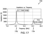
- FIG. 17 is a graph 1700 of impedance versus frequency of one particular embodiment of inductive-capacitive filter assembly 1400 with first insulating-conductive strip 1402 electrically coupled in series with second insulating-conductive strip 1403 as illustrated in FIG. 15 .
- this particular embodiment has a first resonant frequency 1702 of about 5.7 MHz and a second resonant frequency 1704 of about 15.6 MHz.
- First resonant frequency 1702 is a resonant frequency associated with second inductive-capacitive filter 1407
- second resonant frequency 1704 is a resonant frequency associated with first inductive-capacitive filter 1405.
- Peak impedance of first inductive-capacitive filter 1405 is about 6,200 ohms at second resonant frequency 1704, and peak impedance of second inductive-capacitive filter 1407 is about 22,000 ohms at first resonant frequency 1702.
- FIG. 18 illustrates inductive-capacitive filter assembly 1400 with first insulating-conductive strip 1402 electrically coupled in parallel with second insulating-conductive strip 1403 by an electrical conductors 1802 and 1804, and
- FIG. 19 is a graph 1900 of impedance versus frequency of one particular embodiment of inductive-capacitive filter assembly 1400 with first insulating-conductive strip 1402 electrically coupled in parallel with second insulating-conductive strip 1403 as illustrated in FIG. 18 .
- this particular embodiment has a resonant frequency 1902 of 8.6 MHz and a peak impedance of about 6,600 ohms at resonant frequency 1902.
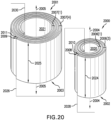
- FIG. 20 is a perspective view of a first inductive-capacitive filter 2000 and a second inductive-capacitive filter 2001 electrically coupled in series by an electrical conductor 2026. Additional electrical conductors 2028 and 2030 provide electrical interface to first and second inductive-capacitive filters 2000 and 2001, respectively.
- First inductive-capacitive filter 2000 includes a first insulating-conductive strip 2002
- second inductive-capacitive filter 2001 includes a second insulating-conductive strip 2003.
- First insulating-conductive strip 2002 includes an insulating strip 2008 wound in parallel with a conductive strip 2010 around a winding axis 2004, and second insulating-conductive strip 2003 includes an insulating strip 2009 wound in parallel with a conductive strip 2011 around a winding axis 2005.
- Each of the first insulating-conductive strip 2002 and second insulating-conductive strip 2003 has, for example, a configuration similar to one or more of the insulating-conductive strips discussed above with respect to FIGS. 1-19 .
- Bandstop characteristics can be varied during the design and/or manufacture of inductive-capacitive filters 2000 and/or 2001, for example, by (1) varying number of turns of first insulating-conductive strip 2002 and/or second insulating-conductive strip 2003, (2) varying the size and/or shape of a inner aperture 2020 and 2021 of inductive-capacitive filters 2000 and 2001, (3) varying thickness and/or dielectric properties of insulating strip 2008 and/or insulating strip 2009, (4) varying thickness of conductive strip 2010 and/or conductive strip 2011, and/or (5) and/or varying a width 2024 and/or width 2025 of first and second insulating-conductive strip 2002 and 2003, respectively, such as in a manner similar to that discussed above with respect to FIGS.
- first and second insulating-conductive strips 2002 and 2003 are illustrated as forming three and four turns 2006 and 2007, respectively, the number of turns of first and second insulating-conductive strips 2002 and 2003 may be varied without departing from the scope hereof. Only some instances of turns 2006 and 2007 are labeled in FIG. 20 to promote illustrative clarity.
- inductive-capacitive filter 2000 and/or 2001 could be modified to include one or more additional insulating-conductive strips departing from the scope hereof.
- first inductive-capacitive filter 2000 and a second inductive-capacitive filter 2001 could be electrically coupled in parallel without departing from the scope hereof.
- FIG. 21 is a graph 2100 of impedance versus frequency of one particular embodiment of the FIG. 20 inductive-capacitive filters 2000 and 2001 electrically coupled in series. As evident from FIG. 21 , this particular embodiment has a first resonant frequency 2102 of about 2 MHz and a second resonant frequency 2104 of about 26.6 MHz. First resonant frequency 2102 is a resonant frequency associated with second inductive-capacitive filter 2001, and second resonant frequency 2104 is a resonant frequency associated with first inductive-capacitive filter 2000.
- Peak impedance of first inductive-capacitive filter 2000 is about 39,250 ohms at second resonant frequency 2104, and peak impedance of second inductive-capacitive filter 2001 is about 16,095 ohms at first resonant frequency 2102.
- FIG. 22 is a perspective view of an inductive-capacitive filter assembly 2200 including three insulating-conductive strips 2202
- FIG. 23 is a cross-sectional view of inductive-capacitive filter assembly 2200 taken along line 23A-23A of FIG. 22 .
- Each insulating-conductive strip 2202 is similar to insulating-conductive strip 102.
- first insulating-conductive strip 2202(1) includes a first conductive strip 2210(1) joined with a first insulating strip 2208(1)
- second insulating-conductive strip 2202(2) includes a second conductive strip 2210(2) joined with a second insulating strip 2208(2)
- third insulating-conductive strip 2202(3) includes a third conductive strip 2210(3) joined with a third insulating strip 2208(3).
- each conductive strip 2210 includes opposing first and second terminals (not shown) electrically coupled to opposing ends of the conductive strip. Only some instances of insulating-conductive strips 2202, insulating strips 2208 and conductive strips 2210 are labeled in FIG. 23 to promote illustrative clarity. The number of insulating-conductive strips 2202 could be varied without departing from the scope hereof.
- Each conductive strip 2210 is used, for example, as a separate channel of a multi-channel bandstop filter, where each channel has similar bandstop characteristics.
- Bandstop characteristics can be varied during the design and/or manufacture of inductive-capacitive filter assembly 2200, for example, by (1) varying number of turns 2206 of insulating-conductive strips 2202, (2) varying the size and/or shape of a inner aperture 2220 of inductive-capacitive filter assembly 2200, (3) varying thickness and/or dielectric properties of insulating strips 2208, (4) varying thickness of conductive strips 2210, (5) and/or varying a width 2224 of insulating-conductive strips 2202, such as in a manner similar to that discussed above with respect to FIGS. 1-21 . Only two instances of turns 2206 are labeled in FIG. 22 to promote illustrative clarity.
- Inductive-capacitive filter assembly 2200 has an approximate electric model similar to that of FIG. 3 in applications where conductive strips 2210 are electrically coupled in parallel.
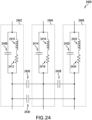
- FIG. 24 illustrates an approximate electrical model 2400 of inductive-capacitive filter assembly 2000 when conductive strips 2210 are not electrically coupled in parallel.
- inductive-capacitive filter assembly 2200 forms three channels 2402, 2404, and 2406 corresponding to insulating-conductive strips 2202(1), 2202(2), and 2202(3), respectively, such that each insulating-conductive strip 2202 forms a respective inductive-capacitive filter.
- Capacitor 2408, inductor 2410, and resistor 2412 represent capacitance, inductance, and resistance, respectively, of channel 2402.
- Capacitor 2414, inductor 2416, and resistor 2418 represent capacitance, inductance, and resistance, respectively, of channel 2404.
- Capacitor 2420, inductor 2422, and resistor 2424 represent capacitance, inductance, and resistance, respectively, of channel 2406.
- Capacitor 2426 represents capacitive coupling between channel 2402 and channel 2404
- capacitor 2428 represents capacitive coupling between channel 2404 and channel 2406
- capacitor 2430 represents capacitive coupling between channel 2402 and channel 2406.
- FIG. 25 is a cross-sectional view analogous to FIG. 2 of an inductive-capacitive filter 2500 which is like the FIG. 1 inductive-capacitive filter but including an insulating strip 2508 in place of insulating strip 108.
- Insulating strip 2508 has a width 2516 that is greater than a width 116 of conductive strip 110, such as to reduce the likelihood of accidental shorting of adjacent sections of conductive strip 110.
- Inductive-capacitive filters 100, 500, 600, 700, 800, 900, 1100, 1300, 1405, 1407, 2000, 2001, 2200, and 2500 do not have an explicit magnetic core, or in other words, these inductive-capacitive filters have an "air" core.
- any of the inductive-capacitive filters disclosed herein could be modified to include an explicit magnetic core formed of a magnetic material, including but not limited to a ferrite magnetic material or an iron powder magnetic material.
- the magnetic core which may form either a partial magnetic flux path or a complete magnetic flux path, affects the resonant frequency of the inductive-capacitive filter.
- inductance increases with decreased reluctance of the magnetic flux path of the inductive-capacitive filter, and increasing inductance decreases the filter's resonant frequency. Consequently, resonant frequency of an inductive-capacitive filter with a given magnetic core can be tuned by varying magnetic permeability of magnetic material forming the magnetic core, such that resonant frequency decreases with increasing magnetic permeability of the magnetic material.
- FIGS. 27-29 each illustrate a respective example of an inductive-capacitive filter with a magnetic core forming a complete magnetic path, or in other words, with a magnetic core forming a closed path around an insulating-conductive strip of the inductive-capacitive filter.
- FIG. 27 illustrates a perspective view of an inductive-capacitive filter 2700 which is like inductive-capacitive filter 100 of FIG. 1 but further including a magnetic core 2728.
- Magnetic core 2728 included an inner post (not visible in FIG. 27 ) extending through inner aperture 120 and an outer portion connecting opposing ends of the inner post.
- magnetic core 2728 is formed of two “E” cores, and in some other embodiments, magnetic core 2728 is formed of an "I" core and an "E” core.
- Magnetic core 2728 provides a lower-reluctance magnetic flux path than magnetic core 2628 of FIG. 26 , and therefore, inductive-capacitive filter 2700 of FIG. 27 will have a lower resonant frequency than inductive-capacitive filter 2600 of FIG. 26 .
- First and second terminals 134 and 136 are not shown in FIG. 27 to promote illustrative clarity.
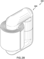
- FIG. 28 illustrates a perspective view of an inductive-capacitive filter 2800 which is like inductive-capacitive filter 100 of FIG. 1 but further including a magnetic core 2828.
- magnetic core 2828 is formed of two "U” cores, and in some other embodiments, magnetic core 2828 is formed of an "I" core and an "U” core.
- Magnetic core 2828 provides a lower-reluctance magnetic flux path than magnetic core 2628 of FIG. 26 , and therefore, inductive-capacitive filter 2800 of FIG. 28 will have a lower resonant frequency than inductive-capacitive filter 2600 of FIG. 26 .
- First and second terminals 134 and 136 are not shown in FIG. 28 to promote illustrative clarity.
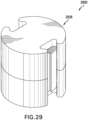
- FIG. 29 illustrates a perspective view of an inductive-capacitive filter 2900 which is like inductive-capacitive filter 100 of FIG. 1 but further including a magnetic core 2928.
- Magnetic core 2928 is similar to magnetic core 2728 of FIG. 27 but has a rounded outer portion connecting opposing ends of an inner post (not visible in FIG. 29 ) extending through inner aperture 120.
- magnetic core 2928 is formed of two pot cores. Magnetic core 2928 provides a lower-reluctance magnetic flux path than either magnetic core 2628 of FIG. 26 , magnetic core 2728 of FIG. 27 , or magnetic core 2828 of FIG. 28 , and therefore, inductive-capacitive filter 2900 of FIG.
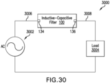
- FIG. 30 illustrates an electrical circuit 3000 including an instance of inductive-capacitive filter 100 electrically coupled in series with an alternating current (AC) electrical power source 3002 and a load 3004.
- Circuit 3000 is, for example, part of a semiconductor processing system.
- electrical power source 3002 represents an AC electric grid (e.g., operating at 50 or 60 Hertz), an AC generator, an inverter, an oscillator, an audio amplifier, or a radio-frequency amplifier
- load 3004 represents a linear load (e.g., resistive, inductive, and/or capacitive load) or a non-linear load (e.g., a switching power supply load).
- First end 130 of conductive strip 110 of inductive-capacitive filter 100 is electrically coupled to electrical power source 3002 via first terminal 134 at a first node 3006, and second end 132 of conductive strip 110 is electrically coupled to load 3004 via terminal 136 at a second node 3008, in electrical circuit 3000.
- first and second ends 130 and 132 of conductive strip 110 are electrically coupled to different respective nodes 3006 and 3008 of electrical circuit 3000.
- inductive-capacitive filter 100 blocks transmission of signals within a particular frequency band near filter 100's resonant frequency, such as to prevent transmission of undesired signals generated by electric power source 3002 or by load 3004.
- Inductive-capacitive filter 100 is tuned, for example, to have a resonant frequency near or equal to the frequency of the undesired signals, such that inductive-capacitive filter 100 has a high-impedance at this frequency and thereby substantially blocks transmission of the undesired signals in electrical circuit 3000.
- AC electrical power source 3002 could be replaced with a direct current (DC) electrical power source without departing from the scope hereof.
- FIG. 31 illustrates an electrical circuit 3100 which is like electrical circuit 3000 of FIG. 30 but with AC electrical power source 3002 replace with a direct current (DC) electric power source 3102.
- DC electric power source 3102 is, for example, a DC electric power buss, a power supply, a battery, or one or more photovoltaic cells.
- load 3004 is a power supply which generates an AC output signal at a frequency f 1 for powering external circuitry (not shown).
- This power supply is sensitive to noise from AC electric power source 3002 or DC electric power source 2802 having a frequency f 1 , and inductive-capacitive filter 100 is accordingly tuned to block transmission of signals having a frequency f 1 .
- Electrical circuits 3000 and 3100 could be modified to replace inductive-capacitive filter 100 with any of the other inductive-capacitive filters disclosed herein without departing from the scope hereof. Additionally, the topology of electrical circuits 3000 and 2100 could be modified without departing from the scope hereof. For example, electrical circuit 3000 could be modified such that inductive-capacitive filter 100 is electrically coupled in parallel with each of electrical power source 3002 and load 3104, to shunt all signals except those having a frequency near the resonant frequency of inductive-capacitive filter 100.
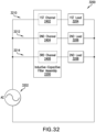
- FIG. 32 illustrates an electrical circuit 3200 including an instance of inductive-capacitive filter assembly 2200, an AC electrical power source 3202, a first load 3204, a second load 3206, and a third load 3208.
- First channel 2402 of inductive-capacitive filter assembly 2200 is electrically coupled between AC electrical power source 3202 and first load 3204 in a first branch 3210 of electrical circuit 3200
- second channel 2404 of inductive-capacitive filter assembly 2200 is electrically coupled between AC electrical power source 3202 and second load 3206 in a second branch 3212 of electrical circuit 3200
- third channel 2406 of inductive-capacitive filter assembly 2200 is electrically coupled between AC electrical power source 3202 and third load 3208 in a third branch 3208 of electrical circuit 3200.
- Circuit 3200 is, for example, part of a semiconductor processing system.
- AC electrical power source 3202 may be replaced with a DC electrical power source without departing from the scope hereof.
- first load 3204 is a first power supply which generates an AC output signal at a first frequency f 1 for powering external circuitry (not shown)
- second load 3206 is a second power supply which generates an AC output signal at a second frequency f 2 for powering external circuitry (not shown)
- third load 3208 is a third power supply which generates an AC output signal at a third frequency f 3 for powering external circuitry (not shown).
- the first, second, and third power supplies are sensitive to noise from AC electrical power source 3202 having a frequency f 1 , a frequency f 2 , and a frequency f 3 , respectively.
- first channel 2402 of inductive-capacitive filter 2200 is tuned to block transmission of signals having a frequency f 1
- second channel 2404 of inductive-capacitive filter 2200 is tuned to block transmission of signals having a frequency f 2
- third channel 2406 of inductive-capacitive filter 2200 is tuned to block transmission of signals having a frequency f 3 , in this application.
- load 3304 is sensitive to noise from AC electrical power source 3302 having a frequency f 1 and noise from AC electrical power source 3302 having a frequency f 2 . Accordingly, first inductive-capacitive filter 1405 is tuned to block transmission of signals having a frequency f 1 , and second inductive-capacitive filter 1407 is tuned to block transmission of signals having a frequency f 2 , in this application.
Landscapes
- Filters And Equalizers (AREA)
- Coils Or Transformers For Communication (AREA)
- Fixed Capacitors And Capacitor Manufacturing Machines (AREA)
- Control Of Motors That Do Not Use Commutators (AREA)
- Coils Of Transformers For General Uses (AREA)
- Insulating Of Coils (AREA)
Priority Applications (1)
| Application Number | Priority Date | Filing Date | Title |
|---|---|---|---|
| EP23163386.8A EP4220956A3 (en) | 2017-07-25 | 2018-07-25 | Inductive-capacitive filters and associated systems and methods |
Applications Claiming Priority (2)
| Application Number | Priority Date | Filing Date | Title |
|---|---|---|---|
| US201762536806P | 2017-07-25 | 2017-07-25 | |
| PCT/US2018/043651 WO2019023325A1 (en) | 2017-07-25 | 2018-07-25 | INDUCTIVE-CAPACITIVE FILTERS AND ASSOCIATED SYSTEMS AND METHODS |
Related Child Applications (2)
| Application Number | Title | Priority Date | Filing Date |
|---|---|---|---|
| EP23163386.8A Division-Into EP4220956A3 (en) | 2017-07-25 | 2018-07-25 | Inductive-capacitive filters and associated systems and methods |
| EP23163386.8A Division EP4220956A3 (en) | 2017-07-25 | 2018-07-25 | Inductive-capacitive filters and associated systems and methods |
Publications (3)
| Publication Number | Publication Date |
|---|---|
| EP3659255A1 EP3659255A1 (en) | 2020-06-03 |
| EP3659255A4 EP3659255A4 (en) | 2021-10-27 |
| EP3659255B1 true EP3659255B1 (en) | 2023-05-03 |
Family
ID=65040341
Family Applications (2)
| Application Number | Title | Priority Date | Filing Date |
|---|---|---|---|
| EP18837308.8A Active EP3659255B1 (en) | 2017-07-25 | 2018-07-25 | Inductive-capacitive filters and associated systems and methods |
| EP23163386.8A Pending EP4220956A3 (en) | 2017-07-25 | 2018-07-25 | Inductive-capacitive filters and associated systems and methods |
Family Applications After (1)
| Application Number | Title | Priority Date | Filing Date |
|---|---|---|---|
| EP23163386.8A Pending EP4220956A3 (en) | 2017-07-25 | 2018-07-25 | Inductive-capacitive filters and associated systems and methods |
Country Status (5)
| Country | Link |
|---|---|
| US (2) | US11183985B2 (https=) |
| EP (2) | EP3659255B1 (https=) |
| JP (3) | JP7231629B2 (https=) |
| CN (2) | CN116886065A (https=) |
| WO (1) | WO2019023325A1 (https=) |
Families Citing this family (2)
| Publication number | Priority date | Publication date | Assignee | Title |
|---|---|---|---|---|
| WO2019023325A1 (en) | 2017-07-25 | 2019-01-31 | Wjlp Company Inc. | INDUCTIVE-CAPACITIVE FILTERS AND ASSOCIATED SYSTEMS AND METHODS |
| US11831290B2 (en) * | 2017-07-25 | 2023-11-28 | Wjlp Company Inc. | Inductive-capacitive filters and associated systems and methods |
Family Cites Families (27)
| Publication number | Priority date | Publication date | Assignee | Title |
|---|---|---|---|---|
| US2027067A (en) * | 1930-11-05 | 1936-01-07 | Siemens Ag | Filter circuit |
| US2884605A (en) * | 1953-09-11 | 1959-04-28 | Cornell Dubilier Electric | Electrical suppressor |
| US3911332A (en) | 1971-12-29 | 1975-10-07 | George M Kunkel | Wound transformers and machine for making the same |
| US4048593A (en) * | 1974-05-13 | 1977-09-13 | Zillman Jack H | Electrical component for providing integrated inductive-capacitive networks |
| JPS5483736A (en) * | 1977-12-16 | 1979-07-04 | Matsushita Electric Ind Co Ltd | Noise filter |
| JP2770278B2 (ja) | 1987-01-14 | 1998-06-25 | 毅 池田 | ノイズ・フイルタ及びその製造方法 |
| DE3909528A1 (de) | 1988-03-23 | 1989-10-12 | Murata Manufacturing Co | Stoerschutzfilter |
| JP2728439B2 (ja) * | 1988-07-14 | 1998-03-18 | 毅 池田 | 4端子型ノイズフィルタおよびその製造方法 |
| JPH0817131B2 (ja) | 1989-01-12 | 1996-02-21 | 株式会社村田製作所 | フライバックトランス |
| US5153812A (en) * | 1989-06-16 | 1992-10-06 | Mitsubishi Denki Kabushiki Kaisha | Composite LC element |
| JPH04199502A (ja) | 1990-11-29 | 1992-07-20 | Mitsubishi Electric Corp | Lc複合素子 |
| JP3184580B2 (ja) * | 1991-10-29 | 2001-07-09 | 新潟精密株式会社 | 共振フィルタ |
| JPH05251267A (ja) * | 1992-03-06 | 1993-09-28 | Okaya Electric Ind Co Ltd | 複合電子部品 |
| US5337028A (en) * | 1992-05-27 | 1994-08-09 | Sundstrand Corporation | Multilayered distributed filter |
| JPH0745476A (ja) * | 1993-07-26 | 1995-02-14 | Alps Electric Co Ltd | Lcフィルタおよびその製造方法 |
| JPH07122460A (ja) * | 1993-10-21 | 1995-05-12 | Niigata Seimitsu Kk | Lcノイズフィルタおよびその製造方法 |
| JP3512472B2 (ja) * | 1994-06-06 | 2004-03-29 | 新潟精密株式会社 | 正弦波発振回路 |
| JPH08162367A (ja) * | 1994-12-08 | 1996-06-21 | Nissei Denki Kk | ノイズフイルタ |
| US6208225B1 (en) * | 1999-02-25 | 2001-03-27 | Formfactor, Inc. | Filter structures for integrated circuit interfaces |
| CN1161880C (zh) * | 1999-09-21 | 2004-08-11 | 株式会社村田制作所 | 电感电容滤波器 |
| CN2472352Y (zh) | 2001-03-22 | 2002-01-16 | 尤大千 | 分布式级联l-c一体化滤波器 |
| JP4245930B2 (ja) | 2003-01-30 | 2009-04-02 | 日置電機株式会社 | 分布定数型フィルタ素子 |
| JP2007067800A (ja) | 2005-08-31 | 2007-03-15 | Tdk Corp | Lc複合素子 |
| NZ575304A (en) | 2009-03-03 | 2011-02-25 | Eaton Ind Co | Series resonant power convertor with composite spiral wound inductor/capacitor |
| EP3269419A1 (en) * | 2013-08-04 | 2018-01-17 | Greatbatch Ltd. | Multilayer planar spiral inductor filter for medical, therapeutic or diagnostic applications |
| US11831290B2 (en) * | 2017-07-25 | 2023-11-28 | Wjlp Company Inc. | Inductive-capacitive filters and associated systems and methods |
| WO2019023325A1 (en) | 2017-07-25 | 2019-01-31 | Wjlp Company Inc. | INDUCTIVE-CAPACITIVE FILTERS AND ASSOCIATED SYSTEMS AND METHODS |
-
2018
- 2018-07-25 WO PCT/US2018/043651 patent/WO2019023325A1/en not_active Ceased
- 2018-07-25 CN CN202311050720.4A patent/CN116886065A/zh active Pending
- 2018-07-25 EP EP18837308.8A patent/EP3659255B1/en active Active
- 2018-07-25 US US16/633,409 patent/US11183985B2/en active Active
- 2018-07-25 CN CN201880048147.4A patent/CN110945784B/zh active Active
- 2018-07-25 JP JP2020527840A patent/JP7231629B2/ja active Active
- 2018-07-25 EP EP23163386.8A patent/EP4220956A3/en active Pending
-
2023
- 2023-02-16 JP JP2023022186A patent/JP7591073B2/ja active Active
- 2023-11-27 US US18/519,421 patent/US12537497B2/en active Active
-
2024
- 2024-11-15 JP JP2024199678A patent/JP2025024714A/ja active Pending
Also Published As
| Publication number | Publication date |
|---|---|
| US20240106405A1 (en) | 2024-03-28 |
| JP7231629B2 (ja) | 2023-03-01 |
| JP7591073B2 (ja) | 2024-11-27 |
| EP3659255A1 (en) | 2020-06-03 |
| US11183985B2 (en) | 2021-11-23 |
| EP4220956A3 (en) | 2023-08-09 |
| JP2020529177A (ja) | 2020-10-01 |
| US12537497B2 (en) | 2026-01-27 |
| CN116886065A (zh) | 2023-10-13 |
| EP4220956A2 (en) | 2023-08-02 |
| US20200366262A1 (en) | 2020-11-19 |
| WO2019023325A1 (en) | 2019-01-31 |
| CN110945784B (zh) | 2023-08-22 |
| EP3659255A4 (en) | 2021-10-27 |
| CN110945784A (zh) | 2020-03-31 |
| JP2023059922A (ja) | 2023-04-27 |
| JP2025024714A (ja) | 2025-02-20 |
Similar Documents
| Publication | Publication Date | Title |
|---|---|---|
| JP6937741B2 (ja) | 磁界結合を用いたワイヤレス電力伝送に供されるシングルレイヤマルチモードアンテナ | |
| US8988167B2 (en) | RF signal blocking device | |
| KR102075284B1 (ko) | 시간 지연 필터 | |
| US12537497B2 (en) | Inductive-capacitive filters and associated systems and methods | |
| US9385682B2 (en) | High frequency component and filter component | |
| US20030001709A1 (en) | Multiple-interleaved integrated circuit transformer | |
| US20190393604A1 (en) | Antenna device, communication system, and electronic apparatus | |
| JP5252564B2 (ja) | インダクタンス素子 | |
| WO2005048451A1 (en) | Communication transformer | |
| US11908603B2 (en) | Inductor and voltage converter using it | |
| US11831290B2 (en) | Inductive-capacitive filters and associated systems and methods | |
| JP2020529177A5 (https=) | ||
| JP6221240B2 (ja) | コイル部品 | |
| AU2012215196B2 (en) | Filter for a magnetron power supply lead | |
| US8421575B1 (en) | Multi-layered circuit structure | |
| JP2005123751A (ja) | 電気的雑音フィルタ及び電気的雑音除去方法 | |
| Koochakzadeh et al. | Design of band-select filters with arbitrary characteristics using overlapped loaded line topologies | |
| WO1997045889A2 (en) | Improved transmission line |
Legal Events
| Date | Code | Title | Description |
|---|---|---|---|
| STAA | Information on the status of an ep patent application or granted ep patent |
Free format text: STATUS: THE INTERNATIONAL PUBLICATION HAS BEEN MADE |
|
| PUAI | Public reference made under article 153(3) epc to a published international application that has entered the european phase |
Free format text: ORIGINAL CODE: 0009012 |
|
| STAA | Information on the status of an ep patent application or granted ep patent |
Free format text: STATUS: REQUEST FOR EXAMINATION WAS MADE |
|
| 17P | Request for examination filed |
Effective date: 20200129 |
|
| AK | Designated contracting states |
Kind code of ref document: A1 Designated state(s): AL AT BE BG CH CY CZ DE DK EE ES FI FR GB GR HR HU IE IS IT LI LT LU LV MC MK MT NL NO PL PT RO RS SE SI SK SM TR |
|
| AX | Request for extension of the european patent |
Extension state: BA ME |
|
| DAV | Request for validation of the european patent (deleted) | ||
| DAX | Request for extension of the european patent (deleted) | ||
| A4 | Supplementary search report drawn up and despatched |
Effective date: 20210923 |
|
| RIC1 | Information provided on ipc code assigned before grant |
Ipc: H03H 1/00 20060101ALI20210917BHEP Ipc: H03H 7/01 20060101ALI20210917BHEP Ipc: H03H 7/12 20060101ALI20210917BHEP Ipc: H03H 7/09 20060101AFI20210917BHEP |
|
| STAA | Information on the status of an ep patent application or granted ep patent |
Free format text: STATUS: EXAMINATION IS IN PROGRESS |
|
| 17Q | First examination report despatched |
Effective date: 20220401 |
|
| GRAP | Despatch of communication of intention to grant a patent |
Free format text: ORIGINAL CODE: EPIDOSNIGR1 |
|
| STAA | Information on the status of an ep patent application or granted ep patent |
Free format text: STATUS: GRANT OF PATENT IS INTENDED |
|
| INTG | Intention to grant announced |
Effective date: 20221130 |
|
| GRAS | Grant fee paid |
Free format text: ORIGINAL CODE: EPIDOSNIGR3 |
|
| GRAA | (expected) grant |
Free format text: ORIGINAL CODE: 0009210 |
|
| STAA | Information on the status of an ep patent application or granted ep patent |
Free format text: STATUS: THE PATENT HAS BEEN GRANTED |
|
| AK | Designated contracting states |
Kind code of ref document: B1 Designated state(s): AL AT BE BG CH CY CZ DE DK EE ES FI FR GB GR HR HU IE IS IT LI LT LU LV MC MK MT NL NO PL PT RO RS SE SI SK SM TR |
|
| REG | Reference to a national code |
Ref country code: GB Ref legal event code: FG4D |
|
| REG | Reference to a national code |
Ref country code: DE Ref legal event code: R096 Ref document number: 602018049355 Country of ref document: DE |
|
| REG | Reference to a national code |
Ref country code: AT Ref legal event code: REF Ref document number: 1565540 Country of ref document: AT Kind code of ref document: T Effective date: 20230515 Ref country code: CH Ref legal event code: EP |
|
| REG | Reference to a national code |
Ref country code: IE Ref legal event code: FG4D |
|
| P01 | Opt-out of the competence of the unified patent court (upc) registered |
Effective date: 20230523 |
|
| REG | Reference to a national code |
Ref country code: NL Ref legal event code: FP |
|
| REG | Reference to a national code |
Ref country code: LT Ref legal event code: MG9D |
|
| REG | Reference to a national code |
Ref country code: AT Ref legal event code: MK05 Ref document number: 1565540 Country of ref document: AT Kind code of ref document: T Effective date: 20230503 |
|
| PG25 | Lapsed in a contracting state [announced via postgrant information from national office to epo] |
Ref country code: SE Free format text: LAPSE BECAUSE OF FAILURE TO SUBMIT A TRANSLATION OF THE DESCRIPTION OR TO PAY THE FEE WITHIN THE PRESCRIBED TIME-LIMIT Effective date: 20230503 Ref country code: PT Free format text: LAPSE BECAUSE OF FAILURE TO SUBMIT A TRANSLATION OF THE DESCRIPTION OR TO PAY THE FEE WITHIN THE PRESCRIBED TIME-LIMIT Effective date: 20230904 Ref country code: NO Free format text: LAPSE BECAUSE OF FAILURE TO SUBMIT A TRANSLATION OF THE DESCRIPTION OR TO PAY THE FEE WITHIN THE PRESCRIBED TIME-LIMIT Effective date: 20230803 Ref country code: ES Free format text: LAPSE BECAUSE OF FAILURE TO SUBMIT A TRANSLATION OF THE DESCRIPTION OR TO PAY THE FEE WITHIN THE PRESCRIBED TIME-LIMIT Effective date: 20230503 Ref country code: AT Free format text: LAPSE BECAUSE OF FAILURE TO SUBMIT A TRANSLATION OF THE DESCRIPTION OR TO PAY THE FEE WITHIN THE PRESCRIBED TIME-LIMIT Effective date: 20230503 |
|
| PG25 | Lapsed in a contracting state [announced via postgrant information from national office to epo] |
Ref country code: RS Free format text: LAPSE BECAUSE OF FAILURE TO SUBMIT A TRANSLATION OF THE DESCRIPTION OR TO PAY THE FEE WITHIN THE PRESCRIBED TIME-LIMIT Effective date: 20230503 Ref country code: PL Free format text: LAPSE BECAUSE OF FAILURE TO SUBMIT A TRANSLATION OF THE DESCRIPTION OR TO PAY THE FEE WITHIN THE PRESCRIBED TIME-LIMIT Effective date: 20230503 Ref country code: LV Free format text: LAPSE BECAUSE OF FAILURE TO SUBMIT A TRANSLATION OF THE DESCRIPTION OR TO PAY THE FEE WITHIN THE PRESCRIBED TIME-LIMIT Effective date: 20230503 Ref country code: LT Free format text: LAPSE BECAUSE OF FAILURE TO SUBMIT A TRANSLATION OF THE DESCRIPTION OR TO PAY THE FEE WITHIN THE PRESCRIBED TIME-LIMIT Effective date: 20230503 Ref country code: IS Free format text: LAPSE BECAUSE OF FAILURE TO SUBMIT A TRANSLATION OF THE DESCRIPTION OR TO PAY THE FEE WITHIN THE PRESCRIBED TIME-LIMIT Effective date: 20230903 Ref country code: HR Free format text: LAPSE BECAUSE OF FAILURE TO SUBMIT A TRANSLATION OF THE DESCRIPTION OR TO PAY THE FEE WITHIN THE PRESCRIBED TIME-LIMIT Effective date: 20230503 Ref country code: GR Free format text: LAPSE BECAUSE OF FAILURE TO SUBMIT A TRANSLATION OF THE DESCRIPTION OR TO PAY THE FEE WITHIN THE PRESCRIBED TIME-LIMIT Effective date: 20230804 |
|
| PG25 | Lapsed in a contracting state [announced via postgrant information from national office to epo] |
Ref country code: FI Free format text: LAPSE BECAUSE OF FAILURE TO SUBMIT A TRANSLATION OF THE DESCRIPTION OR TO PAY THE FEE WITHIN THE PRESCRIBED TIME-LIMIT Effective date: 20230503 |
|
| PG25 | Lapsed in a contracting state [announced via postgrant information from national office to epo] |
Ref country code: SK Free format text: LAPSE BECAUSE OF FAILURE TO SUBMIT A TRANSLATION OF THE DESCRIPTION OR TO PAY THE FEE WITHIN THE PRESCRIBED TIME-LIMIT Effective date: 20230503 |
|
| PG25 | Lapsed in a contracting state [announced via postgrant information from national office to epo] |
Ref country code: SM Free format text: LAPSE BECAUSE OF FAILURE TO SUBMIT A TRANSLATION OF THE DESCRIPTION OR TO PAY THE FEE WITHIN THE PRESCRIBED TIME-LIMIT Effective date: 20230503 Ref country code: SK Free format text: LAPSE BECAUSE OF FAILURE TO SUBMIT A TRANSLATION OF THE DESCRIPTION OR TO PAY THE FEE WITHIN THE PRESCRIBED TIME-LIMIT Effective date: 20230503 Ref country code: RO Free format text: LAPSE BECAUSE OF FAILURE TO SUBMIT A TRANSLATION OF THE DESCRIPTION OR TO PAY THE FEE WITHIN THE PRESCRIBED TIME-LIMIT Effective date: 20230503 Ref country code: EE Free format text: LAPSE BECAUSE OF FAILURE TO SUBMIT A TRANSLATION OF THE DESCRIPTION OR TO PAY THE FEE WITHIN THE PRESCRIBED TIME-LIMIT Effective date: 20230503 Ref country code: DK Free format text: LAPSE BECAUSE OF FAILURE TO SUBMIT A TRANSLATION OF THE DESCRIPTION OR TO PAY THE FEE WITHIN THE PRESCRIBED TIME-LIMIT Effective date: 20230503 Ref country code: CZ Free format text: LAPSE BECAUSE OF FAILURE TO SUBMIT A TRANSLATION OF THE DESCRIPTION OR TO PAY THE FEE WITHIN THE PRESCRIBED TIME-LIMIT Effective date: 20230503 |
|
| REG | Reference to a national code |
Ref country code: DE Ref legal event code: R097 Ref document number: 602018049355 Country of ref document: DE |
|
| PG25 | Lapsed in a contracting state [announced via postgrant information from national office to epo] |
Ref country code: MC Free format text: LAPSE BECAUSE OF FAILURE TO SUBMIT A TRANSLATION OF THE DESCRIPTION OR TO PAY THE FEE WITHIN THE PRESCRIBED TIME-LIMIT Effective date: 20230503 |
|
| PG25 | Lapsed in a contracting state [announced via postgrant information from national office to epo] |
Ref country code: MC Free format text: LAPSE BECAUSE OF FAILURE TO SUBMIT A TRANSLATION OF THE DESCRIPTION OR TO PAY THE FEE WITHIN THE PRESCRIBED TIME-LIMIT Effective date: 20230503 |
|
| PLBE | No opposition filed within time limit |
Free format text: ORIGINAL CODE: 0009261 |
|
| STAA | Information on the status of an ep patent application or granted ep patent |
Free format text: STATUS: NO OPPOSITION FILED WITHIN TIME LIMIT |
|
| PG25 | Lapsed in a contracting state [announced via postgrant information from national office to epo] |
Ref country code: LU Free format text: LAPSE BECAUSE OF NON-PAYMENT OF DUE FEES Effective date: 20230725 |
|
| PG25 | Lapsed in a contracting state [announced via postgrant information from national office to epo] |
Ref country code: LU Free format text: LAPSE BECAUSE OF NON-PAYMENT OF DUE FEES Effective date: 20230725 |
|
| 26N | No opposition filed |
Effective date: 20240206 |
|
| GBPC | Gb: european patent ceased through non-payment of renewal fee |
Effective date: 20230803 |
|
| PG25 | Lapsed in a contracting state [announced via postgrant information from national office to epo] |
Ref country code: SI Free format text: LAPSE BECAUSE OF FAILURE TO SUBMIT A TRANSLATION OF THE DESCRIPTION OR TO PAY THE FEE WITHIN THE PRESCRIBED TIME-LIMIT Effective date: 20230503 |
|
| PG25 | Lapsed in a contracting state [announced via postgrant information from national office to epo] |
Ref country code: SI Free format text: LAPSE BECAUSE OF FAILURE TO SUBMIT A TRANSLATION OF THE DESCRIPTION OR TO PAY THE FEE WITHIN THE PRESCRIBED TIME-LIMIT Effective date: 20230503 Ref country code: IT Free format text: LAPSE BECAUSE OF FAILURE TO SUBMIT A TRANSLATION OF THE DESCRIPTION OR TO PAY THE FEE WITHIN THE PRESCRIBED TIME-LIMIT Effective date: 20230503 |
|
| PG25 | Lapsed in a contracting state [announced via postgrant information from national office to epo] |
Ref country code: GB Free format text: LAPSE BECAUSE OF NON-PAYMENT OF DUE FEES Effective date: 20230803 |
|
| PG25 | Lapsed in a contracting state [announced via postgrant information from national office to epo] |
Ref country code: GB Free format text: LAPSE BECAUSE OF NON-PAYMENT OF DUE FEES Effective date: 20230803 |
|
| PG25 | Lapsed in a contracting state [announced via postgrant information from national office to epo] |
Ref country code: BG Free format text: LAPSE BECAUSE OF FAILURE TO SUBMIT A TRANSLATION OF THE DESCRIPTION OR TO PAY THE FEE WITHIN THE PRESCRIBED TIME-LIMIT Effective date: 20230503 |
|
| PG25 | Lapsed in a contracting state [announced via postgrant information from national office to epo] |
Ref country code: BG Free format text: LAPSE BECAUSE OF FAILURE TO SUBMIT A TRANSLATION OF THE DESCRIPTION OR TO PAY THE FEE WITHIN THE PRESCRIBED TIME-LIMIT Effective date: 20230503 |
|
| PGFP | Annual fee paid to national office [announced via postgrant information from national office to epo] |
Ref country code: NL Payment date: 20250613 Year of fee payment: 8 Ref country code: BE Payment date: 20250619 Year of fee payment: 8 |
|
| PGFP | Annual fee paid to national office [announced via postgrant information from national office to epo] |
Ref country code: FR Payment date: 20250610 Year of fee payment: 8 |
|
| PG25 | Lapsed in a contracting state [announced via postgrant information from national office to epo] |
Ref country code: CY Free format text: LAPSE BECAUSE OF FAILURE TO SUBMIT A TRANSLATION OF THE DESCRIPTION OR TO PAY THE FEE WITHIN THE PRESCRIBED TIME-LIMIT; INVALID AB INITIO Effective date: 20180725 |
|
| PGFP | Annual fee paid to national office [announced via postgrant information from national office to epo] |
Ref country code: IE Payment date: 20250610 Year of fee payment: 8 |
|
| PG25 | Lapsed in a contracting state [announced via postgrant information from national office to epo] |
Ref country code: HU Free format text: LAPSE BECAUSE OF FAILURE TO SUBMIT A TRANSLATION OF THE DESCRIPTION OR TO PAY THE FEE WITHIN THE PRESCRIBED TIME-LIMIT; INVALID AB INITIO Effective date: 20180725 |
|
| PGFP | Annual fee paid to national office [announced via postgrant information from national office to epo] |
Ref country code: DE Payment date: 20250604 Year of fee payment: 8 |
|
| PGFP | Annual fee paid to national office [announced via postgrant information from national office to epo] |
Ref country code: CH Payment date: 20250801 Year of fee payment: 8 |
|
| PG25 | Lapsed in a contracting state [announced via postgrant information from national office to epo] |
Ref country code: TR Free format text: LAPSE BECAUSE OF FAILURE TO SUBMIT A TRANSLATION OF THE DESCRIPTION OR TO PAY THE FEE WITHIN THE PRESCRIBED TIME-LIMIT Effective date: 20230503 |