EP3640990A1 - Micro light emitting diode display panel and manufacturing method therefor - Google Patents
Micro light emitting diode display panel and manufacturing method therefor Download PDFInfo
- Publication number
- EP3640990A1 EP3640990A1 EP17911140.6A EP17911140A EP3640990A1 EP 3640990 A1 EP3640990 A1 EP 3640990A1 EP 17911140 A EP17911140 A EP 17911140A EP 3640990 A1 EP3640990 A1 EP 3640990A1
- Authority
- EP
- European Patent Office
- Prior art keywords
- layer
- emitting
- micro light
- electrode
- insulating layer
- Prior art date
- Legal status (The legal status is an assumption and is not a legal conclusion. Google has not performed a legal analysis and makes no representation as to the accuracy of the status listed.)
- Withdrawn
Links
Images




Classifications
-
- H—ELECTRICITY
- H10—SEMICONDUCTOR DEVICES; ELECTRIC SOLID-STATE DEVICES NOT OTHERWISE PROVIDED FOR
- H10H—INORGANIC LIGHT-EMITTING SEMICONDUCTOR DEVICES HAVING POTENTIAL BARRIERS
- H10H20/00—Individual inorganic light-emitting semiconductor devices having potential barriers, e.g. light-emitting diodes [LED]
- H10H20/80—Constructional details
- H10H20/85—Packages
- H10H20/857—Interconnections, e.g. lead-frames, bond wires or solder balls
-
- H—ELECTRICITY
- H10—SEMICONDUCTOR DEVICES; ELECTRIC SOLID-STATE DEVICES NOT OTHERWISE PROVIDED FOR
- H10H—INORGANIC LIGHT-EMITTING SEMICONDUCTOR DEVICES HAVING POTENTIAL BARRIERS
- H10H29/00—Integrated devices, or assemblies of multiple devices, comprising at least one light-emitting semiconductor element covered by group H10H20/00
- H10H29/20—Assemblies of multiple devices comprising at least one light-emitting semiconductor device covered by group H10H20/00
- H10H29/24—Assemblies of multiple devices comprising at least one light-emitting semiconductor device covered by group H10H20/00 comprising multiple light-emitting semiconductor devices
-
- H—ELECTRICITY
- H10—SEMICONDUCTOR DEVICES; ELECTRIC SOLID-STATE DEVICES NOT OTHERWISE PROVIDED FOR
- H10H—INORGANIC LIGHT-EMITTING SEMICONDUCTOR DEVICES HAVING POTENTIAL BARRIERS
- H10H29/00—Integrated devices, or assemblies of multiple devices, comprising at least one light-emitting semiconductor element covered by group H10H20/00
- H10H29/10—Integrated devices comprising at least one light-emitting semiconductor component covered by group H10H20/00
- H10H29/14—Integrated devices comprising at least one light-emitting semiconductor component covered by group H10H20/00 comprising multiple light-emitting semiconductor components
- H10H29/142—Two-dimensional arrangements, e.g. asymmetric LED layout
-
- H—ELECTRICITY
- H10—SEMICONDUCTOR DEVICES; ELECTRIC SOLID-STATE DEVICES NOT OTHERWISE PROVIDED FOR
- H10D—INORGANIC ELECTRIC SEMICONDUCTOR DEVICES
- H10D86/00—Integrated devices formed in or on insulating or conducting substrates, e.g. formed in silicon-on-insulator [SOI] substrates or on stainless steel or glass substrates
- H10D86/40—Integrated devices formed in or on insulating or conducting substrates, e.g. formed in silicon-on-insulator [SOI] substrates or on stainless steel or glass substrates characterised by multiple TFTs
-
- H—ELECTRICITY
- H10—SEMICONDUCTOR DEVICES; ELECTRIC SOLID-STATE DEVICES NOT OTHERWISE PROVIDED FOR
- H10D—INORGANIC ELECTRIC SEMICONDUCTOR DEVICES
- H10D86/00—Integrated devices formed in or on insulating or conducting substrates, e.g. formed in silicon-on-insulator [SOI] substrates or on stainless steel or glass substrates
- H10D86/40—Integrated devices formed in or on insulating or conducting substrates, e.g. formed in silicon-on-insulator [SOI] substrates or on stainless steel or glass substrates characterised by multiple TFTs
- H10D86/60—Integrated devices formed in or on insulating or conducting substrates, e.g. formed in silicon-on-insulator [SOI] substrates or on stainless steel or glass substrates characterised by multiple TFTs wherein the TFTs are in active matrices
-
- H—ELECTRICITY
- H10—SEMICONDUCTOR DEVICES; ELECTRIC SOLID-STATE DEVICES NOT OTHERWISE PROVIDED FOR
- H10H—INORGANIC LIGHT-EMITTING SEMICONDUCTOR DEVICES HAVING POTENTIAL BARRIERS
- H10H20/00—Individual inorganic light-emitting semiconductor devices having potential barriers, e.g. light-emitting diodes [LED]
- H10H20/01—Manufacture or treatment
- H10H20/011—Manufacture or treatment of bodies, e.g. forming semiconductor layers
- H10H20/018—Bonding of wafers
-
- H—ELECTRICITY
- H10—SEMICONDUCTOR DEVICES; ELECTRIC SOLID-STATE DEVICES NOT OTHERWISE PROVIDED FOR
- H10H—INORGANIC LIGHT-EMITTING SEMICONDUCTOR DEVICES HAVING POTENTIAL BARRIERS
- H10H20/00—Individual inorganic light-emitting semiconductor devices having potential barriers, e.g. light-emitting diodes [LED]
- H10H20/80—Constructional details
- H10H20/81—Bodies
- H10H20/819—Bodies characterised by their shape, e.g. curved or truncated substrates
-
- H—ELECTRICITY
- H10—SEMICONDUCTOR DEVICES; ELECTRIC SOLID-STATE DEVICES NOT OTHERWISE PROVIDED FOR
- H10H—INORGANIC LIGHT-EMITTING SEMICONDUCTOR DEVICES HAVING POTENTIAL BARRIERS
- H10H20/00—Individual inorganic light-emitting semiconductor devices having potential barriers, e.g. light-emitting diodes [LED]
- H10H20/80—Constructional details
- H10H20/83—Electrodes
-
- H—ELECTRICITY
- H10—SEMICONDUCTOR DEVICES; ELECTRIC SOLID-STATE DEVICES NOT OTHERWISE PROVIDED FOR
- H10H—INORGANIC LIGHT-EMITTING SEMICONDUCTOR DEVICES HAVING POTENTIAL BARRIERS
- H10H20/00—Individual inorganic light-emitting semiconductor devices having potential barriers, e.g. light-emitting diodes [LED]
- H10H20/80—Constructional details
- H10H20/83—Electrodes
- H10H20/831—Electrodes characterised by their shape
-
- H—ELECTRICITY
- H10—SEMICONDUCTOR DEVICES; ELECTRIC SOLID-STATE DEVICES NOT OTHERWISE PROVIDED FOR
- H10H—INORGANIC LIGHT-EMITTING SEMICONDUCTOR DEVICES HAVING POTENTIAL BARRIERS
- H10H20/00—Individual inorganic light-emitting semiconductor devices having potential barriers, e.g. light-emitting diodes [LED]
- H10H20/80—Constructional details
- H10H20/83—Electrodes
- H10H20/831—Electrodes characterised by their shape
- H10H20/8312—Electrodes characterised by their shape extending at least partially through the bodies
-
- H—ELECTRICITY
- H10—SEMICONDUCTOR DEVICES; ELECTRIC SOLID-STATE DEVICES NOT OTHERWISE PROVIDED FOR
- H10H—INORGANIC LIGHT-EMITTING SEMICONDUCTOR DEVICES HAVING POTENTIAL BARRIERS
- H10H20/00—Individual inorganic light-emitting semiconductor devices having potential barriers, e.g. light-emitting diodes [LED]
- H10H20/80—Constructional details
- H10H20/83—Electrodes
- H10H20/831—Electrodes characterised by their shape
- H10H20/8314—Electrodes characterised by their shape extending at least partially onto an outer side surface of the bodies
-
- H—ELECTRICITY
- H10—SEMICONDUCTOR DEVICES; ELECTRIC SOLID-STATE DEVICES NOT OTHERWISE PROVIDED FOR
- H10H—INORGANIC LIGHT-EMITTING SEMICONDUCTOR DEVICES HAVING POTENTIAL BARRIERS
- H10H20/00—Individual inorganic light-emitting semiconductor devices having potential barriers, e.g. light-emitting diodes [LED]
- H10H20/80—Constructional details
- H10H20/84—Coatings, e.g. passivation layers or antireflective coatings
-
- H—ELECTRICITY
- H10—SEMICONDUCTOR DEVICES; ELECTRIC SOLID-STATE DEVICES NOT OTHERWISE PROVIDED FOR
- H10H—INORGANIC LIGHT-EMITTING SEMICONDUCTOR DEVICES HAVING POTENTIAL BARRIERS
- H10H20/00—Individual inorganic light-emitting semiconductor devices having potential barriers, e.g. light-emitting diodes [LED]
- H10H20/80—Constructional details
- H10H20/85—Packages
- H10H20/8506—Containers
-
- H—ELECTRICITY
- H10—SEMICONDUCTOR DEVICES; ELECTRIC SOLID-STATE DEVICES NOT OTHERWISE PROVIDED FOR
- H10H—INORGANIC LIGHT-EMITTING SEMICONDUCTOR DEVICES HAVING POTENTIAL BARRIERS
- H10H29/00—Integrated devices, or assemblies of multiple devices, comprising at least one light-emitting semiconductor element covered by group H10H20/00
- H10H29/01—Manufacture or treatment
- H10H29/036—Manufacture or treatment of packages
- H10H29/0364—Manufacture or treatment of packages of interconnections
-
- H—ELECTRICITY
- H10—SEMICONDUCTOR DEVICES; ELECTRIC SOLID-STATE DEVICES NOT OTHERWISE PROVIDED FOR
- H10H—INORGANIC LIGHT-EMITTING SEMICONDUCTOR DEVICES HAVING POTENTIAL BARRIERS
- H10H29/00—Integrated devices, or assemblies of multiple devices, comprising at least one light-emitting semiconductor element covered by group H10H20/00
- H10H29/80—Constructional details
- H10H29/85—Packages
- H10H29/857—Interconnections
-
- H—ELECTRICITY
- H10—SEMICONDUCTOR DEVICES; ELECTRIC SOLID-STATE DEVICES NOT OTHERWISE PROVIDED FOR
- H10P—GENERIC PROCESSES OR APPARATUS FOR THE MANUFACTURE OR TREATMENT OF DEVICES COVERED BY CLASS H10
- H10P72/00—Handling or holding of wafers, substrates or devices during manufacture or treatment thereof
- H10P72/70—Handling or holding of wafers, substrates or devices during manufacture or treatment thereof for supporting or gripping
- H10P72/74—Handling or holding of wafers, substrates or devices during manufacture or treatment thereof for supporting or gripping using temporarily an auxiliary support
-
- H—ELECTRICITY
- H10—SEMICONDUCTOR DEVICES; ELECTRIC SOLID-STATE DEVICES NOT OTHERWISE PROVIDED FOR
- H10P—GENERIC PROCESSES OR APPARATUS FOR THE MANUFACTURE OR TREATMENT OF DEVICES COVERED BY CLASS H10
- H10P74/00—Testing or measuring during manufacture or treatment of wafers, substrates or devices
- H10P74/23—Testing or measuring during manufacture or treatment of wafers, substrates or devices characterised by multiple measurements, corrections, marking or sorting processes
-
- H—ELECTRICITY
- H10—SEMICONDUCTOR DEVICES; ELECTRIC SOLID-STATE DEVICES NOT OTHERWISE PROVIDED FOR
- H10P—GENERIC PROCESSES OR APPARATUS FOR THE MANUFACTURE OR TREATMENT OF DEVICES COVERED BY CLASS H10
- H10P74/00—Testing or measuring during manufacture or treatment of wafers, substrates or devices
- H10P74/27—Structural arrangements therefor
-
- H—ELECTRICITY
- H10—SEMICONDUCTOR DEVICES; ELECTRIC SOLID-STATE DEVICES NOT OTHERWISE PROVIDED FOR
- H10W—GENERIC PACKAGES, INTERCONNECTIONS, CONNECTORS OR OTHER CONSTRUCTIONAL DETAILS OF DEVICES COVERED BY CLASS H10
- H10W90/00—Package configurations
-
- H—ELECTRICITY
- H10—SEMICONDUCTOR DEVICES; ELECTRIC SOLID-STATE DEVICES NOT OTHERWISE PROVIDED FOR
- H10H—INORGANIC LIGHT-EMITTING SEMICONDUCTOR DEVICES HAVING POTENTIAL BARRIERS
- H10H20/00—Individual inorganic light-emitting semiconductor devices having potential barriers, e.g. light-emitting diodes [LED]
- H10H20/01—Manufacture or treatment
-
- H—ELECTRICITY
- H10—SEMICONDUCTOR DEVICES; ELECTRIC SOLID-STATE DEVICES NOT OTHERWISE PROVIDED FOR
- H10H—INORGANIC LIGHT-EMITTING SEMICONDUCTOR DEVICES HAVING POTENTIAL BARRIERS
- H10H20/00—Individual inorganic light-emitting semiconductor devices having potential barriers, e.g. light-emitting diodes [LED]
- H10H20/01—Manufacture or treatment
- H10H20/032—Manufacture or treatment of electrodes
-
- H—ELECTRICITY
- H10—SEMICONDUCTOR DEVICES; ELECTRIC SOLID-STATE DEVICES NOT OTHERWISE PROVIDED FOR
- H10H—INORGANIC LIGHT-EMITTING SEMICONDUCTOR DEVICES HAVING POTENTIAL BARRIERS
- H10H20/00—Individual inorganic light-emitting semiconductor devices having potential barriers, e.g. light-emitting diodes [LED]
- H10H20/01—Manufacture or treatment
- H10H20/034—Manufacture or treatment of coatings
-
- H—ELECTRICITY
- H10—SEMICONDUCTOR DEVICES; ELECTRIC SOLID-STATE DEVICES NOT OTHERWISE PROVIDED FOR
- H10H—INORGANIC LIGHT-EMITTING SEMICONDUCTOR DEVICES HAVING POTENTIAL BARRIERS
- H10H20/00—Individual inorganic light-emitting semiconductor devices having potential barriers, e.g. light-emitting diodes [LED]
- H10H20/01—Manufacture or treatment
- H10H20/036—Manufacture or treatment of packages
- H10H20/0364—Manufacture or treatment of packages of interconnections
-
- H—ELECTRICITY
- H10—SEMICONDUCTOR DEVICES; ELECTRIC SOLID-STATE DEVICES NOT OTHERWISE PROVIDED FOR
- H10P—GENERIC PROCESSES OR APPARATUS FOR THE MANUFACTURE OR TREATMENT OF DEVICES COVERED BY CLASS H10
- H10P72/00—Handling or holding of wafers, substrates or devices during manufacture or treatment thereof
- H10P72/04—Apparatus for manufacture or treatment
- H10P72/0446—Apparatus for mounting on conductive members, e.g. leadframes or conductors on insulating substrates
-
- H—ELECTRICITY
- H10—SEMICONDUCTOR DEVICES; ELECTRIC SOLID-STATE DEVICES NOT OTHERWISE PROVIDED FOR
- H10P—GENERIC PROCESSES OR APPARATUS FOR THE MANUFACTURE OR TREATMENT OF DEVICES COVERED BY CLASS H10
- H10P72/00—Handling or holding of wafers, substrates or devices during manufacture or treatment thereof
- H10P72/70—Handling or holding of wafers, substrates or devices during manufacture or treatment thereof for supporting or gripping
- H10P72/74—Handling or holding of wafers, substrates or devices during manufacture or treatment thereof for supporting or gripping using temporarily an auxiliary support
- H10P72/7412—Handling or holding of wafers, substrates or devices during manufacture or treatment thereof for supporting or gripping using temporarily an auxiliary support the auxiliary support including means facilitating the separation of a device or wafer from the auxiliary support
- H10P72/7414—Handling or holding of wafers, substrates or devices during manufacture or treatment thereof for supporting or gripping using temporarily an auxiliary support the auxiliary support including means facilitating the separation of a device or wafer from the auxiliary support the auxiliary support including means facilitating the selective separation of some of a plurality of devices from the auxiliary support
-
- H—ELECTRICITY
- H10—SEMICONDUCTOR DEVICES; ELECTRIC SOLID-STATE DEVICES NOT OTHERWISE PROVIDED FOR
- H10P—GENERIC PROCESSES OR APPARATUS FOR THE MANUFACTURE OR TREATMENT OF DEVICES COVERED BY CLASS H10
- H10P72/00—Handling or holding of wafers, substrates or devices during manufacture or treatment thereof
- H10P72/70—Handling or holding of wafers, substrates or devices during manufacture or treatment thereof for supporting or gripping
- H10P72/74—Handling or holding of wafers, substrates or devices during manufacture or treatment thereof for supporting or gripping using temporarily an auxiliary support
- H10P72/7428—Handling or holding of wafers, substrates or devices during manufacture or treatment thereof for supporting or gripping using temporarily an auxiliary support used to support diced chips prior to mounting
-
- H—ELECTRICITY
- H10—SEMICONDUCTOR DEVICES; ELECTRIC SOLID-STATE DEVICES NOT OTHERWISE PROVIDED FOR
- H10P—GENERIC PROCESSES OR APPARATUS FOR THE MANUFACTURE OR TREATMENT OF DEVICES COVERED BY CLASS H10
- H10P72/00—Handling or holding of wafers, substrates or devices during manufacture or treatment thereof
- H10P72/70—Handling or holding of wafers, substrates or devices during manufacture or treatment thereof for supporting or gripping
- H10P72/74—Handling or holding of wafers, substrates or devices during manufacture or treatment thereof for supporting or gripping using temporarily an auxiliary support
- H10P72/7434—Handling or holding of wafers, substrates or devices during manufacture or treatment thereof for supporting or gripping using temporarily an auxiliary support used in a transfer process involving at least two transfer steps, i.e. including an intermediate handle substrate
-
- H—ELECTRICITY
- H10—SEMICONDUCTOR DEVICES; ELECTRIC SOLID-STATE DEVICES NOT OTHERWISE PROVIDED FOR
- H10P—GENERIC PROCESSES OR APPARATUS FOR THE MANUFACTURE OR TREATMENT OF DEVICES COVERED BY CLASS H10
- H10P72/00—Handling or holding of wafers, substrates or devices during manufacture or treatment thereof
- H10P72/70—Handling or holding of wafers, substrates or devices during manufacture or treatment thereof for supporting or gripping
- H10P72/74—Handling or holding of wafers, substrates or devices during manufacture or treatment thereof for supporting or gripping using temporarily an auxiliary support
- H10P72/744—Details of chemical or physical process used for separating the auxiliary support from a device or a wafer
- H10P72/7442—Separation by peeling
Definitions
- the present invention relates to the field of liquid crystal display, and more particularly to a micro light-emitting-diode display panel and a manufacturing method thereof.
- the flat panel display devices has become a mainstream in the display devices and been widely used in various consumer electronic devices, such as mobile phones, personal digital assistants, digital cameras, laptops, and desktop computers.
- a micro LED display is a display that achieves image display by using a high density and small size LED arrays integrated on a substrate as display pixels, the same as the large-size outdoor LED display, each pixel can be addressed, be individually driven to light, can be seen as a shrink-down version of the outdoor LED display, to reduce the pixel distance from millimeter to micron.
- the Micro LED display and the organic light-emitting-diode (OLED) display are belong to self-luminous displays, however, with comparing with OLED display, the Micro LED display has better material stability, longer life, no image mark, etc., which is considered the biggest competitor of the OLED display.
- the micro light-emitting-diodes In the manufacturing process of the micro LED display panel, the micro light-emitting-diodes must grow on an original substrate (such as sapphire-type substrate) by the molecular beam epitaxy method, for making the display panel, the micro light-emitting-diode devices should be transferred from the original substrate to a receiving substrate for forming the display panel in a display arrangement.
- an original substrate such as sapphire-type substrate
- the micro light-emitting-diodes are firstly formed on the original substrate, then, the micro light-emitting-diodes are lifted from the original substrate by a laser lift-off (LLO) technology, the micro light-emitting-diodes are adhered from the original substrate to preset positions of the receiving substrate, by using a transfer head which is made of a material such as polydimethylsiloxane (PDMS).
- LLO laser lift-off
- a top electrode needs to be formed to determine whether the bonding between the micro light-emitting-diodes and receiving substrate is normal or not.
- the process has been basically completed at this moment, in this case even if the bonding between the micro light-emitting-diodes and the receiving substrate is poor, it is difficult to repair.
- it is needed to provide a new micro LED display panel and a manufacturing method thereof, which is capable of immediately performing the work-condition test of the micro light-emitting-diodes after transferring, to reduce the difficulty of product detection and product repair, and to improve the product yield.
- An object of the present invention is to provide a micro light-emitting-diode display panel, which can reduce the difficulty of product detection and product repair and improve product yield.
- An object of the present invention is to further provide a manufacturing for a micro light-emitting-diode display panel, which can reduce the difficulty of product detection and product repair and improve product yield.
- the present invention provides a micro light-emitting-diode display panel, which comprises: a base substrate, a plurality of sub-pixel regions disposing with an array arrangement on the base substrate, a first electrode contact and a second electrode contact alternatively disposing within each of the sub-pixel regions, and a micro light-emitting-diode disposing on the first electrode contact and the second electrode contact within each of the sub-pixel regions.
- the micro light-emitting-diode comprises: a bottom electrode contacting with the first electrode contact, an LED semiconductor layer disposing above the bottom electrode and contacting with the bottom electrode, a top electrode disposing on the LED semiconductor layer and contacting with the LED semiconductor layer, an insulation-protective layer surrounding the LED semiconductor layer, and a connection electrode disposing on the insulation-protective layer and connecting with the top electrode and the second electrode contact.
- the micro light-emitting-diode display panel further comprises: a TFT layer is disposed between the base substrate, and the first electrode contact and the second electrode contact.
- the TFT layer comprises: an active layer disposed on the base substrate, a gate insulating layer covering the active layer and the base substrate, a gate electrode disposed on the gate insulating layer above the active layer, an intermediate insulating layer covering the gate electrode and the gate insulating layer, a source electrode and a drain electrode disposing on the intermediate insulating layer and contacting with two ends of the active layer, and a passivation layer covering the source electrode, the drain electrode and the intermediate insulating layer.
- the second electrode contact contacts with the source electrode.
- the micro light-emitting-diode display panel further comprises: a pixel definition layer disposed on the passivation layer and located around the micro light-emitting-diode, and a protective layer covering the passivation layer, the first electrode contact, the second electrode contact, the micro light-emitting-diode, and the pixel definition layer.
- the present invention further provides a method for manufacturing a micro light-emitting-diode display panel, which comprises: Step 1, an original substrate is provided. A plurality of micro light-emitting-diode semi-finished products disposed alternatively are formed on the original substrate.
- Each of the plurality of micro light-emitting-diode semi-products comprises: an LED semi-conductor layer disposed on the original substrate, a first insulating layer covering the LED semi-conductor layer and the original substrate, a bottom electrode disposed on the first insulating layer and contacted with the LED semi-conductor layer, and a connection electrode disposed on the first insulating layer and contacted with the original substrate.
- Step 2 a transporting substrate is provided. A surface of the transporting substrate is bonded to the bottom electrode and the connection electrode of each of the micro emitting diode semi-finished products.
- the original substrate is peeled off, to transfer all of the micro emitting diode semi-finished products to the transporting substrate and to expose a side surface of the LED semi-conductor layer contacted with the original substrate.
- Step 3 a second insulating layer and a top electrode disposed on the second insulating layer are orderly formed on the exposed LED semi-conductor layer and the first insulating layer, to obtain a plurality of micro light-emitting-diodes with an interval arrangement.
- the top electrode is contacted with the LED semi-conductor layer and the connection electrode.
- the receiving substrate comprises: a base substrate, a plurality of sub-pixel regions disposing on the base substrate in an array arrangement, and a first electrode contact and a second electrode contact alternatively disposing within each of the sub-pixel regions.
- Step 5 the micro light-emitting-diodes on the transporting substrate are transferred onto the receiving substrate by the transfer head.
- Each of the sub-pixel regions corresponds to the micro light-emitting-diodes.
- the bottom electrode and the connection electrode of the micro light-emitting-diodes of each of the sub-pixel regions are respectively bonded to the first electrode contact and the second electrode contact within the sub-pixel region.
- Step 6 a test voltage is provided to the first electrode contact and the second electrode contact to test whether the respective micro light-emitting-diodes on the receiving substrate are normally lit or not. If all of the micro light-emitting-diodes on the receiving substrate are normally lit, a protective layer is continuously formed on the micro light-emitting-diodes, the first electrode contact, and the second electrode contact. If the micro light-emitting-diodes on the receiving substrate are not normally lit, the micro light-emitting-diodes which are not normally lit are replaced with new micro light-emitting-diodes. All of the micro light-emitting-diodes on the receiving substrate are re-tested until they are normally lit.
- the step S1 specifically comprises: Step 11, an original substrate is provided. An LED semi-conductor thin film is formed on the original substrate. A patterned first photoresist layer is formed on the LED semi-conductor thin film.
- Step 12 the LED semi-conductor thin film is etched with the first photoresist layer as a shielding, to form a plurality of LED semi-conductor layers with an interval arrangement.
- Step 13 a first insulating layer is covered on the LED semi-conductor layers and the original substrate.
- a patterned second photoresist layer is formed on the first insulating layer.
- Step 14 the first insulating layer is etched with the second photoresist layer as a shielding, to form a first via and a second via, penetrating through the first insulating layer.
- the first via and the second via respectively reveals a portion of the LED semiconductor layers and a portion of the original substrate.
- Step 15 a first metal thin film is formed on the first insulating layer, the LED semi-conductor layer, and the original substrate.
- a patterned third photoresist layer is formed on the first metal thin film.
- Step 16 the first metal thin film is etched with the third photoresist layer as a shielding, to form a bottom electrode and a connection electrode.
- the bottom electrode contact with the LED semi-conductor layer through the first via.
- the connection electrode contact with the original substrate through the second via.
- the transporting substrate in the step 2 is a hard substrate having an adhesive layer on its surface.
- the step 3 specifically comprises: Step 31, a second insulating layer is formed on the LED semi-conductor layer and the first insulating layer. A patterned fourth photoresist layer is formed on the second insulating layer.
- Step 32 the second insulating layer is etched with the fourth photoresist layer as a shielding, to form a third via and a fourth via, penetrating through the second insulating layer.
- the third via and the fourth via respectively reveals a portion of the LED semi-conductor layer and a portion of the connection electrode.
- Step 33 a conductive thin film is deposited and patterned on the second insulating layer, to form a top electrode.
- the top electrode contact with the LED semi-conductor layer and the connection electrode through the third via and the fourth via, respectively.
- the receiving substrate provided in the step S4 further comprises: a TFT layer and a pixel definition layer.
- the TFT layer is disposed between the base substrate, and the first electrode contact and the second electrode contact.
- the TFT layer comprises: an active layer disposed on the base substrate, a gate insulating layer covering the active layer and the base substrate, a gate electrode disposed on the gate insulating layer above the active layer, an intermediate insulating layer covering the gate electrode and the gate insulating layer, a source electrode and a drain electrode disposing on the intermediate insulating layer and contacting with two ends of the active layer, and a passivation layer covering the source electrode, the drain electrode and the intermediate insulating layer; the second electrode contact contacts with the source electrode.
- the pixel definition layer is disposed on the passivation layer and located around the micro light-emitting-diodes.
- At least two bonding positions are preset on the first electrode contact and the second electrode contact.
- the original substrate is peeled off by a laser stripping process in step 2.
- the present invention further provides a method for manufacturing a micro light-emitting-diode display panel, which comprises: Step 1, an original substrate is provided. A plurality of micro light-emitting-diode semi-finished products disposed alternatively are formed on the original substrate.
- Each of the plurality of micro light-emitting-diode semi-products comprises: an LED semi-conductor layer disposed on the original substrate, a first insulating layer covering the LED semi-conductor layer and the original substrate, a bottom electrode disposed on the first insulating layer and contacted with the LED semi-conductor layer, and a connection electrode disposed on the first insulating layer and contacted with the original substrate.
- Step 2 a transporting substrate is provided. A surface of the transporting substrate is bonded to the bottom electrode and the connection electrode of each of the micro emitting diode semi-finished products.
- the original substrate is peeled off, to transfer all of the micro emitting diode semi-finished products to the transporting substrate and to expose a side surface of the LED semi-conductor layer contacted with the original substrate.
- Step 3 a second insulating layer and a top electrode disposed on the second insulating layer are orderly formed on the exposed LED semi-conductor layer and the first insulating layer, to obtain a plurality of micro light-emitting-diodes with an interval arrangement.
- the top electrode is contacted with the LED semi-conductor layer and the connection electrode.
- the receiving substrate comprises: a base substrate, a plurality of sub-pixel regions disposing on the base substrate in an array arrangement, and a first electrode contact and a second electrode contact alternatively disposing within each of the sub-pixel regions.
- Step 5 the micro light-emitting-diodes on the transporting substrate are transferred onto the receiving substrate by the transfer head.
- Each of the sub-pixel regions corresponds to the micro light-emitting-diodes.
- the bottom electrode and the connection electrode of the micro light-emitting-diodes of each of the sub-pixel regions are respectively bonded to the first electrode contact and the second electrode contact within the sub-pixel region.
- Step 6 a test voltage is provided to the first electrode contact and the second electrode contact to test whether the respective micro light-emitting-diodes on the receiving substrate are normally lit or not. If all of the micro light-emitting-diodes on the receiving substrate are normally lit, a protective layer is continuously formed on the micro light-emitting-diodes, the first electrode contact, and the second electrode contact. If the micro light-emitting-diodes on the receiving substrate are not normally lit, the micro light-emitting-diodes which are not normally lit are replaced with new micro light-emitting-diodes. All of the micro light-emitting-diodes on the receiving substrate are re-tested until they are normally lit.
- step S1 specifically comprises: Step 11, an original substrate is provided. An LED semi-conductor thin film is formed on the original substrate. A patterned first photoresist layer is formed on the LED semi-conductor thin film.
- Step 12 the LED semi-conductor thin film is etched with the first photoresist layer as a shielding, to form a plurality of LED semi-conductor layers with an interval arrangement.
- Step 13 a first insulating layer is covered on the LED semi-conductor layers and the original substrate.
- a patterned second photoresist layer is formed on the first insulating layer.
- Step 14 the first insulating layer is etched with the second photoresist layer as a shielding, to form a first via and a second via, penetrating through the first insulating layer.
- the first via and the second via respectively reveals a portion of the LED semiconductor layers and a portion of the original substrate.
- Step 15 a first metal thin film is formed on the first insulating layer, the LED semi-conductor layer, and the original substrate.
- a patterned third photoresist layer is formed on the first metal thin film.
- Step 16 the first metal thin film is etched with the third photoresist layer as a shielding, to form a bottom electrode and a connection electrode.
- the bottom electrode contact with the LED semi-conductor layer through the first via.
- the connection electrode contact with the original substrate through the second via.
- the transporting substrate in the step 2 is a hard substrate having an adhesive layer on its surface.
- the present invention provides a micro light-emitting-diode display panel.
- a first electrode contact and a second electrode contact are disposed alternatively on a base substrate of the micro light-emitting-diodes display panel.
- the first electrode contact and the second electrode contact are respectively in contact with the bottom electrode and the connection electrode of the micro light-emitting-diodes.
- the connection electrode is also in contact with the top electrode of the micro light-emitting-diodes, and the micro light-emitting-diodes can be immediately detected after the micro light-emitting-diodes are transferred, to reduce the difficulty of product detection and product repair, and to improve the product yield.
- the invention also provides a method for manufacturing a micro light-emitting-diode display panel, which is capable of immediately detecting the micro light-emitting-diodes after the micro light-emitting-diodes are transferred, to reduce the difficulty of product detection and product repair, and to improve the product yield.
- the present invention provides a micro light-emitting-diode display panel, which comprises: a base substrate 41, a plurality of sub-pixel regions 15 disposing with an array arrangement on the base substrate 41, a first electrode contact 43 and a second electrode contact 44 alternatively disposing within each of the sub-pixel regions 15, and a micro light-emitting-diode 200 disposing on the first electrode contact 43 and the second electrode contact 44 within each of the sub-pixel regions 15.
- the micro light-emitting-diode 200 comprises: a bottom electrode 6 contacting with the first electrode contact 43, an LED semiconductor layer 2 disposing above the bottom electrode 6 and contacting with the bottom electrode 6, a top electrode 13 disposing on the LED semiconductor layer 2 and contacting with the LED semiconductor layer 2, an insulation-protective layer 14 surrounding the LED semiconductor layer 2, and a connection electrode 7 disposing on the insulation-protective layer 14 and connecting with the top electrode 13 and the second electrode contact 44.
- the micro light-emitting-diode display panel further comprises: a TFT layer 42 is disposed between the base substrate 41, and the first electrode contact 43 and the second electrode contact 44.
- the TFT layer 42 comprises: an active layer 421 disposed on the base substrate 41, a gate insulating layer 422 covering the active layer 421 and the base substrate 41, a gate electrode 423 disposed on the gate insulating layer 422 above the active layer 421, an intermediate insulating layer 424 covering the gate electrode 423 and the gate insulating layer 422, a source electrode 425 and a drain electrode 426 disposing on the intermediate insulating layer 424 and contacting with two ends of the active layer 421, and a passivation layer 427 covering the source electrode 425 , the drain electrode 426 and the intermediate insulating layer 424.
- the second electrode contact 44 contact with the source electrode 425.
- the micro light-emitting-diode display panel further comprises: a pixel definition layer 45 disposed on the passivation layer 427 and located around the micro light-emitting-diode 200, and a protective layer 16 covering the passivation layer 427, the first electrode contact 43, the second electrode contact 44, the micro light-emitting-diode 200, and the pixel definition layer 45.
- the protective layer 16 has a function of enhancing the light extraction of the micro light-emitting-diode 200, and the protective layer 16 has a good heat transfer capability.
- the LED semiconductor layer 2 comprises an N+ layer, a P+ layer, and a multi-quantum well layer in contact with the N+ layer and the P+ layer.
- the material of the bottom electrode 6 and the connection electrode 7 may be selected from at least one of nickel (Ni), molybdenum (Mo), aluminum (Al), gold (Au), platinum (Pt), and titanium (Ti).
- the top electrode 13 is a transparent electrode, which is made from indium tin oxide (ITO), indium zinc oxide (IZO), or a mixture of polyethylene dioxythiophene and polystyrene sulfonic acid (PEDOT: PSS).
- the insulation-protective layer 14 is made from silicon oxide (SiOx), silicon nitride (SiNx), or alumina (Al 2 O 3 ).
- the top electrode 13 can be immediately formed before the micro light-emitting-diodes are transferred, the micro light-emitting-diodes 200 can directly perform the lighting test of the micro light-emitting-diodes 200 after the micro light-emitting-diodes 200 is transferred, and when the micro light-emitting-diodes 200 are determined as being normal lit, and then continues to manufacture other structures such as the protective layer 16, which is capable of reducing the difficulty of product detection and product repair, and improving the product yield.
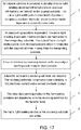
- the present invention further provides a flow diagram of a method for manufacturing a micro light-emitting-diode display panel, which comprises: Step 1, an original substrate 1 is provided. A plurality of micro light-emitting-diode semi-finished products 100 disposed alternatively are formed on the original substrate 1.
- Each of the plurality of micro light-emitting-diode semi-products comprises 100: an LED semi-conductor layer 2 disposed on the original substrate 1, a first insulating layer 3 covering the LED semi-conductor layer 2 and the original substrate 1, a bottom electrode 6 disposed on the first insulating layer 3 and contacted with the LED semi-conductor layer 2, and a connection electrode 7 disposed on the first insulating layer 3 and contacted with the original substrate 1.
- the step S1 specifically comprises: Step 11, please refer to Fig. 1 , an original substrate 1 is provided. An LED semi-conductor thin film 2' is formed on the original substrate 1. A patterned first photoresist layer 10 is formed on the LED semi-conductor thin film 2'.
- Step 12 please refer to Fig. 2 , the LED semi-conductor thin film 2' is etched with the first photoresist layer 10 as a shielding, to form a plurality of LED semi-conductor layers 2 with an interval arrangement.
- Step 13 please refer to Figs. 3 and 4 , a first insulating layer 3 is covered on the LED semi-conductor layers 2 and the original substrate1. A patterned second photoresist layer 20 is formed on the first insulating layer 3.
- Step 14 please refer to Fig. 5 , the first insulating layer 3 is etched with the second photoresist layer 20 as a shielding, to form a first via 4 and a second via 5, penetrating through the first insulating layer 3.
- the first via 4 and the second via 5 respectively reveals a portion of the LED semiconductor layers 2 and a portion of the original substrate 1.
- Step 15 please refer to Figs. 6 and 7 , a first metal thin film 6' is formed on the first insulating layer 3, the LED semi-conductor layer 2, and the original substrate 1.
- a patterned third photoresist layer 30 is formed on the first metal thin film 6'.
- Step 16 please refer to Fig. 8 , the first metal thin film 6' is etched with the third photoresist layer 30 as a shielding, to form a bottom electrode 6 and a connection electrode 7.
- the bottom electrode 6 contact with the LED semi-conductor layer 2 through the first via 4.
- the connection electrode 8 contact with the original substrate 1 through the second via 5.
- the original substrate 1 is a sapphire substrate (Al 2 O 3 ), a silicon substrate (Si), a silicon carbide substrate (SiC), or a gallium nitride substrate (GaN), and the like.
- the LED semiconductor layer 2 includes an N+ layer, a P+ layer and a multi-quantum well layer in contact with the N+ and P+ layers.
- the material of the bottom electrode 6 and the connection electrode 7 may be a combination of one or more of metals such as nickel, molybdenum, aluminum, gold, platinum, and titanium.
- the material of the first insulating layer 3 is silicon oxide, silicon nitride, or alumina and the like.
- Step 2 a transporting substrate 8 is provided. A surface of the transporting substrate 8 is bonded to the bottom electrode 6 and the connection electrode 7 of each of the micro emitting diode semi-finished products 100.
- the original substrate 1 is peeled off, to transfer all of the micro emitting diode semi-finished products 100 to the transporting substrate 8 and to expose a side surface of the LED semi-conductor layer 2 contacted with the original substrate 1.
- the transporting substrate 8 in the step 2 is a hard substrate having an adhesive layer on its surface. With the adhesive layer on the surface of the hard substrate to adhere the bottom electrode 6 and the connection electrode 7, the micro emitting diode semi-finished products 100 and the transporting substrate 8 are adhered,.
- the original substrate 1 is peeled off with a Laser lift-off (LLO) technology, to transfer the micro emitting diode semi-finished products 100 to the transporting substrate 8 and to expose the side surface of the LED semi-conductor layer 2 contacted with the original substrate 1.
- LLO Laser lift-off
- the step 2 further comprises: the transporting substrate 8 and the semi-finished product 100 of the micro-emitter diode on the transporting substrate 8 are reversed, so that the exposed side of the LED semiconductor layer 2 faces upwards, facilitating the subsequent process.
- Step 3 a second insulating layer 9 and a top electrode 13 disposed on the second insulating layer 9 are orderly formed on the exposed LED semi-conductor layer 2 and the first insulating layer 3, to obtain a plurality of micro light-emitting-diodes 200 with an interval arrangement.
- the top electrode 13 is contacted with the LED semi-conductor layer 2 and the connection electrode 7.
- the first insulating layer 3 and the second insulating layer 9 together constitute an insulation-protective layer 14 surrounding the LED semiconductor layer 2.
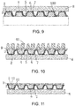
- step S3 specifically comprises: step 31, please refer to Fig. 10 , a second insulating layer 9 is formed on the LED semi-conductor layer 2 and the first insulating layer 3. A patterned fourth photoresist layer 40 is formed on the second insulating layer 9.
- Step 32 please refer to Fig. 11 , the second insulating layer 9 is etched with the fourth photoresist layer 40 as a shielding, to form a third via 11 and a fourth via 12, penetrating through the second insulating layer 9.
- the third via 11 and the fourth via 12 respectively reveals a portion of the LED semi-conductor layer 2 and a portion of the connection electrode 7.
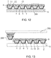
- Step 33 please refer to Fig. 12 , a conductive thin film is deposited and patterned on the second insulating layer 9, to form a top electrode 13.
- the top electrode 13 contacts with the LED semi-conductor layer 2 and the connection electrode 7 through the third via 11 and the fourth via 12, respectively.
- the receiving substrate 400 comprises: a base substrate 41, a plurality of sub-pixel regions 15 disposing on the base substrate 41 in an array arrangement, and first electrode contact 43 and second electrode contact 44 alternatively disposing within each of the sub-pixel regions 15.
- the receiving substrate 400 provided in the step S4 further comprises: a TFT layer 42 and a pixel definition layer 45.
- the TFT layer 42 is disposed between the base substrate 41, and the first electrode contact 43 and the second electrode contact 44.
- the TFT layer 42 comprises: an active layer 421 disposed on the base substrate 41, a gate insulating layer 422 covering the active layer 421 and the base substrate 41, a gate electrode 423 disposed on the gate insulating layer 422 above the active layer 421, an intermediate insulating layer 424 covering the gate electrode 423 and the gate insulating layer 422, a source electrode 425 and a drain electrode 426 disposing on the intermediate insulating layer 424 and contacting with two ends of the active layer 421, and a passivation layer 427 covering the source electrode 425, the drain electrode 426 and the intermediate insulating layer 424.
- the second electrode contact 44 contact with the source electrode 425.
- the pixel definition layer 45 is disposed on the passivation layer 427 and located around the micro light-
- Step 5 please refer to Fig. 14 , the micro light-emitting-diodes 200 on the transporting substrate 8 are transferred onto the receiving substrate 400 by the transfer head 300.
- Each of the sub-pixel regions 15 corresponds to the micro light-emitting-diodes 200.
- the bottom electrode 6 and the connection electrode 7 of the micro light-emitting-diodes 200 of each of the sub-pixel regions 15 are respectively bonded to the first electrode contact 43 and the second electrode contact 44 within the sub-pixel region 15.
- Step 6 a test voltage is provided to the first electrode contact 43 and the second electrode contact 44 to test whether the respective micro light-emitting-diodes 200 on the receiving substrate 400 are normally lit or not. If all of the micro light-emitting-diodes 200 on the receiving substrate 400 are normally lit, a protective layer 16 is continuously formed on the micro light-emitting-diodes 200, the passivation layer 427, the pixel definition layer 45, the first electrode contact 43, and the second electrode contact 44.
- micro light-emitting-diodes 200 on the receiving substrate 400 are not normally lit, the micro light-emitting-diodes 200 which are not normally lit are replaced with new micro light-emitting-diodes 200. All of the micro light-emitting-diodes 200 on the receiving substrate 400 are re-tested until they are normally lit.
- the protective layer 16 has a function of enhancing the light extraction of the micro light-emitting-diodes 200, and the protective layer 16 has a good heat transfer capability.
- the micro-light emitting diode display panel of the present invention firstly manufactures a semi-finished product 100 including a bottom electrode 6, an LED semiconductor layer 2, and a micro-light-emitting-diode connecting the electrode 7 on the original substrate 1, then, the semi-finished product 100 is transferred onto the transport substrate 8 and is inverted upside down, and then the top electrode 13 connected to both the LED semiconductor layer 2 and the connection electrode 7 is formed to obtain the micro light-emitting-diodes 200, and finally the micro light-emitting-diodes 200 is transferred onto the receiving substrate 400 so that the bottom electrode 6 and the connection electrode 7 are in contact with the first electrode contact 43 and the second electrode contact 44, respectively, so that after the micro light-emitting-diodes 200 are transferred, without any process, the lighting test of the light-emitting-diodes 200 can immediately be performed, and other structures such as the protective layer 16 can be continuously manufactured after the micro light-emitting-diodes 200 are determined as normally lit,
- the present invention provides a micro light-emitting-diode display panel.
- a first electrode contact and a second electrode contact are disposed alternatively on a base substrate of the micro light-emitting-diodes display panel.
- the first electrode contact and the second electrode contact are respectively in contact with the bottom electrode and the connection electrode of the micro light-emitting-diodes.
- the connection electrode is also in contact with the top electrode of the micro light-emitting-diodes, and the micro light-emitting-diodes can be immediately detected after the micro light-emitting-diodes are transferred, to reduce the difficulty of product detection and product repair, and to improve the product yield.
Landscapes
- Devices For Indicating Variable Information By Combining Individual Elements (AREA)
- Led Device Packages (AREA)
- Engineering & Computer Science (AREA)
- Manufacturing & Machinery (AREA)
- Led Devices (AREA)
Abstract
Description
- The present invention relates to the field of liquid crystal display, and more particularly to a micro light-emitting-diode display panel and a manufacturing method thereof.
- Because of the advantages of high quality, power saving, thin body and wide applications, the flat panel display devices has become a mainstream in the display devices and been widely used in various consumer electronic devices, such as mobile phones, personal digital assistants, digital cameras, laptops, and desktop computers.
- A micro LED display is a display that achieves image display by using a high density and small size LED arrays integrated on a substrate as display pixels, the same as the large-size outdoor LED display, each pixel can be addressed, be individually driven to light, can be seen as a shrink-down version of the outdoor LED display, to reduce the pixel distance from millimeter to micron. The Micro LED display and the organic light-emitting-diode (OLED) display are belong to self-luminous displays, however, with comparing with OLED display, the Micro LED display has better material stability, longer life, no image mark, etc., which is considered the biggest competitor of the OLED display.
- In the manufacturing process of the micro LED display panel, the micro light-emitting-diodes must grow on an original substrate (such as sapphire-type substrate) by the molecular beam epitaxy method, for making the display panel, the micro light-emitting-diode devices should be transferred from the original substrate to a receiving substrate for forming the display panel in a display arrangement. Specifically, the micro light-emitting-diodes are firstly formed on the original substrate, then, the micro light-emitting-diodes are lifted from the original substrate by a laser lift-off (LLO) technology, the micro light-emitting-diodes are adhered from the original substrate to preset positions of the receiving substrate, by using a transfer head which is made of a material such as polydimethylsiloxane (PDMS).
- Presently, after the micro light-emitting-diodes are transferred to the receiving substrate, but also a top electrode needs to be formed to determine whether the bonding between the micro light-emitting-diodes and receiving substrate is normal or not. However, because the process has been basically completed at this moment, in this case even if the bonding between the micro light-emitting-diodes and the receiving substrate is poor, it is difficult to repair. Hence, it is needed to provide a new micro LED display panel and a manufacturing method thereof, which is capable of immediately performing the work-condition test of the micro light-emitting-diodes after transferring, to reduce the difficulty of product detection and product repair, and to improve the product yield.
- An object of the present invention is to provide a micro light-emitting-diode display panel, which can reduce the difficulty of product detection and product repair and improve product yield.
- An object of the present invention is to further provide a manufacturing for a micro light-emitting-diode display panel, which can reduce the difficulty of product detection and product repair and improve product yield.
- In order to achieve the objective, the present invention provides a micro light-emitting-diode display panel, which comprises: a base substrate, a plurality of sub-pixel regions disposing with an array arrangement on the base substrate, a first electrode contact and a second electrode contact alternatively disposing within each of the sub-pixel regions, and a micro light-emitting-diode disposing on the first electrode contact and the second electrode contact within each of the sub-pixel regions.
- The micro light-emitting-diode comprises: a bottom electrode contacting with the first electrode contact, an LED semiconductor layer disposing above the bottom electrode and contacting with the bottom electrode, a top electrode disposing on the LED semiconductor layer and contacting with the LED semiconductor layer, an insulation-protective layer surrounding the LED semiconductor layer, and a connection electrode disposing on the insulation-protective layer and connecting with the top electrode and the second electrode contact.
- The micro light-emitting-diode display panel further comprises: a TFT layer is disposed between the base substrate, and the first electrode contact and the second electrode contact.
- The TFT layer comprises: an active layer disposed on the base substrate, a gate insulating layer covering the active layer and the base substrate, a gate electrode disposed on the gate insulating layer above the active layer, an intermediate insulating layer covering the gate electrode and the gate insulating layer, a source electrode and a drain electrode disposing on the intermediate insulating layer and contacting with two ends of the active layer, and a passivation layer covering the source electrode, the drain electrode and the intermediate insulating layer. The second electrode contact contacts with the source electrode.
- The micro light-emitting-diode display panel further comprises: a pixel definition layer disposed on the passivation layer and located around the micro light-emitting-diode, and a protective layer covering the passivation layer, the first electrode contact, the second electrode contact, the micro light-emitting-diode, and the pixel definition layer.
- The present invention further provides a method for manufacturing a micro light-emitting-diode display panel, which comprises:
Step 1, an original substrate is provided. A plurality of micro light-emitting-diode semi-finished products disposed alternatively are formed on the original substrate. - Each of the plurality of micro light-emitting-diode semi-products comprises: an LED semi-conductor layer disposed on the original substrate, a first insulating layer covering the LED semi-conductor layer and the original substrate, a bottom electrode disposed on the first insulating layer and contacted with the LED semi-conductor layer, and a connection electrode disposed on the first insulating layer and contacted with the original substrate.
-
Step 2, a transporting substrate is provided. A surface of the transporting substrate is bonded to the bottom electrode and the connection electrode of each of the micro emitting diode semi-finished products. The original substrate is peeled off, to transfer all of the micro emitting diode semi-finished products to the transporting substrate and to expose a side surface of the LED semi-conductor layer contacted with the original substrate. -
Step 3, a second insulating layer and a top electrode disposed on the second insulating layer are orderly formed on the exposed LED semi-conductor layer and the first insulating layer, to obtain a plurality of micro light-emitting-diodes with an interval arrangement. The top electrode is contacted with the LED semi-conductor layer and the connection electrode. -
Step 4, a transfer head and a receiving substrate are provided. The receiving substrate comprises: a base substrate, a plurality of sub-pixel regions disposing on the base substrate in an array arrangement, and a first electrode contact and a second electrode contact alternatively disposing within each of the sub-pixel regions. -
Step 5, the micro light-emitting-diodes on the transporting substrate are transferred onto the receiving substrate by the transfer head. Each of the sub-pixel regions corresponds to the micro light-emitting-diodes. The bottom electrode and the connection electrode of the micro light-emitting-diodes of each of the sub-pixel regions are respectively bonded to the first electrode contact and the second electrode contact within the sub-pixel region. -
Step 6, a test voltage is provided to the first electrode contact and the second electrode contact to test whether the respective micro light-emitting-diodes on the receiving substrate are normally lit or not. If all of the micro light-emitting-diodes on the receiving substrate are normally lit, a protective layer is continuously formed on the micro light-emitting-diodes, the first electrode contact, and the second electrode contact. If the micro light-emitting-diodes on the receiving substrate are not normally lit, the micro light-emitting-diodes which are not normally lit are replaced with new micro light-emitting-diodes. All of the micro light-emitting-diodes on the receiving substrate are re-tested until they are normally lit. - The step S1 specifically comprises:
Step 11, an original substrate is provided. An LED semi-conductor thin film is formed on the original substrate. A patterned first photoresist layer is formed on the LED semi-conductor thin film. -
Step 12, the LED semi-conductor thin film is etched with the first photoresist layer as a shielding, to form a plurality of LED semi-conductor layers with an interval arrangement. -
Step 13, a first insulating layer is covered on the LED semi-conductor layers and the original substrate. A patterned second photoresist layer is formed on the first insulating layer. -
Step 14, the first insulating layer is etched with the second photoresist layer as a shielding, to form a first via and a second via, penetrating through the first insulating layer. The first via and the second via respectively reveals a portion of the LED semiconductor layers and a portion of the original substrate. -
Step 15, a first metal thin film is formed on the first insulating layer, the LED semi-conductor layer, and the original substrate. A patterned third photoresist layer is formed on the first metal thin film. -
Step 16, the first metal thin film is etched with the third photoresist layer as a shielding, to form a bottom electrode and a connection electrode. The bottom electrode contact with the LED semi-conductor layer through the first via. The connection electrode contact with the original substrate through the second via. - The transporting substrate in the
step 2 is a hard substrate having an adhesive layer on its surface. - The
step 3 specifically comprises:
Step 31, a second insulating layer is formed on the LED semi-conductor layer and the first insulating layer. A patterned fourth photoresist layer is formed on the second insulating layer. - Step 32, the second insulating layer is etched with the fourth photoresist layer as a shielding, to form a third via and a fourth via, penetrating through the second insulating layer. The third via and the fourth via respectively reveals a portion of the LED semi-conductor layer and a portion of the connection electrode.
- Step 33, a conductive thin film is deposited and patterned on the second insulating layer, to form a top electrode. The top electrode contact with the LED semi-conductor layer and the connection electrode through the third via and the fourth via, respectively.
- The receiving substrate provided in the step S4 further comprises: a TFT layer and a pixel definition layer.
- The TFT layer is disposed between the base substrate, and the first electrode contact and the second electrode contact. The TFT layer comprises: an active layer disposed on the base substrate, a gate insulating layer covering the active layer and the base substrate, a gate electrode disposed on the gate insulating layer above the active layer, an intermediate insulating layer covering the gate electrode and the gate insulating layer, a source electrode and a drain electrode disposing on the intermediate insulating layer and contacting with two ends of the active layer, and a passivation layer covering the source electrode, the drain electrode and the intermediate insulating layer; the second electrode contact contacts with the source electrode. The pixel definition layer is disposed on the passivation layer and located around the micro light-emitting-diodes.
- At least two bonding positions are preset on the first electrode contact and the second electrode contact. When the micro light-emitting-diodes which are not normally lit, are replaced with the new micro light-emitting-diodes in the
step 6, the micro light-emitting-diodes after a replacement and the micro light-emitting-diodes before replacement are in different bonding positions. - The original substrate is peeled off by a laser stripping process in
step 2. - The present invention further provides a method for manufacturing a micro light-emitting-diode display panel, which comprises:
Step 1, an original substrate is provided. A plurality of micro light-emitting-diode semi-finished products disposed alternatively are formed on the original substrate. - Each of the plurality of micro light-emitting-diode semi-products comprises: an LED semi-conductor layer disposed on the original substrate, a first insulating layer covering the LED semi-conductor layer and the original substrate, a bottom electrode disposed on the first insulating layer and contacted with the LED semi-conductor layer, and a connection electrode disposed on the first insulating layer and contacted with the original substrate.
-
Step 2, a transporting substrate is provided. A surface of the transporting substrate is bonded to the bottom electrode and the connection electrode of each of the micro emitting diode semi-finished products. The original substrate is peeled off, to transfer all of the micro emitting diode semi-finished products to the transporting substrate and to expose a side surface of the LED semi-conductor layer contacted with the original substrate. -
Step 3, a second insulating layer and a top electrode disposed on the second insulating layer are orderly formed on the exposed LED semi-conductor layer and the first insulating layer, to obtain a plurality of micro light-emitting-diodes with an interval arrangement. The top electrode is contacted with the LED semi-conductor layer and the connection electrode. -
Step 4, a transfer head and a receiving substrate are provided. The receiving substrate comprises: a base substrate, a plurality of sub-pixel regions disposing on the base substrate in an array arrangement, and a first electrode contact and a second electrode contact alternatively disposing within each of the sub-pixel regions. -
Step 5, the micro light-emitting-diodes on the transporting substrate are transferred onto the receiving substrate by the transfer head. Each of the sub-pixel regions corresponds to the micro light-emitting-diodes. The bottom electrode and the connection electrode of the micro light-emitting-diodes of each of the sub-pixel regions are respectively bonded to the first electrode contact and the second electrode contact within the sub-pixel region. -
Step 6, a test voltage is provided to the first electrode contact and the second electrode contact to test whether the respective micro light-emitting-diodes on the receiving substrate are normally lit or not. If all of the micro light-emitting-diodes on the receiving substrate are normally lit, a protective layer is continuously formed on the micro light-emitting-diodes, the first electrode contact, and the second electrode contact. If the micro light-emitting-diodes on the receiving substrate are not normally lit, the micro light-emitting-diodes which are not normally lit are replaced with new micro light-emitting-diodes. All of the micro light-emitting-diodes on the receiving substrate are re-tested until they are normally lit. - Wherein the step S1 specifically comprises:
Step 11, an original substrate is provided. An LED semi-conductor thin film is formed on the original substrate. A patterned first photoresist layer is formed on the LED semi-conductor thin film. -
Step 12, the LED semi-conductor thin film is etched with the first photoresist layer as a shielding, to form a plurality of LED semi-conductor layers with an interval arrangement. -
Step 13, a first insulating layer is covered on the LED semi-conductor layers and the original substrate. A patterned second photoresist layer is formed on the first insulating layer. -
Step 14, the first insulating layer is etched with the second photoresist layer as a shielding, to form a first via and a second via, penetrating through the first insulating layer. The first via and the second via respectively reveals a portion of the LED semiconductor layers and a portion of the original substrate. -
Step 15, a first metal thin film is formed on the first insulating layer, the LED semi-conductor layer, and the original substrate. A patterned third photoresist layer is formed on the first metal thin film. -
Step 16, the first metal thin film is etched with the third photoresist layer as a shielding, to form a bottom electrode and a connection electrode. The bottom electrode contact with the LED semi-conductor layer through the first via. The connection electrode contact with the original substrate through the second via. - Wherein the transporting substrate in the
step 2 is a hard substrate having an adhesive layer on its surface. - The beneficial effects of the present invention is: the present invention provides a micro light-emitting-diode display panel. A first electrode contact and a second electrode contact are disposed alternatively on a base substrate of the micro light-emitting-diodes display panel. The first electrode contact and the second electrode contact are respectively in contact with the bottom electrode and the connection electrode of the micro light-emitting-diodes. The connection electrode is also in contact with the top electrode of the micro light-emitting-diodes, and the micro light-emitting-diodes can be immediately detected after the micro light-emitting-diodes are transferred, to reduce the difficulty of product detection and product repair, and to improve the product yield. The invention also provides a method for manufacturing a micro light-emitting-diode display panel, which is capable of immediately detecting the micro light-emitting-diodes after the micro light-emitting-diodes are transferred, to reduce the difficulty of product detection and product repair, and to improve the product yield.
- For better understanding the technical proposals and other beneficial effects of the present invention, please refer the following detailed description of the present invention with the accompanying drawings.
- In drawings:
-
Figs. 1-8 are illustrative diagrams of the step S1 of a method for manufacturing a micro light-emitting-diode display panel according to the present invention. -
Fig. 9 is illustrative diagram of the step S2 of a method for manufacturing a micro light-emitting-diode display panel according to the present invention. -
Figs. 10-12 are illustrative diagrams of the step S3 of a method for manufacturing a micro light-emitting-diode display panel according to the present invention. -
Figs. 13 and14 are illustrative diagrams of the step S4 and the step S5 of a method for manufacturing a micro light-emitting-diode display panel according to the present invention. -
Figs. 15 is illustrative diagram of the step S6 of a method for manufacturing a micro light-emitting-diode display panel according to the present invention and also a structural illustrative diagram of the micro light-emitting-diode display panel according to the present invention. -
Fig. 16 is top-view illustration of the step S6 of a method for manufacturing a micro light-emitting-diode display panel according to the present invention. -
Fig. 17 is a flow diagram of a method for manufacturing a micro light-emitting-diode display panel according to the present invention. - The technical proposals and the effects of the present invention will be described in further detail with reference to the below preferred embodiments of the present invention and their accompanying drawings.
- Please refer to
Fig. 15 , the present invention provides a micro light-emitting-diode display panel, which comprises: abase substrate 41, a plurality ofsub-pixel regions 15 disposing with an array arrangement on thebase substrate 41, afirst electrode contact 43 and asecond electrode contact 44 alternatively disposing within each of thesub-pixel regions 15, and a micro light-emitting-diode 200 disposing on thefirst electrode contact 43 and thesecond electrode contact 44 within each of thesub-pixel regions 15. - The micro light-emitting-
diode 200 comprises: abottom electrode 6 contacting with thefirst electrode contact 43, anLED semiconductor layer 2 disposing above thebottom electrode 6 and contacting with thebottom electrode 6, atop electrode 13 disposing on theLED semiconductor layer 2 and contacting with theLED semiconductor layer 2, an insulation-protective layer 14 surrounding theLED semiconductor layer 2, and aconnection electrode 7 disposing on the insulation-protective layer 14 and connecting with thetop electrode 13 and thesecond electrode contact 44. - Specifically, the micro light-emitting-diode display panel further comprises: a
TFT layer 42 is disposed between thebase substrate 41, and thefirst electrode contact 43 and thesecond electrode contact 44. TheTFT layer 42 comprises: anactive layer 421 disposed on thebase substrate 41, agate insulating layer 422 covering theactive layer 421 and thebase substrate 41, agate electrode 423 disposed on thegate insulating layer 422 above theactive layer 421, an intermediate insulatinglayer 424 covering thegate electrode 423 and thegate insulating layer 422, asource electrode 425 and adrain electrode 426 disposing on the intermediate insulatinglayer 424 and contacting with two ends of theactive layer 421, and apassivation layer 427 covering thesource electrode 425 , thedrain electrode 426 and the intermediate insulatinglayer 424. Thesecond electrode contact 44 contact with thesource electrode 425. - Specifically, the micro light-emitting-diode display panel further comprises: a
pixel definition layer 45 disposed on thepassivation layer 427 and located around the micro light-emitting-diode 200, and aprotective layer 16 covering thepassivation layer 427, thefirst electrode contact 43, thesecond electrode contact 44, the micro light-emitting-diode 200, and thepixel definition layer 45. - Specifically, the
protective layer 16 has a function of enhancing the light extraction of the micro light-emitting-diode 200, and theprotective layer 16 has a good heat transfer capability. - Specifically, the
LED semiconductor layer 2 comprises an N+ layer, a P+ layer, and a multi-quantum well layer in contact with the N+ layer and the P+ layer. The material of thebottom electrode 6 and theconnection electrode 7 may be selected from at least one of nickel (Ni), molybdenum (Mo), aluminum (Al), gold (Au), platinum (Pt), and titanium (Ti). Thetop electrode 13 is a transparent electrode, which is made from indium tin oxide (ITO), indium zinc oxide (IZO), or a mixture of polyethylene dioxythiophene and polystyrene sulfonic acid (PEDOT: PSS). The insulation-protective layer 14 is made from silicon oxide (SiOx), silicon nitride (SiNx), or alumina (Al2O3). - It is to be noted that, with that the
top electrode 13 and thesecond electrode contact 44 are connected by theconnection electrode 7 in the micro light-emitting-diode display panel of the present invention, thetop electrode 13 can be immediately formed before the micro light-emitting-diodes are transferred, the micro light-emitting-diodes 200 can directly perform the lighting test of the micro light-emitting-diodes 200 after the micro light-emitting-diodes 200 is transferred, and when the micro light-emitting-diodes 200 are determined as being normal lit, and then continues to manufacture other structures such as theprotective layer 16, which is capable of reducing the difficulty of product detection and product repair, and improving the product yield. - Please refer to
Fig. 17 , the present invention further provides a flow diagram of a method for manufacturing a micro light-emitting-diode display panel, which comprises:
Step 1, anoriginal substrate 1 is provided. A plurality of micro light-emitting-diodesemi-finished products 100 disposed alternatively are formed on theoriginal substrate 1. - Each of the plurality of micro light-emitting-diode semi-products comprises 100: an
LED semi-conductor layer 2 disposed on theoriginal substrate 1, a first insulatinglayer 3 covering theLED semi-conductor layer 2 and theoriginal substrate 1, abottom electrode 6 disposed on the first insulatinglayer 3 and contacted with theLED semi-conductor layer 2, and aconnection electrode 7 disposed on the first insulatinglayer 3 and contacted with theoriginal substrate 1. - Specifically, the step S1 specifically comprises:
Step 11, please refer toFig. 1 , anoriginal substrate 1 is provided. An LED semi-conductor thin film 2' is formed on theoriginal substrate 1. A patternedfirst photoresist layer 10 is formed on the LED semi-conductor thin film 2'. -
Step 12, please refer toFig. 2 , the LED semi-conductor thin film 2' is etched with thefirst photoresist layer 10 as a shielding, to form a plurality of LEDsemi-conductor layers 2 with an interval arrangement. -
Step 13, please refer toFigs. 3 and 4 , a first insulatinglayer 3 is covered on the LEDsemi-conductor layers 2 and the original substrate1. A patternedsecond photoresist layer 20 is formed on the first insulatinglayer 3. -
Step 14, please refer toFig. 5 , the first insulatinglayer 3 is etched with thesecond photoresist layer 20 as a shielding, to form a first via 4 and a second via 5, penetrating through the first insulatinglayer 3. The first via 4 and the second via 5 respectively reveals a portion of theLED semiconductor layers 2 and a portion of theoriginal substrate 1. -
Step 15, please refer toFigs. 6 and 7 , a first metal thin film 6' is formed on the first insulatinglayer 3, theLED semi-conductor layer 2, and theoriginal substrate 1. A patternedthird photoresist layer 30 is formed on the first metal thin film 6'. -
Step 16, please refer toFig. 8 , the first metal thin film 6' is etched with thethird photoresist layer 30 as a shielding, to form abottom electrode 6 and aconnection electrode 7. Thebottom electrode 6 contact with theLED semi-conductor layer 2 through the first via 4. Theconnection electrode 8 contact with theoriginal substrate 1 through the second via 5. - Specifically, the
original substrate 1 is a sapphire substrate (Al2O3), a silicon substrate (Si), a silicon carbide substrate (SiC), or a gallium nitride substrate (GaN), and the like. TheLED semiconductor layer 2 includes an N+ layer, a P+ layer and a multi-quantum well layer in contact with the N+ and P+ layers. The material of thebottom electrode 6 and theconnection electrode 7 may be a combination of one or more of metals such as nickel, molybdenum, aluminum, gold, platinum, and titanium. The material of the first insulatinglayer 3 is silicon oxide, silicon nitride, or alumina and the like. -
Step 2, a transportingsubstrate 8 is provided. A surface of the transportingsubstrate 8 is bonded to thebottom electrode 6 and theconnection electrode 7 of each of the micro emitting diodesemi-finished products 100. Theoriginal substrate 1 is peeled off, to transfer all of the micro emitting diodesemi-finished products 100 to the transportingsubstrate 8 and to expose a side surface of theLED semi-conductor layer 2 contacted with theoriginal substrate 1. - Specifically, the transporting
substrate 8 in thestep 2 is a hard substrate having an adhesive layer on its surface. With the adhesive layer on the surface of the hard substrate to adhere thebottom electrode 6 and theconnection electrode 7, the micro emitting diodesemi-finished products 100 and the transportingsubstrate 8 are adhered,. Theoriginal substrate 1 is peeled off with a Laser lift-off (LLO) technology, to transfer the micro emitting diodesemi-finished products 100 to the transportingsubstrate 8 and to expose the side surface of theLED semi-conductor layer 2 contacted with theoriginal substrate 1. - Specifically, the
step 2 further comprises: the transportingsubstrate 8 and thesemi-finished product 100 of the micro-emitter diode on the transportingsubstrate 8 are reversed, so that the exposed side of theLED semiconductor layer 2 faces upwards, facilitating the subsequent process. -
Step 3, a secondinsulating layer 9 and atop electrode 13 disposed on the second insulatinglayer 9 are orderly formed on the exposedLED semi-conductor layer 2 and the first insulatinglayer 3, to obtain a plurality of micro light-emitting-diodes 200 with an interval arrangement. Thetop electrode 13 is contacted with theLED semi-conductor layer 2 and theconnection electrode 7. - Specifically, the first insulating
layer 3 and the second insulatinglayer 9 together constitute an insulation-protective layer 14 surrounding theLED semiconductor layer 2. - Specifically, the step S3 specifically comprises: step 31, please refer to
Fig. 10 , a secondinsulating layer 9 is formed on theLED semi-conductor layer 2 and the first insulatinglayer 3. A patternedfourth photoresist layer 40 is formed on the second insulatinglayer 9. - Step 32, please refer to
Fig. 11 , the second insulatinglayer 9 is etched with thefourth photoresist layer 40 as a shielding, to form a third via 11 and a fourth via 12, penetrating through the second insulatinglayer 9. The third via 11 and the fourth via 12 respectively reveals a portion of theLED semi-conductor layer 2 and a portion of theconnection electrode 7. - Step 33, please refer to
Fig. 12 , a conductive thin film is deposited and patterned on the second insulatinglayer 9, to form atop electrode 13. Thetop electrode 13 contacts with theLED semi-conductor layer 2 and theconnection electrode 7 through the third via 11 and the fourth via 12, respectively. -
Step 4, please refer toFigs. 13 and14 , atransfer head 300 and a receivingsubstrate 400 are provided. The receivingsubstrate 400 comprises: abase substrate 41, a plurality ofsub-pixel regions 15 disposing on thebase substrate 41 in an array arrangement, andfirst electrode contact 43 andsecond electrode contact 44 alternatively disposing within each of thesub-pixel regions 15. - Specifically, the receiving
substrate 400 provided in the step S4 further comprises: aTFT layer 42 and apixel definition layer 45. TheTFT layer 42 is disposed between thebase substrate 41, and thefirst electrode contact 43 and thesecond electrode contact 44. theTFT layer 42 comprises: anactive layer 421 disposed on thebase substrate 41, agate insulating layer 422 covering theactive layer 421 and thebase substrate 41, agate electrode 423 disposed on thegate insulating layer 422 above theactive layer 421, an intermediate insulatinglayer 424 covering thegate electrode 423 and thegate insulating layer 422, asource electrode 425 and adrain electrode 426 disposing on the intermediate insulatinglayer 424 and contacting with two ends of theactive layer 421, and apassivation layer 427 covering thesource electrode 425, thedrain electrode 426 and the intermediate insulatinglayer 424. Thesecond electrode contact 44 contact with thesource electrode 425. Thepixel definition layer 45 is disposed on thepassivation layer 427 and located around the micro light-emitting-diodes 200. -
Step 5, please refer toFig. 14 , the micro light-emitting-diodes 200 on the transportingsubstrate 8 are transferred onto the receivingsubstrate 400 by thetransfer head 300. Each of thesub-pixel regions 15 corresponds to the micro light-emitting-diodes 200. Thebottom electrode 6 and theconnection electrode 7 of the micro light-emitting-diodes 200 of each of thesub-pixel regions 15 are respectively bonded to thefirst electrode contact 43 and thesecond electrode contact 44 within thesub-pixel region 15. -
Step 6, please refer toFigs. 15 and16 , a test voltage is provided to thefirst electrode contact 43 and thesecond electrode contact 44 to test whether the respective micro light-emitting-diodes 200 on the receivingsubstrate 400 are normally lit or not. If all of the micro light-emitting-diodes 200 on the receivingsubstrate 400 are normally lit, aprotective layer 16 is continuously formed on the micro light-emitting-diodes 200, thepassivation layer 427, thepixel definition layer 45, thefirst electrode contact 43, and thesecond electrode contact 44. If the micro light-emitting-diodes 200 on the receivingsubstrate 400 are not normally lit, the micro light-emitting-diodes 200 which are not normally lit are replaced with new micro light-emitting-diodes 200. All of the micro light-emitting-diodes 200 on the receivingsubstrate 400 are re-tested until they are normally lit. - Specifically, the
protective layer 16 has a function of enhancing the light extraction of the micro light-emitting-diodes 200, and theprotective layer 16 has a good heat transfer capability. - It is to be noted that the micro-light emitting diode display panel of the present invention firstly manufactures a
semi-finished product 100 including abottom electrode 6, anLED semiconductor layer 2, and a micro-light-emitting-diode connecting theelectrode 7 on theoriginal substrate 1, then, thesemi-finished product 100 is transferred onto thetransport substrate 8 and is inverted upside down, and then thetop electrode 13 connected to both theLED semiconductor layer 2 and theconnection electrode 7 is formed to obtain the micro light-emitting-diodes 200, and finally the micro light-emitting-diodes 200 is transferred onto the receivingsubstrate 400 so that thebottom electrode 6 and theconnection electrode 7 are in contact with thefirst electrode contact 43 and thesecond electrode contact 44, respectively, so that after the micro light-emitting-diodes 200 are transferred, without any process, the lighting test of the light-emitting-diodes 200 can immediately be performed, and other structures such as theprotective layer 16 can be continuously manufactured after the micro light-emitting-diodes 200 are determined as normally lit, thereby reducing the difficulty of detection and product repair, and improving the product yield. - As mentioned above, the present invention provides a micro light-emitting-diode display panel. A first electrode contact and a second electrode contact are disposed alternatively on a base substrate of the micro light-emitting-diodes display panel. The first electrode contact and the second electrode contact are respectively in contact with the bottom electrode and the connection electrode of the micro light-emitting-diodes. The connection electrode is also in contact with the top electrode of the micro light-emitting-diodes, and the micro light-emitting-diodes can be immediately detected after the micro light-emitting-diodes are transferred, to reduce the difficulty of product detection and product repair, and to improve the product yield.
- As mentioned above, those of ordinary skill in the art, without departing from the spirit and scope of the present invention, can make various kinds of modifications and variations to the present invention. Therefore, all such modifications and variations are intended to be included in the protection scope of the appended claims of the present invention.
Claims (15)
- A micro light-emitting-diode display panel, comprising a base substrate, a plurality of sub-pixel regions disposing with an array arrangement on the base substrate, a first electrode contact and a second electrode contact alternatively disposing within each of the sub-pixel regions, and a micro light-emitting-diode disposing on the first electrode contact and the second electrode contact within each of the sub-pixel regions;
the micro light-emitting-diode comprising: a bottom electrode contacting with the first electrode contact, an LED semiconductor layer disposing above the bottom electrode and contacting with the bottom electrode, a top electrode disposing on the LED semiconductor layer and contacting with the LED semiconductor layer, an insulation-protective layer surrounding the LED semiconductor layer, and a connection electrode disposing on the insulation-protective layer and connecting with the top electrode and the second electrode contact. - The micro light-emitting-diode display panel according to claim 1, further comprising: a TFT layer is disposed between the base substrate, and the first electrode contact and the second electrode contact;
the TFT layer comprises: an active layer disposed on the base substrate, a gate insulating layer covering the active layer and the base substrate, a gate electrode disposed on the gate insulating layer above the active layer, an intermediate insulating layer covering the gate electrode and the gate insulating layer, a source electrode and a drain electrode disposing on the intermediate insulating layer and contacting with two ends of the active layer, and a passivation layer covering the source electrode, the drain electrode and the intermediate insulating layer; the second electrode contact contacts with the source electrode. - The micro light-emitting-diode display panel according to claim 2, further comprising: a pixel definition layer disposed on the passivation layer and located around the micro light-emitting-diode, and a protective layer covering the passivation layer, the first electrode contact, the second electrode contact, the micro light-emitting-diode, and the pixel definition layer.
- A method for manufacturing a micro light-emitting-diode display panel, comprising:step 1, providing an original substrate, forming a plurality of micro light-emitting-diode semi-finished products disposed alternatively on the original substrate;
each of the plurality of micro light-emitting-diode semi-products comprising: an LED semi-conductor layer disposed on the original substrate, a first insulating layer covering the LED semi-conductor layer and the original substrate, a bottom electrode disposed on the first insulating layer and contacted with the LED semi-conductor layer, and a connection electrode disposed on the first insulating layer and contacted with the original substrate;step 2, providing a transporting substrate, bonding a surface of the transporting substrate to the bottom electrode and the connection electrode of each of the micro emitting diode semi-finished products, peeling off the original substrate, to transfer all of the micro emitting diode semi-finished products to the transporting substrate and to expose a side surface of the LED semi-conductor layer contacted with the original substrate;step 3, orderly forming a second insulating layer and a top electrode disposed on the second insulating layer on the exposed LED semi-conductor layer and the first insulating layer, to obtain a plurality of micro light-emitting-diodes with an interval arrangement; the top electrode being contacted with the LED semi-conductor layer and the connection electrode;step 4, providing a transfer head and a receiving substrate, the receiving substrate comprising: a base substrate, a plurality of sub-pixel regions disposing on the base substrate in an array arrangement, and a first electrode contact and a second electrode contact alternatively disposing within each of the sub-pixel regions;step 5, transferring the micro light-emitting-diodes on the transporting substrate onto the receiving substrate by the transfer head, each of the sub-pixel regions corresponding to the micro light-emitting-diodes, respectively bonding the bottom electrode and the connection electrode of the micro light-emitting-diodes of each of the sub-pixel regions to the first electrode contact and the second electrode contact within the sub-pixel region;step 6, providing a test voltage to the first electrode contact and the second electrode contact to test whether the respective micro light-emitting-diodes on the receiving substrate are normally lit or not, if all of the micro light-emitting-diodes on the receiving substrate are normally lit, continuously forming a protective layer on the micro light-emitting-diodes, the first electrode contact, and the second electrode contact; if the micro light-emitting-diodes on the receiving substrate are not normally lit, replacing the micro light-emitting-diodes which are not normally lit with new micro light-emitting-diodes, re-testing until all of the micro light-emitting-diodes on the receiving substrate are normally lit. - The method for manufacturing a micro light-emitting-diode display panel according to claim 4, wherein the step S1 specifically comprises:step 11, providing an original substrate, forming an LED semi-conductor thin film on the original substrate, forming a patterned first photoresist layer on the LED semi-conductor thin film;step 12, etching the LED semi-conductor thin film with the first photoresist layer as a shielding, to form a plurality of LED semi-conductor layers with an interval arrangement;step 13, covering a first insulating layer on the LED semi-conductor layers and the original substrate, forming a patterned second photoresist layer on the first insulating layer;step 14, etching the first insulating layer with the second photoresist layer as a shielding, to form a first via and a second via, penetrating through the first insulating layer, the first via and the second via respectively reveals a portion of the LED semiconductor layers and a portion of the original substrate;step 15, forming a first metal thin film on the first insulating layer, the LED semi-conductor layer, and the original substrate, forming a patterned third photoresist layer on the first metal thin film;step 16, etching the first metal thin film with the third photoresist layer as a shielding, to form a bottom electrode and a connection electrode, the bottom electrode contact with the LED semi-conductor layer through the first via, and the connection electrode contact with the original substrate through the second via.
- The method for manufacturing a micro light-emitting-diode display panel according to claim 4, wherein the transporting substrate in the step 2 is a hard substrate having an adhesive layer on its surface.
- The method for manufacturing a micro light-emitting-diode display panel according to claim 4, wherein the step 3 specifically comprises:step 31, forming a second insulating layer on the LED semi-conductor layer and the first insulating layer, forming a patterned fourth photoresist layer on the second insulating layer;step 32, etching the second insulating layer with the fourth photoresist layer as a shielding, to form a third via and a fourth via, penetrating through the second insulating layer, the third via and the fourth via respectively reveals a portion of the LED semi-conductor layer and a portion of the connection electrode;step 33, depositing and patterning a conductive thin film on the second insulating layer, to form a top electrode, the top electrode contact with the LED semi-conductor layer and the connection electrode through the third via and the fourth via, respectively.
- The method for manufacturing a micro light-emitting-diode display panel according to claim 4, wherein the receiving substrate provided in the step S4 further comprises: a TFT layer and a pixel definition layer;
the TFT layer is disposed between the base substrate, and the first electrode contact and the second electrode contact, the TFT layer comprises: an active layer disposed on the base substrate, a gate insulating layer covering the active layer and the base substrate, a gate electrode disposed on the gate insulating layer above the active layer, an intermediate insulating layer covering the gate electrode and the gate insulating layer, a source electrode and a drain electrode disposing on the intermediate insulating layer and contacting with two ends of the active layer, and a passivation layer covering the source electrode, the drain electrode and the intermediate insulating layer; the second electrode contact contacts with the source electrode;
the pixel definition layer is disposed on the passivation layer and located around the micro light-emitting-diodes. - The method for manufacturing a micro light-emitting-diode display panel according to claim 4, wherein at least two bonding positions are preset on the first electrode contact and the second electrode contact, and when the micro light-emitting-diodes which are not be normally lit, are replaced with the new micro light-emitting-diodes in the step 6, the micro light-emitting-diodes after a replacement and the micro light-emitting-diodes before replacement are in different bonding positions.
- The method for manufacturing a micro light-emitting-diode display panel according to claim 4, wherein the original substrate is peeled off by a laser stripping process in step 2.
- A method for manufacturing a micro light-emitting-diode display panel, comprising:step 1, providing an original substrate, forming a plurality of micro light-emitting-diode semi-finished products disposed alternatively on the original substrate;
each of the plurality of micro light-emitting-diode semi-products comprising: an LED semi-conductor layer disposed on the original substrate, a first insulating layer covering the LED semi-conductor layer and the original substrate, a bottom electrode disposed on the first insulating layer and contacted with the LED semi-conductor layer, and a connection electrode disposed on the first insulating layer and contacted with the original substrate;step 2, providing a transporting substrate, bonding a surface of the transporting substrate to the bottom electrode and the connection electrode of each of the micro emitting diode semi-finished products, peeling off the original substrate, to transfer all of the micro emitting diode semi-finished products to the transporting substrate and to expose a side surface of the LED semi-conductor layer contacted with the original substrate;step 3, orderly forming a second insulating layer and a top electrode disposed on the second insulating layer on the exposed LED semi-conductor layer and the first insulating layer, to obtain a plurality of micro light-emitting-diodes with an interval arrangement; the top electrode being contacted with the LED semi-conductor layer and the connection electrode;step 4, providing a transfer head and a receiving substrate, the receiving substrate comprising: a base substrate, a plurality of sub-pixel regions disposing on the base substrate in an array arrangement, and a first electrode contact and a second electrode contact alternatively disposing within each of the sub-pixel regions;step 5, transferring the micro light-emitting-diodes on the transporting substrate onto the receiving substrate by the transfer head, each of the sub-pixel regions corresponding to the micro light-emitting-diodes, respectively bonding the bottom electrode and the connection electrode of the micro light-emitting-diodes of each of the sub-pixel regions to the first electrode contact and the second electrode contact within the sub-pixel region;step 6, providing a test voltage to the first electrode contact and the second electrode contact to test whether the respective micro light-emitting-diodes on the receiving substrate are normally lit or not, if all of the micro light-emitting-diodes on the receiving substrate are normally lit, continuously forming a protective layer on the micro light-emitting-diodes, the first electrode contact, and the second electrode contact; if the micro light-emitting-diodes on the receiving substrate are not normally lit, replacing the micro light-emitting-diodes which are not normally lit with new micro light-emitting-diodes, re-testing until all of the micro light-emitting-diodes on the receiving substrate are normally lit;wherein the step S1 specifically comprises:step 11, providing an original substrate, forming an LED semi-conductor thin film on the original substrate, forming a patterned first photoresist layer on the LED semi-conductor thin film;step 12, etching the LED semi-conductor thin film with the first photoresist layer as a shielding, to form a plurality of LED semi-conductor layers with an interval arrangement;step 13, covering a first insulating layer on the LED semi-conductor layers and the original substrate, forming a patterned second photoresist layer on the first insulating layer;step 14, etching the first insulating layer with the second photoresist layer as a shielding, to form a first via and a second via, penetrating through the first insulating layer, the first via and the second via respectively reveals a portion of the LED semiconductor layers and a portion of the original substrate;step 15, forming a first metal thin film on the first insulating layer, the LED semi-conductor layer, and the original substrate, forming a patterned third photoresist layer on the first metal thin film;step 16, etching the first metal thin film with the third photoresist layer as a shielding, to form a bottom electrode and a connection electrode, the bottom electrode contact with the LED semi-conductor layer through the first via, and the connection electrode contact with the original substrate through the second via;wherein the transporting substrate in the step 2 is a hard substrate having an adhesive layer on its surface. - The method for manufacturing a micro light-emitting-diode display panel according to claim 11, wherein the step 3 specifically comprises:step 31, forming a second insulating layer on the LED semi-conductor layer and the first insulating layer, forming a patterned fourth photoresist layer on the second insulating layer;step 32, etching the second insulating layer with the fourth photoresist layer as a shielding, to form a third via and a fourth via, penetrating through the second insulating layer, the third via and the fourth via respectively reveals a portion of the LED semi-conductor layer and a portion of the connection electrode;step 33, depositing and patterning a conductive thin film on the second insulating layer, to form a top electrode, the top electrode contact with the LED semi-conductor layer and the connection electrode through the third via and the fourth via, respectively.
- The method for manufacturing a micro light-emitting-diode display panel according to claim 11, wherein the receiving substrate provided in the step S4 further comprises: a TFT layer and a pixel definition layer;
the TFT layer is disposed between the base substrate, and the first electrode contact and the second electrode contact, the TFT layer comprises: an active layer disposed on the base substrate, a gate insulating layer covering the active layer and the base substrate, a gate electrode disposed on the gate insulating layer above the active layer, an intermediate insulating layer covering the gate electrode and the gate insulating layer, a source electrode and a drain electrode disposing on the intermediate insulating layer and contacting with two ends of the active layer, and a passivation layer covering the source electrode, the drain electrode and the intermediate insulating layer; the second electrode contact contacts with the source electrode;
the pixel definition layer is disposed on the passivation layer and located around the micro light-emitting-diodes. - The method for manufacturing a micro light-emitting-diode display panel according to claim 11, wherein at least two bonding positions are preset on the first electrode contact and the second electrode contact, and when the micro light-emitting-diodes which are not be normally lit, are replaced with the new micro light-emitting-diodes in the step 6, the micro light-emitting-diodes after a replacement and the micro light-emitting-diodes before replacement are in different bonding positions.
- The method for manufacturing a micro light-emitting-diode display panel according to claim 11, wherein the original substrate is peeled off by a laser stripping process in step 2.
Applications Claiming Priority (2)
| Application Number | Priority Date | Filing Date | Title |
|---|---|---|---|
| CN201710370730.4A CN107170773B (en) | 2017-05-23 | 2017-05-23 | Micro- LED display panel and preparation method thereof |
| PCT/CN2017/089250 WO2018214199A1 (en) | 2017-05-23 | 2017-06-20 | Micro light emitting diode display panel and manufacturing method therefor |
Publications (2)
| Publication Number | Publication Date |
|---|---|
| EP3640990A1 true EP3640990A1 (en) | 2020-04-22 |
| EP3640990A4 EP3640990A4 (en) | 2021-03-10 |
Family
ID=59821774
Family Applications (1)
| Application Number | Title | Priority Date | Filing Date |
|---|---|---|---|
| EP17911140.6A Withdrawn EP3640990A4 (en) | 2017-05-23 | 2017-06-20 | MICRO-LUMINESCENT DIODE DISPLAY PANEL AND METHOD OF MANUFACTURING |
Country Status (6)
| Country | Link |
|---|---|
| US (2) | US10269779B2 (en) |
| EP (1) | EP3640990A4 (en) |
| JP (1) | JP6916910B2 (en) |
| KR (1) | KR102341625B1 (en) |
| CN (1) | CN107170773B (en) |
| WO (1) | WO2018214199A1 (en) |
Cited By (1)
| Publication number | Priority date | Publication date | Assignee | Title |
|---|---|---|---|---|
| US11961871B2 (en) | 2018-05-18 | 2024-04-16 | Semiconductor Energy Laboratory Co., Ltd. | Display device, display module, electronic device, and method for fabricating display device |
Families Citing this family (96)
| Publication number | Priority date | Publication date | Assignee | Title |
|---|---|---|---|---|
| US12464822B2 (en) * | 2016-11-25 | 2025-11-04 | Vuereal Inc. | Integration of microdevices into system substrate |
| US20240266330A1 (en) * | 2016-11-25 | 2024-08-08 | Vuereal Inc. | Integration of microdevices into system substrate |
| CN107170773B (en) * | 2017-05-23 | 2019-09-17 | 深圳市华星光电技术有限公司 | Micro- LED display panel and preparation method thereof |
| CN107680960B (en) * | 2017-09-26 | 2019-07-16 | 上海天马微电子有限公司 | Display panel, manufacturing method thereof and display device |
| CN107633777A (en) * | 2017-10-12 | 2018-01-26 | 深圳市创显光电有限公司 | A kind of led display devices and its manufacture method |
| CN109786307B (en) * | 2017-11-15 | 2021-02-05 | 鸿富锦精密工业(深圳)有限公司 | Preparation method of micro LED display panel |
| CN109949709B (en) * | 2017-11-23 | 2021-06-04 | 超微晶科技(深圳)有限公司 | Micro LED Display Panel |
| US12446363B2 (en) | 2017-12-11 | 2025-10-14 | Hubei San'an Optoelectronics Co., Ltd. | Light-emitting structure and light-emitting device including the same |
| CN108231968B (en) * | 2017-12-11 | 2020-02-11 | 厦门市三安光电科技有限公司 | Micro light emitting diode and transfer method thereof |
| TWI679762B (en) * | 2018-03-06 | 2019-12-11 | 友達光電股份有限公司 | Display device and manufacturing method thereof |
| KR20190114334A (en) * | 2018-03-29 | 2019-10-10 | (주)포인트엔지니어링 | Inspection and repair method for micro led |
| CN208014703U (en) | 2018-03-29 | 2018-10-26 | 昆山工研院新型平板显示技术中心有限公司 | Drive backboard, micro- LED display panel and display |
| US11189607B2 (en) * | 2018-05-28 | 2021-11-30 | Hon Hai Precision Industry Co., Ltd. | Transparent micro LED display panel |
| CN110544661A (en) * | 2018-05-29 | 2019-12-06 | 普因特工程有限公司 | Micro LED transfer printing head and micro LED transfer printing system using same |
| CN110689818B (en) * | 2018-07-06 | 2021-10-08 | 群创光电股份有限公司 | Electronic device and repair method of electronic device |
| TWI721308B (en) * | 2018-08-17 | 2021-03-11 | 英屬開曼群島商錼創科技股份有限公司 | Micro-led display device |
| US11282984B2 (en) * | 2018-10-05 | 2022-03-22 | Seoul Viosys Co., Ltd. | Light emitting device |
| US10796938B2 (en) | 2018-10-17 | 2020-10-06 | X Display Company Technology Limited | Micro-transfer printing with selective component removal |
| US10573544B1 (en) * | 2018-10-17 | 2020-02-25 | X-Celeprint Limited | Micro-transfer printing with selective component removal |
| JP7083736B2 (en) * | 2018-10-26 | 2022-06-13 | 株式会社ジャパンディスプレイ | Display device |
| CN111244246B (en) * | 2018-11-29 | 2021-08-17 | 成都辰显光电有限公司 | Light-emitting micro-element and its transfer system, display device |
| CN109616499A (en) * | 2018-12-04 | 2019-04-12 | 京东方科技集团股份有限公司 | Display panel, display device, and manufacturing method of display panel |
| TWI683465B (en) | 2018-12-11 | 2020-01-21 | 友達光電股份有限公司 | Manufacturing method of light-emitting device |
| KR102526352B1 (en) * | 2018-12-20 | 2023-04-28 | 엘지디스플레이 주식회사 | Thin film transistor and display panel using the same |
| US11302248B2 (en) | 2019-01-29 | 2022-04-12 | Osram Opto Semiconductors Gmbh | U-led, u-led device, display and method for the same |
| CN109801925B (en) * | 2019-01-17 | 2021-08-24 | 京东方科技集团股份有限公司 | A kind of micro LED display panel and preparation method thereof |
| CN121583214A (en) | 2019-01-29 | 2026-02-27 | 奥斯兰姆奥普托半导体股份有限两合公司 | Video wall, driver circuit, control system and method |
| US11271143B2 (en) | 2019-01-29 | 2022-03-08 | Osram Opto Semiconductors Gmbh | μ-LED, μ-LED device, display and method for the same |
| US11156759B2 (en) | 2019-01-29 | 2021-10-26 | Osram Opto Semiconductors Gmbh | μ-LED, μ-LED device, display and method for the same |
| US11610868B2 (en) | 2019-01-29 | 2023-03-21 | Osram Opto Semiconductors Gmbh | μ-LED, μ-LED device, display and method for the same |
| DE112020000762A5 (en) | 2019-02-11 | 2021-10-28 | Osram Opto Semiconductors Gmbh | OPTOELECTRONIC COMPONENT, OPTOELECTRONIC ARRANGEMENT AND METHOD |
| KR102686364B1 (en) * | 2019-02-20 | 2024-07-19 | 엘지전자 주식회사 | Display device using semiconductor light emitting device and method for manufacturing the same |
| CN109904174B (en) | 2019-02-28 | 2021-01-08 | 京东方科技集团股份有限公司 | Circuit backboard of display panel, preparation method of circuit backboard and display panel |
| CN109873007B (en) * | 2019-04-02 | 2021-02-26 | 深圳市华星光电半导体显示技术有限公司 | Active matrix micro-LED display panel |
| KR102914276B1 (en) | 2019-04-23 | 2026-01-16 | 에이엠에스-오스람 인터내셔널 게엠베하 | LED module, LED display module and manufacturing method thereof |
| US11538852B2 (en) | 2019-04-23 | 2022-12-27 | Osram Opto Semiconductors Gmbh | μ-LED, μ-LED device, display and method for the same |
| CN110047866B (en) * | 2019-04-30 | 2021-04-02 | 京东方科技集团股份有限公司 | Array substrate, display panel and micro LED transfer method |
| KR102791403B1 (en) | 2019-05-08 | 2025-04-08 | 삼성전자주식회사 | Transferring apparatus and method of manufacturing micro led display using the same |
| CN114303236A (en) | 2019-05-13 | 2022-04-08 | 奥斯兰姆奥普托半导体股份有限两合公司 | Multi-chip bearing structure |
| CN114127966A (en) | 2019-05-14 | 2022-03-01 | 奥斯兰姆奥普托半导体股份有限两合公司 | Illumination unit, method for producing an illumination unit, conversion element for an optoelectronic component, radiation source with a light-emitting diode and a conversion element, coupling-out structure and optoelectronic device |
| CN110190068B (en) | 2019-05-21 | 2020-12-08 | 深圳市华星光电半导体显示技术有限公司 | Display panel and manufacturing method of display panel |
| DE112020002482A5 (en) | 2019-05-23 | 2022-02-17 | Osram Opto Semiconductors Gmbh | LIGHTING ARRANGEMENT, LIGHT GUIDE ARRANGEMENT AND PROCESS |
| CN112018143A (en) * | 2019-05-28 | 2020-12-01 | 云谷(固安)科技有限公司 | Micro light-emitting diode display substrate, display panel, manufacturing method thereof, and display device |
| CN112054105A (en) * | 2019-06-06 | 2020-12-08 | 錼创显示科技股份有限公司 | Manufacturing method of miniature light-emitting diode display |
| CN110189628B (en) * | 2019-06-28 | 2023-01-10 | 京东方科技集团股份有限公司 | Backlight module and display device |
| KR102642331B1 (en) * | 2019-07-03 | 2024-03-04 | 삼성전자주식회사 | Micro led display module and manufacturing method of the same |
| KR102800734B1 (en) * | 2019-07-04 | 2025-04-29 | 삼성전자주식회사 | Micro led display module and manufacturing method of the same |
| CN110349989B (en) * | 2019-07-17 | 2022-05-03 | 京东方科技集团股份有限公司 | Light emitting diode, display substrate and transfer method |
| CN110459475A (en) * | 2019-07-23 | 2019-11-15 | 南京中电熊猫平板显示科技有限公司 | A kind of thin film transistor and its manufacturing method |
| JP7525469B2 (en) * | 2019-07-24 | 2024-07-30 | 京東方科技集團股▲ふん▼有限公司 | Display substrate and manufacturing method thereof |
| US12294039B2 (en) | 2019-09-20 | 2025-05-06 | Osram Opto Semiconductors Gmbh | Optoelectronic component, semiconductor structure and method |
| CN112649711B (en) * | 2019-10-12 | 2022-04-15 | 成都辰显光电有限公司 | Detection device and method for micro light-emitting diode |
| CN110739377B (en) * | 2019-10-28 | 2023-07-25 | 錼创显示科技股份有限公司 | micro light emitting diode device |
| CN110911436B (en) * | 2019-12-03 | 2022-05-31 | 京东方科技集团股份有限公司 | Transfer device and transfer method for driving backboard and light emitting diode |
| CN111128942B (en) * | 2019-12-04 | 2021-07-23 | 深圳市华星光电半导体显示技术有限公司 | A kind of micro light-emitting diode display substrate and preparation method thereof |
| KR102817835B1 (en) * | 2019-12-18 | 2025-06-11 | 삼성디스플레이 주식회사 | Display device and method for manufacturing the same |
| CN111081160B (en) | 2019-12-31 | 2022-01-04 | 上海天马微电子有限公司 | Display panel, display device and manufacturing method of display panel |
| TWI775209B (en) * | 2020-02-19 | 2022-08-21 | 群創光電股份有限公司 | Display device |
| US11699690B2 (en) | 2020-02-19 | 2023-07-11 | Innolux Corporation | Display device and manufacturing method thereof |
| CN111902952A (en) * | 2020-02-24 | 2020-11-06 | 重庆康佳光电技术研究院有限公司 | Mass transfer method of light emitting diode and display backboard assembly |
| US12142717B2 (en) | 2020-04-09 | 2024-11-12 | Raysolve Optoelectronics (Suzhou) Company Limited | Light emitting diode structure and method for manufacturing the same |
| CN111463230A (en) * | 2020-04-13 | 2020-07-28 | 深圳市华星光电半导体显示技术有限公司 | Repairing device for Micro L ED array substrate and repairing method for Micro L ED array substrate |
| CN111211213B (en) * | 2020-04-21 | 2020-09-04 | 南京中电熊猫平板显示科技有限公司 | Display back plate and manufacturing method thereof |
| CN111398773B (en) * | 2020-04-30 | 2025-05-09 | 厦门乾照半导体科技有限公司 | Testable micro-device arrangement structure and its manufacturing method and testing method |
| US12439741B2 (en) | 2020-06-15 | 2025-10-07 | Lg Electronics Inc. | Semiconductor light-emitting device package and display device comprising same |
| KR102800686B1 (en) * | 2020-06-28 | 2025-04-24 | 후아웨이 테크놀러지 컴퍼니 리미티드 | Device and method of manufacturing the same |
| KR102875923B1 (en) | 2020-08-14 | 2025-10-24 | 삼성전자주식회사 | Display apparatus and method for manufacturing the same |
| CN113451163B (en) * | 2020-11-11 | 2022-05-31 | 重庆康佳光电技术研究院有限公司 | Detection structure and detection method |
| CN112447787B (en) * | 2020-11-30 | 2024-05-31 | 厦门乾照半导体科技有限公司 | Pickup and testable micro-device and manufacturing, testing, transfer method and display |
| CN112599552B (en) * | 2020-12-14 | 2024-02-20 | 苏州芯聚半导体有限公司 | Microluminescent diode display panel and preparation method |
| KR102970996B1 (en) * | 2021-02-09 | 2026-05-29 | 삼성디스플레이 주식회사 | Display device and method for fabricating the same |
| KR20220128534A (en) * | 2021-03-11 | 2022-09-21 | 삼성디스플레이 주식회사 | display device |
| TWI765631B (en) * | 2021-03-31 | 2022-05-21 | 錼創顯示科技股份有限公司 | Micro light emitting structure and display apparatus |
| CN113078249A (en) * | 2021-03-31 | 2021-07-06 | 錼创显示科技股份有限公司 | Micro light-emitting element structure and display device |
| WO2022211549A1 (en) * | 2021-03-31 | 2022-10-06 | 엘지디스플레이 주식회사 | Display device comprising semiconductor light emitting element |
| TWI773279B (en) * | 2021-04-27 | 2022-08-01 | 友達光電股份有限公司 | Display module |
| CN115643701B (en) | 2021-07-20 | 2026-06-26 | 群创光电股份有限公司 | Electronic devices |
| CN113764326B (en) * | 2021-09-09 | 2024-01-19 | 湖北长江新型显示产业创新中心有限公司 | Microluminescent diode and transfer device and method thereof |
| US12490549B2 (en) | 2021-09-30 | 2025-12-02 | Nichia Corporation | Method for manufacturing light-emitting device |
| TWI802059B (en) | 2021-10-26 | 2023-05-11 | 錼創顯示科技股份有限公司 | Micro light emitting diode display device |
| CN113990996B (en) * | 2021-10-26 | 2024-10-29 | 錼创显示科技股份有限公司 | Micro LED display device |
| CN114023868B (en) * | 2021-10-28 | 2023-12-05 | 武汉华星光电半导体显示技术有限公司 | Light-emitting substrate and display device |
| CN116190408B (en) * | 2021-11-29 | 2026-06-12 | 成都辰显光电有限公司 | A display panel, its manufacturing method, and a display device. |
| JP7502658B2 (en) * | 2021-12-10 | 2024-06-19 | 日亜化学工業株式会社 | Method for manufacturing light-emitting element |
| CN114335063B (en) * | 2021-12-30 | 2024-07-26 | 厦门天马微电子有限公司 | Display panel, display device, micro light emitting diode transferring device and micro light emitting diode transferring method |
| EP4473581A1 (en) * | 2022-01-31 | 2024-12-11 | Jade Bird Display (Shanghai) Limited | Micro led structure and micro display panel |
| WO2023142151A1 (en) * | 2022-01-31 | 2023-08-03 | Jade Bird Display (Shanghai) Company | Micro led structure and micro display panel |
| WO2023163433A1 (en) * | 2022-02-24 | 2023-08-31 | 삼성전자주식회사 | Method for repairing display module |
| CN114725082B (en) * | 2022-03-29 | 2024-07-26 | 厦门天马微电子有限公司 | Display panel, display device and light emitting diode transfer device |
| KR102787169B1 (en) * | 2022-09-06 | 2025-03-26 | 삼성전자주식회사 | Method for mass transfer of micro semiconductor chip and device used therefor |
| KR102868328B1 (en) * | 2022-12-22 | 2025-10-14 | 엘지전자 주식회사 | Semiconductor light emitting device and display device |
| KR20240120836A (en) * | 2023-01-31 | 2024-08-08 | 엘지디스플레이 주식회사 | Display apparatus and the method for manufacturing of the same |
| CN116705639B (en) * | 2023-06-27 | 2024-08-16 | 惠科股份有限公司 | Detection method of micro light emitting diode assembly and micro display substrate |
| KR20260062196A (en) * | 2024-10-25 | 2026-05-07 | 삼성디스플레이 주식회사 | Display panel, method for manufacturing the same and electronic device including display panel |
| KR102980257B1 (en) * | 2024-11-19 | 2026-06-19 | 숭실대학교산학협력단 | hybrid substrate and the manufacturing Method thereof |
| WO2026111044A1 (en) * | 2024-11-19 | 2026-05-28 | 숭실대학교산학협력단 | Hybrid substrate and manufacturing method thereof |
Family Cites Families (70)
| Publication number | Priority date | Publication date | Assignee | Title |
|---|---|---|---|---|
| JPS6194775A (en) * | 1984-10-17 | 1986-05-13 | Oki Electric Ind Co Ltd | Manufacture of led printer |
| JP3760411B2 (en) * | 2003-05-21 | 2006-03-29 | インターナショナル・ビジネス・マシーンズ・コーポレーション | Active matrix panel inspection apparatus, inspection method, and active matrix OLED panel manufacturing method |
| KR100603836B1 (en) * | 2004-11-30 | 2006-07-24 | 엘지.필립스 엘시디 주식회사 | Organic electroluminescent device and manufacturing method thereof |
| DE112007000290B4 (en) * | 2006-01-31 | 2017-06-14 | Kyocera Corp. | Light emitting device and light emitting module |
| WO2008093880A1 (en) * | 2007-02-02 | 2008-08-07 | Sanyo Electric Co., Ltd. | Semiconductor device and method for manufacturing the same |
| DE102007011123A1 (en) * | 2007-03-07 | 2008-09-11 | Osram Opto Semiconductors Gmbh | Light-emitting module and method of manufacturing a light-emitting module |
| KR101592201B1 (en) * | 2008-11-06 | 2016-02-05 | 삼성전자 주식회사 | Light emitting device and fabricating method thereof |
| JP4930548B2 (en) * | 2009-06-08 | 2012-05-16 | サンケン電気株式会社 | Light emitting device and manufacturing method thereof |
| CN102792471A (en) * | 2010-04-01 | 2012-11-21 | 松下电器产业株式会社 | Light-emitting diode element and light-emitting diode device |
| JP5652252B2 (en) * | 2011-02-24 | 2015-01-14 | ソニー株式会社 | LIGHT EMITTING DEVICE, LIGHTING DEVICE, AND DISPLAY DEVICE |
| US9666764B2 (en) * | 2012-04-09 | 2017-05-30 | Cree, Inc. | Wafer level packaging of multiple light emitting diodes (LEDs) on a single carrier die |
| WO2013005646A1 (en) * | 2011-07-01 | 2013-01-10 | シチズンホールディングス株式会社 | Method for manufacturing semiconductor light-emitting element |
| US8952402B2 (en) * | 2011-08-26 | 2015-02-10 | Micron Technology, Inc. | Solid-state radiation transducer devices having flip-chip mounted solid-state radiation transducers and associated systems and methods |
| US9548332B2 (en) * | 2012-04-27 | 2017-01-17 | Apple Inc. | Method of forming a micro LED device with self-aligned metallization stack |
| WO2014018844A1 (en) * | 2012-07-27 | 2014-01-30 | Schlumberger Canada Limited | Object detection system and methodology |
| US8933433B2 (en) * | 2012-07-30 | 2015-01-13 | LuxVue Technology Corporation | Method and structure for receiving a micro device |
| US9159700B2 (en) * | 2012-12-10 | 2015-10-13 | LuxVue Technology Corporation | Active matrix emissive micro LED display |
| US9178123B2 (en) * | 2012-12-10 | 2015-11-03 | LuxVue Technology Corporation | Light emitting device reflective bank structure |
| US9105714B2 (en) * | 2012-12-11 | 2015-08-11 | LuxVue Technology Corporation | Stabilization structure including sacrificial release layer and staging bollards |
| US9252375B2 (en) * | 2013-03-15 | 2016-02-02 | LuxVue Technology Corporation | Method of fabricating a light emitting diode display with integrated defect detection test |
| KR101820275B1 (en) * | 2013-03-15 | 2018-01-19 | 애플 인크. | Light emitting diode display with redundancy scheme and method of fabricating a light emitting diode display with integrated defect detection test |
| US8791474B1 (en) * | 2013-03-15 | 2014-07-29 | LuxVue Technology Corporation | Light emitting diode display with redundancy scheme |
| US8987765B2 (en) * | 2013-06-17 | 2015-03-24 | LuxVue Technology Corporation | Reflective bank structure and method for integrating a light emitting device |
| US9111464B2 (en) * | 2013-06-18 | 2015-08-18 | LuxVue Technology Corporation | LED display with wavelength conversion layer |
| US20170271548A1 (en) * | 2013-06-26 | 2017-09-21 | Epistar Corporation | Light-emitting device and manufacturing method thereof |
| CN103390613B (en) | 2013-08-14 | 2016-08-10 | 中国科学院长春光学精密机械与物理研究所 | The solid matter row LED area array device of high uniformity of luminance and preparation method |
| TWI534993B (en) * | 2013-09-25 | 2016-05-21 | 友達光電股份有限公司 | Pixel structure of inorganic light-emitting diode |
| TWI467528B (en) * | 2013-10-30 | 2015-01-01 | 友達光電股份有限公司 | Light-emitting diode display panel and manufacturing method thereof |
| JP6328497B2 (en) * | 2014-06-17 | 2018-05-23 | ソニーセミコンダクタソリューションズ株式会社 | Semiconductor light emitting device, package device, and light emitting panel device |
| CN104269427B (en) * | 2014-09-05 | 2017-03-29 | 京东方科技集团股份有限公司 | A kind of organic LED display panel and preparation method thereof, display device |
| KR101649657B1 (en) * | 2014-10-07 | 2016-08-30 | 엘지전자 주식회사 | Semiconductor devices and methods of manufacturing the same |
| US9825202B2 (en) * | 2014-10-31 | 2017-11-21 | eLux, Inc. | Display with surface mount emissive elements |
| US10269776B2 (en) * | 2014-12-16 | 2019-04-23 | PlayNitride Inc. | Light emitting device |
| KR102422246B1 (en) * | 2015-07-30 | 2022-07-19 | 삼성전자주식회사 | Light emitting diode(LED) package |
| KR102402999B1 (en) * | 2015-08-31 | 2022-05-30 | 삼성디스플레이 주식회사 | Display apparatus and method of manufacturing the same |
| GB2541970B (en) * | 2015-09-02 | 2020-08-19 | Facebook Tech Llc | Display manufacture |
| US10177127B2 (en) * | 2015-09-04 | 2019-01-08 | Hong Kong Beida Jade Bird Display Limited | Semiconductor apparatus and method of manufacturing the same |
| US10170455B2 (en) * | 2015-09-04 | 2019-01-01 | PlayNitride Inc. | Light emitting device with buffer pads |
| US10304811B2 (en) * | 2015-09-04 | 2019-05-28 | Hong Kong Beida Jade Bird Display Limited | Light-emitting diode display panel with micro lens array |
| US10032757B2 (en) * | 2015-09-04 | 2018-07-24 | Hong Kong Beida Jade Bird Display Limited | Projection display system |
| US11114423B2 (en) * | 2015-12-01 | 2021-09-07 | Sharp Kabushiki Kaisha | Image-forming element |
| TWI657563B (en) * | 2015-12-15 | 2019-04-21 | 優顯科技股份有限公司 | Opto-electronic apparatus and manufacturing method thereof |
| CN106887488B (en) * | 2015-12-15 | 2019-06-11 | 群创光电股份有限公司 | Light emitting diode and display device manufactured by using same |
| KR102442612B1 (en) * | 2016-02-19 | 2022-09-14 | 삼성디스플레이 주식회사 | Light-Emitting Diode Transfer Method |
| KR102651054B1 (en) * | 2016-02-22 | 2024-03-26 | 삼성디스플레이 주식회사 | Transfering device, Method using the same and Display apparatus |
| US10153257B2 (en) * | 2016-03-03 | 2018-12-11 | X-Celeprint Limited | Micro-printed display |
| TWI588984B (en) * | 2016-03-14 | 2017-06-21 | 群創光電股份有限公司 | Display device |
| KR102537440B1 (en) * | 2016-03-18 | 2023-05-30 | 삼성디스플레이 주식회사 | Display apparatus and manufacturing the same |
| US10223962B2 (en) * | 2016-03-21 | 2019-03-05 | X-Celeprint Limited | Display with fused LEDs |
| KR102536254B1 (en) * | 2016-03-22 | 2023-05-25 | 삼성디스플레이 주식회사 | LED chip mounting apparatus and a method for manufacturing a display device using the LED chip mounting apparatus |
| US10103069B2 (en) * | 2016-04-01 | 2018-10-16 | X-Celeprint Limited | Pressure-activated electrical interconnection by micro-transfer printing |
| KR102631260B1 (en) * | 2016-04-08 | 2024-01-31 | 삼성디스플레이 주식회사 | Display apparatus and method thereof |
| KR102661474B1 (en) * | 2016-04-11 | 2024-04-29 | 삼성디스플레이 주식회사 | Display apparatus |
| KR102550698B1 (en) * | 2016-04-11 | 2023-07-06 | 삼성디스플레이 주식회사 | Display apparatus and light apparatus |
| KR102559840B1 (en) * | 2016-04-20 | 2023-07-27 | 삼성디스플레이 주식회사 | Display apparatus and method of manufacturing the same |
| CN105826435B (en) | 2016-04-28 | 2018-05-01 | 歌尔股份有限公司 | Forming method, manufacture method, backboard and the electronic equipment of the micro- light emitting diode of feux rouges |
| US10361179B2 (en) * | 2016-05-20 | 2019-07-23 | Innolux Corporation | Display device |
| US10490534B2 (en) * | 2016-05-20 | 2019-11-26 | Innolux Corporation | Display device with LED pixels |
| CN107437551B (en) * | 2016-05-25 | 2020-03-24 | 群创光电股份有限公司 | Display device and method of manufacturing the same |
| US10121710B2 (en) * | 2016-06-14 | 2018-11-06 | Innolux Corporation | Methods for manufacturing a display device |
| US10217678B2 (en) * | 2016-06-14 | 2019-02-26 | Innolux Corporation | Display device and method of manufacturing the display device |
| KR102699567B1 (en) * | 2016-07-11 | 2024-08-29 | 삼성디스플레이 주식회사 | Pixel structure, display apparatus including the pixel structure and method of manufacturing the same |
| KR102608419B1 (en) * | 2016-07-12 | 2023-12-01 | 삼성디스플레이 주식회사 | Display Apparatus and Method for manufacturing the same |
| CN106229326B (en) * | 2016-07-22 | 2019-03-12 | 深圳市华星光电技术有限公司 | Method for transferring micro-light emitting diodes and manufacturing method for display panel |
| TWI611599B (en) * | 2016-10-27 | 2018-01-11 | 友達光電股份有限公司 | Transition carrier device, display panel, and manufacturing method of the same, and method for detecting micro illuminating device |
| CN106601657B (en) * | 2016-12-12 | 2019-12-17 | 厦门市三安光电科技有限公司 | Micro-component transfer system, transfer method, manufacturing method, apparatus and electronic device |
| US11225066B2 (en) * | 2017-03-29 | 2022-01-18 | Xerox Corporation | In-line detection and correction of underperforming light emitting diodes in a curing station of a three dimensional object printer |
| CN107170773B (en) * | 2017-05-23 | 2019-09-17 | 深圳市华星光电技术有限公司 | Micro- LED display panel and preparation method thereof |
| CN106941108B (en) * | 2017-05-23 | 2019-09-17 | 深圳市华星光电技术有限公司 | Micro- LED display panel and preparation method thereof |
| WO2019147738A1 (en) * | 2018-01-23 | 2019-08-01 | Light Share, LLC | Full-color monolithic micro-led pixels |
-
2017
- 2017-05-23 CN CN201710370730.4A patent/CN107170773B/en active Active
- 2017-06-20 JP JP2019565004A patent/JP6916910B2/en active Active
- 2017-06-20 EP EP17911140.6A patent/EP3640990A4/en not_active Withdrawn
- 2017-06-20 WO PCT/CN2017/089250 patent/WO2018214199A1/en not_active Ceased
- 2017-06-20 KR KR1020197037966A patent/KR102341625B1/en active Active
- 2017-06-20 US US15/548,097 patent/US10269779B2/en active Active
-
2019
- 2019-02-25 US US16/285,122 patent/US10424569B2/en not_active Expired - Fee Related
Cited By (2)
| Publication number | Priority date | Publication date | Assignee | Title |
|---|---|---|---|---|
| US11961871B2 (en) | 2018-05-18 | 2024-04-16 | Semiconductor Energy Laboratory Co., Ltd. | Display device, display module, electronic device, and method for fabricating display device |
| US12696606B2 (en) | 2018-05-18 | 2026-07-28 | Semiconductor Energy Laboratory Co., Ltd. | Display device, display module, electronic device, and method for fabricating display device |
Also Published As
| Publication number | Publication date |
|---|---|
| US20190189604A1 (en) | 2019-06-20 |
| CN107170773A (en) | 2017-09-15 |
| WO2018214199A1 (en) | 2018-11-29 |
| KR20200011964A (en) | 2020-02-04 |
| US10424569B2 (en) | 2019-09-24 |
| US10269779B2 (en) | 2019-04-23 |
| EP3640990A4 (en) | 2021-03-10 |
| US20180342492A1 (en) | 2018-11-29 |
| KR102341625B1 (en) | 2021-12-22 |
| JP2020521180A (en) | 2020-07-16 |
| JP6916910B2 (en) | 2021-08-11 |
| CN107170773B (en) | 2019-09-17 |
Similar Documents
| Publication | Publication Date | Title |
|---|---|---|
| US10424569B2 (en) | Micro light-emitting-diode display panel and manufacturing method thereof | |
| US10505084B2 (en) | Micro light-emitting-diode display panel and manufacturing method thereof | |
| US11088296B2 (en) | Light-emitting diode substrate and manufacturing method thereof, and display device | |
| US10367117B2 (en) | Apparatus and method for transferring micro light-emitting diodes | |
| US11322670B2 (en) | Pixel array substrate including flux structure layer for improving LED contact and method of manufacturing thereof | |
| CN108493209A (en) | A kind of production method of display base plate, display device and display base plate | |
| US10903195B2 (en) | High-resolution micro-LED display device and manufacturing method of the same | |
| US20210384176A1 (en) | Micro light-emitting diode display device and method for fabricating same | |
| US20240006575A1 (en) | Light emitting device and method for manufacturing the same | |
| WO2018171268A1 (en) | Substrate and preparation method therefor, display panel and display device | |
| CN110120449B (en) | A transparent flexible display system and preparation method thereof | |
| US11309468B2 (en) | Method of fabricating micro light emitting diode array substrate, micro light emitting diode array substrate, micro light emitting diode display apparatus | |
| US20220399473A1 (en) | Method of manufacturing display device | |
| CN115732605A (en) | Display panel preparation method and display panel | |
| KR102847432B1 (en) | Display device including semiconductor light-emitting element and manufacturing method thereof | |
| KR20080062308A (en) | Organic electroluminescent device and manufacturing method thereof | |
| US20250006873A1 (en) | Chip structure and manufacturing method therefor, display substrate and display device | |
| WO2019134057A1 (en) | Display device structure | |
| CN120264948A (en) | A light-emitting substrate, a manufacturing method thereof and a display panel |
Legal Events
| Date | Code | Title | Description |
|---|---|---|---|
| STAA | Information on the status of an ep patent application or granted ep patent |
Free format text: STATUS: THE INTERNATIONAL PUBLICATION HAS BEEN MADE |
|
| PUAI | Public reference made under article 153(3) epc to a published international application that has entered the european phase |
Free format text: ORIGINAL CODE: 0009012 |
|
| STAA | Information on the status of an ep patent application or granted ep patent |
Free format text: STATUS: REQUEST FOR EXAMINATION WAS MADE |
|
| 17P | Request for examination filed |
Effective date: 20191127 |
|
| AK | Designated contracting states |
Kind code of ref document: A1 Designated state(s): AL AT BE BG CH CY CZ DE DK EE ES FI FR GB GR HR HU IE IS IT LI LT LU LV MC MK MT NL NO PL PT RO RS SE SI SK SM TR |
|
| AX | Request for extension of the european patent |
Extension state: BA ME |
|
| DAV | Request for validation of the european patent (deleted) | ||
| DAX | Request for extension of the european patent (deleted) | ||
| A4 | Supplementary search report drawn up and despatched |
Effective date: 20210208 |
|
| RIC1 | Information provided on ipc code assigned before grant |
Ipc: H01L 33/38 20100101ALI20210202BHEP Ipc: H01L 33/00 20100101ALI20210202BHEP Ipc: H01L 25/075 20060101ALI20210202BHEP Ipc: H01L 27/15 20060101AFI20210202BHEP Ipc: H01L 33/62 20100101ALN20210202BHEP |
|
| STAA | Information on the status of an ep patent application or granted ep patent |
Free format text: STATUS: EXAMINATION IS IN PROGRESS |
|
| 17Q | First examination report despatched |
Effective date: 20220302 |
|
| STAA | Information on the status of an ep patent application or granted ep patent |
Free format text: STATUS: THE APPLICATION IS DEEMED TO BE WITHDRAWN |
|
| 18D | Application deemed to be withdrawn |
Effective date: 20220713 |