EP3639295B1 - Superconducting through-silicon-vias and their method of fabrication - Google Patents
Superconducting through-silicon-vias and their method of fabrication Download PDFInfo
- Publication number
- EP3639295B1 EP3639295B1 EP17811292.6A EP17811292A EP3639295B1 EP 3639295 B1 EP3639295 B1 EP 3639295B1 EP 17811292 A EP17811292 A EP 17811292A EP 3639295 B1 EP3639295 B1 EP 3639295B1
- Authority
- EP
- European Patent Office
- Prior art keywords
- superconducting metal
- substrate
- vias
- superconducting
- metal
- Prior art date
- Legal status (The legal status is an assumption and is not a legal conclusion. Google has not performed a legal analysis and makes no representation as to the accuracy of the status listed.)
- Active
Links
Images


Classifications
-
- H—ELECTRICITY
- H10—SEMICONDUCTOR DEVICES; ELECTRIC SOLID-STATE DEVICES NOT OTHERWISE PROVIDED FOR
- H10W—GENERIC PACKAGES, INTERCONNECTIONS, CONNECTORS OR OTHER CONSTRUCTIONAL DETAILS OF DEVICES COVERED BY CLASS H10
- H10W20/00—Interconnections in chips, wafers or substrates
- H10W20/40—Interconnections external to wafers or substrates, e.g. back-end-of-line [BEOL] metallisations or vias connecting to gate electrodes
- H10W20/41—Interconnections external to wafers or substrates, e.g. back-end-of-line [BEOL] metallisations or vias connecting to gate electrodes characterised by their conductive parts
- H10W20/44—Conductive materials thereof
- H10W20/4484—Superconducting materials
-
- H—ELECTRICITY
- H10—SEMICONDUCTOR DEVICES; ELECTRIC SOLID-STATE DEVICES NOT OTHERWISE PROVIDED FOR
- H10P—GENERIC PROCESSES OR APPARATUS FOR THE MANUFACTURE OR TREATMENT OF DEVICES COVERED BY CLASS H10
- H10P14/00—Formation of materials, e.g. in the shape of layers or pillars
- H10P14/40—Formation of materials, e.g. in the shape of layers or pillars of conductive or resistive materials
- H10P14/46—Formation of materials, e.g. in the shape of layers or pillars of conductive or resistive materials using a liquid
- H10P14/47—Electrolytic deposition, i.e. electroplating; Electroless plating
-
- H—ELECTRICITY
- H10—SEMICONDUCTOR DEVICES; ELECTRIC SOLID-STATE DEVICES NOT OTHERWISE PROVIDED FOR
- H10P—GENERIC PROCESSES OR APPARATUS FOR THE MANUFACTURE OR TREATMENT OF DEVICES COVERED BY CLASS H10
- H10P50/00—Etching of wafers, substrates or parts of devices
- H10P50/20—Dry etching; Plasma etching; Reactive-ion etching
- H10P50/26—Dry etching; Plasma etching; Reactive-ion etching of conductive or resistive materials
- H10P50/264—Dry etching; Plasma etching; Reactive-ion etching of conductive or resistive materials by chemical means
-
- H—ELECTRICITY
- H10—SEMICONDUCTOR DEVICES; ELECTRIC SOLID-STATE DEVICES NOT OTHERWISE PROVIDED FOR
- H10P—GENERIC PROCESSES OR APPARATUS FOR THE MANUFACTURE OR TREATMENT OF DEVICES COVERED BY CLASS H10
- H10P70/00—Cleaning of wafers, substrates or parts of devices
- H10P70/20—Cleaning during device manufacture
- H10P70/27—Cleaning during device manufacture during, before or after processing of conductive materials, e.g. polysilicon or amorphous silicon layers
-
- H—ELECTRICITY
- H10—SEMICONDUCTOR DEVICES; ELECTRIC SOLID-STATE DEVICES NOT OTHERWISE PROVIDED FOR
- H10W—GENERIC PACKAGES, INTERCONNECTIONS, CONNECTORS OR OTHER CONSTRUCTIONAL DETAILS OF DEVICES COVERED BY CLASS H10
- H10W20/00—Interconnections in chips, wafers or substrates
- H10W20/01—Manufacture or treatment
- H10W20/021—Manufacture or treatment of interconnections within wafers or substrates
- H10W20/023—Manufacture or treatment of interconnections within wafers or substrates the interconnections being through-semiconductor vias
- H10W20/0234—Manufacture or treatment of interconnections within wafers or substrates the interconnections being through-semiconductor vias comprising etching via holes that stop on pads or on electrodes
-
- H—ELECTRICITY
- H10—SEMICONDUCTOR DEVICES; ELECTRIC SOLID-STATE DEVICES NOT OTHERWISE PROVIDED FOR
- H10W—GENERIC PACKAGES, INTERCONNECTIONS, CONNECTORS OR OTHER CONSTRUCTIONAL DETAILS OF DEVICES COVERED BY CLASS H10
- H10W20/00—Interconnections in chips, wafers or substrates
- H10W20/01—Manufacture or treatment
- H10W20/021—Manufacture or treatment of interconnections within wafers or substrates
- H10W20/023—Manufacture or treatment of interconnections within wafers or substrates the interconnections being through-semiconductor vias
- H10W20/0238—Manufacture or treatment of interconnections within wafers or substrates the interconnections being through-semiconductor vias comprising etching via holes through pads or through electrodes
-
- H—ELECTRICITY
- H10—SEMICONDUCTOR DEVICES; ELECTRIC SOLID-STATE DEVICES NOT OTHERWISE PROVIDED FOR
- H10W—GENERIC PACKAGES, INTERCONNECTIONS, CONNECTORS OR OTHER CONSTRUCTIONAL DETAILS OF DEVICES COVERED BY CLASS H10
- H10W20/00—Interconnections in chips, wafers or substrates
- H10W20/01—Manufacture or treatment
- H10W20/021—Manufacture or treatment of interconnections within wafers or substrates
- H10W20/023—Manufacture or treatment of interconnections within wafers or substrates the interconnections being through-semiconductor vias
- H10W20/0245—Manufacture or treatment of interconnections within wafers or substrates the interconnections being through-semiconductor vias comprising use of blind vias during the manufacture
-
- H—ELECTRICITY
- H10—SEMICONDUCTOR DEVICES; ELECTRIC SOLID-STATE DEVICES NOT OTHERWISE PROVIDED FOR
- H10W—GENERIC PACKAGES, INTERCONNECTIONS, CONNECTORS OR OTHER CONSTRUCTIONAL DETAILS OF DEVICES COVERED BY CLASS H10
- H10W20/00—Interconnections in chips, wafers or substrates
- H10W20/01—Manufacture or treatment
- H10W20/021—Manufacture or treatment of interconnections within wafers or substrates
- H10W20/023—Manufacture or treatment of interconnections within wafers or substrates the interconnections being through-semiconductor vias
- H10W20/0261—Manufacture or treatment of interconnections within wafers or substrates the interconnections being through-semiconductor vias characterised by the filling method or the material of the conductive fill
-
- H—ELECTRICITY
- H10—SEMICONDUCTOR DEVICES; ELECTRIC SOLID-STATE DEVICES NOT OTHERWISE PROVIDED FOR
- H10W—GENERIC PACKAGES, INTERCONNECTIONS, CONNECTORS OR OTHER CONSTRUCTIONAL DETAILS OF DEVICES COVERED BY CLASS H10
- H10W20/00—Interconnections in chips, wafers or substrates
- H10W20/01—Manufacture or treatment
- H10W20/031—Manufacture or treatment of conductive parts of the interconnections
- H10W20/056—Manufacture or treatment of conductive parts of the interconnections by filling conductive material into holes, grooves or trenches
-
- H—ELECTRICITY
- H10—SEMICONDUCTOR DEVICES; ELECTRIC SOLID-STATE DEVICES NOT OTHERWISE PROVIDED FOR
- H10W—GENERIC PACKAGES, INTERCONNECTIONS, CONNECTORS OR OTHER CONSTRUCTIONAL DETAILS OF DEVICES COVERED BY CLASS H10
- H10W20/00—Interconnections in chips, wafers or substrates
- H10W20/20—Interconnections within wafers or substrates, e.g. through-silicon vias [TSV]
-
- H—ELECTRICITY
- H10—SEMICONDUCTOR DEVICES; ELECTRIC SOLID-STATE DEVICES NOT OTHERWISE PROVIDED FOR
- H10W—GENERIC PACKAGES, INTERCONNECTIONS, CONNECTORS OR OTHER CONSTRUCTIONAL DETAILS OF DEVICES COVERED BY CLASS H10
- H10W90/00—Package configurations
-
- H—ELECTRICITY
- H10—SEMICONDUCTOR DEVICES; ELECTRIC SOLID-STATE DEVICES NOT OTHERWISE PROVIDED FOR
- H10W—GENERIC PACKAGES, INTERCONNECTIONS, CONNECTORS OR OTHER CONSTRUCTIONAL DETAILS OF DEVICES COVERED BY CLASS H10
- H10W72/00—Interconnections or connectors in packages
-
- H—ELECTRICITY
- H10—SEMICONDUCTOR DEVICES; ELECTRIC SOLID-STATE DEVICES NOT OTHERWISE PROVIDED FOR
- H10W—GENERIC PACKAGES, INTERCONNECTIONS, CONNECTORS OR OTHER CONSTRUCTIONAL DETAILS OF DEVICES COVERED BY CLASS H10
- H10W80/00—Direct bonding of chips, wafers or substrates
- H10W80/301—Bonding techniques, e.g. hybrid bonding
- H10W80/331—Bonding techniques, e.g. hybrid bonding characterised by the application of energy for connecting
- H10W80/333—Compression bonding
- H10W80/334—Thermocompression bonding
-
- H—ELECTRICITY
- H10—SEMICONDUCTOR DEVICES; ELECTRIC SOLID-STATE DEVICES NOT OTHERWISE PROVIDED FOR
- H10W—GENERIC PACKAGES, INTERCONNECTIONS, CONNECTORS OR OTHER CONSTRUCTIONAL DETAILS OF DEVICES COVERED BY CLASS H10
- H10W90/00—Package configurations
- H10W90/20—Configurations of stacked chips
- H10W90/297—Configurations of stacked chips characterised by the through-semiconductor vias [TSVs] in the stacked chips
-
- H—ELECTRICITY
- H10—SEMICONDUCTOR DEVICES; ELECTRIC SOLID-STATE DEVICES NOT OTHERWISE PROVIDED FOR
- H10W—GENERIC PACKAGES, INTERCONNECTIONS, CONNECTORS OR OTHER CONSTRUCTIONAL DETAILS OF DEVICES COVERED BY CLASS H10
- H10W90/00—Package configurations
- H10W90/701—Package configurations characterised by the relative positions of pads or connectors relative to package parts
- H10W90/791—Package configurations characterised by the relative positions of pads or connectors relative to package parts of direct-bonded pads
- H10W90/792—Package configurations characterised by the relative positions of pads or connectors relative to package parts of direct-bonded pads between multiple chips
Definitions
- the present invention generally relates to fabrication methods and resulting structures for semiconductor devices. More specifically, the present invention relates to the structure and formation of superconducting metal through silicon vias (TSV).
- TSV superconducting metal through silicon vias
- ICs integrated circuits
- ICs include semiconductor devices formed as a configuration of circuits on a semiconductor substrate.
- a complex network of signal paths will normally be routed to connect the circuit elements distributed on the surface of the substrate.
- Efficient routing of these signals across the device requires formation of multilevel or multilayered conductive networks, which can be formed using schemes, such as, for example, single or dual damascene wiring structures.
- Through-silicon-vias (TSV) are used as interconnects through bulk silicon wafers to reduce interconnect lengths and for 3D stacking. This concept has been around since the late 1950s.
- Metals used to fill the TSVs include tungsten and copper, which are deposited by chemical vapor deposition and electroplating, respectively.
- a TSV is a vertical electrical connection (via) passing completely through a silicon wafer or die.
- TSVs are a high performance interconnect techniques used as an alternative to wire-bond and flip chips to create 3D packages and 3D integrated circuits, compared to alternatives such as package-on-package, because the density of the vias is substantially higher, and because the length of the connections is shorter.
- Copper is electroplated by using a conductive seed layer (such as PVD copper) that is conformal inside the entire via and surface of the wafer.
- PVD copper conductive seed layer
- Conformal plating deposits the copper at an equal rate over the whole surface, but has a high chance of voids forming in the via while bottom-up plating primarily deposits copper from the bottom of the via to form a void free fill.
- An alternate approach to bottom-up plating is to have the seed layer at the very bottom of the via only. A special copper plating solution is not necessary in this case and the copper only grows on the exposed seed layer. Though tungsten and copper have a low resistivity, neither are superconducting at a reasonable temperature (>1K) and a superconducting metal fill is desirable in technological application such as RSFQ circuitry.
- a method for fabricating a chip surface base includes preparing a first substrate, preparing a plurality of vias in the first substrate, depositing metal fillings into the plurality of vias, preparing a second substrate, bonding the first and second substrates and exposing the metal fillings.
- a method for fabricating a chip surface base includes preparing a first and second substrate, depositing a metal on at least one of the first and second substrates, bonding the first and second substrates, preparing a plurality of vias in the first substrate, depositing metal fillings into the plurality of vias and exposing the metal fillings.
- a chip surface base device includes a first substrate, a second substrate, a metal layer disposed between the first and second substrates and a plurality vias disposed on the first substrate.
- US Patent Publication number US 2010/0240174A1 Yu, J. et al discloses a via, a method for formation of via using zinc and zinc alloys, and a process for fabrication of three-dimensional multiple chip stack packages by using the same.
- the chips with reduced defects are rapidly formed by the steps of: punching each of the chips to form a via hole used for a circuit wiring between the chips; depositing a seed layer on an inside of the via hole; forming a plated layer inside the via hole by using Zn and Zn alloys through an electroplating process; removing oxide film from surface of the plated layer; and heat treating the via hole at a temperature of more than melting point of the Zn and Zn alloys.
- the chip having Zn via formed according to the present invention has an advantage of simultaneously overcoming problems in establishment of processing parameters caused by Cu via (e.g., plating mode, current density, influence of additives, pore formation, etc.), problems in successive processes caused by Sn (and other low melting point metals) via (e.g., soldering, chip stack, etc.) and difficulty in mechanical reliability of the process.
- the package can be simply fabricated by controlling contents of constitutional elements in Zn alloy via which has specific thermal properties (such as melting point, thermal expansion coefficient, etc.) suitable for processing temperature of each of the chips.
- US 2009/098731 A1 discloses a method of forming through-substrate vias in bonded substrates.
- a method of fabricating the semiconductor device includes patterning a layer of a first superconducting metal on a base substrate to form a first pattern of the superconducting metal and patterning a layer of a second superconducting metal on a cap substrate to form a second pattern of the superconducting metal.
- the second pattern of the second superconducting metal and the cap substrate are etched to form vias, wherein a remaining portion of the second superconducting metal extends about a perimeter of the via on a top surface of the cap substrate.
- the cap substrate is inverted and bonded to the base substrate. A portion of the cap substrate is removed to expose and provide openings to the vias, wherein a bottom of the vias expose the first pattern of first superconducting metal.
- a method of fabricating a semiconductor device includes patterning a layer of a first superconducting metal on a base substrate to form a first pattern of the superconducting metal.
- a layer of a second superconducting metal on a cap substrate is patterned to form a second pattern of the superconducting metal.
- the cap substrate is inverted and the first superconducting metal is bonded to the second superconducting metal.
- Vias are formed by etching the cap substrate to the bonded second superconducting metal, wherein a bottom of the vias exposes a surface of the second superconducting metal.
- the vias are filled with a third superconducting metal to form a through substrate via from the bottom up.
- a semiconductor structure according to the invention is defined in claim 11
- TSVs are used as interconnects through bulk silicon wafers to reduce interconnect lengths and for three dimensional stacking.
- Metals previously used to fill the TSVs included tungsten and copper, which can be deposited by chemical vapor deposition and electroplating respectively.
- copper can be electroplated using a conductive seed layer such as plasma vapor deposited (PVD) copper that is conformal to the via and the wafer surface.
- PVD plasma vapor deposited
- RSFQ circuitry uses superconducting devices, namely Josephson junctions, to process digital signals.
- information is stored in the form of magnetic flux quanta and transferred in the form of Single Flux Quantum (SFQ) voltage pulses.
- RSFQ is one family of superconducting or SFQ logic.
- Others include Reciprocal Quantum Logic (RQL), ERSFQ energy-efficient RSFQ version that does not use bias resistors, or the like.
- Josephson junctions are the active elements for RSFQ electronics, just as transistors are the active elements for semiconductor electronics.
- the present invention is generally directed to a bottoms-up electroplating process for depositing a superconducting metal in a TSV.
- spatially relative terms e.g., "beneath,” “below,” “lower,” “above,” “upper,” and the like, can be used herein for ease of description to describe one element or feature's relationship to another element(s) or feature(s) as illustrated in the figures. It will be understood that the spatially relative terms are intended to encompass different orientations of the device in use or operation in addition to the orientation depicted in the figures. For example, if the device in the figures is turned over, elements described as “below” or “beneath” other elements or features would then be oriented “above” the other elements or features. Thus, the term “below” can encompass both an orientation of above and below. The device can be otherwise oriented (rotated 90 degrees or at other orientations) and the spatially relative descriptors used herein interpreted accordingly.
- CMOS complementary metal-oxide semiconductor
- FinFET fin field-effect transistor
- MOSFET metal-oxide-semiconductor field-effect transistor
- other semiconductor devices may or may not be explicitly shown in a given drawing. This does not imply that the layers and/or regions not explicitly shown are omitted from the actual devices.
- certain elements could be left out of particular views for the sake of clarity and/or simplicity when explanations are not necessarily focused on the omitted elements.
- the same or similar reference numbers used throughout the drawings are used to denote the same or similar features, elements, or structures, and thus, a detailed explanation of the same or similar features, elements, or structures will not be repeated for each of the drawings.
- the semiconductor devices and methods for forming same in accordance with embodiments of the present invention can be employed in applications, hardware, and/or electronic systems.
- Suitable hardware and systems for implementing embodiments of the invention can include, but are not limited to, personal computers, communication networks, electronic commerce systems, portable communications devices (e.g., cell and smart phones), solid-state media storage devices, functional circuitry, etc.
- Systems and hardware incorporating the semiconductor devices are contemplated embodiments of the invention. Given the teachings of embodiments of the invention provided herein, one of ordinary skill in the art will be able to contemplate other implementations and applications of embodiments of the invention.
- the embodiments of the present invention can be used in connection with semiconductor devices that could require, for example, CMOSs, MOSFETs, and/or FinFETs.
- the semiconductor devices can include, but are not limited to CMOS, MOSFET, and FinFET devices, and/or semiconductor devices that use CMOS, MOSFET, and/or FinFET technology.
- the term "about” modifying the quantity of an ingredient, component, or reactant of the invention employed refers to variation in the numerical quantity that can occur, for example, through typical measuring and liquid handling procedures used for making concentrates or solutions. Furthermore, variation can occur from inadvertent error in measuring procedures, differences in the manufacture, source, or purity of the ingredients employed to make the compositions or carry out the methods, and the like.
- the term “about” means within 10% of the reported numerical value.
- the term “about” means within 5% of the reported numerical value.
- the term “about” means within 10, 9, 8, 7, 6, 5, 4, 3, 2, or 1% of the reported numerical value.
- TSV through-substrate-via
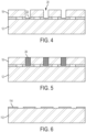
- FIGS. 1-5 there is shown a process in accordance with one or more embodiments of forming a bottom-up superconducting TSV.
- a base substrate 12 e.g., a silicon wafer.
- a thin layer of a superconducting metal 14 is blanket deposited at a thickness of about 10 nanometers (nm) to about 5 microns ( ⁇ m) onto the base substrate 12.
- the superconducting metal is deposited at a thickness of about 10 nm to about 1000 nm, and in still other embodiments, the superconducting metal is deposited at a thickness of about 20 nm to about 500 nm.
- the superconducting metal can be aluminum, gallium, indium, lanthanum, molybdenum, niobium, rhenium, ruthenium, tin, tantalum, titanium, zinc, zirconium, alloys thereof, and the like.
- the superconducting metal generally in addition to being superconducting, functions in a manner similar to a seed layer typically used in copper electroplating processes as will be discussed in greater detail below.
- the thin layer of superconducting metal 14 can be deposited onto the base substrate 12 without previous treatment by evaporation, sputtering or by electroplating. In some cases the substrate can be cleaned prior to deposition of superconducting metal 14, and in addition a relatively thin adhesion layer (e.g., a thickness of 2 nm to 20 nm) such as titanium or tantalum can be deposited prior to layer 14.
- the layer of superconducting metal 14 is then lithographically patterned, which can include forming a photoresist (e.g., organic, inorganic or hybrid) atop the layer of the superconducting metal 14.
- the photoresist can be formed utilizing a deposition process such as, for example, CVD, PECVD, spin-on coating or the like. Following formation of the photoresist, the photoresist is exposed to a desired pattern of radiation. Next, the exposed photoresist is developed utilizing a conventional resist development process. After the development step, a selective etching step can be performed to transfer the pattern from the patterned photoresist into at the layer of superconducting metal 14 stopping at the silicon layer.
- a deposition process such as, for example, CVD, PECVD, spin-on coating or the like.
- the etching step used in forming the patterned superconducting metal 14 can include a dry etching process (including, for example, reactive ion etching, ion beam etching, plasma etching or laser ablation), a wet chemical etching process or any combination thereof.
- FIG. 2 there is depicted a cap substrate 18.
- a layer of superconducting metal layer 16 is deposited onto a cap substrate 18.
- the superconducting metal 16 can be the same as the superconducting metal 14 formed on the base substrate 12.
- the layers of superconducting metals 14, 16 can be formed of aluminum.
- the cap substrate 18 can be of the same material as the base substrate 12, e.g., a silicon wafer.
- the superconducting metal 16 can be deposited at the same or different thickness as superconducting layer 14. Generally, superconducting metal 16 can be blanket deposited onto the cap substrate 18 at a thickness of about 10 nanometers (nm) to about 5 microns ( ⁇ m). In one or more other embodiments, the superconducting metal is deposited at a thickness of about 10 nm to about 1000 nm, and in still other embodiments, the superconducting metal is deposited at a thickness of about 20 nm to about 500 nm.
- the superconducting metals 14, 16 can be dissimilar or similar depending on the desired application.
- the layer of superconducting metal 16 is then lithographically patterned in the manner described above.
- Vias 20 are then formed in the cap substrate 18 by lithographically patterning and anisotropically etching the silicon substrate.
- the vias 20 will be utilized to define the TSVs and extend partly through the cap substrate 18.
- the vias can extend to a depth of about 10 microns ( ⁇ m) to as much as about 350 ⁇ m depending on the initial thickness into the silicon substrate, which typically have a thickness generally depending on diameter of about 275 ⁇ m to about 775 ⁇ m.
- the via depth into the cap substrate 18 is about 10 ⁇ m to about 250 ⁇ m, and in still other embodiments, the via depth into the cap substrate 18 is at about 20 ⁇ m to about 150 ⁇ m.
- the silicon substrate can be subjected to wet or dry etching to form the vias.
- the resulting pattern of the superconducting metal 16 and vias 20 in the cap substrate 18 are such that a portion of the superconducting material 16 surrounds a perimeter top surface about the via 20.
- the cap substrate 18 including the patterned superconducting metal 16 and vias 20 thereon is then inverted and bonded to the base substrate 12 such as by thermocompression bonding, also referred to as diffusion bonding.
- the surrounding portions of the superconducting metal 16 in the cap substrate are mated to the corresponding patterned superconducting metal 14 on the base substrate 12. That is, the portion of the superconducting material 16 surrounding the perimeter top surface of the vias 20 contacts the corresponding patterned superconducting metal 14 on the base substrate 12.
- the superconducting metals 14, 16 on each substrate 12, 18 can be brought together into atomic contact by applying force and heat simultaneously to bond the cap substrate 18 to the base substrate 12 as shown.
- the resulting structure includes the surrounding portion of superconducting metal 16 about the perimeter from the cap substrate 18 is bonded to a corresponding portion of the superconducting metal 14 in the base substrate 12 whereas the inverted vias 20 include a superconducting metal layer (from the base substrate 12) at the bottom 22 of each via 20.
- thermocompression bonding aluminum on one substrate can be bonded to aluminum on another substrate by subjecting the substrates to a bonding temperature from about 400 °C to about 450 °C with an applied force above 70 kN for 20 to 45 min, although higher or lower temperatures and forces can be used for different superconducting metals.
- the cap substrate 18 is subjected to a wafer backgrinding process to remove a portion of the cap substrate so as to expose and open the vias 20.
- the backgrinding process generally includes application of a slurry of coarse particles to coarsely grind the wafer and remove a bulk of the wafer thickness. A finer grit is then used to polish the wafer. The coarse grinding can be used to remove about 90 percent of the substrate.
- the superconducting metal surface 22 at the bottom of the vias 20 is cleaned to remove any oxide thereon. Cleaning can include applying an etchant configured to selectively remove the oxide and any residual slurry contaminants from the backgrinding process.
- the superconducting metal surface at the via bottom 22 can be prepped for filling by an optional electroless plating.
- a superconducting metal such as zinc or tin can be electrolessly plated onto an aluminum layer, which can promote adhesion of the fill material during a subsequent electroplating process.
- Aluminum, by itself, is a very difficult substrate to directly plate thereon.
- the vias 20 are filled with a superconducting metal or metal alloy to form the TSV 24 by subjecting the substrate to an electroplating process by making electrical contact to the backside of the base substrate 14 and immersing the substrate into an electrolyte bath.
- the superconducting metal or metal alloy grows from the bottom up until the TSV is fully filled with the superconducting metal and ready for further processing.
- the previously deposited superconducting metals of layers 14, 16 function as a bottom electrode during the electroplating process
- the electrolyte bath can be made up of electrolyte solvent and one or more salts including a source of metal or metals to be electroplated. Often salts can also be present to improve conductivity and efficiency of the process.
- the solvent can be aprotic or at least very weakly acidic.
- the solvent should be such as to dissolve reasonable amounts of metal salts (sources of the metal being plated) and other salts to increase electrolyte conductivity.
- the solvent should be stable not only to the substrate material being electroplated but under the condition of electroplating the metal.
- the non-aqueous solvent is chosen from various stable organic liquids such as nitriles, carbonates, amides, ketones, alcohols, glycols, ethers, and the like.
- Typical solvents are acetonitrile, benzonitrile, diglyme (diethylene glycol dimethyl ether), triglyme (triethylene glycol dimethyl ether), tetraglyme (tetraethylene glycol dimethyl ether), ethylene glycol, dimethyl formamide, acetamide, acetone, methyl isobutyl ketone, tetrahydrofuran, dimethylsulfoxide, propylene and ethylene carbonates.
- the solvent can be acetonitrile, propylene carbonate or methanol. Mixtures of the above solvents can be used as well as other substances that are stable, suitable for use in an electroplating process and not reactive to the material being electroplated. More acidic solvents can be used (even water) provided that the potential required to plate the metal protects the material being electroplated from reaction with water.
- the superconducting metals can be tin, lead, zinc, cadmium, indium, alloys thereof, and combinations of these metals.
- metals such as indium, tin, lead and tin-lead alloys are utilized because of ease of plating, availability, high electrical and thermal conductivity.
- the word metal should be understood to include various superconducting alloys (e.g., tin-lead alloy) and mixtures of metals as well as pure elemental metal.
- the metals are introduced into the electroplating bath usually in the form of a salt, preferably a salt soluble in the electrolyte solvent and with an anion which is stable under conditions of the electroplating process.
- Typical anions are nitrate, perchlorate, halide (especially chloride, bromide and iodide), tetrafluoroborate, hexafluoroarsenate.
- perchlorates and nitrates are used because of availability and solubility in nonaqueous solvents.
- concentrations vary from about 0.001 Molar to saturation. Too low a concentration requires too much time to electroplate and too much replenishment during processing. Typically, concentrations are adjusted to maximize conductivity when combined with certain ionic (conducting) salts.
- the bath is typically made up of non-aqueous solvent described above, an electrochemically stable metal salt of the metal being plated (e.g., nitrate, perchlorate) and optionally a stable salt to increase ionic conductivity.
- an electrochemically stable metal salt of the metal being plated e.g., nitrate, perchlorate
- a stable salt to increase ionic conductivity e.g., nitrate, perchlorate
- concentrations are usually close to saturation, for example from about 1/10 the concentration of a saturated solution to the concentration of a saturated solution.
- concentrations from 0.1 of saturated solutions to the concentration of the saturated solution can be used.
- the bath can contain conducting salts to increase the conductivity of the bath.
- These conducting salts are typically alkali-metal salts with stable anions with good solubility in the non-aqueous solvents.
- Typical anions are the same as for the metal salts given above (nitrate, perchlorate, halides, tetrafluoroborate (e.g. sodium tetrafluoroborate) and hexafluoroaresenate (e.g., lithium hexafluroarsenate).
- tetra alkylammonium salts such as tetrabutylammonium halides and tetraethyl ammonium halides.
- Concentrations of the conducting salts can vary from 0.001 molar to saturation and are usually determined so as to maximize conductivity of the bath. Generally, concentrations near saturation (within 0.1 of saturation to saturation) are preferred.
- the electroplating process is carried out in a conventional manner with a conventional anode and the material to be plated made the cathode of an electroplating apparatus.
- a base substrate 112 is provided, e.g., a silicon wafer.
- a thin layer of a superconducting metal 114 is blanket deposited at a thickness of about 10 nanometers (nm) to about 5 microns ( ⁇ m).
- the superconducting metal is deposited at a thickness of about 10 nm to about 1000 nm, and in still other embodiments, the superconducting metal is deposited at a thickness of about 20 nm to about 500 nm.
- the superconducting metal can be a metal as previously described.
- the layer of superconducting metal 114 is then lithographically patterned to form a patterned superconducting metal as shown.
- a cap substrate 118 is provided and thin layer of a superconducting metal 120 is blanket deposited at a thickness of about 10 nanometers (nm) to about 5 microns ( ⁇ m).
- the superconducting metal is deposited at a thickness of about 10 nm to about 1000 nm, and in still other embodiments, the superconducting metal is deposited at a thickness of about 20 nm to about 500 nm.
- the superconducting metal can be a metal as previously described.
- the layer of superconducting metal 120 is then lithographically patterned to form a patterned superconducting metal similar to that provided in FIG. 6 .
- the cap substrate 118 is inverted and the patterned superconductor layer 120 is aligned with the corresponding patterned superconducting metal 114 on the base substrate 112 and subjected to thermocompression bonding to bond the cap substrate 118 to the base substrate 112.
- the cap substrate 118 is subjected to backgrinding process as described above to remove a portion of the cap substrate. The remaining thickness of the cap substrate 118 will be used to define the length of the TSV.
- the cap substrate 118 is then lithographically patterned and etched to form vias 122 therein, which are configured to land on the thermocompression bonded and patterned superconducting metals 114/120.
- the topmost exposed superconducting metal 120 is then cleaned and prepped if needed by electrolessly prepped as previously described using a superconductor such as zinc or tin to promote adhesion during the fill process
- Deposition is any process that grows, coats, or otherwise transfers a material onto the wafer.
- Available technologies include physical vapor deposition (PVD), chemical vapor deposition (CVD), electrochemical deposition (ECD), molecular beam epitaxy (MBE) and more recently, atomic layer deposition (ALD) among others.
- Removal/etching is any process that removes material from the wafer. Examples include etch processes (either wet or dry), and chemical-mechanical planarization (CMP), and the like.
- Semiconductor doping is the modification of electrical properties by doping, for example, transistor sources and drains, generally by diffusion and/or by ion implantation. These doping processes are followed by furnace annealing or by rapid thermal annealing (RTA). Annealing serves to activate the implanted dopants. Films of both conductors (e.g., poly-silicon, aluminum, copper, etc.) and insulators (e.g., various forms of silicon dioxide, silicon nitride, etc.) are used to connect and isolate transistors and their components. Selective doping of various regions of the semiconductor substrate allows the conductivity of the substrate to be changed with the application of voltage.
- RTA rapid thermal annealing
- Semiconductor lithography is the formation of three-dimensional relief images or patterns on the semiconductor substrate for subsequent transfer of the pattern to the substrate.
- the patterns are formed by a light sensitive polymer called a photo-resist.
- lithography and etch pattern transfer steps are repeated multiple times. Each pattern being printed on the wafer is aligned to the previously formed patterns and slowly the conductors, insulators and selectively doped regions are built up to form the final device.
Landscapes
- Internal Circuitry In Semiconductor Integrated Circuit Devices (AREA)
- Engineering & Computer Science (AREA)
- Manufacturing & Machinery (AREA)
- Chemical & Material Sciences (AREA)
- Chemical Kinetics & Catalysis (AREA)
- General Chemical & Material Sciences (AREA)
- Superconductor Devices And Manufacturing Methods Thereof (AREA)
Applications Claiming Priority (2)
| Application Number | Priority Date | Filing Date | Title |
|---|---|---|---|
| US15/609,860 US10157842B1 (en) | 2017-05-31 | 2017-05-31 | Semiconductor device including superconducting metal through-silicon-vias and method of manufacturing the same |
| PCT/EP2017/081792 WO2018219484A1 (en) | 2017-05-31 | 2017-12-07 | Superconducting metal through-silicon-vias |
Publications (2)
| Publication Number | Publication Date |
|---|---|
| EP3639295A1 EP3639295A1 (en) | 2020-04-22 |
| EP3639295B1 true EP3639295B1 (en) | 2023-09-13 |
Family
ID=60627639
Family Applications (1)
| Application Number | Title | Priority Date | Filing Date |
|---|---|---|---|
| EP17811292.6A Active EP3639295B1 (en) | 2017-05-31 | 2017-12-07 | Superconducting through-silicon-vias and their method of fabrication |
Country Status (6)
| Country | Link |
|---|---|
| US (3) | US10157842B1 (https=) |
| EP (1) | EP3639295B1 (https=) |
| JP (1) | JP7182834B2 (https=) |
| CN (1) | CN110622297B (https=) |
| ES (1) | ES2960054T3 (https=) |
| WO (1) | WO2018219484A1 (https=) |
Families Citing this family (12)
| Publication number | Priority date | Publication date | Assignee | Title |
|---|---|---|---|---|
| US10068181B1 (en) | 2015-04-27 | 2018-09-04 | Rigetti & Co, Inc. | Microwave integrated quantum circuits with cap wafer and methods for making the same |
| US11121301B1 (en) * | 2017-06-19 | 2021-09-14 | Rigetti & Co, Inc. | Microwave integrated quantum circuits with cap wafers and their methods of manufacture |
| US10741742B2 (en) | 2018-02-28 | 2020-08-11 | The Regents Of The University Of Colorado, A Body Corporate | Enhanced superconducting transition temperature in electroplated rhenium |
| US11158781B2 (en) | 2019-11-27 | 2021-10-26 | International Business Machines Corporation | Permanent wafer handlers with through silicon vias for thermalization and qubit modification |
| US20210280765A1 (en) * | 2020-03-06 | 2021-09-09 | The Board Of Trustees Of The University Of Alabama | Superconducting carrier and cables for quantum device chips and method of fabrication |
| CN112420604B (zh) * | 2020-11-20 | 2022-12-06 | 中国科学院半导体研究所 | 一种基于热压键合的tsv垂直电学互连器件的制备方法 |
| US12033981B2 (en) | 2020-12-16 | 2024-07-09 | International Business Machines Corporation | Create a protected layer for interconnects and devices in a packaged quantum structure |
| FI20215520A1 (en) * | 2021-05-04 | 2022-11-05 | Iqm Finland Oy | Superconducting vias in the substrate |
| JP2024526085A (ja) | 2021-06-11 | 2024-07-17 | シーク, インコーポレイテッド | 超伝導量子回路のための磁束バイアスのシステム及び方法 |
| CN115000286A (zh) * | 2022-07-13 | 2022-09-02 | 材料科学姑苏实验室 | 一种晶圆孔道填充方法、填充装置、转接片和用途 |
| CN117460398B (zh) * | 2023-10-30 | 2026-01-13 | 本源量子计算科技(合肥)股份有限公司 | 超导线路及其制造方法 |
| JP2026028554A (ja) | 2024-08-07 | 2026-02-20 | 富士通株式会社 | デバイスの製造方法及びデバイス |
Citations (2)
| Publication number | Priority date | Publication date | Assignee | Title |
|---|---|---|---|---|
| US20100240174A1 (en) * | 2007-10-05 | 2010-09-23 | Jin Yu | Via Using Zn or Zn Alloys and Its Making Method, 3D Chip Stack Packages Using Thereof |
| US20140274725A1 (en) * | 2013-03-15 | 2014-09-18 | International Business Machines Corporation | Chip mode isolation and cross-talk reduction through buried metal layers and through-vias |
Family Cites Families (19)
| Publication number | Priority date | Publication date | Assignee | Title |
|---|---|---|---|---|
| CA1329952C (en) * | 1987-04-27 | 1994-05-31 | Yoshihiko Imanaka | Multi-layer superconducting circuit substrate and process for manufacturing same |
| EP0358879A3 (en) * | 1988-09-13 | 1991-02-27 | Hewlett-Packard Company | Method of making high density interconnects |
| EP0612114B1 (en) * | 1993-02-15 | 1997-05-14 | Sumitomo Electric Industries, Ltd. | Method for forming a patterned oxide superconductor thin film |
| US6100194A (en) | 1998-06-22 | 2000-08-08 | Stmicroelectronics, Inc. | Silver metallization by damascene method |
| US6228675B1 (en) | 1999-07-23 | 2001-05-08 | Agilent Technologies, Inc. | Microcap wafer-level package with vias |
| SG111972A1 (en) * | 2002-10-17 | 2005-06-29 | Agency Science Tech & Res | Wafer-level package for micro-electro-mechanical systems |
| US8084695B2 (en) | 2007-01-10 | 2011-12-27 | Hsu Hsiuan-Ju | Via structure for improving signal integrity |
| US7696064B2 (en) * | 2007-10-11 | 2010-04-13 | Skyworks Solutions, Inc. | Methods for forming a through via |
| US7776741B2 (en) | 2008-08-18 | 2010-08-17 | Novellus Systems, Inc. | Process for through silicon via filing |
| JP5471268B2 (ja) * | 2008-12-26 | 2014-04-16 | 大日本印刷株式会社 | 貫通電極基板及びその製造方法 |
| EP3098865B1 (en) | 2009-02-27 | 2018-10-03 | D-Wave Systems Inc. | Method for fabricating a superconducting integrated circuit |
| JP2011026680A (ja) | 2009-07-28 | 2011-02-10 | Renesas Electronics Corp | 半導体装置の製造方法及び半導体装置の製造装置 |
| CN102024782B (zh) | 2010-10-12 | 2012-07-25 | 北京大学 | 三维垂直互联结构及其制作方法 |
| US9768371B2 (en) * | 2012-03-08 | 2017-09-19 | D-Wave Systems Inc. | Systems and methods for fabrication of superconducting integrated circuits |
| CN102602881B (zh) * | 2012-04-01 | 2014-04-09 | 杭州士兰集成电路有限公司 | Mems封帽硅片的多硅槽形成方法及其刻蚀掩膜结构 |
| KR20140081191A (ko) * | 2012-12-21 | 2014-07-01 | 삼성전기주식회사 | 방열기판 및 그 제조 방법 |
| US9396992B2 (en) * | 2014-03-04 | 2016-07-19 | Taiwan Semiconductor Manufacturing Co., Ltd. | Method of using a barrier-seed tool for forming fine-pitched metal interconnects |
| KR20160046169A (ko) * | 2014-10-20 | 2016-04-28 | 삼성디스플레이 주식회사 | 광학 마스크 |
| US9761561B2 (en) * | 2015-03-18 | 2017-09-12 | Globalfoundries Singapore Pte. Ltd. | Edge structure for backgrinding asymmetrical bonded wafer |
-
2017
- 2017-05-31 US US15/609,860 patent/US10157842B1/en active Active
- 2017-12-07 JP JP2019564442A patent/JP7182834B2/ja active Active
- 2017-12-07 CN CN201780090283.5A patent/CN110622297B/zh active Active
- 2017-12-07 WO PCT/EP2017/081792 patent/WO2018219484A1/en not_active Ceased
- 2017-12-07 ES ES17811292T patent/ES2960054T3/es active Active
- 2017-12-07 EP EP17811292.6A patent/EP3639295B1/en active Active
-
2018
- 2018-06-06 US US16/001,302 patent/US10504842B1/en active Active
- 2018-12-11 US US16/215,913 patent/US10833016B2/en active Active
Patent Citations (2)
| Publication number | Priority date | Publication date | Assignee | Title |
|---|---|---|---|---|
| US20100240174A1 (en) * | 2007-10-05 | 2010-09-23 | Jin Yu | Via Using Zn or Zn Alloys and Its Making Method, 3D Chip Stack Packages Using Thereof |
| US20140274725A1 (en) * | 2013-03-15 | 2014-09-18 | International Business Machines Corporation | Chip mode isolation and cross-talk reduction through buried metal layers and through-vias |
Also Published As
| Publication number | Publication date |
|---|---|
| JP7182834B2 (ja) | 2022-12-05 |
| US10833016B2 (en) | 2020-11-10 |
| CN110622297A (zh) | 2019-12-27 |
| JP2020522128A (ja) | 2020-07-27 |
| US20200251419A1 (en) | 2020-08-06 |
| US20180350749A1 (en) | 2018-12-06 |
| US10157842B1 (en) | 2018-12-18 |
| EP3639295A1 (en) | 2020-04-22 |
| WO2018219484A1 (en) | 2018-12-06 |
| US10504842B1 (en) | 2019-12-10 |
| ES2960054T3 (es) | 2024-02-29 |
| CN110622297B (zh) | 2023-09-01 |
Similar Documents
| Publication | Publication Date | Title |
|---|---|---|
| EP3639295B1 (en) | Superconducting through-silicon-vias and their method of fabrication | |
| US10686126B2 (en) | Back end of line metallization structures | |
| JP5801889B2 (ja) | 裏面コンタクトがビアファースト構造体又はビアミドル構造体で接続された超小型電子素子 | |
| TWI495071B (zh) | 具有穿透基板互連之半導體 | |
| US10396013B2 (en) | Advanced through substrate via metallization in three dimensional semiconductor integration | |
| US10971398B2 (en) | Cobalt interconnect structure including noble metal layer | |
| US10903161B2 (en) | Back end of line metallization structure | |
| US10312181B2 (en) | Advanced through substrate via metallization in three dimensional semiconductor integration | |
| US11031339B2 (en) | Metal interconnects | |
| US20250266378A1 (en) | Connector and method for forming the same | |
| EP3622555B1 (en) | Through-substrate-vias with self-aligned solder bumps | |
| US20240030222A1 (en) | Trapping layer for a radio frequency die and methods of formation | |
| US10916503B2 (en) | Back end of line metallization structure | |
| WO2018063405A1 (en) | Microelectronic devices and methods for enhancing interconnect reliability performance using an in-situ nickel barrier layer |
Legal Events
| Date | Code | Title | Description |
|---|---|---|---|
| STAA | Information on the status of an ep patent application or granted ep patent |
Free format text: STATUS: UNKNOWN |
|
| STAA | Information on the status of an ep patent application or granted ep patent |
Free format text: STATUS: THE INTERNATIONAL PUBLICATION HAS BEEN MADE |
|
| PUAI | Public reference made under article 153(3) epc to a published international application that has entered the european phase |
Free format text: ORIGINAL CODE: 0009012 |
|
| STAA | Information on the status of an ep patent application or granted ep patent |
Free format text: STATUS: REQUEST FOR EXAMINATION WAS MADE |
|
| 17P | Request for examination filed |
Effective date: 20191202 |
|
| AK | Designated contracting states |
Kind code of ref document: A1 Designated state(s): AL AT BE BG CH CY CZ DE DK EE ES FI FR GB GR HR HU IE IS IT LI LT LU LV MC MK MT NL NO PL PT RO RS SE SI SK SM TR |
|
| AX | Request for extension of the european patent |
Extension state: BA ME |
|
| DAV | Request for validation of the european patent (deleted) | ||
| DAX | Request for extension of the european patent (deleted) | ||
| STAA | Information on the status of an ep patent application or granted ep patent |
Free format text: STATUS: EXAMINATION IS IN PROGRESS |
|
| 17Q | First examination report despatched |
Effective date: 20211021 |
|
| RIC1 | Information provided on ipc code assigned before grant |
Ipc: H01L 21/288 20060101ALN20230317BHEP Ipc: H01L 23/532 20060101ALI20230317BHEP Ipc: H01L 23/48 20060101ALI20230317BHEP Ipc: H01L 21/768 20060101AFI20230317BHEP |
|
| GRAP | Despatch of communication of intention to grant a patent |
Free format text: ORIGINAL CODE: EPIDOSNIGR1 |
|
| STAA | Information on the status of an ep patent application or granted ep patent |
Free format text: STATUS: GRANT OF PATENT IS INTENDED |
|
| INTG | Intention to grant announced |
Effective date: 20230515 |
|
| RAP3 | Party data changed (applicant data changed or rights of an application transferred) |
Owner name: INTERNATIONAL BUSINESS MACHINES CORPORATION |
|
| GRAS | Grant fee paid |
Free format text: ORIGINAL CODE: EPIDOSNIGR3 |
|
| GRAA | (expected) grant |
Free format text: ORIGINAL CODE: 0009210 |
|
| STAA | Information on the status of an ep patent application or granted ep patent |
Free format text: STATUS: THE PATENT HAS BEEN GRANTED |
|
| AK | Designated contracting states |
Kind code of ref document: B1 Designated state(s): AL AT BE BG CH CY CZ DE DK EE ES FI FR GB GR HR HU IE IS IT LI LT LU LV MC MK MT NL NO PL PT RO RS SE SI SK SM TR |
|
| REG | Reference to a national code |
Ref country code: GB Ref legal event code: FG4D |
|
| REG | Reference to a national code |
Ref country code: CH Ref legal event code: EP |
|
| REG | Reference to a national code |
Ref country code: DE Ref legal event code: R096 Ref document number: 602017074225 Country of ref document: DE |
|
| REG | Reference to a national code |
Ref country code: IE Ref legal event code: FG4D |
|
| REG | Reference to a national code |
Ref country code: NL Ref legal event code: FP |
|
| P01 | Opt-out of the competence of the unified patent court (upc) registered |
Effective date: 20230929 |
|
| REG | Reference to a national code |
Ref country code: LT Ref legal event code: MG9D |
|
| PG25 | Lapsed in a contracting state [announced via postgrant information from national office to epo] |
Ref country code: GR Free format text: LAPSE BECAUSE OF FAILURE TO SUBMIT A TRANSLATION OF THE DESCRIPTION OR TO PAY THE FEE WITHIN THE PRESCRIBED TIME-LIMIT Effective date: 20231214 |
|
| PG25 | Lapsed in a contracting state [announced via postgrant information from national office to epo] |
Ref country code: SE Free format text: LAPSE BECAUSE OF FAILURE TO SUBMIT A TRANSLATION OF THE DESCRIPTION OR TO PAY THE FEE WITHIN THE PRESCRIBED TIME-LIMIT Effective date: 20230913 Ref country code: RS Free format text: LAPSE BECAUSE OF FAILURE TO SUBMIT A TRANSLATION OF THE DESCRIPTION OR TO PAY THE FEE WITHIN THE PRESCRIBED TIME-LIMIT Effective date: 20230913 Ref country code: NO Free format text: LAPSE BECAUSE OF FAILURE TO SUBMIT A TRANSLATION OF THE DESCRIPTION OR TO PAY THE FEE WITHIN THE PRESCRIBED TIME-LIMIT Effective date: 20231213 Ref country code: LV Free format text: LAPSE BECAUSE OF FAILURE TO SUBMIT A TRANSLATION OF THE DESCRIPTION OR TO PAY THE FEE WITHIN THE PRESCRIBED TIME-LIMIT Effective date: 20230913 Ref country code: LT Free format text: LAPSE BECAUSE OF FAILURE TO SUBMIT A TRANSLATION OF THE DESCRIPTION OR TO PAY THE FEE WITHIN THE PRESCRIBED TIME-LIMIT Effective date: 20230913 Ref country code: HR Free format text: LAPSE BECAUSE OF FAILURE TO SUBMIT A TRANSLATION OF THE DESCRIPTION OR TO PAY THE FEE WITHIN THE PRESCRIBED TIME-LIMIT Effective date: 20230913 Ref country code: GR Free format text: LAPSE BECAUSE OF FAILURE TO SUBMIT A TRANSLATION OF THE DESCRIPTION OR TO PAY THE FEE WITHIN THE PRESCRIBED TIME-LIMIT Effective date: 20231214 Ref country code: FI Free format text: LAPSE BECAUSE OF FAILURE TO SUBMIT A TRANSLATION OF THE DESCRIPTION OR TO PAY THE FEE WITHIN THE PRESCRIBED TIME-LIMIT Effective date: 20230913 |
|
| REG | Reference to a national code |
Ref country code: AT Ref legal event code: MK05 Ref document number: 1612187 Country of ref document: AT Kind code of ref document: T Effective date: 20230913 |
|
| REG | Reference to a national code |
Ref country code: ES Ref legal event code: FG2A Ref document number: 2960054 Country of ref document: ES Kind code of ref document: T3 Effective date: 20240229 |
|
| PG25 | Lapsed in a contracting state [announced via postgrant information from national office to epo] |
Ref country code: IS Free format text: LAPSE BECAUSE OF FAILURE TO SUBMIT A TRANSLATION OF THE DESCRIPTION OR TO PAY THE FEE WITHIN THE PRESCRIBED TIME-LIMIT Effective date: 20240113 |
|
| PG25 | Lapsed in a contracting state [announced via postgrant information from national office to epo] |
Ref country code: AT Free format text: LAPSE BECAUSE OF FAILURE TO SUBMIT A TRANSLATION OF THE DESCRIPTION OR TO PAY THE FEE WITHIN THE PRESCRIBED TIME-LIMIT Effective date: 20230913 |
|
| PG25 | Lapsed in a contracting state [announced via postgrant information from national office to epo] |
Ref country code: SM Free format text: LAPSE BECAUSE OF FAILURE TO SUBMIT A TRANSLATION OF THE DESCRIPTION OR TO PAY THE FEE WITHIN THE PRESCRIBED TIME-LIMIT Effective date: 20230913 Ref country code: RO Free format text: LAPSE BECAUSE OF FAILURE TO SUBMIT A TRANSLATION OF THE DESCRIPTION OR TO PAY THE FEE WITHIN THE PRESCRIBED TIME-LIMIT Effective date: 20230913 Ref country code: IS Free format text: LAPSE BECAUSE OF FAILURE TO SUBMIT A TRANSLATION OF THE DESCRIPTION OR TO PAY THE FEE WITHIN THE PRESCRIBED TIME-LIMIT Effective date: 20240113 Ref country code: EE Free format text: LAPSE BECAUSE OF FAILURE TO SUBMIT A TRANSLATION OF THE DESCRIPTION OR TO PAY THE FEE WITHIN THE PRESCRIBED TIME-LIMIT Effective date: 20230913 Ref country code: CZ Free format text: LAPSE BECAUSE OF FAILURE TO SUBMIT A TRANSLATION OF THE DESCRIPTION OR TO PAY THE FEE WITHIN THE PRESCRIBED TIME-LIMIT Effective date: 20230913 Ref country code: AT Free format text: LAPSE BECAUSE OF FAILURE TO SUBMIT A TRANSLATION OF THE DESCRIPTION OR TO PAY THE FEE WITHIN THE PRESCRIBED TIME-LIMIT Effective date: 20230913 Ref country code: PT Free format text: LAPSE BECAUSE OF FAILURE TO SUBMIT A TRANSLATION OF THE DESCRIPTION OR TO PAY THE FEE WITHIN THE PRESCRIBED TIME-LIMIT Effective date: 20240115 Ref country code: SK Free format text: LAPSE BECAUSE OF FAILURE TO SUBMIT A TRANSLATION OF THE DESCRIPTION OR TO PAY THE FEE WITHIN THE PRESCRIBED TIME-LIMIT Effective date: 20230913 |
|
| PG25 | Lapsed in a contracting state [announced via postgrant information from national office to epo] |
Ref country code: PL Free format text: LAPSE BECAUSE OF FAILURE TO SUBMIT A TRANSLATION OF THE DESCRIPTION OR TO PAY THE FEE WITHIN THE PRESCRIBED TIME-LIMIT Effective date: 20230913 Ref country code: IT Free format text: LAPSE BECAUSE OF FAILURE TO SUBMIT A TRANSLATION OF THE DESCRIPTION OR TO PAY THE FEE WITHIN THE PRESCRIBED TIME-LIMIT Effective date: 20230913 |
|
| REG | Reference to a national code |
Ref country code: DE Ref legal event code: R097 Ref document number: 602017074225 Country of ref document: DE |
|
| PG25 | Lapsed in a contracting state [announced via postgrant information from national office to epo] |
Ref country code: DK Free format text: LAPSE BECAUSE OF FAILURE TO SUBMIT A TRANSLATION OF THE DESCRIPTION OR TO PAY THE FEE WITHIN THE PRESCRIBED TIME-LIMIT Effective date: 20230913 |
|
| PLBE | No opposition filed within time limit |
Free format text: ORIGINAL CODE: 0009261 |
|
| STAA | Information on the status of an ep patent application or granted ep patent |
Free format text: STATUS: NO OPPOSITION FILED WITHIN TIME LIMIT |
|
| PG25 | Lapsed in a contracting state [announced via postgrant information from national office to epo] |
Ref country code: DK Free format text: LAPSE BECAUSE OF FAILURE TO SUBMIT A TRANSLATION OF THE DESCRIPTION OR TO PAY THE FEE WITHIN THE PRESCRIBED TIME-LIMIT Effective date: 20230913 |
|
| REG | Reference to a national code |
Ref country code: CH Ref legal event code: PL |
|
| 26N | No opposition filed |
Effective date: 20240614 |
|
| PG25 | Lapsed in a contracting state [announced via postgrant information from national office to epo] |
Ref country code: LU Free format text: LAPSE BECAUSE OF NON-PAYMENT OF DUE FEES Effective date: 20231207 |
|
| PG25 | Lapsed in a contracting state [announced via postgrant information from national office to epo] |
Ref country code: MC Free format text: LAPSE BECAUSE OF FAILURE TO SUBMIT A TRANSLATION OF THE DESCRIPTION OR TO PAY THE FEE WITHIN THE PRESCRIBED TIME-LIMIT Effective date: 20230913 |
|
| REG | Reference to a national code |
Ref country code: BE Ref legal event code: MM Effective date: 20231231 |
|
| PG25 | Lapsed in a contracting state [announced via postgrant information from national office to epo] |
Ref country code: MC Free format text: LAPSE BECAUSE OF FAILURE TO SUBMIT A TRANSLATION OF THE DESCRIPTION OR TO PAY THE FEE WITHIN THE PRESCRIBED TIME-LIMIT Effective date: 20230913 Ref country code: LU Free format text: LAPSE BECAUSE OF NON-PAYMENT OF DUE FEES Effective date: 20231207 |
|
| PG25 | Lapsed in a contracting state [announced via postgrant information from national office to epo] |
Ref country code: BE Free format text: LAPSE BECAUSE OF NON-PAYMENT OF DUE FEES Effective date: 20231231 |
|
| PG25 | Lapsed in a contracting state [announced via postgrant information from national office to epo] |
Ref country code: CH Free format text: LAPSE BECAUSE OF NON-PAYMENT OF DUE FEES Effective date: 20231231 |
|
| PG25 | Lapsed in a contracting state [announced via postgrant information from national office to epo] |
Ref country code: SI Free format text: LAPSE BECAUSE OF FAILURE TO SUBMIT A TRANSLATION OF THE DESCRIPTION OR TO PAY THE FEE WITHIN THE PRESCRIBED TIME-LIMIT Effective date: 20230913 |
|
| PG25 | Lapsed in a contracting state [announced via postgrant information from national office to epo] |
Ref country code: SI Free format text: LAPSE BECAUSE OF FAILURE TO SUBMIT A TRANSLATION OF THE DESCRIPTION OR TO PAY THE FEE WITHIN THE PRESCRIBED TIME-LIMIT Effective date: 20230913 Ref country code: CH Free format text: LAPSE BECAUSE OF NON-PAYMENT OF DUE FEES Effective date: 20231231 Ref country code: BE Free format text: LAPSE BECAUSE OF NON-PAYMENT OF DUE FEES Effective date: 20231231 |
|
| PG25 | Lapsed in a contracting state [announced via postgrant information from national office to epo] |
Ref country code: BG Free format text: LAPSE BECAUSE OF FAILURE TO SUBMIT A TRANSLATION OF THE DESCRIPTION OR TO PAY THE FEE WITHIN THE PRESCRIBED TIME-LIMIT Effective date: 20230913 |
|
| PG25 | Lapsed in a contracting state [announced via postgrant information from national office to epo] |
Ref country code: BG Free format text: LAPSE BECAUSE OF FAILURE TO SUBMIT A TRANSLATION OF THE DESCRIPTION OR TO PAY THE FEE WITHIN THE PRESCRIBED TIME-LIMIT Effective date: 20230913 |
|
| PG25 | Lapsed in a contracting state [announced via postgrant information from national office to epo] |
Ref country code: CY Free format text: LAPSE BECAUSE OF FAILURE TO SUBMIT A TRANSLATION OF THE DESCRIPTION OR TO PAY THE FEE WITHIN THE PRESCRIBED TIME-LIMIT; INVALID AB INITIO Effective date: 20171207 |
|
| PG25 | Lapsed in a contracting state [announced via postgrant information from national office to epo] |
Ref country code: HU Free format text: LAPSE BECAUSE OF FAILURE TO SUBMIT A TRANSLATION OF THE DESCRIPTION OR TO PAY THE FEE WITHIN THE PRESCRIBED TIME-LIMIT; INVALID AB INITIO Effective date: 20171207 |
|
| REG | Reference to a national code |
Ref country code: DE Ref legal event code: R079 Ref document number: 602017074225 Country of ref document: DE Free format text: PREVIOUS MAIN CLASS: H01L0021768000 Ipc: H10W0020000000 |
|
| PG25 | Lapsed in a contracting state [announced via postgrant information from national office to epo] |
Ref country code: TR Free format text: LAPSE BECAUSE OF FAILURE TO SUBMIT A TRANSLATION OF THE DESCRIPTION OR TO PAY THE FEE WITHIN THE PRESCRIBED TIME-LIMIT Effective date: 20230913 |
|
| PGFP | Annual fee paid to national office [announced via postgrant information from national office to epo] |
Ref country code: DE Payment date: 20251110 Year of fee payment: 9 |
|
| PGFP | Annual fee paid to national office [announced via postgrant information from national office to epo] |
Ref country code: GB Payment date: 20251201 Year of fee payment: 9 |
|
| PGFP | Annual fee paid to national office [announced via postgrant information from national office to epo] |
Ref country code: FR Payment date: 20251230 Year of fee payment: 9 Ref country code: NL Payment date: 20251222 Year of fee payment: 9 |
|
| PGFP | Annual fee paid to national office [announced via postgrant information from national office to epo] |
Ref country code: IE Payment date: 20251218 Year of fee payment: 9 |
|
| PGFP | Annual fee paid to national office [announced via postgrant information from national office to epo] |
Ref country code: ES Payment date: 20260122 Year of fee payment: 9 |