EP3637571B1 - Schaltung mit warnung vor kritischen betriebszuständen, entsprechende vorrichtung und verfahren - Google Patents
Schaltung mit warnung vor kritischen betriebszuständen, entsprechende vorrichtung und verfahren Download PDFInfo
- Publication number
- EP3637571B1 EP3637571B1 EP19198276.8A EP19198276A EP3637571B1 EP 3637571 B1 EP3637571 B1 EP 3637571B1 EP 19198276 A EP19198276 A EP 19198276A EP 3637571 B1 EP3637571 B1 EP 3637571B1
- Authority
- EP
- European Patent Office
- Prior art keywords
- voltage
- signal
- circuit
- burst
- warning
- Prior art date
- Legal status (The legal status is an assumption and is not a legal conclusion. Google has not performed a legal analysis and makes no representation as to the accuracy of the status listed.)
- Active
Links
Images
Classifications
-
- H—ELECTRICITY
- H02—GENERATION; CONVERSION OR DISTRIBUTION OF ELECTRIC POWER
- H02H—EMERGENCY PROTECTIVE CIRCUIT ARRANGEMENTS
- H02H1/00—Details of emergency protective circuit arrangements
- H02H1/0007—Details of emergency protective circuit arrangements concerning the detecting means
-
- G—PHYSICS
- G06—COMPUTING OR CALCULATING; COUNTING
- G06F—ELECTRIC DIGITAL DATA PROCESSING
- G06F1/00—Details not covered by groups G06F3/00 - G06F13/00 and G06F21/00
- G06F1/16—Constructional details or arrangements
- G06F1/20—Cooling means
- G06F1/206—Cooling means comprising thermal management
-
- H—ELECTRICITY
- H02—GENERATION; CONVERSION OR DISTRIBUTION OF ELECTRIC POWER
- H02H—EMERGENCY PROTECTIVE CIRCUIT ARRANGEMENTS
- H02H5/00—Emergency protective circuit arrangements for automatic disconnection directly responsive to an undesired change from normal non-electric working conditions with or without subsequent reconnection
- H02H5/04—Emergency protective circuit arrangements for automatic disconnection directly responsive to an undesired change from normal non-electric working conditions with or without subsequent reconnection responsive to abnormal temperature
- H02H5/041—Emergency protective circuit arrangements for automatic disconnection directly responsive to an undesired change from normal non-electric working conditions with or without subsequent reconnection responsive to abnormal temperature additionally responsive to excess current
-
- G—PHYSICS
- G06—COMPUTING OR CALCULATING; COUNTING
- G06F—ELECTRIC DIGITAL DATA PROCESSING
- G06F1/00—Details not covered by groups G06F3/00 - G06F13/00 and G06F21/00
- G06F1/26—Power supply means, e.g. regulation thereof
-
- G—PHYSICS
- G06—COMPUTING OR CALCULATING; COUNTING
- G06F—ELECTRIC DIGITAL DATA PROCESSING
- G06F1/00—Details not covered by groups G06F3/00 - G06F13/00 and G06F21/00
- G06F1/26—Power supply means, e.g. regulation thereof
- G06F1/28—Supervision thereof, e.g. detecting power-supply failure by out of limits supervision
-
- G—PHYSICS
- G08—SIGNALLING
- G08B—SIGNALLING OR CALLING SYSTEMS; ORDER TELEGRAPHS; ALARM SYSTEMS
- G08B21/00—Alarms responsive to a single specified undesired or abnormal condition and not otherwise provided for
- G08B21/18—Status alarms
- G08B21/185—Electrical failure alarms
-
- H—ELECTRICITY
- H02—GENERATION; CONVERSION OR DISTRIBUTION OF ELECTRIC POWER
- H02H—EMERGENCY PROTECTIVE CIRCUIT ARRANGEMENTS
- H02H1/00—Details of emergency protective circuit arrangements
- H02H1/0092—Details of emergency protective circuit arrangements concerning the data processing means, e.g. expert systems, neural networks
-
- H—ELECTRICITY
- H02—GENERATION; CONVERSION OR DISTRIBUTION OF ELECTRIC POWER
- H02H—EMERGENCY PROTECTIVE CIRCUIT ARRANGEMENTS
- H02H3/00—Emergency protective circuit arrangements for automatic disconnection directly responsive to an undesired change from normal electric working condition with or without subsequent reconnection ; integrated protection
- H02H3/02—Details
- H02H3/04—Details with warning or supervision in addition to disconnection, e.g. for indicating that protective apparatus has functioned
-
- H—ELECTRICITY
- H02—GENERATION; CONVERSION OR DISTRIBUTION OF ELECTRIC POWER
- H02H—EMERGENCY PROTECTIVE CIRCUIT ARRANGEMENTS
- H02H3/00—Emergency protective circuit arrangements for automatic disconnection directly responsive to an undesired change from normal electric working condition with or without subsequent reconnection ; integrated protection
- H02H3/20—Emergency protective circuit arrangements for automatic disconnection directly responsive to an undesired change from normal electric working condition with or without subsequent reconnection ; integrated protection responsive to excess voltage
- H02H3/202—Emergency protective circuit arrangements for automatic disconnection directly responsive to an undesired change from normal electric working condition with or without subsequent reconnection ; integrated protection responsive to excess voltage for DC systems
-
- H—ELECTRICITY
- H02—GENERATION; CONVERSION OR DISTRIBUTION OF ELECTRIC POWER
- H02H—EMERGENCY PROTECTIVE CIRCUIT ARRANGEMENTS
- H02H5/00—Emergency protective circuit arrangements for automatic disconnection directly responsive to an undesired change from normal non-electric working conditions with or without subsequent reconnection
- H02H5/04—Emergency protective circuit arrangements for automatic disconnection directly responsive to an undesired change from normal non-electric working conditions with or without subsequent reconnection responsive to abnormal temperature
-
- H—ELECTRICITY
- H02—GENERATION; CONVERSION OR DISTRIBUTION OF ELECTRIC POWER
- H02H—EMERGENCY PROTECTIVE CIRCUIT ARRANGEMENTS
- H02H7/00—Emergency protective circuit arrangements specially adapted for specific types of electric machines or apparatus or for sectionalised protection of cable or line systems, and effecting automatic switching in the event of an undesired change from normal working conditions
- H02H7/10—Emergency protective circuit arrangements specially adapted for specific types of electric machines or apparatus or for sectionalised protection of cable or line systems, and effecting automatic switching in the event of an undesired change from normal working conditions for converters; for rectifiers
- H02H7/12—Emergency protective circuit arrangements specially adapted for specific types of electric machines or apparatus or for sectionalised protection of cable or line systems, and effecting automatic switching in the event of an undesired change from normal working conditions for converters; for rectifiers for static converters or rectifiers
- H02H7/1213—Emergency protective circuit arrangements specially adapted for specific types of electric machines or apparatus or for sectionalised protection of cable or line systems, and effecting automatic switching in the event of an undesired change from normal working conditions for converters; for rectifiers for static converters or rectifiers for DC-DC converters
-
- H—ELECTRICITY
- H02—GENERATION; CONVERSION OR DISTRIBUTION OF ELECTRIC POWER
- H02H—EMERGENCY PROTECTIVE CIRCUIT ARRANGEMENTS
- H02H7/00—Emergency protective circuit arrangements specially adapted for specific types of electric machines or apparatus or for sectionalised protection of cable or line systems, and effecting automatic switching in the event of an undesired change from normal working conditions
- H02H7/20—Emergency protective circuit arrangements specially adapted for specific types of electric machines or apparatus or for sectionalised protection of cable or line systems, and effecting automatic switching in the event of an undesired change from normal working conditions for electronic equipment
-
- H—ELECTRICITY
- H03—ELECTRONIC CIRCUITRY
- H03K—PULSE TECHNIQUE
- H03K19/00—Logic circuits, i.e. having at least two inputs acting on one output; Inverting circuits
- H03K19/003—Modifications for increasing the reliability for protection
-
- H—ELECTRICITY
- H02—GENERATION; CONVERSION OR DISTRIBUTION OF ELECTRIC POWER
- H02H—EMERGENCY PROTECTIVE CIRCUIT ARRANGEMENTS
- H02H1/00—Details of emergency protective circuit arrangements
- H02H1/0061—Details of emergency protective circuit arrangements concerning transmission of signals
Definitions
- the present invention relates to revealing critical operating conditions in electrical circuits, and particularly to thermal warning and overload detection in electrical circuits.
- Output over-voltage handling is a desirable feature for voltage regulators in order to protect associated circuits such as a supplied microcontroller ( ⁇ C) or sensitive loads from permanent damage.
- ⁇ C microcontroller
- Prompt sensing of an undesired output voltage condition and identification of the root cause of a fault may play a significant role in over-voltage detection.
- SBCs System Basis Chips
- SPI Serial Peripheral Interface
- Simpler system such as those supplied, for instance, by stand-alone voltage regulators, may not be capable of offering over-voltage detection; additional devices - for instance, stand-alone over-voltage monitoring circuits, such as integrate circuits (ICs) may thus be used for that purpose.
- ICs integrate circuits
- the invention relates to a circuit according to the preamble of claim 1, which is known, for instance, from US 9 779 608 B2 .
- An object of one or more embodiments is to provide, through an advanced thermal warning pin, over-voltage information in addition to thermal warning information. Such an object can be achieved by means of a circuit having the features set forth in claim 1 and a method according to claim 8.
- One or more embodiments may relate to a corresponding device as per claim 7.
- One or more embodiments may provide a cost effective solution, possibly capable of discriminating under-voltage (UV) from over-voltage (OV) events.
- UV under-voltage
- OV over-voltage
- One or more embodiments may provide pattern sequences which can be read by any kind of microcontrollers, including simple and cheap microcontrollers.
- references to "an embodiment” or “one embodiment” in the framework of the present description is intended to indicate that a particular configuration, structure, or characteristic described in relation to the embodiment is comprised in at least one embodiment.
- phrases such as “in an embodiment” or “in one embodiment” that may be present in one or more points of the present description do not necessarily refer to one and the same embodiment.
- particular conformations, structures, or characteristics may be combined in any adequate way in one or more embodiments.
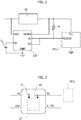
- Figure 1 a circuit such as, for instance, a microcontroller MCU is shown supplied with a voltage Vcc via a supply source SS such as a DC/DC converter or a low dropout regulator (LDO).
- a supply source SS such as a DC/DC converter or a low dropout regulator (LDO).
- a detector circuit designated ICD - for instance an (additional) integrated circuit or IC - may be provided supplied with the same supply voltage VDD applied to the supply source SS.
- a capacitor C D may facilitate time setting by an internal circuit, for instance, by providing a constant charge and discharge current through a pin CD, with the possibility of time adjustment by setting different capacitance values.
- the circuit ICD may be configured to be sensitive to the supply voltage VCC provided by the supply source SS to the microcontroller MCU (at a SENSE input) with the capability of detecting (for instance at respective inputs UV and OV coupled to the output from the source SS) the possible occurrence of under-voltage or over-voltage conditions in the microcontroller MCU.
- a pull-up resistor R can be provided in an open drain structure of the UV/OV outputs to facilitate obtaining logic "0" and "1" values.
- FIG. 1 - which, as noted, involves an additional IC such as ICD - may be configured in such a way that, when a fault occurs, one or more reset inputs RESETS in the circuit MCU are (always) triggered “low", so that OV events and UV events cannot be distinguished.
- One or more embodiments as exemplified herein facilitate providing a solution capable of detecting output over-voltage while at the same time giving a thermal warning indication.
- one or more embodiments are capable of:
- one or more embodiments facilitate avoiding the use SPI or other protocols, thus facilitating implementation in (very) simple devices such as a voltage regulator as exemplified at 10 in Figure 2 .
- the voltage regulator 10 may comprise an input pin Vs configured to receive an input voltage and an output pin Vo configured to provide a regulated supply voltage to an associated circuit supplied thereby such as a supplied microcontroller (MCU, for instance) or a sensitive load.
- MCU microcontroller
- Such an associated supplied circuit can be a distinct element from the embodiments of the circuit 10 and is shown in dashed line in Figure 2 .
- the voltage regulator 10 may comprise two pins RST and A TW configured to distinguish between under-voltage (UV) and over-voltage (OV) events and provide corresponding warning signals to an external microcontroller (such as MCU itself).
- UV under-voltage
- OV over-voltage
- RST may be for UV and A_TW for both OV and thermal warning, that is, an under voltage condition may be indicated through the RST pin and a same pin (that is A_TW) may be exploited both to indicate an output over-voltage (OV) condition and to provide a thermal warning.
- One or more embodiments are primarily concerned with arrangements which facilitate indicating such conditions at the pins of a device such as a voltage regulator 10 irrespective of how these conditions are revealed. Also, one or more embodiments may offer the advantage of being largely “transparent” to the methods/arrangements adopted for revealing under-voltage (UV) and over-voltage (OV) events as well as the temperature having reached an (upper) threshold.
- UV under-voltage
- OV over-voltage
- a same pin e.g. A TW
- a same pin can be "shared" for providing two different warning signals, with the capability of distinguishing these two events.
- a TW a same pin
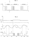
- FIG. 3 is indicative of a time interval TI where an over-voltage OV condition occurs with the signal at the pin A_TW (ordinate scale) exhibiting over time (abscissa scale t) a behavior including a sequence of bursts (1st burst, 2nd burst, ..., nth burst) superposed to a low logic level L.
- An over-temperature condition possibly occurring during TI may have no effect on the sequence of the burst signal.
- such possible principle of operation may facilitate taking into account the fact the over-voltage event may be regarded as having a priority in respect of an over-temperature event.
- OV over-voltage
- over temperature events if both over-voltage (OV) and over temperature events occur, OV will have a (first) priority on the A_TW pin, so that an over temperature event will not be detectable via the A_TW pin before the OV event disappears.
- the first drive mode of the warning output pin A TW adopted to indicate the first state (over-voltage) of the circuit 10 may include a different type of pulsed, and, more generally, alternating signal may be adopted in one or more embodiments.
- logic levels high (H) and low (L) can be possibly exchanged with each other.
- devoting the RST pin to a function different from reset information may not be advisable, for instance because the RST pin in a voltage regulator may be (directly) connected to the RST pin of a microcontroller configured to accept a specific signal on its input.
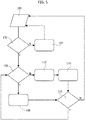
- the exemplary procedure discussed above for over-temperature and over-voltage management can be implemented as a state machine (FSM) 12 in the voltage regulator 10.
- FSM state machine
- the state machine 12 may be configured (in a manner known per se to those of skill in the art) to be sensitive to the voltage Vo and the temperature T and to operate according to the flow chart of Figure 5 .
- act 104 the A_TW pin is set/maintained to, e.g. high (H) and operation is looped back for a continuous check (act 102).
- an act 106 is performed in order to distinguish between an over-voltage and/or and over- temperature event.
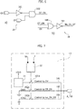
- burst signal patterns as exemplified in Figures 3 and 4 can be generated, in a manner known per se, for instance via a burst generator (14 in Figure 7 ) comprising a Schmitt trigger circuit coupled to a voltage V3V3 for charging and discharging an input capacitor, with, e.g. a D latch to achieve frequency division of the pulsed signal obtained thereby, for instance by using a delay may to obtain bursts of e.g. 3520 ⁇ S, 7040 ⁇ S from a 220 ⁇ S pulse width. For instance a delay may be used to generate three bursts and using a RC filter to reduce the small spike due to the delay.
- a burst generator (14 in Figure 7 ) comprising a Schmitt trigger circuit coupled to a voltage V3V3 for charging and discharging an input capacitor, with, e.g. a D latch to achieve frequency division of the pulsed signal obtained thereby, for instance by using a delay may to obtain bursts of e.g
- priority of over-voltage indication in respect of over-temperature can be achieved via circuits as exemplified in Figures 6 and 7 , which are suited to be incorporated to the state machine 12 and/or to be associated therewith.
- portion a) of Figure 6 is representative of an exemplary circuit 16 comprising inputs configured to receive signals OV and OT indicative (for instance, when "high") of an over-voltage condition and an over-temperature condition revealed, respectively. These signals are fed (after logical inversion at an inverter 161 gate, for the signal OV) to the inputs of an AND gate 162 which produces an output signal OT EN indicative (when "high") of over-temperature (only) occurring: in fact the output OT_EN from the AND gate 162 will be “high” as a result of OT being “high” (over-temperature revealed) and OV being “low” (no over-voltage revealed).
- the signal OT_EN may be applied to one of the inputs of an OR gate 180 receiving the signal OV on the other input, with the output from the OR gate 180 providing (after logical inversion at an inverter 181) an output signal No _OV_OT indicative of neither over-voltage nor over-temperature revealed.
- the output No_OV_OT from the inverter 181 will be "high” as a result of the output from the OR gate 180 being "low", that is with both of OV and OT “low” (no over-voltage and no over temperature revealed).
- Figure 7 is exemplary of a possible implementation of the A_TW pin as a wired-OR connection of three signal paths 101, 102, 103, namely:
- a burst signal always on, but without OV signal will not provide any indication to the A TW pin through the associated switch.
- a circuit (e.g., 10) comprises:
- the circuit comprises a warning output (e.g., A_TW) coupled to a warning signal generation network (e.g., 101, 101a, 14; 102, 102a, GND; 103, 103a, V3V3) controlled by the processing circuitry, the warning signal generation network configured to drive (e.g., 101a, 102a, 103a) the warning output in a first, a second and a third drive mode as a result of the processing circuitry being in said first, second and third state, respectively.
- a warning output e.g., A_TW
- a warning signal generation network e.g., 101, 101a, 14; 102, 102a, GND; 103, 103a, V3V3
- the warning signal generation network configured to drive (e.g., 101a, 102a, 103a) the warning output in a first, a second and a third drive mode as a result of the processing circuitry being in said first, second and third state, respectively.
- the processing circuitry may be configured to assume:
- said warning signal generation network is configured to drive said warning output in driving modes selected out of:
- the alternating signal may comprise a pulsed, optionally burst-like, signal.
- One or more embodiments comprises an alternating signal generator (e.g., Schmitt trigger-based as 14) supplied with a supply voltage (e.g., V3V3), and wherein said warning signal generation network may be configured to apply to the warning output said alternating signal, said first logic value and said second logic value by coupling (e.g. via the switches 101a, 102a, 103a) the warning output to said alternating signal generator, to ground and to said supply voltage.
- alternating signal generator e.g., Schmitt trigger-based as 14
- V3V3 supply voltage
- said warning signal generation network may be configured to apply to the warning output said alternating signal, said first logic value and said second logic value by coupling (e.g. via the switches 101a, 102a, 103a) the warning output to said alternating signal generator, to ground and to said supply voltage.
- said first, second and third mode may comprise said alternating signal (e.g., 1st burst, 2nd burst, ..., nth burst; 14), said first logic value (e.g., L; GND) and said second logic value (e.g., H; V3V3) applied to the warning output (e.g., A_TW), respectively.
- said alternating signal e.g., 1st burst, 2nd burst, ..., nth burst; 14
- said first logic value e.g., L; GND
- said second logic value e.g., H; V3V3 applied to the warning output (e.g., A_TW)
- the processing circuitry may be configured to assume the first state as a result of the voltage sensing signal reaching an upper voltage threshold (e.g., Vo_hth).
- an upper voltage threshold e.g., Vo_hth
- the circuit may comprise a further warning output (e.g., RST) coupled to the processing circuitry, the further warning output configured to receive a further warning signal indicative of the voltage sensing signal reaching a further threshold, optionally a lower threshold (e.g., with RST to indicate only a UV function, with the OV and OT functions indicated from A TW).
- RST further warning output
- a further threshold optionally a lower threshold (e.g., with RST to indicate only a UV function, with the OV and OT functions indicated from A TW).
- a device such as voltage regulated supply arrangement for a load, such as a microcontroller MCU
- a load such as a microcontroller MCU
- a device may comprise:
- a method may comprise:
Landscapes
- Engineering & Computer Science (AREA)
- Theoretical Computer Science (AREA)
- Physics & Mathematics (AREA)
- General Engineering & Computer Science (AREA)
- General Physics & Mathematics (AREA)
- Power Engineering (AREA)
- Computing Systems (AREA)
- Mathematical Physics (AREA)
- Business, Economics & Management (AREA)
- Emergency Management (AREA)
- Artificial Intelligence (AREA)
- Evolutionary Computation (AREA)
- Computer Hardware Design (AREA)
- Human Computer Interaction (AREA)
- Dc-Dc Converters (AREA)
- Alarm Systems (AREA)
Claims (8)
- Schaltung (10), umfassend:- einen Ausgangsknoten (Vo), der ausgestaltet ist, eine versorgte Last (MCU) mit einem regulierten Spannungssignal zu versorgen,- einen Verarbeitungsschaltkreis (12), der auf die regulierte Spannung an dem Ausgangsknoten (Vo) und auf eine Temperatur (T) der Schaltung (10) empfindlich reagiert, wobei die Verarbeitungsschaltung ausgestaltet ist, Spannung (OV) und Temperatur (OT) erfassende Signale bereitzustellen, die bezeichnend sind für die regulierte Spannung an dem Ausgangsknoten (Vo) und die Temperatur (T) der Schaltung (10), wobei der Verarbeitungsschaltkreis (12) ausgestaltet ist (16, 18, 100 bis 110), Folgendes anzunehmen:wobei die Schaltung (10) einen Warnausgang (A_TW) umfasst, der an ein Warnsignal-Erzeugungsnetzwerk (101, 101a, 14; 102, 102a, GND; 103, 103a, V3V3) gekoppelt ist, das von dem Verarbeitungsschaltkreis (12) gesteuert wird, wobei das Warnsignal-Erzeugungsnetzwerk ausgestaltet ist, den Warnausgang (A_TW) in einen ersten, einen zweiten und einen dritten Treibermodus zu treiben (101a, 102a, 103a), als ein Ergebnis des Verarbeitungsschaltkreises (12), der sich jeweils in dem ersten, zweiten und dritten Zustand befindet, dadurch gekennzeichnet, dass:- i) einen ersten Zustand (102, 106, 108) als ein Ergebnis des Spannung erfassenden Signals (OV), das eine Spannungsgrenze (Vo_hth) erreicht,- ii) einen zweiten Zustand (102, 106, 112, 114) als ein Ergebnis des Temperaturerfassungssignals (T), das eine Temperaturgrenze (Tth) erreicht,- iii) einen dritten Zustand (102, 104) als ein Ergebnis sowohl des Spannung (OV) als auch des Temperatur (OT) erfassenden Signals, die es nicht schaffen, die Grenzen (Vo_hth, Tth) zu erreichen,das Warnsignal-Erzeugungsnetzwerk (101, 101a, 14; 102, 102a, GND; 103, 103a, V3V3) ausgestaltet ist, den Warnausgang (A_TW) in Treibermodi zu treiben, ausgewählt aus:- einem Wechselsignal (1. Burst, 2. Burst, ..., n. Burst; 14), das auf den Warnausgang (A_TW) angewendet wird;- einem ersten Logikwert (L, GND), der auf den Warnausgang (A_TW) angewendet wird;- einem zweiten Logikwert (H, V3V3), der auf den Warnausgang (A_TW) angewendet wird; unddie Schaltung einen Wechselsignalgenerator (14) umfasst, der mit einer Versorgungsspannung (V3V3) versorgt wird, und wobei das Warnsignal-Erzeugungsnetzwerk (101, 101a, 14; 102, 102a, GND; 103, 103a, V3V3) ausgestaltet ist, auf den Warnausgang (A_TW) das Wechselsignal (1. Burst, 2. Burst, ..., n. Burst), den ersten Logikwert (L, GND) und den zweiten Logikwert (H, V3V3) anzuwenden, indem der Warnausgang (A_TW) an den Wechselsignalgenerator (14), an die Masse (GND) und an die Versorgungsspannung (V3V3) gekoppelt wird (101a, 102a, 103a).
- Schaltung (10) nach Anspruch 1, wobei der Verarbeitungsschaltkreis (12) ausgestaltet ist (16, 18, 100 bis 110), Folgendes anzunehmen:- den ersten Zustand (102, 106, 108) als ein Ergebnis des Spannung erfassenden Signals (OV), das die Spannungsgrenze (Vo_hth) erreicht, unabhängig davon, ob das Temperatur erfassende Signal (T) die Temperaturgrenze (Tth) erreicht, und/oder- den zweiten Zustand (102, 106, 112, 114) als ein Ergebnis des Temperatur erfassenden Signals (T), das die Temperaturgrenze (Tth) erreicht, wobei es das Spannung erfassende Signal (OV) nicht schafft, die Spannungsgrenze (Vo_hth) zu erreichen.
- Schaltung (10) nach Anspruch 1, wobei das Wechselsignal ein gepulstes, vorzugsweise Burst-ähnliches Signal (1. Burst, 2. Burst, ..., n. Burst) umfasst.
- Schaltung (10) nach einem der Ansprüche 1 bis 3, wobei der erste, zweite und dritte Modus das Wechselsignal (1. Burst, 2. Burst, ..., n. Burst; 14), den ersten Logikwert (L; GND) und den zweiten Logikwert (H; V3V3) umfassen, die jeweils auf den Warnausgang (A_TW) angewendet werden.
- Schaltung (10) nach einem der vorstehenden Ansprüche, wobei der Verarbeitungsschaltkreis (12) ausgestaltet ist (16, 18, 100 bis 110), den ersten Zustand (102, 106, 108) als ein Ergebnis des Spannung erfassenden Signals (OV), das eine obere Spannungsgrenze (Vo_hth) erreicht, anzunehmen.
- Schaltung (10) nach einem der vorstehenden Ansprüche, wobei die Schaltung einen weiteren Warnausgang (RST) umfasst, der an den Verarbeitungsschaltkreis (12) gekoppelt ist, wobei der weitere Warnausgang (RST) ausgestaltet ist, ein weiteres Warnsignal zu empfangen, das bezeichnend ist für das Spannung erfassende Signal (OV), das eine weitere Grenze erreicht, vorzugsweise eine untere Grenze (UV).
- Vorrichtung, umfassend:- eine Schaltung (10) nach einem der Ansprüche 1 bis 6,- eine versorgte Last (MCU), die an den Ausgangsknoten (Vo) der Schaltung (10) gekoppelt ist, um davon das regulierte Spannungssignal zu empfangen, und- eine Prozessorschaltung (MCU), die an den Warnausgang (A_TW) der Schaltung (10) gekoppelt ist, wobei die Prozessorschaltung (MCU) empfindlich auf Warnsignale reagiert, die von dem Warnausgang (A_TW) der Schaltung (10) bereitgestellt werden, der in den ersten, zweiten und dritten Treibermodus getrieben wird.
- Verfahren, umfassend:- Versorgen der versorgten Last (MCU) mit einem regulierten Spannungssignal (Vo) von einer Reglerschaltung (10),- Erfassen der regulierten Spannung (Vo), mit der die versorgte Last (MCU) versorgt wird, sowie einer Temperatur (T) der Reglerschaltung (10) und Bereitstellen von Spannung (OV) und Temperatur (OT) erfassenden Signalen, die bezeichnend sind für die regulierte Spannung und die Temperatur (T) der Reglerschaltung (10),- Bereitstellen einer Zustandsmaschine (12), die empfindlich auf die Spannung (OV) und Temperatur (OT) erfassenden Signale reagiert,- Wechseln der Zustandsmaschine in:- i) einen ersten Zustand (102, 106, 108) als ein Ergebnis des Spannung erfassenden Signals (OV), das eine Spannungsgrenze (Vo_hth) erreicht,- ii) einen zweiten Zustand (102, 106, 112, 114) als ein Ergebnis des Temperaturerfassungssignals (T), das eine Temperaturgrenze (Tth) erreicht,- iii) einen dritten Zustand (102, 104) als ein Ergebnis sowohl des Spannung (OV) als auch des Temperatur (OT) erfassenden Signals, die es nicht schaffen, die Grenzen (Vo_hth, Tth) zu erreichen,- Erzeugen eines Ausgangswarnsignals (A_TW) mit einem ersten, einem zweiten und einem dritten Ausgangstreibermodus als ein Ergebnis der Zustandsmaschine (12), die sich jeweils in dem ersten, zweiten und dritten Zustand befindet,wobei das Verfahren umfasst:Erzeugen des Ausgangswarnsignals (A_TW) an dem Warnausgang (A_TW) in Treibermodi, ausgewählt aus:- einem Wechselsignal (1. Burst, 2. Burst, ..., n. Burst; 14), das auf den Warnausgang (A_TW) angewendet wird;- einem ersten Logikwert (L, GND), der auf den Warnausgang (A_TW) angewendet wird;- einem zweiten Logikwert (H, V3V3), der auf den Warnausgang (A_TW) angewendet wird; undBereitstellen eines Wechselsignalgenerators (14), der mit einer Versorgungsspannung (V3V3) versorgt wird, und wobei das Erzeugen des Ausgangswarnsignals (A_TW) das Anwenden des Wechselsignals (1. Burst, 2. Burst, ..., n. Burst), des ersten Logikwerts (L, GND) und des zweiten Logikwerts (H, V3V3) auf den Warnausgang (A_TW) umfasst, indem der Warnausgang (A_TW) an den Wechselsignalgenerator (14), an die Masse (GND) und an die Versorgungsspannung (V3V3) gekoppelt wird (101a, 102a, 103a).
Applications Claiming Priority (1)
| Application Number | Priority Date | Filing Date | Title |
|---|---|---|---|
| IT102018000009272A IT201800009272A1 (it) | 2018-10-09 | 2018-10-09 | Circuito con avviso di condizioni di funzionamento critiche, dispositivo e procedimento corrispondenti |
Publications (2)
| Publication Number | Publication Date |
|---|---|
| EP3637571A1 EP3637571A1 (de) | 2020-04-15 |
| EP3637571B1 true EP3637571B1 (de) | 2021-04-28 |
Family
ID=64744877
Family Applications (1)
| Application Number | Title | Priority Date | Filing Date |
|---|---|---|---|
| EP19198276.8A Active EP3637571B1 (de) | 2018-10-09 | 2019-09-19 | Schaltung mit warnung vor kritischen betriebszuständen, entsprechende vorrichtung und verfahren |
Country Status (4)
| Country | Link |
|---|---|
| US (1) | US11211783B2 (de) |
| EP (1) | EP3637571B1 (de) |
| CN (2) | CN111030036B (de) |
| IT (1) | IT201800009272A1 (de) |
Families Citing this family (2)
| Publication number | Priority date | Publication date | Assignee | Title |
|---|---|---|---|---|
| IT201800009272A1 (it) * | 2018-10-09 | 2020-04-09 | St Microelectronics Srl | Circuito con avviso di condizioni di funzionamento critiche, dispositivo e procedimento corrispondenti |
| TWI887987B (zh) * | 2024-01-31 | 2025-06-21 | 新唐科技股份有限公司 | 警示產生電路 |
Family Cites Families (11)
| Publication number | Priority date | Publication date | Assignee | Title |
|---|---|---|---|---|
| US5648759A (en) * | 1994-02-02 | 1997-07-15 | National Semiconductor Corporation | Failsafe voltage regulator with warning signal driver |
| TW434991B (en) * | 1997-09-26 | 2001-05-16 | Hitachi Koki Kk | DC power source unit alarming before electrically powered tool is overheated and stopping power supply thereafter |
| US7155133B2 (en) * | 2002-02-12 | 2006-12-26 | Finisar Corporation | Avalanche photodiode controller circuit for fiber optics transceiver |
| JP5360002B2 (ja) * | 2010-06-28 | 2013-12-04 | 富士電機株式会社 | 半導体素子の駆動装置 |
| CN103460588B (zh) * | 2011-04-08 | 2016-05-25 | 富士电机株式会社 | 电力转换装置的控制装置 |
| CN102801184B (zh) * | 2011-05-24 | 2015-08-26 | 比亚迪股份有限公司 | 一种电池组管理系统 |
| JP6311228B2 (ja) * | 2013-07-05 | 2018-04-18 | 富士電機株式会社 | アラーム出力回路 |
| CN103532102B (zh) * | 2013-09-26 | 2017-10-17 | 昂宝电子(上海)有限公司 | 用于电源变换系统的过温保护和过压保护的系统和方法 |
| JP6244841B2 (ja) * | 2013-11-14 | 2017-12-13 | 富士通株式会社 | 直流レギュレータ、dc−dcコンバータおよび直流レギュレータの異常監視方法 |
| WO2016052011A1 (ja) * | 2014-09-29 | 2016-04-07 | 富士電機株式会社 | 半導体装置 |
| IT201800009272A1 (it) * | 2018-10-09 | 2020-04-09 | St Microelectronics Srl | Circuito con avviso di condizioni di funzionamento critiche, dispositivo e procedimento corrispondenti |
-
2018
- 2018-10-09 IT IT102018000009272A patent/IT201800009272A1/it unknown
-
2019
- 2019-09-19 EP EP19198276.8A patent/EP3637571B1/de active Active
- 2019-09-30 US US16/587,346 patent/US11211783B2/en active Active
- 2019-10-08 CN CN201910950396.9A patent/CN111030036B/zh active Active
- 2019-10-08 CN CN201921681965.6U patent/CN210898496U/zh not_active Withdrawn - After Issue
Non-Patent Citations (1)
| Title |
|---|
| None * |
Also Published As
| Publication number | Publication date |
|---|---|
| US11211783B2 (en) | 2021-12-28 |
| EP3637571A1 (de) | 2020-04-15 |
| IT201800009272A1 (it) | 2020-04-09 |
| CN111030036A (zh) | 2020-04-17 |
| CN111030036B (zh) | 2025-11-21 |
| US20200112164A1 (en) | 2020-04-09 |
| CN210898496U (zh) | 2020-06-30 |
Similar Documents
| Publication | Publication Date | Title |
|---|---|---|
| CN107482590B (zh) | 一种igbt模块的驱动与故障保护电路 | |
| US12322958B2 (en) | Electrostatic discharge (ESD) protection circuit with disable feature based on hot-plug condition detection | |
| US11296501B2 (en) | Integrated ESD event sense detector | |
| EP3637571B1 (de) | Schaltung mit warnung vor kritischen betriebszuständen, entsprechende vorrichtung und verfahren | |
| WO2021179128A1 (zh) | 电压攻击检测电路和芯片 | |
| EP0730347A2 (de) | Halbleitervorrichtung | |
| US5448441A (en) | Fault protection circuit for power switching device | |
| US7415647B2 (en) | Test mode for pin-limited devices | |
| US8826433B2 (en) | Security intrusion detection and response | |
| US20200285780A1 (en) | Cross domain voltage glitch detection circuit for enhancing chip security | |
| US12392822B2 (en) | Voltage glitch detectors | |
| US12493333B2 (en) | Power-on-reset request functionality in semiconductor devices and power management ICs | |
| US20180018012A1 (en) | Power control system | |
| US11563430B2 (en) | Transistor diagnostic circuit | |
| JP6702780B2 (ja) | 保護回路自己診断装置及び保護回路診断方法 | |
| JP3838722B2 (ja) | 強制動作機能付き制御回路を有する半導体装置 | |
| CN101859595B (zh) | 锁存装置及锁存方法 | |
| EP4560861A1 (de) | Treibervorrichtung und entsprechendes verfahren | |
| JP2857442B2 (ja) | 電源装置の低電圧検出装置 | |
| US12326465B2 (en) | Detector circuit | |
| US20250277827A1 (en) | Overvoltage and undervoltage detector | |
| JP2002091789A (ja) | ノイズ検出回路 | |
| CN120049367A (zh) | 驱动器装置和对应的方法 | |
| JPH0360215A (ja) | リセット回路 | |
| CN120433129A (zh) | 电源保护芯片及方法 |
Legal Events
| Date | Code | Title | Description |
|---|---|---|---|
| PUAI | Public reference made under article 153(3) epc to a published international application that has entered the european phase |
Free format text: ORIGINAL CODE: 0009012 |
|
| STAA | Information on the status of an ep patent application or granted ep patent |
Free format text: STATUS: THE APPLICATION HAS BEEN PUBLISHED |
|
| AK | Designated contracting states |
Kind code of ref document: A1 Designated state(s): AL AT BE BG CH CY CZ DE DK EE ES FI FR GB GR HR HU IE IS IT LI LT LU LV MC MK MT NL NO PL PT RO RS SE SI SK SM TR |
|
| AX | Request for extension of the european patent |
Extension state: BA ME |
|
| STAA | Information on the status of an ep patent application or granted ep patent |
Free format text: STATUS: REQUEST FOR EXAMINATION WAS MADE |
|
| 17P | Request for examination filed |
Effective date: 20200825 |
|
| RBV | Designated contracting states (corrected) |
Designated state(s): AL AT BE BG CH CY CZ DE DK EE ES FI FR GB GR HR HU IE IS IT LI LT LU LV MC MK MT NL NO PL PT RO RS SE SI SK SM TR |
|
| GRAP | Despatch of communication of intention to grant a patent |
Free format text: ORIGINAL CODE: EPIDOSNIGR1 |
|
| STAA | Information on the status of an ep patent application or granted ep patent |
Free format text: STATUS: GRANT OF PATENT IS INTENDED |
|
| INTG | Intention to grant announced |
Effective date: 20201215 |
|
| GRAS | Grant fee paid |
Free format text: ORIGINAL CODE: EPIDOSNIGR3 |
|
| GRAA | (expected) grant |
Free format text: ORIGINAL CODE: 0009210 |
|
| STAA | Information on the status of an ep patent application or granted ep patent |
Free format text: STATUS: THE PATENT HAS BEEN GRANTED |
|
| AK | Designated contracting states |
Kind code of ref document: B1 Designated state(s): AL AT BE BG CH CY CZ DE DK EE ES FI FR GB GR HR HU IE IS IT LI LT LU LV MC MK MT NL NO PL PT RO RS SE SI SK SM TR |
|
| REG | Reference to a national code |
Ref country code: GB Ref legal event code: FG4D |
|
| REG | Reference to a national code |
Ref country code: CH Ref legal event code: EP |
|
| REG | Reference to a national code |
Ref country code: DE Ref legal event code: R096 Ref document number: 602019004250 Country of ref document: DE |
|
| REG | Reference to a national code |
Ref country code: AT Ref legal event code: REF Ref document number: 1388209 Country of ref document: AT Kind code of ref document: T Effective date: 20210515 |
|
| REG | Reference to a national code |
Ref country code: IE Ref legal event code: FG4D |
|
| REG | Reference to a national code |
Ref country code: LT Ref legal event code: MG9D |
|
| REG | Reference to a national code |
Ref country code: AT Ref legal event code: MK05 Ref document number: 1388209 Country of ref document: AT Kind code of ref document: T Effective date: 20210428 |
|
| PG25 | Lapsed in a contracting state [announced via postgrant information from national office to epo] |
Ref country code: FI Free format text: LAPSE BECAUSE OF FAILURE TO SUBMIT A TRANSLATION OF THE DESCRIPTION OR TO PAY THE FEE WITHIN THE PRESCRIBED TIME-LIMIT Effective date: 20210428 Ref country code: LT Free format text: LAPSE BECAUSE OF FAILURE TO SUBMIT A TRANSLATION OF THE DESCRIPTION OR TO PAY THE FEE WITHIN THE PRESCRIBED TIME-LIMIT Effective date: 20210428 Ref country code: HR Free format text: LAPSE BECAUSE OF FAILURE TO SUBMIT A TRANSLATION OF THE DESCRIPTION OR TO PAY THE FEE WITHIN THE PRESCRIBED TIME-LIMIT Effective date: 20210428 Ref country code: NL Free format text: LAPSE BECAUSE OF FAILURE TO SUBMIT A TRANSLATION OF THE DESCRIPTION OR TO PAY THE FEE WITHIN THE PRESCRIBED TIME-LIMIT Effective date: 20210428 Ref country code: BG Free format text: LAPSE BECAUSE OF FAILURE TO SUBMIT A TRANSLATION OF THE DESCRIPTION OR TO PAY THE FEE WITHIN THE PRESCRIBED TIME-LIMIT Effective date: 20210728 Ref country code: AT Free format text: LAPSE BECAUSE OF FAILURE TO SUBMIT A TRANSLATION OF THE DESCRIPTION OR TO PAY THE FEE WITHIN THE PRESCRIBED TIME-LIMIT Effective date: 20210428 |
|
| PG25 | Lapsed in a contracting state [announced via postgrant information from national office to epo] |
Ref country code: RS Free format text: LAPSE BECAUSE OF FAILURE TO SUBMIT A TRANSLATION OF THE DESCRIPTION OR TO PAY THE FEE WITHIN THE PRESCRIBED TIME-LIMIT Effective date: 20210428 Ref country code: SE Free format text: LAPSE BECAUSE OF FAILURE TO SUBMIT A TRANSLATION OF THE DESCRIPTION OR TO PAY THE FEE WITHIN THE PRESCRIBED TIME-LIMIT Effective date: 20210428 Ref country code: PT Free format text: LAPSE BECAUSE OF FAILURE TO SUBMIT A TRANSLATION OF THE DESCRIPTION OR TO PAY THE FEE WITHIN THE PRESCRIBED TIME-LIMIT Effective date: 20210830 Ref country code: LV Free format text: LAPSE BECAUSE OF FAILURE TO SUBMIT A TRANSLATION OF THE DESCRIPTION OR TO PAY THE FEE WITHIN THE PRESCRIBED TIME-LIMIT Effective date: 20210428 Ref country code: NO Free format text: LAPSE BECAUSE OF FAILURE TO SUBMIT A TRANSLATION OF THE DESCRIPTION OR TO PAY THE FEE WITHIN THE PRESCRIBED TIME-LIMIT Effective date: 20210728 Ref country code: PL Free format text: LAPSE BECAUSE OF FAILURE TO SUBMIT A TRANSLATION OF THE DESCRIPTION OR TO PAY THE FEE WITHIN THE PRESCRIBED TIME-LIMIT Effective date: 20210428 Ref country code: IS Free format text: LAPSE BECAUSE OF FAILURE TO SUBMIT A TRANSLATION OF THE DESCRIPTION OR TO PAY THE FEE WITHIN THE PRESCRIBED TIME-LIMIT Effective date: 20210828 Ref country code: GR Free format text: LAPSE BECAUSE OF FAILURE TO SUBMIT A TRANSLATION OF THE DESCRIPTION OR TO PAY THE FEE WITHIN THE PRESCRIBED TIME-LIMIT Effective date: 20210729 |
|
| REG | Reference to a national code |
Ref country code: NL Ref legal event code: MP Effective date: 20210428 |
|
| PG25 | Lapsed in a contracting state [announced via postgrant information from national office to epo] |
Ref country code: EE Free format text: LAPSE BECAUSE OF FAILURE TO SUBMIT A TRANSLATION OF THE DESCRIPTION OR TO PAY THE FEE WITHIN THE PRESCRIBED TIME-LIMIT Effective date: 20210428 Ref country code: ES Free format text: LAPSE BECAUSE OF FAILURE TO SUBMIT A TRANSLATION OF THE DESCRIPTION OR TO PAY THE FEE WITHIN THE PRESCRIBED TIME-LIMIT Effective date: 20210428 Ref country code: SK Free format text: LAPSE BECAUSE OF FAILURE TO SUBMIT A TRANSLATION OF THE DESCRIPTION OR TO PAY THE FEE WITHIN THE PRESCRIBED TIME-LIMIT Effective date: 20210428 Ref country code: RO Free format text: LAPSE BECAUSE OF FAILURE TO SUBMIT A TRANSLATION OF THE DESCRIPTION OR TO PAY THE FEE WITHIN THE PRESCRIBED TIME-LIMIT Effective date: 20210428 Ref country code: SM Free format text: LAPSE BECAUSE OF FAILURE TO SUBMIT A TRANSLATION OF THE DESCRIPTION OR TO PAY THE FEE WITHIN THE PRESCRIBED TIME-LIMIT Effective date: 20210428 Ref country code: CZ Free format text: LAPSE BECAUSE OF FAILURE TO SUBMIT A TRANSLATION OF THE DESCRIPTION OR TO PAY THE FEE WITHIN THE PRESCRIBED TIME-LIMIT Effective date: 20210428 Ref country code: DK Free format text: LAPSE BECAUSE OF FAILURE TO SUBMIT A TRANSLATION OF THE DESCRIPTION OR TO PAY THE FEE WITHIN THE PRESCRIBED TIME-LIMIT Effective date: 20210428 |
|
| REG | Reference to a national code |
Ref country code: DE Ref legal event code: R097 Ref document number: 602019004250 Country of ref document: DE |
|
| PLBE | No opposition filed within time limit |
Free format text: ORIGINAL CODE: 0009261 |
|
| STAA | Information on the status of an ep patent application or granted ep patent |
Free format text: STATUS: NO OPPOSITION FILED WITHIN TIME LIMIT |
|
| 26N | No opposition filed |
Effective date: 20220131 |
|
| REG | Reference to a national code |
Ref country code: BE Ref legal event code: MM Effective date: 20210930 |
|
| PG25 | Lapsed in a contracting state [announced via postgrant information from national office to epo] |
Ref country code: IS Free format text: LAPSE BECAUSE OF FAILURE TO SUBMIT A TRANSLATION OF THE DESCRIPTION OR TO PAY THE FEE WITHIN THE PRESCRIBED TIME-LIMIT Effective date: 20210828 Ref country code: MC Free format text: LAPSE BECAUSE OF FAILURE TO SUBMIT A TRANSLATION OF THE DESCRIPTION OR TO PAY THE FEE WITHIN THE PRESCRIBED TIME-LIMIT Effective date: 20210428 Ref country code: AL Free format text: LAPSE BECAUSE OF FAILURE TO SUBMIT A TRANSLATION OF THE DESCRIPTION OR TO PAY THE FEE WITHIN THE PRESCRIBED TIME-LIMIT Effective date: 20210428 |
|
| PG25 | Lapsed in a contracting state [announced via postgrant information from national office to epo] |
Ref country code: LU Free format text: LAPSE BECAUSE OF NON-PAYMENT OF DUE FEES Effective date: 20210919 Ref country code: IT Free format text: LAPSE BECAUSE OF FAILURE TO SUBMIT A TRANSLATION OF THE DESCRIPTION OR TO PAY THE FEE WITHIN THE PRESCRIBED TIME-LIMIT Effective date: 20210428 Ref country code: IE Free format text: LAPSE BECAUSE OF NON-PAYMENT OF DUE FEES Effective date: 20210919 Ref country code: BE Free format text: LAPSE BECAUSE OF NON-PAYMENT OF DUE FEES Effective date: 20210930 |
|
| REG | Reference to a national code |
Ref country code: CH Ref legal event code: PL |
|
| PG25 | Lapsed in a contracting state [announced via postgrant information from national office to epo] |
Ref country code: CY Free format text: LAPSE BECAUSE OF FAILURE TO SUBMIT A TRANSLATION OF THE DESCRIPTION OR TO PAY THE FEE WITHIN THE PRESCRIBED TIME-LIMIT Effective date: 20210428 |
|
| PG25 | Lapsed in a contracting state [announced via postgrant information from national office to epo] |
Ref country code: LI Free format text: LAPSE BECAUSE OF NON-PAYMENT OF DUE FEES Effective date: 20220930 Ref country code: HU Free format text: LAPSE BECAUSE OF FAILURE TO SUBMIT A TRANSLATION OF THE DESCRIPTION OR TO PAY THE FEE WITHIN THE PRESCRIBED TIME-LIMIT; INVALID AB INITIO Effective date: 20190919 Ref country code: CH Free format text: LAPSE BECAUSE OF NON-PAYMENT OF DUE FEES Effective date: 20220930 |
|
| PG25 | Lapsed in a contracting state [announced via postgrant information from national office to epo] |
Ref country code: MK Free format text: LAPSE BECAUSE OF FAILURE TO SUBMIT A TRANSLATION OF THE DESCRIPTION OR TO PAY THE FEE WITHIN THE PRESCRIBED TIME-LIMIT Effective date: 20210428 |
|
| GBPC | Gb: european patent ceased through non-payment of renewal fee |
Effective date: 20230919 |
|
| PG25 | Lapsed in a contracting state [announced via postgrant information from national office to epo] |
Ref country code: GB Free format text: LAPSE BECAUSE OF NON-PAYMENT OF DUE FEES Effective date: 20230919 |
|
| PG25 | Lapsed in a contracting state [announced via postgrant information from national office to epo] |
Ref country code: GB Free format text: LAPSE BECAUSE OF NON-PAYMENT OF DUE FEES Effective date: 20230919 |
|
| PG25 | Lapsed in a contracting state [announced via postgrant information from national office to epo] |
Ref country code: MT Free format text: LAPSE BECAUSE OF FAILURE TO SUBMIT A TRANSLATION OF THE DESCRIPTION OR TO PAY THE FEE WITHIN THE PRESCRIBED TIME-LIMIT Effective date: 20210428 |
|
| PGFP | Annual fee paid to national office [announced via postgrant information from national office to epo] |
Ref country code: DE Payment date: 20250820 Year of fee payment: 7 |
|
| PGFP | Annual fee paid to national office [announced via postgrant information from national office to epo] |
Ref country code: FR Payment date: 20250820 Year of fee payment: 7 |
|
| PG25 | Lapsed in a contracting state [announced via postgrant information from national office to epo] |
Ref country code: TR Free format text: LAPSE BECAUSE OF FAILURE TO SUBMIT A TRANSLATION OF THE DESCRIPTION OR TO PAY THE FEE WITHIN THE PRESCRIBED TIME-LIMIT Effective date: 20210428 |