EP3631536B1 - Height-modulated diffractive master plate and method of manufacturing thereof - Google Patents
Height-modulated diffractive master plate and method of manufacturing thereof Download PDFInfo
- Publication number
- EP3631536B1 EP3631536B1 EP18809747.1A EP18809747A EP3631536B1 EP 3631536 B1 EP3631536 B1 EP 3631536B1 EP 18809747 A EP18809747 A EP 18809747A EP 3631536 B1 EP3631536 B1 EP 3631536B1
- Authority
- EP
- European Patent Office
- Prior art keywords
- height
- surface profile
- profile
- filling material
- substrate
- Prior art date
- Legal status (The legal status is an assumption and is not a legal conclusion. Google has not performed a legal analysis and makes no representation as to the accuracy of the status listed.)
- Active
Links
Images

Classifications
-
- G—PHYSICS
- G02—OPTICS
- G02B—OPTICAL ELEMENTS, SYSTEMS OR APPARATUS
- G02B5/00—Optical elements other than lenses
- G02B5/18—Diffraction gratings
- G02B5/1847—Manufacturing methods
- G02B5/1857—Manufacturing methods using exposure or etching means, e.g. holography, photolithography, exposure to electron or ion beams
-
- B—PERFORMING OPERATIONS; TRANSPORTING
- B29—WORKING OF PLASTICS; WORKING OF SUBSTANCES IN A PLASTIC STATE IN GENERAL
- B29D—PRODUCING PARTICULAR ARTICLES FROM PLASTICS OR FROM SUBSTANCES IN A PLASTIC STATE
- B29D11/00—Producing optical elements, e.g. lenses or prisms
-
- B—PERFORMING OPERATIONS; TRANSPORTING
- B29—WORKING OF PLASTICS; WORKING OF SUBSTANCES IN A PLASTIC STATE IN GENERAL
- B29D—PRODUCING PARTICULAR ARTICLES FROM PLASTICS OR FROM SUBSTANCES IN A PLASTIC STATE
- B29D11/00—Producing optical elements, e.g. lenses or prisms
- B29D11/0074—Production of other optical elements not provided for in B29D11/00009- B29D11/0073
- B29D11/00769—Producing diffraction gratings
-
- G—PHYSICS
- G02—OPTICS
- G02B—OPTICAL ELEMENTS, SYSTEMS OR APPARATUS
- G02B27/00—Optical systems or apparatus not provided for by any of the groups G02B1/00 - G02B26/00, G02B30/00
- G02B27/01—Head-up displays
- G02B27/017—Head mounted
- G02B27/0172—Head mounted characterised by optical features
-
- G—PHYSICS
- G02—OPTICS
- G02B—OPTICAL ELEMENTS, SYSTEMS OR APPARATUS
- G02B27/00—Optical systems or apparatus not provided for by any of the groups G02B1/00 - G02B26/00, G02B30/00
- G02B27/42—Diffraction optics, i.e. systems including a diffractive element being designed for providing a diffractive effect
- G02B27/44—Grating systems; Zone plate systems
-
- G—PHYSICS
- G02—OPTICS
- G02B—OPTICAL ELEMENTS, SYSTEMS OR APPARATUS
- G02B5/00—Optical elements other than lenses
- G02B5/18—Diffraction gratings
- G02B5/1828—Diffraction gratings having means for producing variable diffraction
-
- G—PHYSICS
- G02—OPTICS
- G02B—OPTICAL ELEMENTS, SYSTEMS OR APPARATUS
- G02B5/00—Optical elements other than lenses
- G02B5/18—Diffraction gratings
- G02B5/1847—Manufacturing methods
- G02B5/1852—Manufacturing methods using mechanical means, e.g. ruling with diamond tool, moulding
-
- G—PHYSICS
- G03—PHOTOGRAPHY; CINEMATOGRAPHY; ANALOGOUS TECHNIQUES USING WAVES OTHER THAN OPTICAL WAVES; ELECTROGRAPHY; HOLOGRAPHY
- G03F—PHOTOMECHANICAL PRODUCTION OF TEXTURED OR PATTERNED SURFACES, e.g. FOR PRINTING, FOR PROCESSING OF SEMICONDUCTOR DEVICES; MATERIALS THEREFOR; ORIGINALS THEREFOR; APPARATUS SPECIALLY ADAPTED THEREFOR
- G03F7/00—Photomechanical, e.g. photolithographic, production of textured or patterned surfaces, e.g. printing surfaces; Materials therefor, e.g. comprising photoresists; Apparatus specially adapted therefor
- G03F7/0005—Production of optical devices or components in so far as characterised by the lithographic processes or materials used therefor
-
- G—PHYSICS
- G02—OPTICS
- G02B—OPTICAL ELEMENTS, SYSTEMS OR APPARATUS
- G02B27/00—Optical systems or apparatus not provided for by any of the groups G02B1/00 - G02B26/00, G02B30/00
- G02B27/01—Head-up displays
- G02B27/0101—Head-up displays characterised by optical features
- G02B2027/0123—Head-up displays characterised by optical features comprising devices increasing the field of view
- G02B2027/0125—Field-of-view increase by wavefront division
-
- G—PHYSICS
- G02—OPTICS
- G02B—OPTICAL ELEMENTS, SYSTEMS OR APPARATUS
- G02B27/00—Optical systems or apparatus not provided for by any of the groups G02B1/00 - G02B26/00, G02B30/00
- G02B27/01—Head-up displays
- G02B27/017—Head mounted
- G02B2027/0178—Eyeglass type
Definitions
- the invention relates to manufacturing of micro- and nanostructures for optical purposes.
- the invention relates to manufacturing a master plate for producing diffractive gratings, which can be used for example in display applications, such as near-to-eye displays.
- NEDs Near-to-eye displays
- HUDs head-up displays
- Gratings are needed as in-coupling gratings, which couple an image from an image source to a wave guide, as out-coupling gratings, which produce the final viewable image for the user, and as exit pupil expanders (EPEs), which increase the size of the displays exit pupil.
- EPEs exit pupil expanders
- the quality and characteristics of the gratings determine the quality of resulting image.
- Grayscale lithography provides a way to fabricate structures with varying structure height.
- the sidewalls are typically rounded and not entirely vertical.
- the control of grayscale-lithographic processes is challenging.
- direct lithography and etch processes are very difficult to tune to provide high accuracy in vertical dimension, especially when features of the grating, i.e. ridges and grooves, contain several aspect ratios and depths over a large surface area. It is also difficult to achieve perfectly vertical sidewalls of features using these methods in combination with height modulation.
- Stamping techniques require a high-quality master plate and a stamp manufactured using the master plate, whereby the main challenge is in the manufacturing of the master.
- Fabrication of height-modulated structures is generally done by repeating fabrication cycles in which one height is defined within one cycle. This requires several exposures with high precision alignment, see for example C. David, "Fabrication of stair-case profiles with high aspect ratios for blazed diffractive optical elements ", Microelectronic Engineering, 53 (2000 ). Because of the complexity of the method, the yield is low. This method provides good control over the vertical sidewalls but suffers from complexity and required precision. Moreover, overlay exposure requires a lateral placement accuracy in nanometer level, and any deviations from optimal causes losses in optical performance. Further relevant prior art can be found in GB 1362418 A and CA2214927 A1 .
- the method according to the invention comprises fabricating a master plate for producing diffractive structures by
- the removal step comprises using a physical mask layer on top of the filling, as explained below in more detail.
- the invention offers significant benefits.
- the invention solves the problem of low quality structures of direct lithographic methods involving height-modulation due to low contrast and resulting rounded sidewalls.
- the sidewalls are defined by the substrate, which is manufactured for example by binary processing leading to very well defined vertical sidewalls.
- Binary processing is very well known and easy to control.
- the following uneven material removal step is introduced to achieve the height modulation.
- the vertical sidewalls of the features are defined by the binary structure and the height differences of the features by the filling layer.
- a combination of these two leads to precisely controllable profile shape and height that is difficult to achieve by other methods. Similar advantages apply to e.g. triangular initial surface profiles.
- the invention allows for producing master plates capable of further producing gratings with variable diffraction efficiency.
- the present method allows for lateral variation of diffraction efficiency using height modulation, and also using fill factor modulation, in combination with high-quality diffractive structures.
- the uneven partial removal of the filling layer comprises grayscale lithographic removal.
- This covers any method where different exposure doses result in different dissolving rates of the exposed filling material and therefore different heights in the filling layer.
- the term covers both so-called direct write methods, where the exposure of the material, and therefore the thickness of material removed, is controlled directly by the exposure source used, such as laser, electron or x-ray source, and methods using an optical mask and a light source with essentially even brightness and typically laterally broad exposure.
- the exposure may be carried out using photons (light) or electrons (optical or electron beam exposure, respectively).
- a combination or variation of direct write and optical mask methods is also possible.
- the partial removal of the filling layer can be carried out, for example, using a photolithographic etching method directly after application of a suitable resist layer as the the filling layer. This makes the process very quick and robust.
- the materials of the substrate and the resist layer and the etching method are chosen to be selective such that only the resist layer is modified and in particular the vertical sidewalls of the binary features remain intact.
- the modulation in the resist layer is transferred to the substrate material by dry etching.
- the uneven mask comprises a physical mask in the form of a mask layer applied on the filling material.
- the mask layer has a laterally varying height, whose height profile corresponds to the desired modulation of the plate. After that, applying laterally uniform etching process or other suitable removal process results in the replication of the height profile to the filling material.
- the mask layer may comprise the same material as the filling layer or any other material etchable together with the filling layer.
- removal using a physical mask layer covers any removal methods that utilize an additional sacrificial mask layer on top of the filling layer, wherein the sacrificial mask layer has an effect on the local thickness of remaining filling layer.
- a resist layer is applied on a filling layer as explained above and a grayscale exposure is applied either by using direct write or an optical mask with varying transmission intensities. This height variation in the resist layer is then transferred to the filling layer by dry etching or wet etching.
- the removal process results in a surface profile with at least two distinct segments of different modulation heights.
- the boundary of the segments can be discrete, whereby there is a stepwise height difference between the segments.
- the grating may comprise for example 2 - 500 segments having different height characteristics.
- a lateral height gradient can be produced by photolithography, for example, using direct writing, an optical gradient mask or a physical gradient mask.
- the gradient may be a linear gradient or a non-linear gradient.
- the surface profile is entirely filled with the filling material before the removal is initiated. This allows for utilization of the entire height of the profile for modulation and also ensures complete filling of the profile.
- the substrate can be planarized with the filling material.
- the surface profile comprises a periodic pattern of a plurality of features having rectangular or triangular cross-section and elongated form.
- the pattern may be a line grating pattern capable of producing a one-dimensional linear grating.
- two-dimensional gratings is possible, with e.g. a two-dimensional array of dot features, whereby the initial surface profile of the substrate and the final surface profile of the master plate are doubly periodic. A combination of these is also possible.
- the binary surface profile comprises fill factor modulation, which using the present method is maintained and replicated to the resulting surface profile of the plate.
- the substrate is manufactured by providing a substrate plate and removing material from the substrate plate, for example by electron beam lithography, or adding material to the plate, for example by nanoimprinting, to produce the binary surface profile thereon.
- the height-modulated surface profile comprises vertical sidewalls and feature tops, which are entirely defined by the substrate, and gap bottoms which are entirely defined by the filling material.
- the required area of the master plate is at least 1 cm 2 , such as 2 - 500 cm 2 , which is readily achievable with the present process.
- the period of the master grating is typically 10 ⁇ m or less, in particular 1 ⁇ m or less, such as 200 - 800 nm.
- binary surface profile herein essentially means a surface with a relief structure consisting of two heights. In a line grating the possible heights are defined by tops of ridges and bottoms of grooves adjacent to the ridges. The profile therefore consists of cross-sectionally essentially rectangular surface features (with entirely vertical sidewalls). Binary surface profile is used an example in the following discussion and drawings, although other profiles are also possible, as discussed above.
- Filling with filling material covers full filling and partial filling.
- Planarization means full filling such that enough filling material is provided on the surface profile to embed the binary features of the profile so that a planar surface made of the filling material is formed.
- Partial removal of filling material means that at least some thickness of filling material is left on at least some location of the substrate.
- Height modulation refers to variation of dimension of grating features in the normal direction of the substrate. For example, in the case of a line grating, height is measured from the bottom of a groove adjacent to a ridge to the top of the ridge.
- a height-modulated master plate thus comprises at least two lateral segments, either in one or two dimensions, with different feature heights between the regions.
- fill factor refers to the proportion of grating structure material to surrounding material (e.g. air or other solid material) within a grating period. In the typical case of rectangular grating lines, this equals to the proportion of line width to period width. Consequently, “fill factor modulation” refers to variation of fill factor in the lateral dimensions of the grating, i.e. between periods of the periodic structure.
- the present method combines highly anisotropic high resolution binary processing of the substrate and height modulation by applying a physical mask layer having an uneven height profile on the filling material.
- Lower lateral resolution grayscale lithography of the added filling material is carried out.
- it enables better control of the high-resolution vertical features and the sidewall profiles in comparison with direct grayscale lithography, where vertical sidewalls are difficult to achieve.
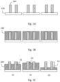
- Figs. 1A - 1C illustrate the first basic example not falling under the claims, which uses a grayscale lithography step to produce the height modulation on the binary substrate.
- a binary structure with a possible fill factor modulation (not shown here) is fabricated using for example optical, electron beam lithography, embossing or nanoimprint lithography.
- the structure comprises a base plate 12A and binary elements 14A extending from the base plate 12A. At this point all the elements 14A have the same height.
- the base plate 12A and binary elements 14A may comprise a unitary piece of single material or be made of different materials.
- the elements 14A may comprise polymer added on an inorganic or polymeric base plate 12A.
- the substrate can be polymeric or inorganic unitary entity into which the features are processed by lithographic methods.
- Fill factor modulation including line width modulation, gap width modulation or both, can also be included. This layer is referred to as grating layer.
- the binary structure 12A, 14A is coated with an electron beam or optical lithography resist material, to at least partially fill the gaps between the elements 14A, and typically so that the grating layer is fully covered with the resist material and the surface of the structure is planarized with a fill layer 16A.
- a grayscale lithography is performed to the fill layer 16A .
- This kind of an overlay grayscale exposure results in different development speeds caused by different exposure doses and different heights arising from the surface.
- regions S1, S2, S3 of different element heights h1, h2, h3, respectively, are formed, defined by the thickness of the fill layer 16A' at each region.
- the grayscale lithography may be carried out using direct writing with a laser, for example, according to an exposure scheme corresponding to the desired modulation or using an optical mask producing an illumination pattern having simultaneously a plurality of distinct regions of different intensities corresponding to the desired modulation.
- a continuous gradient may be formed.
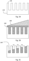
- Figs. 2A - 2C illustrate an embodiment of the invention, which uses a physical mask to produce the height modulation.
- a binary structure 12B is fabricated using in a similar manner as described above with reference to the first basic embodiment.
- the binary structure is planarized with a fill layer 16B as described above.
- variable-height mask layer 18B is applied by any lithography method.
- significantly lower lateral resolution is required in comparison with the grating layer resolution.
- a dry or wet etch method is used to transfer modulation of the mask layer 18B into the fill layer 16B'. Again, due to high selectivity between the fill layer 16B, 16B' and the grating layer 12B, high control over grating profile is retained.
- a gradient mask is used, but, like in the previous example, the mask can comprise distinct regions of different heights.
- a combination of these approaches can also be used, depending on the desired height characteristics of the resulting master plate.
- the embodiment allows for different diffraction efficiencies in a single high-quality diffractive structure as the vertical sidewall characteristics of the structure are defined by the substrate and height characteristics are defined by the masked etch process. Due to high selectivity between filling layer 16A, 16B and grating layer 12A-B, 14A-B, the full control over the grating line profiles is retained even if the etch process was isotropic.
- the binary surface profile of the substrate can be a resist structure or it can be transferred to the substrate by wet or dry etching.
- the structure is then typically coated with an electron beam or optical lithography resist which has selectivity with respect to the binary structure.
- the period of the grating is typically a fraction of minimum lateral dimensions of the mask zones, i.e. the segments have a considerably higher size with respect to the period.
- the mask zones which determine diffraction efficiency segments in the final product, can have dimensions of 10 ⁇ m or more, typically 1 mm or more, whereas the grating period is typically 10 ⁇ m or less, in particular 1 ⁇ m or less.
- the substrate in all embodiments can be a standard silicon wafer or SiO 2 wafer, for example. Also, any other rigid or flexible substrate that can be applied in optical or electron beam lithography can be used.
- the binary surface profile i.e., a relief structure
- this layer can be any thin film that can be processed in dry or wet etching methods.
- the surface profile can be formed using an optical or electron beam resist, in which case the binary structure can be fabricated by optical or electron beam exposure and developed to the layer.
- the resist material can also be etched in order to fabricate the binary structure.
- the filling layer can be an optical or electron beam resist. It can be applied by spin-coating, spray coating or dip-coating to mention some examples.
- the filling layer can be deposited by using physical vapor deposition (PVD) or chemical vapor deposition (CVD) or atomic layer deposition (ALD).
- PVD physical vapor deposition
- CVD chemical vapor deposition
- ALD atomic layer deposition
- This can be for example a metal oxide such as Al 2 O 3 or TiO 2 or other. It can also be SiO 2 .
- the filling layer has high selectivity with respect to the binary surface profile material, taking into account the removal method used (e.g. high etch selectivity). In other words, the filling material has to be selected so that during partial removal of this layer, the original binary structure remains intact.
- the present height modulation can take place in the periodic dimension of the surface profile, as illustrated in the drawings. However, it is not excluded that it additionally or instead of that, takes place in the perpendicular dimension of the grating, for example along the grating lines of a line gradient.
- the present method is also equally applicable to two-dimensional gratings having periodicity in two different directions.
- the present master plate can be used to produce diffractive optical elements having laterally non-constant diffraction efficiency for various needs.
- the plate can be used to produce large elements, typically having an area of 1 cm 2 or more, for example for NEDs or HUDs.
- Variable diffraction efficiency provides advantages in in-coupling gratings, exit pupil expanders and/or out-coupling gratings of diffractive waveguide displays, such as smart glasses and virtual reality and augmented reality displays.
- the master plate produced using the present method can be used in stamping processes, which are known per se in the art of producing diffractive gratings.
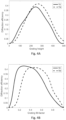
- Figs. 4A and 4B show how the diffraction efficiency of the first transmission order of a dielectric binary grating can be modulated using height and fill-factor modulation. Numerical results were obtained with the Fourier modal method (also known as rigorous coupled wave analysis). The binary grating resides on an interface between air and a glass substrate having refractive index of 2.0, the grating period is 500 nm, fill factor 0.5, and the grating is made of the same material as the substrate. The grating is illuminated with a plane wave with 450 nm free space wavelength at normal incidence. Results are shown for both transverse electric (TE) and transverse magnetic polarizations (TM). In Fig. 4A , the grating fill factor is 0.5 and in Fig. 4B , the grating height is 250 nm.
- TE transverse electric
- TM transverse magnetic polarizations
Landscapes
- Physics & Mathematics (AREA)
- Engineering & Computer Science (AREA)
- General Physics & Mathematics (AREA)
- Optics & Photonics (AREA)
- Manufacturing & Machinery (AREA)
- Health & Medical Sciences (AREA)
- Ophthalmology & Optometry (AREA)
- Mechanical Engineering (AREA)
- Diffracting Gratings Or Hologram Optical Elements (AREA)
- Exposure And Positioning Against Photoresist Photosensitive Materials (AREA)
- Exposure Of Semiconductors, Excluding Electron Or Ion Beam Exposure (AREA)
Applications Claiming Priority (2)
| Application Number | Priority Date | Filing Date | Title |
|---|---|---|---|
| FI20175506A FI128574B (en) | 2017-06-02 | 2017-06-02 | Height-modulated diffractive master plate and process for its manufacture |
| PCT/FI2018/050379 WO2018220270A1 (en) | 2017-06-02 | 2018-05-18 | Height-modulated diffractive master plate and method of manufacturing thereof |
Publications (4)
| Publication Number | Publication Date |
|---|---|
| EP3631536A1 EP3631536A1 (en) | 2020-04-08 |
| EP3631536A4 EP3631536A4 (en) | 2021-03-10 |
| EP3631536B1 true EP3631536B1 (en) | 2024-08-07 |
| EP3631536C0 EP3631536C0 (en) | 2024-08-07 |
Family
ID=64455234
Family Applications (1)
| Application Number | Title | Priority Date | Filing Date |
|---|---|---|---|
| EP18809747.1A Active EP3631536B1 (en) | 2017-06-02 | 2018-05-18 | Height-modulated diffractive master plate and method of manufacturing thereof |
Country Status (6)
| Country | Link |
|---|---|
| US (1) | US11391870B2 (enExample) |
| EP (1) | EP3631536B1 (enExample) |
| JP (1) | JP7379775B2 (enExample) |
| CN (1) | CN111033325B (enExample) |
| FI (1) | FI128574B (enExample) |
| WO (1) | WO2018220270A1 (enExample) |
Families Citing this family (10)
| Publication number | Priority date | Publication date | Assignee | Title |
|---|---|---|---|---|
| US10690821B1 (en) * | 2018-12-14 | 2020-06-23 | Applied Materials, Inc. | Methods of producing slanted gratings |
| US11669012B2 (en) * | 2020-02-21 | 2023-06-06 | Applied Materials, Inc. | Maskless lithography method to fabricate topographic substrate |
| CN115698778A (zh) * | 2020-06-03 | 2023-02-03 | 应用材料公司 | 波导光栅的梯度密封 |
| CN115803686A (zh) * | 2020-06-25 | 2023-03-14 | 奇跃公司 | 用于头戴式显示器的目镜及其制造方法 |
| US11709422B2 (en) | 2020-09-17 | 2023-07-25 | Meta Platforms Technologies, Llc | Gray-tone lithography for precise control of grating etch depth |
| US20220082739A1 (en) * | 2020-09-17 | 2022-03-17 | Facebook Technologies, Llc | Techniques for manufacturing variable etch depth gratings using gray-tone lithography |
| FI130396B (fi) * | 2020-09-23 | 2023-08-10 | Dispelix Oy | Optinen aaltojohde lisätyn todellisuuden näyttölaitteeseen |
| US12259552B2 (en) * | 2020-12-17 | 2025-03-25 | Google Llc | Spatial variance along waveguide incoupler |
| US12442961B1 (en) | 2021-07-23 | 2025-10-14 | Apple Inc. | Methods of forming holographic gratings for optical systems |
| EP4609237A1 (en) * | 2022-10-27 | 2025-09-03 | Applied Materials, Inc. | Inkjet gradient index material to modulate grating diffraction efficiency |
Family Cites Families (20)
| Publication number | Priority date | Publication date | Assignee | Title |
|---|---|---|---|---|
| US3669673A (en) * | 1970-10-23 | 1972-06-13 | Rca Corp | Recording of a continuous tone focused image on a diffraction grating |
| US3944420A (en) * | 1974-05-22 | 1976-03-16 | Rca Corporation | Generation of permanent phase holograms and relief patterns in durable media by chemical etching |
| JPS52125348A (en) * | 1976-05-13 | 1977-10-21 | Rca Corp | Composite focused hologram record |
| JPH1078667A (ja) * | 1996-09-04 | 1998-03-24 | Ebara Corp | 微細加工方法 |
| CA2197706A1 (en) * | 1997-02-14 | 1998-08-14 | Peter Ehbets | Method of fabricating apodized phase mask |
| JPH1131863A (ja) * | 1997-07-11 | 1999-02-02 | Hitachi Ltd | 回折格子の製造方法及びそれを用いて製造した半導体レーザ及びそれを用いた光応用システム |
| CA2214927A1 (en) | 1997-10-31 | 1999-04-30 | Pin Long | Methods for making phase masks with spatial variable first order efficiency for fiber bragg grating fabrication |
| US6534221B2 (en) | 1998-03-28 | 2003-03-18 | Gray Scale Technologies, Inc. | Method for fabricating continuous space variant attenuating lithography mask for fabrication of devices with three-dimensional structures and microelectronics |
| JP2002189112A (ja) | 2000-12-22 | 2002-07-05 | Canon Inc | 回折光学素子の製造方法、回折光学素子の製造方法によって製造したことを特徴とする回折光学素子製造用金型、回折光学素子、および該回折光学素子を有する光学系、光学機器、露光装置、デバイス製造方法、デバイス |
| CN1797199A (zh) * | 2004-12-22 | 2006-07-05 | 中国科学院光电技术研究所 | 移动灰阶掩模微纳结构成形方法 |
| JP2007212575A (ja) * | 2006-02-07 | 2007-08-23 | Ricoh Co Ltd | 光回折素子、光線走査方法、光線走査装置及び画像形成装置 |
| US8317321B2 (en) * | 2007-07-03 | 2012-11-27 | Pixeloptics, Inc. | Multifocal lens with a diffractive optical power region |
| US9791623B2 (en) * | 2009-11-30 | 2017-10-17 | Board Of Regents, The University Of Texas System | Multilevel leaky-mode resonant optical devices |
| US9400432B2 (en) * | 2010-10-28 | 2016-07-26 | National University Of Singapore | Lithography method and apparatus |
| CN103901520B (zh) * | 2014-04-23 | 2016-07-06 | 中国科学技术大学 | 一种顶角90°三角形槽阶梯光栅的制作方法 |
| US20160033784A1 (en) | 2014-07-30 | 2016-02-04 | Tapani Levola | Optical Components |
| JPWO2016185602A1 (ja) * | 2015-05-21 | 2018-03-08 | ナルックス株式会社 | 回折光学素子 |
| US9885870B2 (en) * | 2016-04-25 | 2018-02-06 | Microsoft Technology Licensing, Llc | Diffractive optical elements with analog modulations and switching |
| CN105785493B (zh) * | 2016-05-09 | 2019-01-22 | 深圳市华星光电技术有限公司 | 金属光栅偏光片及其制作方法 |
| US10649141B1 (en) * | 2018-04-23 | 2020-05-12 | Facebook Technologies, Llc | Gratings with variable etch heights for waveguide displays |
-
2017
- 2017-06-02 FI FI20175506A patent/FI128574B/en active IP Right Grant
-
2018
- 2018-05-18 US US16/618,178 patent/US11391870B2/en active Active
- 2018-05-18 WO PCT/FI2018/050379 patent/WO2018220270A1/en not_active Ceased
- 2018-05-18 EP EP18809747.1A patent/EP3631536B1/en active Active
- 2018-05-18 CN CN201880038493.4A patent/CN111033325B/zh active Active
- 2018-05-18 JP JP2019566818A patent/JP7379775B2/ja active Active
Also Published As
| Publication number | Publication date |
|---|---|
| US11391870B2 (en) | 2022-07-19 |
| FI128574B (en) | 2020-08-14 |
| EP3631536A4 (en) | 2021-03-10 |
| CN111033325A (zh) | 2020-04-17 |
| JP2020522026A (ja) | 2020-07-27 |
| CN111033325B (zh) | 2022-01-11 |
| JP7379775B2 (ja) | 2023-11-15 |
| WO2018220270A1 (en) | 2018-12-06 |
| EP3631536C0 (en) | 2024-08-07 |
| FI20175506A1 (en) | 2018-12-03 |
| US20200110206A1 (en) | 2020-04-09 |
| EP3631536A1 (en) | 2020-04-08 |
Similar Documents
| Publication | Publication Date | Title |
|---|---|---|
| EP3631536B1 (en) | Height-modulated diffractive master plate and method of manufacturing thereof | |
| US11513268B2 (en) | Method of manufacturing a variable efficiency diffractive grating and a diffractive grating | |
| EP3631538B1 (en) | Method of manufacturing a master plate | |
| US10274823B2 (en) | Microlithographic fabrication of structures | |
| JP7143974B2 (ja) | 高さ調整された光回折格子を製造する方法 | |
| EP3631534B1 (en) | Method of manufacturing a diffractive grating |
Legal Events
| Date | Code | Title | Description |
|---|---|---|---|
| STAA | Information on the status of an ep patent application or granted ep patent |
Free format text: STATUS: THE INTERNATIONAL PUBLICATION HAS BEEN MADE |
|
| PUAI | Public reference made under article 153(3) epc to a published international application that has entered the european phase |
Free format text: ORIGINAL CODE: 0009012 |
|
| STAA | Information on the status of an ep patent application or granted ep patent |
Free format text: STATUS: REQUEST FOR EXAMINATION WAS MADE |
|
| 17P | Request for examination filed |
Effective date: 20191128 |
|
| AK | Designated contracting states |
Kind code of ref document: A1 Designated state(s): AL AT BE BG CH CY CZ DE DK EE ES FI FR GB GR HR HU IE IS IT LI LT LU LV MC MK MT NL NO PL PT RO RS SE SI SK SM TR |
|
| AX | Request for extension of the european patent |
Extension state: BA ME |
|
| DAV | Request for validation of the european patent (deleted) | ||
| DAX | Request for extension of the european patent (deleted) | ||
| A4 | Supplementary search report drawn up and despatched |
Effective date: 20210208 |
|
| RIC1 | Information provided on ipc code assigned before grant |
Ipc: B29D 11/00 20060101ALI20210202BHEP Ipc: G02B 5/18 20060101AFI20210202BHEP Ipc: G02B 27/44 20060101ALI20210202BHEP Ipc: G02B 27/00 20060101ALI20210202BHEP Ipc: G02B 27/01 20060101ALI20210202BHEP Ipc: G03F 7/00 20060101ALI20210202BHEP |
|
| STAA | Information on the status of an ep patent application or granted ep patent |
Free format text: STATUS: EXAMINATION IS IN PROGRESS |
|
| 17Q | First examination report despatched |
Effective date: 20230526 |
|
| GRAP | Despatch of communication of intention to grant a patent |
Free format text: ORIGINAL CODE: EPIDOSNIGR1 |
|
| STAA | Information on the status of an ep patent application or granted ep patent |
Free format text: STATUS: GRANT OF PATENT IS INTENDED |
|
| GRAJ | Information related to disapproval of communication of intention to grant by the applicant or resumption of examination proceedings by the epo deleted |
Free format text: ORIGINAL CODE: EPIDOSDIGR1 |
|
| STAA | Information on the status of an ep patent application or granted ep patent |
Free format text: STATUS: EXAMINATION IS IN PROGRESS |
|
| INTG | Intention to grant announced |
Effective date: 20240131 |
|
| GRAP | Despatch of communication of intention to grant a patent |
Free format text: ORIGINAL CODE: EPIDOSNIGR1 |
|
| STAA | Information on the status of an ep patent application or granted ep patent |
Free format text: STATUS: GRANT OF PATENT IS INTENDED |
|
| INTC | Intention to grant announced (deleted) | ||
| INTG | Intention to grant announced |
Effective date: 20240305 |
|
| GRAJ | Information related to disapproval of communication of intention to grant by the applicant or resumption of examination proceedings by the epo deleted |
Free format text: ORIGINAL CODE: EPIDOSDIGR1 |
|
| STAA | Information on the status of an ep patent application or granted ep patent |
Free format text: STATUS: EXAMINATION IS IN PROGRESS |
|
| GRAP | Despatch of communication of intention to grant a patent |
Free format text: ORIGINAL CODE: EPIDOSNIGR1 |
|
| STAA | Information on the status of an ep patent application or granted ep patent |
Free format text: STATUS: GRANT OF PATENT IS INTENDED |
|
| GRAS | Grant fee paid |
Free format text: ORIGINAL CODE: EPIDOSNIGR3 |
|
| GRAA | (expected) grant |
Free format text: ORIGINAL CODE: 0009210 |
|
| STAA | Information on the status of an ep patent application or granted ep patent |
Free format text: STATUS: THE PATENT HAS BEEN GRANTED |
|
| INTC | Intention to grant announced (deleted) | ||
| INTG | Intention to grant announced |
Effective date: 20240621 |
|
| AK | Designated contracting states |
Kind code of ref document: B1 Designated state(s): AL AT BE BG CH CY CZ DE DK EE ES FI FR GB GR HR HU IE IS IT LI LT LU LV MC MK MT NL NO PL PT RO RS SE SI SK SM TR |
|
| REG | Reference to a national code |
Ref country code: GB Ref legal event code: FG4D |
|
| REG | Reference to a national code |
Ref country code: CH Ref legal event code: EP |
|
| REG | Reference to a national code |
Ref country code: IE Ref legal event code: FG4D |
|
| REG | Reference to a national code |
Ref country code: DE Ref legal event code: R096 Ref document number: 602018072847 Country of ref document: DE |
|
| U01 | Request for unitary effect filed |
Effective date: 20240826 |
|
| U07 | Unitary effect registered |
Designated state(s): AT BE BG DE DK EE FI FR IT LT LU LV MT NL PT RO SE SI Effective date: 20240903 |
|
| PG25 | Lapsed in a contracting state [announced via postgrant information from national office to epo] |
Ref country code: NO Free format text: LAPSE BECAUSE OF FAILURE TO SUBMIT A TRANSLATION OF THE DESCRIPTION OR TO PAY THE FEE WITHIN THE PRESCRIBED TIME-LIMIT Effective date: 20241107 |
|
| PG25 | Lapsed in a contracting state [announced via postgrant information from national office to epo] |
Ref country code: PL Free format text: LAPSE BECAUSE OF FAILURE TO SUBMIT A TRANSLATION OF THE DESCRIPTION OR TO PAY THE FEE WITHIN THE PRESCRIBED TIME-LIMIT Effective date: 20240807 Ref country code: GR Free format text: LAPSE BECAUSE OF FAILURE TO SUBMIT A TRANSLATION OF THE DESCRIPTION OR TO PAY THE FEE WITHIN THE PRESCRIBED TIME-LIMIT Effective date: 20241108 |
|
| PG25 | Lapsed in a contracting state [announced via postgrant information from national office to epo] |
Ref country code: IS Free format text: LAPSE BECAUSE OF FAILURE TO SUBMIT A TRANSLATION OF THE DESCRIPTION OR TO PAY THE FEE WITHIN THE PRESCRIBED TIME-LIMIT Effective date: 20241207 |
|
| PG25 | Lapsed in a contracting state [announced via postgrant information from national office to epo] |
Ref country code: HR Free format text: LAPSE BECAUSE OF FAILURE TO SUBMIT A TRANSLATION OF THE DESCRIPTION OR TO PAY THE FEE WITHIN THE PRESCRIBED TIME-LIMIT Effective date: 20240807 |
|
| PG25 | Lapsed in a contracting state [announced via postgrant information from national office to epo] |
Ref country code: RS Free format text: LAPSE BECAUSE OF FAILURE TO SUBMIT A TRANSLATION OF THE DESCRIPTION OR TO PAY THE FEE WITHIN THE PRESCRIBED TIME-LIMIT Effective date: 20241107 Ref country code: ES Free format text: LAPSE BECAUSE OF FAILURE TO SUBMIT A TRANSLATION OF THE DESCRIPTION OR TO PAY THE FEE WITHIN THE PRESCRIBED TIME-LIMIT Effective date: 20240807 |
|
| PG25 | Lapsed in a contracting state [announced via postgrant information from national office to epo] |
Ref country code: RS Free format text: LAPSE BECAUSE OF FAILURE TO SUBMIT A TRANSLATION OF THE DESCRIPTION OR TO PAY THE FEE WITHIN THE PRESCRIBED TIME-LIMIT Effective date: 20241107 Ref country code: PL Free format text: LAPSE BECAUSE OF FAILURE TO SUBMIT A TRANSLATION OF THE DESCRIPTION OR TO PAY THE FEE WITHIN THE PRESCRIBED TIME-LIMIT Effective date: 20240807 Ref country code: NO Free format text: LAPSE BECAUSE OF FAILURE TO SUBMIT A TRANSLATION OF THE DESCRIPTION OR TO PAY THE FEE WITHIN THE PRESCRIBED TIME-LIMIT Effective date: 20241107 Ref country code: IS Free format text: LAPSE BECAUSE OF FAILURE TO SUBMIT A TRANSLATION OF THE DESCRIPTION OR TO PAY THE FEE WITHIN THE PRESCRIBED TIME-LIMIT Effective date: 20241207 Ref country code: HR Free format text: LAPSE BECAUSE OF FAILURE TO SUBMIT A TRANSLATION OF THE DESCRIPTION OR TO PAY THE FEE WITHIN THE PRESCRIBED TIME-LIMIT Effective date: 20240807 Ref country code: GR Free format text: LAPSE BECAUSE OF FAILURE TO SUBMIT A TRANSLATION OF THE DESCRIPTION OR TO PAY THE FEE WITHIN THE PRESCRIBED TIME-LIMIT Effective date: 20241108 Ref country code: ES Free format text: LAPSE BECAUSE OF FAILURE TO SUBMIT A TRANSLATION OF THE DESCRIPTION OR TO PAY THE FEE WITHIN THE PRESCRIBED TIME-LIMIT Effective date: 20240807 |
|
| PG25 | Lapsed in a contracting state [announced via postgrant information from national office to epo] |
Ref country code: SM Free format text: LAPSE BECAUSE OF FAILURE TO SUBMIT A TRANSLATION OF THE DESCRIPTION OR TO PAY THE FEE WITHIN THE PRESCRIBED TIME-LIMIT Effective date: 20240807 |
|
| PG25 | Lapsed in a contracting state [announced via postgrant information from national office to epo] |
Ref country code: CZ Free format text: LAPSE BECAUSE OF FAILURE TO SUBMIT A TRANSLATION OF THE DESCRIPTION OR TO PAY THE FEE WITHIN THE PRESCRIBED TIME-LIMIT Effective date: 20240807 |
|
| PG25 | Lapsed in a contracting state [announced via postgrant information from national office to epo] |
Ref country code: SK Free format text: LAPSE BECAUSE OF FAILURE TO SUBMIT A TRANSLATION OF THE DESCRIPTION OR TO PAY THE FEE WITHIN THE PRESCRIBED TIME-LIMIT Effective date: 20240807 |
|
| PLBE | No opposition filed within time limit |
Free format text: ORIGINAL CODE: 0009261 |
|
| STAA | Information on the status of an ep patent application or granted ep patent |
Free format text: STATUS: NO OPPOSITION FILED WITHIN TIME LIMIT |
|
| U20 | Renewal fee for the european patent with unitary effect paid |
Year of fee payment: 8 Effective date: 20250527 |
|
| PGFP | Annual fee paid to national office [announced via postgrant information from national office to epo] |
Ref country code: GB Payment date: 20250527 Year of fee payment: 8 |
|
| 26N | No opposition filed |
Effective date: 20250508 |