EP3629573B1 - Schneller bilderfassungssensor mit pixel-binning - Google Patents
Schneller bilderfassungssensor mit pixel-binning Download PDFInfo
- Publication number
- EP3629573B1 EP3629573B1 EP19199960.6A EP19199960A EP3629573B1 EP 3629573 B1 EP3629573 B1 EP 3629573B1 EP 19199960 A EP19199960 A EP 19199960A EP 3629573 B1 EP3629573 B1 EP 3629573B1
- Authority
- EP
- European Patent Office
- Prior art keywords
- read
- pixels
- pixel
- coupled
- transistor
- Prior art date
- Legal status (The legal status is an assumption and is not a legal conclusion. Google has not performed a legal analysis and makes no representation as to the accuracy of the status listed.)
- Active
Links
Images


Classifications
-
- H—ELECTRICITY
- H04—ELECTRIC COMMUNICATION TECHNIQUE
- H04N—PICTORIAL COMMUNICATION, e.g. TELEVISION
- H04N25/00—Circuitry of solid-state image sensors [SSIS]; Control thereof
- H04N25/40—Extracting pixel data from image sensors by controlling scanning circuits, e.g. by modifying the number of pixels sampled or to be sampled
- H04N25/46—Extracting pixel data from image sensors by controlling scanning circuits, e.g. by modifying the number of pixels sampled or to be sampled by combining or binning pixels
-
- H—ELECTRICITY
- H04—ELECTRIC COMMUNICATION TECHNIQUE
- H04N—PICTORIAL COMMUNICATION, e.g. TELEVISION
- H04N25/00—Circuitry of solid-state image sensors [SSIS]; Control thereof
-
- H—ELECTRICITY
- H04—ELECTRIC COMMUNICATION TECHNIQUE
- H04N—PICTORIAL COMMUNICATION, e.g. TELEVISION
- H04N25/00—Circuitry of solid-state image sensors [SSIS]; Control thereof
- H04N25/70—SSIS architectures; Circuits associated therewith
- H04N25/76—Addressed sensors, e.g. MOS or CMOS sensors
- H04N25/77—Pixel circuitry, e.g. memories, A/D converters, pixel amplifiers, shared circuits or shared components
- H04N25/778—Pixel circuitry, e.g. memories, A/D converters, pixel amplifiers, shared circuits or shared components comprising amplifiers shared between a plurality of pixels, i.e. at least one part of the amplifier must be on the sensor array itself
-
- H—ELECTRICITY
- H04—ELECTRIC COMMUNICATION TECHNIQUE
- H04N—PICTORIAL COMMUNICATION, e.g. TELEVISION
- H04N25/00—Circuitry of solid-state image sensors [SSIS]; Control thereof
- H04N25/70—SSIS architectures; Circuits associated therewith
- H04N25/76—Addressed sensors, e.g. MOS or CMOS sensors
- H04N25/78—Readout circuits for addressed sensors, e.g. output amplifiers or A/D converters
Definitions
- the invention relates to the field of fast imaging, that is to say fast image sensors, or “burst” imagers, making it possible to capture images at rates ranging from a thousand to billions. frames per second.
- the pixels of high speed imagers have large dimensions, for example between approximately 10 ⁇ 10 ⁇ m 2 and 50 ⁇ 50 ⁇ m 2 .
- Each pixel has a photodetector and a read circuit associated with the photodetector.
- the photodetector corresponds for example to a photodiode.
- the read circuit corresponds for example to a capacitive transimpedance amplifier (or CTIA for “Capacitive Translmpedance Amplifier”).
- CTIA Capacitive Translmpedance Amplifier
- the read circuit is connected to a storage element which can correspond to a storage capacitor when the signal delivered by the read circuit is then processed in an analog manner.
- the storage element can also form part of an analog-to-digital converter (or ADC for “Analog Digital Converter”) which comprises at least one capacitive load as input ensuring temporary storage of the signal delivered by the read circuit and received by ADC. It is also possible to have at least one capacitor present between the read circuit and the ADC, for example in a circuit of the sampler-and-hold type, and also forming a storage element.
- the figure 1 schematically represents an exemplary embodiment of a pixel 10 of a fast image sensor.
- This pixel 10 comprises a photodetector corresponding here to a photodiode 12.
- the photodiode 12 is connected to a read circuit of the pixel comprising here a CTIA formed by an operational amplifier 14, an integration capacitor 16 coupling the output of amplifier 14 to a first input of amplifier 14, and a reset switch 18 connected in parallel to capacitor 16
- Photodiode 12 is connected to the first input of amplifier 14.
- a reference electric potential “Vref” is applied to a second input of amplifier 14.
- the output of amplifier 14 is connected to input d a circuit 20 which may be an ADC or an analog storage circuit.
- the input of circuit 20 has a capacitive load 19 which performs a temporary storage or sampling function of the signal delivered by amplifier 14.
- a “binning” of pixels that is to say a grouping of pixels.
- Each group of pixels called a macro-pixel, is in this case considered to deliver a single image information item at the output of the macro-pixel.
- the photodetectors of a macro-pixel deliver signals to the input of a circuit for reading only one of the pixels of the macro-pixel so that this reading circuit reads all the signals received from the photodetectors.
- This grouping of pixels makes it possible to increase the image capture rate since the information delivered by the pixels of the same macro-pixel are considered not as several pieces of information to be processed individually one after the other but as a single piece of information to be processed. treat. For example, if such a grouping is carried out by forming macro-pixels composed of two pixels, the reading speed of the sensor can be multiplied by two. In addition, the total capture area of a macro-pixel is larger than the individual area of each pixel, which contributes to the increase in the capture rate due to the greater sensitivity provided by the larger area. macro-pixel capture for each information to be processed.
- the figure 2 schematically represents an exemplary embodiment of two pixels 10.1 and 10.2, each formed by components similar to those of pixel 10 previously described in connection with the figure 1 , and grouped to form a single macro-pixel.
- the photodiodes 12.1, 12.2 are connected to the input of one of the read circuits reading the currents delivered by the two photodiodes 12.1, 12.2.
- This connection is obtained via the closing of a switch 22 making it possible to connect the photodiode 12.2 of the second pixel 10.2 to the input of the CTIA of the first pixel 10.1.
- the output of the CTIA of the second pixel 10.2 is disconnected from the ADC 20.2 associated with the second pixel 10.2 by opening another switch 21 interposed between the output of the CTIA of the second pixel 10.2 and the ADC 20.2.
- the output of the CTIA is indeed electrically connected to the ADC 20.1 associated with the first pixel 10.1.
- the CTIA of the first pixel 10.1 reads the signals delivered by the photodiodes 12.1, 12.2 of the two pixels 10.1, 10.2.
- the two photodiodes 12.1 and 12.2 each deliver a current at the input of the CTIA of the first pixel 10.1 which reads the sum of these two currents.
- the signal delivered at the output of the CTIA of the first pixel 10.1 is stored and converted by the ADC 20.1 associated with the first pixel 10.1.
- the operating speed of the storage elements is slightly impacted by these groupings, because the ADCs will process fewer pixels more quickly.
- this grouping of pixels requires the reading circuits to operate more quickly compared to the initial configuration where all the pixel reading circuits operated in parallel, in order to achieve the desired image capture rate. Now, this faster operation of the read circuits can pose a problem with regard to the charging of the capacitors forming the storage elements, the available time possibly not being sufficient for, for each group of pixels, the storage circuit. reading that is active can sufficiently charge the capacity of the storage element associated with the group of pixels.
- An aim of the present invention is to provide a fast image sensor which does not have the drawbacks described above, that is to say which can be configured to achieve a grouping of pixels (“binning”) compatible with a rate. high capture, and this without oversizing the components of the read circuits with respect to a single sensor operating without grouping of pixels.
- the reading circuits of the pixels grouped together in the same macro-pixel are coupled, or connected, in parallel and behave like a larger resulting reading circuit, realizing the reading of the sum of the photodetection signals delivered by the photodetectors.
- the read signals delivered at the output of the read circuits are then sent to the input of a single storage element.
- the active amplification in the read circuits, the fan-outs, or output currents, of the read circuits are cumulative, which makes it possible to rapidly charge the capacities of the storage elements, and this without having to oversize the components of the read circuits compared to a similar image sensor in which the pixels are not clustered.
- a macro-pixel designates several pixels grouped together such that, during a reading of the pixels, the reading signals delivered by the reading circuits of these pixels are considered together as a single global information representative of the light signal captured at the level of the whole macro-pixel.
- the amplification element is qualified as “active” because it is capable of generating a current.
- Coupled is used in this document to denote a link or a connection, preferably electrical, which can be direct or indirect between two elements coupled to one another, that is to say with or without an element. intermediate interposed between the two elements coupled to each other.
- Each macro-pixel is formed from at least two pixels, and advantageously comprises a number of pixels of between approximately 2 and 10 pixels.
- the read circuits of the image sensor can be similar to each other.
- a storage element here corresponds to a component or an electronic circuit providing a storage function, whether temporary or not.
- the main function of the storage element can be a storage function, or another function, such as for example an analog-to-digital conversion function or a temporary sampling function when the conversion element corresponds to a capacitive load. of an ADC.
- each read circuit is coupled to an input of a storage element different from those to which the outputs of the read circuits of the other pixels are connected, and the pixel grouping means comprise switches for connecting the read circuits interposed between the outputs of the reading circuits and the inputs of the storage elements.
- the pixel grouping means comprise switches for connecting the read circuits interposed between the outputs of the reading circuits and the inputs of the storage elements.
- the senor can operate in a standard manner, that is to say without performing any grouping of pixels, each pixel being linked to the storage element associated with it.
- the pixel array may be disposed in a first substrate, and the storage elements may be disposed in a separate second substrate and superimposed on the first substrate.
- the read circuits can be arranged in the first substrate, for example within the pixels, or in the second substrate.
- Each pixel can have dimensions between approximately 10 x 10 ⁇ m 2 and 50 x 50 ⁇ m 2 .
- the photodetection signals can correspond to photodetection currents, and the output signals of the read circuits, called read signals, can correspond to read voltages.
- Each storage element can correspond to a capacitive load of an analog / digital converter (ADC), or to a storage capacitor, or to a capacitor present between the read circuit and the ADC.
- ADC analog / digital converter
- Each photodetector can include at least one photodiode.
- each read circuit may include at least one capacitive transimpedance amplifier forming the active amplification element of the read circuit.
- the connection switch of the integration capacitor of a single read circuit can be in the closed position, the other switch (s) of connection of the integration capacitor of the other read circuit (s) of the macro-pixel which may be in the open position, in order to couple only one integration capacitor of one of the read circuits in parallel of the operational amplifiers of the circuits macro-pixel reading.
- each storage element can be coupled to a transistor mounted as a common drain, the gate of which is coupled to the capacitance of the storage element and the drain of which is coupled to a current source.
- each read circuit can be associated with several sub-pixels configured to detect ranges of different wavelengths and intended to be read successively by the read circuit, the read circuit possibly comprising several transfer transistors. each comprising a first source or drain electrode coupled to the photodetector of one of the sub-pixels associated with the read circuit.
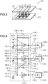
- FIG 3 schematically represents an image sensor 100 according to a particular embodiment.
- the sensor 100 corresponds to a fast image sensor, or “burst” imager.
- the sensor 100 is produced in the form of a 3D (three-dimensional) electronic circuit and comprises a matrix of pixels 110 formed in a first substrate 102 and electronic processing circuits produced in the first substrate 102 and in a second substrate 104 distinct from the first substrate 102 and superimposed on the first substrate 102.
- the sensor 100 comprises means for grouping pixels, or “binning”, making it possible to form, from the pixels 110 of the matrix, macro-pixels, in order to increase the image capture rate of the sensor 100 ( however, generating images each comprising fewer pixels than the images obtained when the pixels are not grouped into macro-pixels).
- the figure 4 represents three pixels 110, referenced 110.1, 110.2 and 110.3, of the sensor 100 grouped together within a single macro-pixel, according to a first embodiment.
- Each of the three pixels 110 includes a photodetector 112 (referenced 112.1, 112.2 and 112.3 on the figure 4 ), corresponding for example to a photodiode.
- Each of the three pixels 110 also includes a read circuit 160 (references 160.1 - 160.3 on the figure 4 ). Each read circuit 160 is produced within one of the pixels.
- the read circuits 160 comprise active amplification elements corresponding to CTIAs each comprising an operational amplifier (AOP) 114 (referenced 114.1, 114.2 and 114.3 on the figure 4 ), an integration capacity 116 (referenced 116.1, 116.2 and 116.3 on the figure 4 ) and a reset switch 118 (referenced 118.1, 118.2 and 118.3 on the figure 4 ).
- AOP operational amplifier
- the photodetectors 112 and the read circuits 160 which are associated with them are here produced in the first substrate 102.
- the output of each of the read circuits 160 is coupled to a storage element corresponding here to a capacitive load 119 (referenced 119.1, 119.2 and 119.3) of an ADC 120 (referenced 120.1, 120.2 and 120.3).
- the ADCs 120 are here produced in the second substrate 104.
- First electrical connections 122 electrically couple the inputs of read circuits 160 to one another, and second electrical links 124 electrically couple the outputs of read circuits 160 to one another. Read circuits 160 are thus coupled in parallel with one another.
- Switches 126 (referenced 126.1, 126.2 and 126.3 on the figure 4 ) for connecting the integration capacitors 116 are interposed between the first electrodes of the integration capacitors 116 and the inputs of the amplifiers 114, and switches 128 (referenced 128.1 to 128.4 on the figure 4 ) for connecting the pixels 110 are interposed on the first and second electrical connections 122, 124, between the pixels 110.
- the switches 126.2, 126.3 are in the open position, and the switch 126.1 is in the closed position so that only the integration capacitor 116.1 is coupled in parallel to the three amplifiers 114, the other two integration capacitors 116.2 and 116.3 being disconnected reading circuits 160.
- the three pixels 110.1, 110.2 and 110.3 form a single macro-pixel, the switches 128.1 to 128.4 being in the closed position in order to connect in parallel the reading circuits 160 of the three pixels 110.1, 110.2 and 110.3.
- the three photodetectors 112.1, 112.2, 112.3 deliver photodetection currents to the inputs of the three operational amplifiers 114.1, 114.2, 114.3.
- the three amplifiers 114.1, 114.2, 114.3 of the three read circuits 160 cooperate to read the photodetection signals delivered by the photodiodes 112 of the three pixels 110.1, 110.2 and 110.3.
- each of the read circuits 160 of the pixels 110 is coupled to the input of one of the ADCs 120.
- switches 130 referenced 130.1, 130.2 and 130.3 on the figure 4 ) for connecting the read circuits 160 are interposed between the output of each read circuit 160 and the input of each ADC 120.
- the two switches 130.2 and 130.3 are in the open position and the switch 130.1 is in the closed position so that only the ADC 120.1 receives as input the read signals delivered by the read circuits 160 of the pixels 110.
- the sensor 100 comprises other electronic processing elements to which the outputs of the ADCs 120, or more generally the outputs of the read circuits 160, are coupled. These electronic elements are not described in detail here, nor for the other embodiments.
- the storage elements to which the outputs of the pixel read circuits are coupled correspond to capacitive loads of the ADCs.
- these storage elements can correspond to electronic circuits different from these ADCs, but comprising at least one capacitor.
- Such storage circuits are for example described in the document "In-Pixel Storage Techniques for CMOS Burst-Mode Ultra-High-Speed Imagers ”by L. Wu et al., 2017,: Conference: 2017 International Image Sensors Workshop, Hiroshima, Japan .
- the storage elements to which the outputs of the pixel read circuits are coupled may correspond to temporary storage capacities of circuits of the sampler-and-hold type.
- the storage elements can correspond to storage capacities for a sensor operating in analog.
- each macro-pixel can have a number of pixels between approximately 2 and 10.
- the read circuit 160 of each pixel 110 comprises a CTIA.
- the figure 5 represents two pixels 110.1, 110.2 of the sensor 100 according to an example useful for understanding the invention and in which the read circuits of the pixels 110 do not include a CTIA but correspond to 3T type circuits (with three transistors).
- the transistors of the read circuits correspond for example to field effect transistors, advantageously MOSFETs.
- each read circuit comprises a first transistor 140 (referenced 140.1 and 140.2 on the figure 5 ) making it possible to reset the pixels 110, via the application of the reset voltage V RAZ to the terminals of the photodetectors 112 when the first transistors 140 are in the on state.
- Each read circuit also includes a second transistor 142 (referenced 142.1 and 142.2 on the figure 5 ) mounted as a common drain (and also called “source follower" in English) whose gate forming the input of the read circuit is coupled to the photodetector 112 associated with the read circuit. Due to the fact that the two pixels 110.1, 110.2 are grouped here to form a macro-pixel, the gates of the second transistors 142.1 and 142.2 are electrically coupled to each other by the electrical link 122 and the switch 128, thus coupling one to the other the inputs of the two reading circuits of the pixels 110.1, 110.2.
- the switch 128 makes it possible to pool the photodetectors 112 or to separate them, depending on the desired operating mode (binning or not).
- Each read circuit also includes a third transistor 144 (referenced 144.1 and 144.2 on the figure 5 ) configured to connect the read circuit to the output line 146 and comprising a first source or drain electrode (drain in the case of a third NMOS transistor 144 as in the example of figure 5 ) coupled to the second transistor 142 (connected to the source of the second NMOS transistor 142 on the example of figure 5 ), and a second source or drain electrode (source on the example of figure 5 ) forming the output of the read circuit and which is coupled to the output line 146 of the pixel matrix.
- the read circuits of the two pixels 110.1, 110.2 deliver on line 146 the read signals delivered by the second transistors 142 when the third transistors 144 are in the on state.
- the outputs of the reading circuits of two pixels 110.1, 110.2 are electrically coupled to one another so as to output a single image information item per macro-pixel.
- the outputs of the read circuits of the two pixels 110.1, 110.2 are coupled, via line 146, to the input of a storage element corresponding here to a storage capacitor 148.
- a transistor 149 allows the bias to be biased.
- a read circuit which imposes a read voltage in the storage capacitor 148 through the output line 146.
- placing the read circuits in parallel here does not make it possible to sum the currents of the signals delivered by the second transistors 142 because it is the transistor 149 present at the bottom of each column which imposes the read voltage applied to the input of the storage circuit corresponding to the storage capacitor 148.
- the figure 7 represents three pixels 110, referenced 110.1, 110.2 and 110.3, of the sensor 100 grouped together within a single macro-pixel, according to a second embodiment.
- each pixel 110 includes all the elements previously described in connection with the first embodiment shown in the figure. figure 4 .
- the read circuit (bearing the reference 160 on the figure 7 ) of each pixel 110 an active amplification element different from that previously described in the first embodiment.
- the figure 8 shows a first embodiment of such a pixel 110 comprising an active amplification element which does not correspond to a CTIA.
- the active amplification element of the read circuit 160 of the pixel 110 is formed by the transistor 142 mounted as a common drain and a current source 162, for example formed by a transistor, which is coupled to the source of transistor 142.
- the transistor 142 is of type P. Thanks to this active amplification element, during a grouping of pixels, the output currents of the grouped pixels accumulate and are stored in the same storage element.
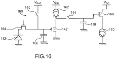
- the figure 9 represents a second exemplary embodiment of such a pixel 110 comprising an active amplification element which does not correspond to a CTIA.
- the active amplification element of the read circuit 160 of the pixel 110 is formed by the transistor 142 mounted as a common drain and a current source 162, for example formed by a transistor, which is coupled to the source of transistor 142, as in the first example of figure 8 .
- this pixel 110 comprises a transfer transistor 164 interposed between the gate of transistor 142 and the input of read circuit 160, as well as a storage node coupled to the gate of transistor 142 and forming a capacitor 166 coupled in parallel with the transistor 140.
- each storage element is coupled to a transistor 168 mounted as a common drain, the gate of which is coupled to the capacitor 119 of the storage element.
- the drain of transistor 168 is coupled to a current source 170.
- Transistor 168 and current source 170 form a second active amplifying element. Such a configuration is shown in the figure 10 .
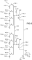
- the figure 6 represents eight pixels 110.1 - 110.8 of the sensor 100 according to another example useful for understanding the invention, in which the read circuits of the pixels 110 correspond to circuits of the 1.75 T type (1.75 transistors).
- the Transistors of the read circuits correspond for example to field effect transistors, advantageously MOSFETs.
- the pixels 110.1 - 110.4 are associated with a first read circuit, and the pixels 110.5 - 110.8 are associated with a second read circuit.
- Each pixel 110 includes a photodetector 112 (referenced 112.1 - 112.8 on the figure 6 ). Each photodetector 112 is coupled to one of the two pixel read circuits 110.
- the pixel read circuits 110 include transfer transistors 150 (referenced 150.1 - 150.8) each comprising a first source or drain electrode coupled to the photodetector 112 of one of the pixels associated with the circuit. reading and each allowing, in the on state, to deliver the photodetection signal generated by the photodetector 112 to the read circuit which is associated with it.
- the read circuit of the four other pixels 110.5 - 110.8 is similar to that of the four pixels 110.1 - 110.4.
- the gates of the second transistors 142.1 and 142.2 are electrically coupled to each other by the electrical connection 122 and the switch 128 (in the closed position during a grouping of pixels), thus coupling the inputs of the two read circuits of the pixels 110.1 - 110.8 to each other.
- the outputs of the pixel read circuits 110.1 - 110.8 are electrically coupled to one another so as to output, at a given instant, only one image information item per macro-pixel.
- the outputs of the read circuits of the two pixels 110.1, 110.2 are coupled, via the output line 146, to the input of a storage, the information of which is digitized here thanks to the storage capacity present in the ADC 120.
- each pixel comprises several sub-pixels configured to carry out a detection of ranges of different wavelengths and intended to be read successively by the read circuit.
- photodetectors 112.1 - 112.4 can be seen as part of four subpixels of a first pixel of sensor 100
- photodetectors 112.5 - 112.8 can be seen as part of four subpixels of a second pixel. of the sensor 100.
- the read circuit 160 of each pixel comprises several transfer transistors (transistors 150.1 - 150.4 for the first pixel, and the transistors 150.5 - 150.8 for the second pixel) each comprising a first source electrode or of drain coupled to the photodetector of one of the sub-pixels associated with the read circuit 160.
- the read circuits 160 of each pixel can correspond to one of those previously described in connection with the figures 4 and 8-10 .
- the signals delivered by all the pixels are read.
- certain pixels are inactive.
- the information delivered by the five pixels read are grouped together to form a single reading information of the macro-pixel. Such a grouping makes it possible to multiply by ten the reading rate of the imager.
Landscapes
- Engineering & Computer Science (AREA)
- Multimedia (AREA)
- Signal Processing (AREA)
- Transforming Light Signals Into Electric Signals (AREA)
- Solid State Image Pick-Up Elements (AREA)
Claims (10)
- Bildsensor (100), der zumindest eine Matrix von Pixeln (110) umfasst, wobei jedes Pixel (110) zumindest enthält:- einen Fotodetektor (112);- eine Ausleseschaltung (160), die einen mit dem Fotodetektor (112) des Pixels (110) gekoppelten Eingang und ein aktives Verstärkungselement (114, 142, 162) enthält, das dazu ausgelegt ist, am Eingang ein von dem Fotodetektor (112) zu lieferndes Fotodetektionssignal zu empfangen und am Ausgang ein für das Fotodetektionssignal repräsentatives Auslesesignal zu liefern;dadurch gekennzeichnet, dass- der Bildsensor (100) ferner Mittel (122, 124, 126, 128, 130) zum Gruppieren von Pixeln (110) enthält, die dazu ausgelegt sind, Makropixel so zu bilden, dass in jedem Makropixel die Eingänge der Ausleseschaltungen von zumindest zwei Pixeln (110) miteinander gekoppelt sind und die Ausgänge der Ausleseschaltungen der zumindest zwei Pixel (110) mit dem Eingang eines einzigen Speicherelements gekoppelt sind, das zumindest eine Kapazität (119) umfasst;- der Ausgang jeder Ausleseschaltung (160) mit einem Eingang eines Speicherelements gekoppelt ist, das sich von denen unterscheidet, mit denen die Ausgänge der Ausleseschaltungen (160) der anderen Pixel (110) verbunden sind;- die Mittel (122, 124, 126, 128, 130) zum Gruppieren von Pixeln (110) Schalter (130) zum Verbinden der Ausleseschaltungen (160) umfassen, die zwischen den Ausgängen der Ausleseschaltungen (160) und den Eingängen der Speicherelemente geschaltet sind.
- Bildsensor (100) nach Anspruch 1, wobei die Matrix von Pixeln (110) in einem ersten Substrat (102) angeordnet ist und die Speicherelemente in einem separaten zweiten Substrat (104) angeordnet sind, das dem ersten Substrat (102) überlagert ist.
- Bildsensor (100) nach einem der vorhergehenden Ansprüche, wobei die Fotodetektionssignale Fotodetektionsströmen entsprechen und die Auslesesignale Auslesespannungen entsprechen.
- Bildsensor (100) nach einem der vorhergehenden Ansprüche, wobei jedes Speicherelement einer kapazitiven Last (119) eines Analog-Digital-Wandlers (120) oder einer Speicherkapazität (119) oder einer zwischen der Ausleseschaltung (160) und dem Analog-Digital-Wandler (120) vorhandenen Kapazität entspricht.
- Bildsensor (100) nach einem der vorhergehenden Ansprüche, wobei jede Ausleseschaltung (160) zumindest einen kapazitiven Transimpedanzverstärker aufweist, der das aktive Verstärkungselement (114) der Ausleseschaltung (160) bildet.
- Bildsensor (100) nach Anspruch 5, wobei jeder kapazitive Transimpedanzverstärker zumindest enthält:- einen Operationsverstärker (114);- einen Integrationskondensator (116), der den Ausgang des Operationsverstärkers (114) mit einem ersten Eingang des Operationsverstärkers (114) koppelt, und- einen Rücksetzschalter (118), der parallel zum Integrationskondensator (116) geschaltet ist;- einen Schalter (126) zum Verbinden des Integrationskondensators (116), der zwischen dem Eingang des Operationsverstärkers (114) und einer ersten Elektrode des Integrationskondensators (116) angeordnet ist.
- Bildsensor (100) nach einem der Ansprüche 1 bis 4, wobei jede Ausleseschaltung (160) zumindest enthält:- einen ersten Rückstelltransistor (140) zum Zurückstellen des Pixels (110),- einen zweiten Transistor (142), der als Common Drain geschaltet ist und dessen Gate mit dem Fotodetektor (112) gekoppelt ist, der der Ausleseschaltung (160) zugeordnet ist,- eine Stromquelle (162), die mit der Source des zweiten Transistors (142) gekoppelt ist und zusammen mit dem zweiten Transistor (142) das aktive Verstärkungselement der Ausleseschaltung (160) bildet,- einen dritten Transistor (144) zum Auswählen, der dazu ausgelegt ist, die Ausleseschaltung (160) mit dem der Ausleseschaltung (160) zugeordneten Speicherelement zu verbinden, mit einer ersten Source- oder Drain-Elektrode, die mit der Source des zweiten Transistors (142) gekoppelt ist, und einer zweiten Source- oder Drain-Elektrode, die den Ausgang der Ausleseschaltung (160) bildet, der mit dem Speicherelement gekoppelt ist.
- Bildsensor (100) nach Anspruch 7, wobei jede Ausleseschaltung (160) ferner enthält:- einen Speicherknoten, der mit dem Gate des zweiten Transistors (142) gekoppelt ist und eine Kapazität (166) bildet, die parallel zu dem ersten Transistor (140) gekoppelt ist,- einen vierten Transistor (164) zum Transfer, der zwischen dem Gate des zweiten Transistors (142) und dem Eingang der Ausleseschaltung (160) geschaltet ist.
- Bildsensor (100) nach einem der Ansprüche 7 oder 8, wobei der Ausgang eines jeden Speicherelements mit einem Transistor (168) gekoppelt ist, der als Common Drain geschaltet ist und dessen Gate mit der Kapazität (119) des Speicherelements und dessen Drain mit einer Stromquelle (170) gekoppelt ist.
- Bildsensor (100) nach einem der vorhergehenden Ansprüche, wobei jeder Ausleseschaltung (160) eine Vielzahl von Subpixeln (110.1 - 110.8) zugeordnet ist, die dazu ausgelegt sind, die Erfassung verschiedener Wellenlängenbereiche durchzuführen, und die dazu bestimmt sind, nacheinander von der Ausleseschaltung (160) ausgelesen zu werden, wobei die Ausleseschaltung (160) mehrere Transfertransistoren (150) umfasst, die jeweils eine erste Source- oder Drain-Elektrode umfassen, die mit dem Fotodetektor (112) eines der Subpixel (110.1 - 110.8) gekoppelt ist, die der Ausleseschaltung (160) zugeordnet sind.
Applications Claiming Priority (1)
| Application Number | Priority Date | Filing Date | Title |
|---|---|---|---|
| FR1858870A FR3086799B1 (fr) | 2018-09-27 | 2018-09-27 | Capteur d'images rapide a regroupement de pixels |
Publications (2)
| Publication Number | Publication Date |
|---|---|
| EP3629573A1 EP3629573A1 (de) | 2020-04-01 |
| EP3629573B1 true EP3629573B1 (de) | 2021-04-21 |
Family
ID=65685514
Family Applications (1)
| Application Number | Title | Priority Date | Filing Date |
|---|---|---|---|
| EP19199960.6A Active EP3629573B1 (de) | 2018-09-27 | 2019-09-26 | Schneller bilderfassungssensor mit pixel-binning |
Country Status (3)
| Country | Link |
|---|---|
| US (1) | US11025851B2 (de) |
| EP (1) | EP3629573B1 (de) |
| FR (1) | FR3086799B1 (de) |
Families Citing this family (4)
| Publication number | Priority date | Publication date | Assignee | Title |
|---|---|---|---|---|
| KR20220077735A (ko) | 2020-12-02 | 2022-06-09 | 삼성전자주식회사 | 이미지 센서 및 이미지 센서의 픽셀 어레이 |
| CN113055617B (zh) * | 2021-05-08 | 2023-05-12 | 长春长光辰芯微电子股份有限公司 | 图像传感器 |
| FR3129032B1 (fr) * | 2021-11-05 | 2023-11-17 | Commissariat Energie Atomique | Pixel pour imageur infrarouge intégrant une polarisation bdi et une reinitialisation active |
| CN116546336A (zh) * | 2023-04-28 | 2023-08-04 | 重庆中星微人工智能芯片技术有限公司 | 数字像素读出电路及芯片 |
Family Cites Families (5)
| Publication number | Priority date | Publication date | Assignee | Title |
|---|---|---|---|---|
| WO2003001567A2 (en) * | 2001-06-20 | 2003-01-03 | R3 Logic, Inc. | High resolution, low power, wide dynamic range imager with embedded pixel processor and dram storage |
| JP4773768B2 (ja) * | 2005-08-16 | 2011-09-14 | キヤノン株式会社 | 放射線撮像装置、その制御方法及び放射線撮像システム |
| US8130302B2 (en) * | 2008-11-07 | 2012-03-06 | Aptina Imaging Corporation | Methods and apparatus providing selective binning of pixel circuits |
| FR2950480B1 (fr) * | 2009-09-22 | 2011-11-25 | Soc Fr Detecteurs Infrarouges Sofradir | Circuit de detection avec circuit d'anti-eblouissement ameliore |
| JP7121468B2 (ja) * | 2017-02-24 | 2022-08-18 | ブリルニクス シンガポール プライベート リミテッド | 固体撮像装置、固体撮像装置の製造方法、および電子機器 |
-
2018
- 2018-09-27 FR FR1858870A patent/FR3086799B1/fr not_active Expired - Fee Related
-
2019
- 2019-09-26 EP EP19199960.6A patent/EP3629573B1/de active Active
- 2019-09-26 US US16/584,122 patent/US11025851B2/en not_active Expired - Fee Related
Non-Patent Citations (1)
| Title |
|---|
| None * |
Also Published As
| Publication number | Publication date |
|---|---|
| FR3086799B1 (fr) | 2021-09-17 |
| US20200106980A1 (en) | 2020-04-02 |
| US11025851B2 (en) | 2021-06-01 |
| FR3086799A1 (fr) | 2020-04-03 |
| EP3629573A1 (de) | 2020-04-01 |
Similar Documents
| Publication | Publication Date | Title |
|---|---|---|
| EP3629573B1 (de) | Schneller bilderfassungssensor mit pixel-binning | |
| US10225499B2 (en) | Backside illuminated global shutter pixel with active reset | |
| US9991306B2 (en) | Hybrid bonded image sensor and method of operating such image sensor | |
| EP2912690B1 (de) | Struktur eines aktiven cmos-pixel | |
| EP1265291A1 (de) | CMOS Bildsensor und Verfahren zur Ansteuerung eines CMOS Bildsensors mit erhöhtem Dynamikbereich | |
| BE1021861B1 (fr) | Pixel a injection directe mis en memoire tampon pour matrices de detecteurs infrarouges | |
| FR2783355A1 (fr) | Capteurs d'images cmos comportant des transistors de sortie communs et son procede de commande | |
| EP3122035B1 (de) | Bildsensor mit aktiven pixeln mit global-shutter-betriebsmodus, substraktion des reset-geräusches und nicht-destruktiver bildwiedergabe | |
| US20230261025A1 (en) | Image sensor and electronic camera | |
| EP3386186B1 (de) | Bilderfassungssensor | |
| CN108377346A (zh) | 混合键合的图像传感器的电路和读取方法 | |
| EP2553725A1 (de) | Cmos-bildgebungsvorrichtung mit dreidimensionaler architektur | |
| EP0143047B1 (de) | Fotoempfindliche Anordnung für Infrarot | |
| US11037977B2 (en) | Stacked image sensor capable of simultaneous integration of electrons and holes | |
| EP3819615B1 (de) | Rekonfigurierbarer ir-pixel im di- oder bdi-modus | |
| US20230011109A1 (en) | Image sensor and electronic camera | |
| FR3005205A1 (fr) | Capteur d'image a gain de conversion multiple | |
| EP0737002A1 (de) | CCD-Ausleseregister mit mehreren Ausgängen | |
| EP1330918B1 (de) | Lesevorrichtung für elektromagnetische strahlungen, sensor, und entsprechendes leseverfahren | |
| EP4040780A1 (de) | Digitaler detektor mit digitaler ladungsintegration | |
| EP1164782A1 (de) | Lichtempfindlicher Matrixsensor | |
| KR100722692B1 (ko) | 고화소를 갖는 이미지 센서 | |
| WO2023117549A1 (fr) | Capteur d'images et procede de commande d'un tel capteur | |
| EP1265290A1 (de) | Verfahren zur Ansteuerung eines CMOS Bildsensors mit erhöhter Empfindlichkeit | |
| FR2797734A1 (fr) | Dispositif de lecture de circuits detecteurs de rayonnement agences en matrice |
Legal Events
| Date | Code | Title | Description |
|---|---|---|---|
| PUAI | Public reference made under article 153(3) epc to a published international application that has entered the european phase |
Free format text: ORIGINAL CODE: 0009012 |
|
| STAA | Information on the status of an ep patent application or granted ep patent |
Free format text: STATUS: REQUEST FOR EXAMINATION WAS MADE |
|
| 17P | Request for examination filed |
Effective date: 20190926 |
|
| AK | Designated contracting states |
Kind code of ref document: A1 Designated state(s): AL AT BE BG CH CY CZ DE DK EE ES FI FR GB GR HR HU IE IS IT LI LT LU LV MC MK MT NL NO PL PT RO RS SE SI SK SM TR |
|
| AX | Request for extension of the european patent |
Extension state: BA ME |
|
| GRAP | Despatch of communication of intention to grant a patent |
Free format text: ORIGINAL CODE: EPIDOSNIGR1 |
|
| STAA | Information on the status of an ep patent application or granted ep patent |
Free format text: STATUS: GRANT OF PATENT IS INTENDED |
|
| INTG | Intention to grant announced |
Effective date: 20201112 |
|
| RIN1 | Information on inventor provided before grant (corrected) |
Inventor name: MILLET, LAURENT |
|
| GRAS | Grant fee paid |
Free format text: ORIGINAL CODE: EPIDOSNIGR3 |
|
| GRAA | (expected) grant |
Free format text: ORIGINAL CODE: 0009210 |
|
| STAA | Information on the status of an ep patent application or granted ep patent |
Free format text: STATUS: THE PATENT HAS BEEN GRANTED |
|
| AK | Designated contracting states |
Kind code of ref document: B1 Designated state(s): AL AT BE BG CH CY CZ DE DK EE ES FI FR GB GR HR HU IE IS IT LI LT LU LV MC MK MT NL NO PL PT RO RS SE SI SK SM TR |
|
| REG | Reference to a national code |
Ref country code: GB Ref legal event code: FG4D Free format text: NOT ENGLISH |
|
| REG | Reference to a national code |
Ref country code: CH Ref legal event code: EP |
|
| REG | Reference to a national code |
Ref country code: DE Ref legal event code: R096 Ref document number: 602019004053 Country of ref document: DE Ref country code: IE Ref legal event code: FG4D Free format text: LANGUAGE OF EP DOCUMENT: FRENCH |
|
| REG | Reference to a national code |
Ref country code: AT Ref legal event code: REF Ref document number: 1385846 Country of ref document: AT Kind code of ref document: T Effective date: 20210515 |
|
| REG | Reference to a national code |
Ref country code: LT Ref legal event code: MG9D |
|
| REG | Reference to a national code |
Ref country code: AT Ref legal event code: MK05 Ref document number: 1385846 Country of ref document: AT Kind code of ref document: T Effective date: 20210421 |
|
| REG | Reference to a national code |
Ref country code: NL Ref legal event code: MP Effective date: 20210421 |
|
| PG25 | Lapsed in a contracting state [announced via postgrant information from national office to epo] |
Ref country code: HR Free format text: LAPSE BECAUSE OF FAILURE TO SUBMIT A TRANSLATION OF THE DESCRIPTION OR TO PAY THE FEE WITHIN THE PRESCRIBED TIME-LIMIT Effective date: 20210421 Ref country code: LT Free format text: LAPSE BECAUSE OF FAILURE TO SUBMIT A TRANSLATION OF THE DESCRIPTION OR TO PAY THE FEE WITHIN THE PRESCRIBED TIME-LIMIT Effective date: 20210421 Ref country code: FI Free format text: LAPSE BECAUSE OF FAILURE TO SUBMIT A TRANSLATION OF THE DESCRIPTION OR TO PAY THE FEE WITHIN THE PRESCRIBED TIME-LIMIT Effective date: 20210421 Ref country code: NL Free format text: LAPSE BECAUSE OF FAILURE TO SUBMIT A TRANSLATION OF THE DESCRIPTION OR TO PAY THE FEE WITHIN THE PRESCRIBED TIME-LIMIT Effective date: 20210421 Ref country code: AT Free format text: LAPSE BECAUSE OF FAILURE TO SUBMIT A TRANSLATION OF THE DESCRIPTION OR TO PAY THE FEE WITHIN THE PRESCRIBED TIME-LIMIT Effective date: 20210421 Ref country code: BG Free format text: LAPSE BECAUSE OF FAILURE TO SUBMIT A TRANSLATION OF THE DESCRIPTION OR TO PAY THE FEE WITHIN THE PRESCRIBED TIME-LIMIT Effective date: 20210721 |
|
| PG25 | Lapsed in a contracting state [announced via postgrant information from national office to epo] |
Ref country code: LV Free format text: LAPSE BECAUSE OF FAILURE TO SUBMIT A TRANSLATION OF THE DESCRIPTION OR TO PAY THE FEE WITHIN THE PRESCRIBED TIME-LIMIT Effective date: 20210421 Ref country code: NO Free format text: LAPSE BECAUSE OF FAILURE TO SUBMIT A TRANSLATION OF THE DESCRIPTION OR TO PAY THE FEE WITHIN THE PRESCRIBED TIME-LIMIT Effective date: 20210721 Ref country code: PL Free format text: LAPSE BECAUSE OF FAILURE TO SUBMIT A TRANSLATION OF THE DESCRIPTION OR TO PAY THE FEE WITHIN THE PRESCRIBED TIME-LIMIT Effective date: 20210421 Ref country code: SE Free format text: LAPSE BECAUSE OF FAILURE TO SUBMIT A TRANSLATION OF THE DESCRIPTION OR TO PAY THE FEE WITHIN THE PRESCRIBED TIME-LIMIT Effective date: 20210421 Ref country code: RS Free format text: LAPSE BECAUSE OF FAILURE TO SUBMIT A TRANSLATION OF THE DESCRIPTION OR TO PAY THE FEE WITHIN THE PRESCRIBED TIME-LIMIT Effective date: 20210421 Ref country code: PT Free format text: LAPSE BECAUSE OF FAILURE TO SUBMIT A TRANSLATION OF THE DESCRIPTION OR TO PAY THE FEE WITHIN THE PRESCRIBED TIME-LIMIT Effective date: 20210823 Ref country code: IS Free format text: LAPSE BECAUSE OF FAILURE TO SUBMIT A TRANSLATION OF THE DESCRIPTION OR TO PAY THE FEE WITHIN THE PRESCRIBED TIME-LIMIT Effective date: 20210821 Ref country code: GR Free format text: LAPSE BECAUSE OF FAILURE TO SUBMIT A TRANSLATION OF THE DESCRIPTION OR TO PAY THE FEE WITHIN THE PRESCRIBED TIME-LIMIT Effective date: 20210722 |
|
| REG | Reference to a national code |
Ref country code: DE Ref legal event code: R097 Ref document number: 602019004053 Country of ref document: DE |
|
| PG25 | Lapsed in a contracting state [announced via postgrant information from national office to epo] |
Ref country code: SM Free format text: LAPSE BECAUSE OF FAILURE TO SUBMIT A TRANSLATION OF THE DESCRIPTION OR TO PAY THE FEE WITHIN THE PRESCRIBED TIME-LIMIT Effective date: 20210421 Ref country code: RO Free format text: LAPSE BECAUSE OF FAILURE TO SUBMIT A TRANSLATION OF THE DESCRIPTION OR TO PAY THE FEE WITHIN THE PRESCRIBED TIME-LIMIT Effective date: 20210421 Ref country code: DK Free format text: LAPSE BECAUSE OF FAILURE TO SUBMIT A TRANSLATION OF THE DESCRIPTION OR TO PAY THE FEE WITHIN THE PRESCRIBED TIME-LIMIT Effective date: 20210421 Ref country code: CZ Free format text: LAPSE BECAUSE OF FAILURE TO SUBMIT A TRANSLATION OF THE DESCRIPTION OR TO PAY THE FEE WITHIN THE PRESCRIBED TIME-LIMIT Effective date: 20210421 Ref country code: SK Free format text: LAPSE BECAUSE OF FAILURE TO SUBMIT A TRANSLATION OF THE DESCRIPTION OR TO PAY THE FEE WITHIN THE PRESCRIBED TIME-LIMIT Effective date: 20210421 Ref country code: EE Free format text: LAPSE BECAUSE OF FAILURE TO SUBMIT A TRANSLATION OF THE DESCRIPTION OR TO PAY THE FEE WITHIN THE PRESCRIBED TIME-LIMIT Effective date: 20210421 Ref country code: ES Free format text: LAPSE BECAUSE OF FAILURE TO SUBMIT A TRANSLATION OF THE DESCRIPTION OR TO PAY THE FEE WITHIN THE PRESCRIBED TIME-LIMIT Effective date: 20210421 |
|
| PLBE | No opposition filed within time limit |
Free format text: ORIGINAL CODE: 0009261 |
|
| STAA | Information on the status of an ep patent application or granted ep patent |
Free format text: STATUS: NO OPPOSITION FILED WITHIN TIME LIMIT |
|
| 26N | No opposition filed |
Effective date: 20220124 |
|
| REG | Reference to a national code |
Ref country code: BE Ref legal event code: MM Effective date: 20210930 |
|
| PG25 | Lapsed in a contracting state [announced via postgrant information from national office to epo] |
Ref country code: IS Free format text: LAPSE BECAUSE OF FAILURE TO SUBMIT A TRANSLATION OF THE DESCRIPTION OR TO PAY THE FEE WITHIN THE PRESCRIBED TIME-LIMIT Effective date: 20210821 Ref country code: MC Free format text: LAPSE BECAUSE OF FAILURE TO SUBMIT A TRANSLATION OF THE DESCRIPTION OR TO PAY THE FEE WITHIN THE PRESCRIBED TIME-LIMIT Effective date: 20210421 Ref country code: AL Free format text: LAPSE BECAUSE OF FAILURE TO SUBMIT A TRANSLATION OF THE DESCRIPTION OR TO PAY THE FEE WITHIN THE PRESCRIBED TIME-LIMIT Effective date: 20210421 |
|
| PG25 | Lapsed in a contracting state [announced via postgrant information from national office to epo] |
Ref country code: LU Free format text: LAPSE BECAUSE OF NON-PAYMENT OF DUE FEES Effective date: 20210926 Ref country code: IT Free format text: LAPSE BECAUSE OF FAILURE TO SUBMIT A TRANSLATION OF THE DESCRIPTION OR TO PAY THE FEE WITHIN THE PRESCRIBED TIME-LIMIT Effective date: 20210421 Ref country code: IE Free format text: LAPSE BECAUSE OF NON-PAYMENT OF DUE FEES Effective date: 20210926 Ref country code: BE Free format text: LAPSE BECAUSE OF NON-PAYMENT OF DUE FEES Effective date: 20210930 |
|
| PGFP | Annual fee paid to national office [announced via postgrant information from national office to epo] |
Ref country code: DE Payment date: 20220920 Year of fee payment: 4 |
|
| REG | Reference to a national code |
Ref country code: DE Ref legal event code: R079 Ref document number: 602019004053 Country of ref document: DE Free format text: PREVIOUS MAIN CLASS: H04N0005347000 Ipc: H04N0025460000 |
|
| PGFP | Annual fee paid to national office [announced via postgrant information from national office to epo] |
Ref country code: FR Payment date: 20220921 Year of fee payment: 4 |
|
| REG | Reference to a national code |
Ref country code: CH Ref legal event code: PL |
|
| PG25 | Lapsed in a contracting state [announced via postgrant information from national office to epo] |
Ref country code: CY Free format text: LAPSE BECAUSE OF FAILURE TO SUBMIT A TRANSLATION OF THE DESCRIPTION OR TO PAY THE FEE WITHIN THE PRESCRIBED TIME-LIMIT Effective date: 20210421 |
|
| PG25 | Lapsed in a contracting state [announced via postgrant information from national office to epo] |
Ref country code: LI Free format text: LAPSE BECAUSE OF NON-PAYMENT OF DUE FEES Effective date: 20220930 Ref country code: HU Free format text: LAPSE BECAUSE OF FAILURE TO SUBMIT A TRANSLATION OF THE DESCRIPTION OR TO PAY THE FEE WITHIN THE PRESCRIBED TIME-LIMIT; INVALID AB INITIO Effective date: 20190926 Ref country code: CH Free format text: LAPSE BECAUSE OF NON-PAYMENT OF DUE FEES Effective date: 20220930 |
|
| REG | Reference to a national code |
Ref country code: DE Ref legal event code: R119 Ref document number: 602019004053 Country of ref document: DE |
|
| PG25 | Lapsed in a contracting state [announced via postgrant information from national office to epo] |
Ref country code: MK Free format text: LAPSE BECAUSE OF FAILURE TO SUBMIT A TRANSLATION OF THE DESCRIPTION OR TO PAY THE FEE WITHIN THE PRESCRIBED TIME-LIMIT Effective date: 20210421 |
|
| GBPC | Gb: european patent ceased through non-payment of renewal fee |
Effective date: 20230926 |
|
| PG25 | Lapsed in a contracting state [announced via postgrant information from national office to epo] |
Ref country code: GB Free format text: LAPSE BECAUSE OF NON-PAYMENT OF DUE FEES Effective date: 20230926 |
|
| PG25 | Lapsed in a contracting state [announced via postgrant information from national office to epo] |
Ref country code: GB Free format text: LAPSE BECAUSE OF NON-PAYMENT OF DUE FEES Effective date: 20230926 Ref country code: FR Free format text: LAPSE BECAUSE OF NON-PAYMENT OF DUE FEES Effective date: 20230930 Ref country code: DE Free format text: LAPSE BECAUSE OF NON-PAYMENT OF DUE FEES Effective date: 20240403 |
|
| PG25 | Lapsed in a contracting state [announced via postgrant information from national office to epo] |
Ref country code: MT Free format text: LAPSE BECAUSE OF FAILURE TO SUBMIT A TRANSLATION OF THE DESCRIPTION OR TO PAY THE FEE WITHIN THE PRESCRIBED TIME-LIMIT Effective date: 20210421 |
|
| PG25 | Lapsed in a contracting state [announced via postgrant information from national office to epo] |
Ref country code: TR Free format text: LAPSE BECAUSE OF FAILURE TO SUBMIT A TRANSLATION OF THE DESCRIPTION OR TO PAY THE FEE WITHIN THE PRESCRIBED TIME-LIMIT Effective date: 20210421 |