EP4040780A1 - Digitaler detektor mit digitaler ladungsintegration - Google Patents
Digitaler detektor mit digitaler ladungsintegration Download PDFInfo
- Publication number
- EP4040780A1 EP4040780A1 EP22155665.7A EP22155665A EP4040780A1 EP 4040780 A1 EP4040780 A1 EP 4040780A1 EP 22155665 A EP22155665 A EP 22155665A EP 4040780 A1 EP4040780 A1 EP 4040780A1
- Authority
- EP
- European Patent Office
- Prior art keywords
- digital
- column
- analog
- pixels
- detector
- Prior art date
- Legal status (The legal status is an assumption and is not a legal conclusion. Google has not performed a legal analysis and makes no representation as to the accuracy of the status listed.)
- Pending
Links
Images

Classifications
-
- G—PHYSICS
- G01—MEASURING; TESTING
- G01T—MEASUREMENT OF NUCLEAR OR X-RADIATION
- G01T1/00—Measuring X-radiation, gamma radiation, corpuscular radiation, or cosmic radiation
- G01T1/16—Measuring radiation intensity
- G01T1/17—Circuit arrangements not adapted to a particular type of detector
-
- G—PHYSICS
- G01—MEASURING; TESTING
- G01T—MEASUREMENT OF NUCLEAR OR X-RADIATION
- G01T1/00—Measuring X-radiation, gamma radiation, corpuscular radiation, or cosmic radiation
- G01T1/16—Measuring radiation intensity
- G01T1/24—Measuring radiation intensity with semiconductor detectors
-
- H—ELECTRICITY
- H04—ELECTRIC COMMUNICATION TECHNIQUE
- H04N—PICTORIAL COMMUNICATION, e.g. TELEVISION
- H04N25/00—Circuitry of solid-state image sensors [SSIS]; Control thereof
- H04N25/70—SSIS architectures; Circuits associated therewith
- H04N25/76—Addressed sensors, e.g. MOS or CMOS sensors
- H04N25/78—Readout circuits for addressed sensors, e.g. output amplifiers or A/D converters
-
- A—HUMAN NECESSITIES
- A61—MEDICAL OR VETERINARY SCIENCE; HYGIENE
- A61B—DIAGNOSIS; SURGERY; IDENTIFICATION
- A61B6/00—Apparatus or devices for radiation diagnosis; Apparatus or devices for radiation diagnosis combined with radiation therapy equipment
- A61B6/42—Arrangements for detecting radiation specially adapted for radiation diagnosis
- A61B6/4208—Arrangements for detecting radiation specially adapted for radiation diagnosis characterised by using a particular type of detector
-
- G—PHYSICS
- G01—MEASURING; TESTING
- G01T—MEASUREMENT OF NUCLEAR OR X-RADIATION
- G01T1/00—Measuring X-radiation, gamma radiation, corpuscular radiation, or cosmic radiation
- G01T1/16—Measuring radiation intensity
- G01T1/24—Measuring radiation intensity with semiconductor detectors
- G01T1/243—Modular detectors, e.g. arrays formed from self contained units
-
- G—PHYSICS
- G01—MEASURING; TESTING
- G01T—MEASUREMENT OF NUCLEAR OR X-RADIATION
- G01T1/00—Measuring X-radiation, gamma radiation, corpuscular radiation, or cosmic radiation
- G01T1/16—Measuring radiation intensity
- G01T1/24—Measuring radiation intensity with semiconductor detectors
- G01T1/247—Detector read-out circuitry
-
- H—ELECTRICITY
- H04—ELECTRIC COMMUNICATION TECHNIQUE
- H04N—PICTORIAL COMMUNICATION, e.g. TELEVISION
- H04N23/00—Cameras or camera modules comprising electronic image sensors; Control thereof
- H04N23/30—Cameras or camera modules comprising electronic image sensors; Control thereof for generating image signals from X-rays
-
- H—ELECTRICITY
- H04—ELECTRIC COMMUNICATION TECHNIQUE
- H04N—PICTORIAL COMMUNICATION, e.g. TELEVISION
- H04N25/00—Circuitry of solid-state image sensors [SSIS]; Control thereof
- H04N25/70—SSIS architectures; Circuits associated therewith
- H04N25/79—Arrangements of circuitry being divided between different or multiple substrates, chips or circuit boards, e.g. stacked image sensors
-
- H—ELECTRICITY
- H10—SEMICONDUCTOR DEVICES; ELECTRIC SOLID-STATE DEVICES NOT OTHERWISE PROVIDED FOR
- H10F—INORGANIC SEMICONDUCTOR DEVICES SENSITIVE TO INFRARED RADIATION, LIGHT, ELECTROMAGNETIC RADIATION OF SHORTER WAVELENGTH OR CORPUSCULAR RADIATION
- H10F39/00—Integrated devices, or assemblies of multiple devices, comprising at least one element covered by group H10F30/00, e.g. radiation detectors comprising photodiode arrays
- H10F39/10—Integrated devices
- H10F39/12—Image sensors
- H10F39/18—Complementary metal-oxide-semiconductor [CMOS] image sensors; Photodiode array image sensors
- H10F39/189—X-ray, gamma-ray or corpuscular radiation imagers
-
- H—ELECTRICITY
- H10—SEMICONDUCTOR DEVICES; ELECTRIC SOLID-STATE DEVICES NOT OTHERWISE PROVIDED FOR
- H10F—INORGANIC SEMICONDUCTOR DEVICES SENSITIVE TO INFRARED RADIATION, LIGHT, ELECTROMAGNETIC RADIATION OF SHORTER WAVELENGTH OR CORPUSCULAR RADIATION
- H10F39/00—Integrated devices, or assemblies of multiple devices, comprising at least one element covered by group H10F30/00, e.g. radiation detectors comprising photodiode arrays
- H10F39/80—Constructional details of image sensors
- H10F39/803—Pixels having integrated switching, control, storage or amplification elements
Definitions
- the invention lies in the technical field of medical imaging, and more specifically in that of reading a matrix of passive pixels typically on aSi (amorphous silicon) or IGZO (abbreviation of the Anglo-Saxon term Indium Gallium Zinc Oxide). It relates more particularly to a digital detector and the integration of the electric charges coming from the pixels via the columns of the matrix of pixels in order to convert them directly into a digital signal.
- Si amorphous silicon
- IGZO abbreviation of the Anglo-Saxon term Indium Gallium Zinc Oxide
- the invention relates to the digital detector, and more particularly to the conversion of electrical charges received at the pixel level into an electrical signal proportional to the quantity of charges received.
- the digital detector can implement different possible technologies.
- One of the technologies uses a scintillator to convert X-rays into visible photons and a matrix of photodiodes to convert visible photons into an electrical signal. It can also be applied with photo-conductors carrying out the direct X-ray/electron conversion.
- the quality of the image is directly linked to the noise of the electronic chain, a large part of which comes from the capacity of the column of the pixel matrix.
- the standard integrator assemblies which ensure the charge-voltage conversion are not optimal with respect to the integration process and conversion of charges into voltage. They are generally associated with a correction mechanism called correlated double sampling or CDS (abbreviation of the Anglo-Saxon term Correlated Double Sampling) requiring a second empty integration of the loads present on the column and therefore requiring additional operational time that is prohibitive in terms of speed. execution.
- CDS correlated double sampling
- analog/digital converter downstream requires an analog image chain making it possible to adapt the analog output signal to the input voltage of the analog/digital converter. This results in defects linked to the association of the two blocks. Formerly external, which had the consequence of accumulating parasitic effects at each interface, the trend is now to integrate the analog/digital converter within the same circuit, but the two functions remain dissociated with analog/digital converter blocks. digital requiring a multiplexing function.
- the component can integrate the charges of the column for the minimum time necessary to transfer the charges from the pixel to the column.
- the solutions of the prior art propose a conversion of charges into analog voltage in the column. Then a multiplexing of the various columns is carried out towards an analog/digital conversion block. The analog data is multiplexed to the analog/digital converter. Having an independent ADC circuit generates additional noise and distortion.
- the documents US 5184018A and US 6642494 B1 disclose a prior art matrix detector. In both cases, the system uses a circuit with no upstream charge preamplifier, between the sensor made up of the pixel matrix and the processing chain, with an analog multiplexer and block ADC, the ADCs being remote from the substrate of the processing circuit.
- a block or monolithic ADC requires multiplexing of the input channels and its conversion time is equivalent to a line time divided by as many channels as the pixel matrix (this can typically range from 1000 to 5000 channels, or even more), so that the total conversion time is transparent with respect to the reading time of the pixel matrix and chain lines and images without latency.
- a parallel ADC integrated in the column makes it possible to reduce the conversion time to a single row time since there is one ADC per processing channel. This results in a totally specific ADC design because apart from the initial resolution which remains identical, the conversion speed is totally different in the 2 cases and the consumption and area constraints vary drastically.
- the invention aims to overcome all or part of the problems mentioned above by proposing a digital detector having a fusion of a charge preamplifier and an analog/digital converter within a single processing channel, all at the same time. inside a single monolithic integrated circuit.
- a digital detector having a fusion of a charge preamplifier and an analog/digital converter within a single processing channel, all at the same time.
- the preamplifier makes it possible to reduce the specific column noise called kTC.
- the integration of the ADC and its interweaving with the charge-voltage converter makes it possible to reduce parasitic noise by reducing the processing chain and avoiding the multiplexing of input data.
- the result is transmitted as a serialized digital voltage ensuring that there is no further deterioration of the signal.
- the invention allows the rapid integration of the charges coming from the pixel matrix while generating a minimum of disturbances of the signal.
- the challenge of the implementation of the invention by a parallel ADC is to manage to integrate an ADC which is a substantial block and to merge it with the unitary routing of the channel (column): in addition to the complexity of the specific realization, the surface and the consumption become critical because there are as many ADCs as there are columns in the matrix of pixels.
- each preamplified column conductor is connected to one of the at least one analog/digital converter.
- At least two of the preamplified column conductors are connected together, and the at least two preamplified column conductors connected together converge towards one of the at least one analog/digital converter.
- the serializer block is positioned on the second monolithic substrate, downstream of at least one analog/digital converter.
- the invention mentions a traditional image detector typically comprising a plane sensor comprising a set of pixels organized in a matrix according to rows and columns, row addressing blocks, column reading blocks, row conductors connecting the rows of pixels to a row addressing block, and column conductors connecting the columns of pixels to a column read block.
- a traditional image detector typically comprising a plane sensor comprising a set of pixels organized in a matrix according to rows and columns, row addressing blocks, column reading blocks, row conductors connecting the rows of pixels to a row addressing block, and column conductors connecting the columns of pixels to a column read block.
- column and line have only one meaning. relative sense, a line of pixels and a column of pixels being nothing other than rows of pixels arranged for example, and in a non-limiting manner, perpendicular to one another.
- a row, respectively column, conductor is defined as being oriented parallel to a row of pixels, respectively a column of pixels.
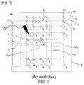
- the figure 1 represents a traditional image detector 10.
- the image detector 10 comprises a sensor 11 produced on a first monolithic substrate 12.
- the first monolithic substrate 12 comprises a set of pixels P(i,j) organized in a matrix 13 along rows Li and columns Cj.
- the matrix 13 can comprise any number of rows and columns thus forming pixels P(i,j).
- the matrix 13 forms a geographical area on the first substrate 12.
- the pixels are denoted in the generic form P(i,j), where i and j are natural integers designating respectively the rank of the row and the rank of the column in the matrix 13.
- the set of pixels P(i,j) is configured so as to generate signals as a function of radiation striking the detector 10.
- the sensor 11 comprises column conductors Yj, each connecting the pixels of the same column Cj.
- the column conductors Yj are intended to transport the signals generated by the pixels P(i,j).
- sensor 11 comprises line conductors Xi, each connecting the pixels of a same line Li.
- Matrix 13 of pixels P(i,j) comprises columns Cj of even ranks and odd ranks.
- the matrix 13 of pixels P(i,j) comprises rows Li of even ranks and of odd ranks.
- the sensor 10 comprises contact pads 14 located at the periphery of the first substrate 12 and outside the matrix 13 of pixels P(i,j). Contact pads 14 are connected to column conductors Yj.
- the image detector 10 comprises a row addressing block 15 located close to the first substrate 12 and connected to the row conductors Xi.
- a row addressing block 15 is any assembly comprising at least one row addressing block.
- the block 15 can be integrated into the first substrate 12, as represented on the figure 1 , or integrated into a separate substrate.
- the row addressing block 15 makes it possible to individually address each row of pixels Li.
- the image detector 10 comprises a column reading block 16 generally produced on a second substrate 17 different from the first substrate 12.
- the reading block of columns 16 comprises connection points 18 connecting the column read block 16 to the contact pads 14.
- the column read block 16 is used to read the signals generated by the pixels of the row selected by the row addressing block.
- a pixel P(i,j) comprises a photodiode Dp(i,j) associated with an electronic switch T(i,j).
- the photodiodes Dp(i,j) can of course be replaced by any photosensitive element capable of generating an electric signal when it is subjected to photon radiation.
- the pixel structure shown on the figure 1 is deliberately simplified and more complex structures can be implemented within the scope of the invention.
- the switch T(i,j) formed by a transistor is connected by its gate Gi to the line conductor Xi of line i, by its drain Dj to the column conductor Yj and by its source Sij to the cathode of the photodiode Dp (i,j).
- the anodes of all the photodiodes Dp(i,j) are connected to a common potential, for example ground.
- the row addressing block 15 includes elements making it possible to generate the signals to be injected onto the row conductors Xi to drive the opening and closing of the transistors T(i,j).
- the column read block 16 may include elements making it possible to process the signals received on the column conductors Yj. In particular, it may be an amplifier and/or an analog-to-digital converter.
- image sensor 11 operates as follows. During an image capture phase, the exposure of the photodiodes Dp(i,j) to radiation generates electrical charges at the source Sij. The quantity of charges at the level of each source Sij is a function of the intensity of the radiation received by the pixel P(i,j) considered. The image capture phase is followed by a reading phase carried out line by line. The signals injected into the various row conductors Xi pass successively to the active state, so that the potential of each column conductor Yj is successively representative of the quantity of electrical charges accumulated in the various pixels P(i,j) of column j.
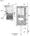
- the figure 2 schematically represents an image detector 10 of the prior art and the detail of a charge integration architecture of an image detector of the prior art.
- the digital detector 10 of the prior art comprises a plane sensor 11 produced on a first monolithic substrate.
- the flat collector 11 comprises a set of pixels P(i,j) organized in a matrix 13 along rows Li and columns Cj and configured so as to generate charges as a function of radiation 19 striking detector 10.
- Sensor 11 comprises conductors of columns Yj, each connecting the pixels P(i,j) of the same column Cj and intended to transport the charges generated by the pixels P(i,j). At this point, the signal is analog.
- At the output of sensor 11 there is a set of integrated reading circuits 33 with analog output.
- circuits 33 are connected to a daughter card 34, connected by card connectors 35 to analog/digital converters 31.
- the signal is analog-processed outside the first substrate.
- the analog signal area is represented by the reference SA.
- the digital processing, represented by the reference SN, takes place after the output of the analog/digital converters 31.
- each of the N columns is connected to an analog multiplexer 30, itself connected to an analog/digital converter block 31.
- the charges of the N channels that is to say N column conductors Yj, are integrated and sampled (29), then analog multiplexed to one or more analog/digital converter blocks 31 external.
- Data conversion is done outside the architecture and requires signal adaptation (gain, buffering 53, etc).
- a serializer block 23 makes it possible to serialize the signals to the output, for example to an FPGA circuit 36.
- a CDS correction is applied, that is to say that in the architecture of the prior art , there is a second reading with a prior reset of the column to make an empty reading of it which is then subtracted from the signal.
- the picture 3 schematically represents an image detector 100 according to the invention and the detail of a charge integration architecture of the image detector according to the invention.
- the basic description of the digital detector 100 is similar to that of the detector 10 of the figure 1 . The differences occur at the level of the integration block presented here in more detail on the right part of the figure. The references below, even if they are not all present on the picture 3 , are repeated based on the common elements with the detector of the figure 1 and some figure 2 for a better understanding.
- the digital detector 100 according to the invention comprises a flat sensor 11 and a first monolithic substrate and a second monolithic substrate, the flat sensor 11 being positioned on the first monolithic substrate.
- the plane sensor 11 comprises a set of pixels P(i,j) organized in a matrix 13 along rows Li and columns Cj and configured so as to generate charges as a function of radiation 19 striking the detector 100.
- the sensor 11 comprises column conductors Yj, each connecting the pixels P(i,j) of the same column Cj and intended to transport the charges generated by the pixels P(i,j).
- the detector comprises on the second monolithic substrate, distinct from the first substrate, for each of the column conductors Yj, a charge preamplifier 20 connected to the column conductor Yj, forming a preamplified column conductor 21j and intended to integrate the charges transported by said column conductor Yj.
- the sensor 11 comprises at least one analog/digital converter 22j connected in series to the preamplified column conductors 21j, intended to convert the charges integrated at the output of the charge preamplifiers 20 into a digital voltage.
- sensor 11 includes a serializer block 23 connected to at least one analog/digital converter 22j, intended to generate an output voltage from the digital voltages of at least one analog/digital converter 22j.
- the signal is analog-processed on the second monolithic substrate.
- the analog signal area is represented by the reference HER.
- the digital processing, represented by the reference SN takes place right from the output of the first monolithic substrate.
- the serializer block 23 is positioned on the second monolithic substrate, downstream of at least one analog/digital converter 22j.
- the analog/digital conversion is carried out on each channel in parallel before serialization on one or more digital outputs, this serialization being able to be likened to digital multiplexing.
- a particularity of the invention resides in the combination of the charge pre-amplifier and the analog/digital converter per channel upstream of the serializer block on a single monolithic substrate separated from the matrix of photodiodes.
- the principle of the invention is thus based on a monolithic circuit which ensures the conversion of charges into digital voltage.
- digitization takes place in each column, before multiplexing.
- the invention thus makes it possible to carry out a digital multiplexing that is less sensitive to noise and to disturbances of the analog signals.
- This digital multiplexing is made possible by the use of sigma-delta converters in each column.
- the invention aims to convert X-rays into charges via a specific sensor and then to amplify this charge (of the order of pC) to digitize it, by means of a preamplification stage and 'integration.
- the invention allows a conversion to more than 16 bits, on matrices typically of very large sizes (over a million pixels) for an equivalent number of frames.
- the invention proposes positioning the analog/digital converter on each channel and then carrying out digital multiplexing.
- the invention consists in performing a fusion, or imbrication, of the ADC on the second substrate. This results in a routing of the track with the rest of the blocks.
- the solution consists in associating, for each channel, a charge preamplifier 20 and an analog/digital converter (ADC) 22j in the same monolithic integrated circuit.
- ADC analog/digital converter
- this integration allows a significant improvement in the linearity, noise and crosstalk performances while reducing the cost and bulk of the components which carry out the integration/digitization function.
- each channel is associated with a charge preamplifier and an analog/digital converter (ADC) 22j is associated with several channels in the same monolithic integrated circuit.
- ADC analog/digital converter
- an analog/digital converter 22j is connected to several preamplified column conductors 21j. This variant shares the analog/digital converter between several channels in order to save surface area and reduce density when the application allows it.
- At least two of the preamplified column conductors 21j can be connected together and the at least two preamplified column conductors 21j connected together converge towards one of the at least one converter analogue/digital 22d.
- the invention is based on the production of a converter of electric charges originating from a matrix of pixels directly into a digital voltage on the second monolithic substrate. As seen on the figure 3 , at the output of the sensor, the signal is digital, the integrity of the data of this signal is thus ensured.
- the invention is distinguished from the prior art by the association, for each channel or at least for a plurality of channels, of a charge preamplifier and an analog/digital converter (ADC) in the same integrated circuit monolithic.
- ADC analog/digital converter
- the charge preamplifier overcomes the limitations of standard integration stages by allowing the charge to be integrated at the same rate as the transfer of the charge from the pixel via the column to the input of the integrator circuit.
- This arrangement has two advantages.
- the first advantage is the absence of loss of time: there is a significant gain in complete processing time and therefore in slab reading speed and transfer time (the data processing time is less than the integration time) .
- the second advantage is a significant reduction in the noise linked to the integration of the input load, in particular at high gain.
- the direct association of the preamplifier directly to the analog/digital converter ADC makes it possible to dispense with the traditional analog multiplexing stage between a group of columns and its single converter.
- the invention makes it possible to reduce the noise kTC induced by the column thanks to the specific assembly of the charge preamplifier nested with an analog-digital converter (ADC) in order to minimize the noise of the downstream chain.
- ADC analog-digital converter
- the invention makes it possible to meet the need which is to be able to integrate as quickly as possible the load coming from the matrix of pixels by generating the least possible disturbances of the signal (noise/linearity/leaks/crosstalk) which makes it possible to do the preamplifier load by associating it with an ADC within the same block on the same chip.
- the ADC and the transfer speed of the digital output must also be fast enough with regard to the characteristics of the matrix of pixels (time of convergence of the pixel in particular).
- the analog/digital converter is placed inside the column. There is no longer a multiplexer in this architecture, which saves time.
- the analog processing is carried out in the column and delivers a digital voltage at the column output.
- the notion of column is to be understood as being extended beyond the physical column on the photodiode array and including the individual "paths" in the conversion circuit external to the array. This eliminates signal stability or pollution issues.
- the detector of the invention allows digital signal processing, which ensures the integrity of the image of the analog data coming from the sensor.
- the particularity of the invention is based on the direct conversion of charges into a digital signal, without alteration of the signal by intermediate steps and/or stages.
- the invention is based on the coupling of the charge preamplifier with an analog/digital converter ADC in the same processing channel of a column of pixels.
- Associating the preamplifier with such a parallel ADC analog/digital converter thus makes it possible to create a real "charge-to-digital" converter (charge digitizer), the whole conversion being located in the processing channel of the column and not requiring no additional operations in analog form such as a multiplexing operation.
- the ADC analogue/digital converter must be parallel (i.e. we have one ADC analogue/digital converter per channel/preamplifier or alternatively per group of channels/preamplifiers) and integrated into the immediate processing chain of the column .
- the analog/digital converter ADC can be of any type (in particular successive approximations or sigma-delta), the resolution is irrelevant (generally 14 or 16 bits, or even more).
- the principle of the invention can be applied to all types of imagers with passive pixels (1T imager), in particular applications of the medical type, NDT.
Landscapes
- Engineering & Computer Science (AREA)
- Multimedia (AREA)
- Signal Processing (AREA)
- Health & Medical Sciences (AREA)
- Life Sciences & Earth Sciences (AREA)
- Physics & Mathematics (AREA)
- High Energy & Nuclear Physics (AREA)
- Molecular Biology (AREA)
- General Physics & Mathematics (AREA)
- Spectroscopy & Molecular Physics (AREA)
- Medical Informatics (AREA)
- Nuclear Medicine, Radiotherapy & Molecular Imaging (AREA)
- Surgery (AREA)
- Optics & Photonics (AREA)
- Pathology (AREA)
- Radiology & Medical Imaging (AREA)
- Biomedical Technology (AREA)
- Heart & Thoracic Surgery (AREA)
- Biophysics (AREA)
- Animal Behavior & Ethology (AREA)
- General Health & Medical Sciences (AREA)
- Public Health (AREA)
- Veterinary Medicine (AREA)
- Transforming Light Signals Into Electric Signals (AREA)
- Measurement Of Radiation (AREA)
- Solid State Image Pick-Up Elements (AREA)
Applications Claiming Priority (1)
| Application Number | Priority Date | Filing Date | Title |
|---|---|---|---|
| FR2101174A FR3119707A1 (fr) | 2021-02-08 | 2021-02-08 | Détecteur numérique à intégration numérique de charges |
Publications (1)
| Publication Number | Publication Date |
|---|---|
| EP4040780A1 true EP4040780A1 (de) | 2022-08-10 |
Family
ID=76730599
Family Applications (1)
| Application Number | Title | Priority Date | Filing Date |
|---|---|---|---|
| EP22155665.7A Pending EP4040780A1 (de) | 2021-02-08 | 2022-02-08 | Digitaler detektor mit digitaler ladungsintegration |
Country Status (5)
| Country | Link |
|---|---|
| US (1) | US20220256104A1 (de) |
| EP (1) | EP4040780A1 (de) |
| JP (1) | JP7842578B2 (de) |
| CN (1) | CN114910947A (de) |
| FR (1) | FR3119707A1 (de) |
Families Citing this family (1)
| Publication number | Priority date | Publication date | Assignee | Title |
|---|---|---|---|---|
| CN119404516A (zh) * | 2022-06-27 | 2025-02-07 | 索尼半导体解决方案公司 | 固态成像元件、成像装置和控制固态成像元件的方法 |
Citations (3)
| Publication number | Priority date | Publication date | Assignee | Title |
|---|---|---|---|---|
| US5184018A (en) | 1990-01-27 | 1993-02-02 | U.S. Philips Corporation | Sensor matrix |
| US6642494B1 (en) | 1998-07-31 | 2003-11-04 | Canon Kabushiki Kaisha | Photoelectric conversion apparatus, production method thereof, and information processing apparatus having the photoelectric conversion apparatus |
| US20200213543A1 (en) * | 2018-12-26 | 2020-07-02 | Canon Kabushiki Kaisha | Imaging apparatus and imaging system |
Family Cites Families (6)
| Publication number | Priority date | Publication date | Assignee | Title |
|---|---|---|---|---|
| JP3507800B2 (ja) * | 2001-02-02 | 2004-03-15 | 有限会社リニアセル・デザイン | アナログ−デジタル変換器及びこれを用いたイメージセンサ |
| JP2006075489A (ja) * | 2004-09-13 | 2006-03-23 | Hitachi Medical Corp | X線ct装置 |
| CA2835870A1 (en) * | 2011-05-12 | 2012-11-15 | Olive Medical Corporation | Pixel array area optimization using stacking scheme for hybrid image sensor with minimal vertical interconnects |
| US8817153B2 (en) | 2011-07-25 | 2014-08-26 | Aptina Imaging Corporation | Column parallel readout image sensors with shared column analog-to-digital converter circuitry |
| CN102752560B (zh) * | 2012-06-21 | 2014-11-12 | 吉林大学 | 基于像素电荷补偿技术的超宽动态范围图像传感器 |
| FR3013546B1 (fr) | 2013-11-15 | 2017-05-19 | Trixell | Mise en commun de deux colonnes de pixels d'un detecteur d'images |
-
2021
- 2021-02-08 FR FR2101174A patent/FR3119707A1/fr active Pending
-
2022
- 2022-02-07 CN CN202210115861.9A patent/CN114910947A/zh active Pending
- 2022-02-07 US US17/666,164 patent/US20220256104A1/en not_active Abandoned
- 2022-02-07 JP JP2022016907A patent/JP7842578B2/ja active Active
- 2022-02-08 EP EP22155665.7A patent/EP4040780A1/de active Pending
Patent Citations (3)
| Publication number | Priority date | Publication date | Assignee | Title |
|---|---|---|---|---|
| US5184018A (en) | 1990-01-27 | 1993-02-02 | U.S. Philips Corporation | Sensor matrix |
| US6642494B1 (en) | 1998-07-31 | 2003-11-04 | Canon Kabushiki Kaisha | Photoelectric conversion apparatus, production method thereof, and information processing apparatus having the photoelectric conversion apparatus |
| US20200213543A1 (en) * | 2018-12-26 | 2020-07-02 | Canon Kabushiki Kaisha | Imaging apparatus and imaging system |
Non-Patent Citations (2)
| Title |
|---|
| SIMONI A ET AL: "A digital vision sensor", 1 March 1995, SENSORS AND ACTUATORS A: PHYSICAL, ELSEVIER BV, NL, PAGE(S) 439 - 443, ISSN: 0924-4247, XP027220184 * |
| SIMONI ET AL., A DIGITAL VISION SENSOR |
Also Published As
| Publication number | Publication date |
|---|---|
| US20220256104A1 (en) | 2022-08-11 |
| FR3119707A1 (fr) | 2022-08-12 |
| CN114910947A (zh) | 2022-08-16 |
| JP7842578B2 (ja) | 2026-04-08 |
| JP2022121404A (ja) | 2022-08-19 |
Similar Documents
| Publication | Publication Date | Title |
|---|---|---|
| EP2398230B1 (de) | Linearer Bildsensor mit CMOS-Technologie | |
| US9343500B2 (en) | Solid-state imaging device, driving method thereof, and electronic device | |
| EP2564239B1 (de) | Detektor elektromagnetischer strahlung mit verstärkungsbereichauswahl | |
| EP2870631B1 (de) | Verfahren zur herstellung einer cmos-bildgebungsvorrichtung mit optimierter form mittels lichtsatz | |
| US20040051802A1 (en) | Differential readout from pixels in CMOS sensor | |
| EP3008756A1 (de) | Split-gate-bildsensor mit bedingter rücksetzung | |
| FR3039319A1 (fr) | Capteur d'image a pixels actifs avec fonctionnement en mode d'obturateur global, soustraction du bruit de reinitialisation et lecture non destructive | |
| EP2408194B1 (de) | Bilderfassungsgerät mit CMOS-Technologie mit einer starken Videofrequenz | |
| EP3629573B1 (de) | Schneller bilderfassungssensor mit pixel-binning | |
| FR2666714A1 (fr) | Detecteur d'image a pixels de grandes dimensions. | |
| EP2064868A1 (de) | Durch ladungstransfer arbeitender cmos-linearbildsensor | |
| TW201143412A (en) | Solid-state imaging device and method of reading signals from the pixel array of solid-state imaging device | |
| FR2867936A1 (fr) | Procede et capteur d'image pour effectuer un double sous-echantillonnage correle(cdss) de pixels dans une matrice de capteurs a pixels actifs (aps) | |
| EP4040780A1 (de) | Digitaler detektor mit digitaler ladungsintegration | |
| EP3900323B1 (de) | Pixelmatrix mit schneller pixel-binning | |
| EP2936800A1 (de) | Verfahren zum auslesen einer bildgebungsvorrichtung | |
| EP2486724B1 (de) | Verfahren zur rauschminderung im bildsignal eines bildsensors | |
| FR3131421A1 (fr) | Capteur d'images et procédé de commande d'un tel capteur | |
| FR2815502A1 (fr) | Dispositif de detection d'un flux photonique a balayage autoadaptatif | |
| FR2960096A1 (fr) | Capteur d'image lineaire en technologie cmos a contraintes temporelles relachees | |
| EP2664132A1 (de) | Linearer cmos-bildsensor mit bewegungsunschärfekompensation |
Legal Events
| Date | Code | Title | Description |
|---|---|---|---|
| PUAI | Public reference made under article 153(3) epc to a published international application that has entered the european phase |
Free format text: ORIGINAL CODE: 0009012 |
|
| STAA | Information on the status of an ep patent application or granted ep patent |
Free format text: STATUS: THE APPLICATION HAS BEEN PUBLISHED |
|
| AK | Designated contracting states |
Kind code of ref document: A1 Designated state(s): AL AT BE BG CH CY CZ DE DK EE ES FI FR GB GR HR HU IE IS IT LI LT LU LV MC MK MT NL NO PL PT RO RS SE SI SK SM TR |
|
| STAA | Information on the status of an ep patent application or granted ep patent |
Free format text: STATUS: REQUEST FOR EXAMINATION WAS MADE |
|
| 17P | Request for examination filed |
Effective date: 20230131 |
|
| RBV | Designated contracting states (corrected) |
Designated state(s): AL AT BE BG CH CY CZ DE DK EE ES FI FR GB GR HR HU IE IS IT LI LT LU LV MC MK MT NL NO PL PT RO RS SE SI SK SM TR |
|
| P01 | Opt-out of the competence of the unified patent court (upc) registered |
Effective date: 20230517 |