EP3603356B1 - Kontaktanordnung - Google Patents
Kontaktanordnung Download PDFInfo
- Publication number
- EP3603356B1 EP3603356B1 EP18711301.4A EP18711301A EP3603356B1 EP 3603356 B1 EP3603356 B1 EP 3603356B1 EP 18711301 A EP18711301 A EP 18711301A EP 3603356 B1 EP3603356 B1 EP 3603356B1
- Authority
- EP
- European Patent Office
- Prior art keywords
- contact
- arrangement
- connections
- circuit carrier
- access opening
- Prior art date
- Legal status (The legal status is an assumption and is not a legal conclusion. Google has not performed a legal analysis and makes no representation as to the accuracy of the status listed.)
- Active
Links
Images


Classifications
-
- H—ELECTRICITY
- H05—ELECTRIC TECHNIQUES NOT OTHERWISE PROVIDED FOR
- H05K—PRINTED CIRCUITS; CASINGS OR CONSTRUCTIONAL DETAILS OF ELECTRIC APPARATUS; MANUFACTURE OF ASSEMBLAGES OF ELECTRICAL COMPONENTS
- H05K3/00—Apparatus or processes for manufacturing printed circuits
- H05K3/30—Assembling printed circuits with electric components, e.g. with resistors
- H05K3/32—Assembling printed circuits with electric components, e.g. with resistors electrically connecting electric components or wires to printed circuits
- H05K3/34—Assembling printed circuits with electric components, e.g. with resistors electrically connecting electric components or wires to printed circuits by soldering
- H05K3/341—Surface mounted components
- H05K3/3431—Leadless components
- H05K3/3436—Leadless components having an array of bottom contacts, e.g. pad grid array or ball grid array components
-
- H—ELECTRICITY
- H05—ELECTRIC TECHNIQUES NOT OTHERWISE PROVIDED FOR
- H05K—PRINTED CIRCUITS; CASINGS OR CONSTRUCTIONAL DETAILS OF ELECTRIC APPARATUS; MANUFACTURE OF ASSEMBLAGES OF ELECTRICAL COMPONENTS
- H05K3/00—Apparatus or processes for manufacturing printed circuits
- H05K3/22—Secondary treatment of printed circuits
- H05K3/28—Applying non-metallic protective coatings
- H05K3/284—Applying non-metallic protective coatings for encapsulating mounted components
-
- H—ELECTRICITY
- H05—ELECTRIC TECHNIQUES NOT OTHERWISE PROVIDED FOR
- H05K—PRINTED CIRCUITS; CASINGS OR CONSTRUCTIONAL DETAILS OF ELECTRIC APPARATUS; MANUFACTURE OF ASSEMBLAGES OF ELECTRICAL COMPONENTS
- H05K2201/00—Indexing scheme relating to printed circuits covered by H05K1/00
- H05K2201/09—Shape and layout
- H05K2201/09009—Substrate related
- H05K2201/09072—Hole or recess under component or special relationship between hole and component
-
- H—ELECTRICITY
- H05—ELECTRIC TECHNIQUES NOT OTHERWISE PROVIDED FOR
- H05K—PRINTED CIRCUITS; CASINGS OR CONSTRUCTIONAL DETAILS OF ELECTRIC APPARATUS; MANUFACTURE OF ASSEMBLAGES OF ELECTRICAL COMPONENTS
- H05K2201/00—Indexing scheme relating to printed circuits covered by H05K1/00
- H05K2201/09—Shape and layout
- H05K2201/09209—Shape and layout details of conductors
- H05K2201/09654—Shape and layout details of conductors covering at least two types of conductors provided for in H05K2201/09218 - H05K2201/095
- H05K2201/09781—Dummy conductors, i.e. not used for normal transport of current; Dummy electrodes of components
-
- H—ELECTRICITY
- H05—ELECTRIC TECHNIQUES NOT OTHERWISE PROVIDED FOR
- H05K—PRINTED CIRCUITS; CASINGS OR CONSTRUCTIONAL DETAILS OF ELECTRIC APPARATUS; MANUFACTURE OF ASSEMBLAGES OF ELECTRICAL COMPONENTS
- H05K2201/00—Indexing scheme relating to printed circuits covered by H05K1/00
- H05K2201/10—Details of components or other objects attached to or integrated in a printed circuit board
- H05K2201/10613—Details of electrical connections of non-printed components, e.g. special leads
- H05K2201/10621—Components characterised by their electrical contacts
- H05K2201/10674—Flip chip
-
- H—ELECTRICITY
- H05—ELECTRIC TECHNIQUES NOT OTHERWISE PROVIDED FOR
- H05K—PRINTED CIRCUITS; CASINGS OR CONSTRUCTIONAL DETAILS OF ELECTRIC APPARATUS; MANUFACTURE OF ASSEMBLAGES OF ELECTRICAL COMPONENTS
- H05K2201/00—Indexing scheme relating to printed circuits covered by H05K1/00
- H05K2201/10—Details of components or other objects attached to or integrated in a printed circuit board
- H05K2201/10613—Details of electrical connections of non-printed components, e.g. special leads
- H05K2201/10621—Components characterised by their electrical contacts
- H05K2201/10704—Pin grid array [PGA]
-
- H—ELECTRICITY
- H05—ELECTRIC TECHNIQUES NOT OTHERWISE PROVIDED FOR
- H05K—PRINTED CIRCUITS; CASINGS OR CONSTRUCTIONAL DETAILS OF ELECTRIC APPARATUS; MANUFACTURE OF ASSEMBLAGES OF ELECTRICAL COMPONENTS
- H05K2201/00—Indexing scheme relating to printed circuits covered by H05K1/00
- H05K2201/10—Details of components or other objects attached to or integrated in a printed circuit board
- H05K2201/10613—Details of electrical connections of non-printed components, e.g. special leads
- H05K2201/10621—Components characterised by their electrical contacts
- H05K2201/10719—Land grid array [LGA]
-
- H—ELECTRICITY
- H05—ELECTRIC TECHNIQUES NOT OTHERWISE PROVIDED FOR
- H05K—PRINTED CIRCUITS; CASINGS OR CONSTRUCTIONAL DETAILS OF ELECTRIC APPARATUS; MANUFACTURE OF ASSEMBLAGES OF ELECTRICAL COMPONENTS
- H05K2201/00—Indexing scheme relating to printed circuits covered by H05K1/00
- H05K2201/10—Details of components or other objects attached to or integrated in a printed circuit board
- H05K2201/10613—Details of electrical connections of non-printed components, e.g. special leads
- H05K2201/10621—Components characterised by their electrical contacts
- H05K2201/10734—Ball grid array [BGA]; Bump grid array
-
- H—ELECTRICITY
- H05—ELECTRIC TECHNIQUES NOT OTHERWISE PROVIDED FOR
- H05K—PRINTED CIRCUITS; CASINGS OR CONSTRUCTIONAL DETAILS OF ELECTRIC APPARATUS; MANUFACTURE OF ASSEMBLAGES OF ELECTRICAL COMPONENTS
- H05K2201/00—Indexing scheme relating to printed circuits covered by H05K1/00
- H05K2201/10—Details of components or other objects attached to or integrated in a printed circuit board
- H05K2201/10613—Details of electrical connections of non-printed components, e.g. special leads
- H05K2201/10954—Other details of electrical connections
- H05K2201/10977—Encapsulated connections
-
- H—ELECTRICITY
- H05—ELECTRIC TECHNIQUES NOT OTHERWISE PROVIDED FOR
- H05K—PRINTED CIRCUITS; CASINGS OR CONSTRUCTIONAL DETAILS OF ELECTRIC APPARATUS; MANUFACTURE OF ASSEMBLAGES OF ELECTRICAL COMPONENTS
- H05K2203/00—Indexing scheme relating to apparatus or processes for manufacturing printed circuits covered by H05K3/00
- H05K2203/08—Treatments involving gases
- H05K2203/085—Using vacuum or low pressure
-
- H—ELECTRICITY
- H05—ELECTRIC TECHNIQUES NOT OTHERWISE PROVIDED FOR
- H05K—PRINTED CIRCUITS; CASINGS OR CONSTRUCTIONAL DETAILS OF ELECTRIC APPARATUS; MANUFACTURE OF ASSEMBLAGES OF ELECTRICAL COMPONENTS
- H05K2203/00—Indexing scheme relating to apparatus or processes for manufacturing printed circuits covered by H05K3/00
- H05K2203/11—Treatments characterised by their effect, e.g. heating, cooling, roughening
- H05K2203/1178—Means for venting or for letting gases escape
-
- H—ELECTRICITY
- H10—SEMICONDUCTOR DEVICES; ELECTRIC SOLID-STATE DEVICES NOT OTHERWISE PROVIDED FOR
- H10W—GENERIC PACKAGES, INTERCONNECTIONS, CONNECTORS OR OTHER CONSTRUCTIONAL DETAILS OF DEVICES COVERED BY CLASS H10
- H10W70/00—Package substrates; Interposers; Redistribution layers [RDL]
- H10W70/60—Insulating or insulated package substrates; Interposers; Redistribution layers
- H10W70/67—Insulating or insulated package substrates; Interposers; Redistribution layers characterised by their insulating layers or insulating parts
- H10W70/68—Shapes or dispositions thereof
- H10W70/681—Shapes or dispositions thereof comprising holes not having chips therein, e.g. for outgassing, underfilling or bond wire passage
-
- H—ELECTRICITY
- H10—SEMICONDUCTOR DEVICES; ELECTRIC SOLID-STATE DEVICES NOT OTHERWISE PROVIDED FOR
- H10W—GENERIC PACKAGES, INTERCONNECTIONS, CONNECTORS OR OTHER CONSTRUCTIONAL DETAILS OF DEVICES COVERED BY CLASS H10
- H10W72/00—Interconnections or connectors in packages
- H10W72/071—Connecting or disconnecting
- H10W72/072—Connecting or disconnecting of bump connectors
-
- H—ELECTRICITY
- H10—SEMICONDUCTOR DEVICES; ELECTRIC SOLID-STATE DEVICES NOT OTHERWISE PROVIDED FOR
- H10W—GENERIC PACKAGES, INTERCONNECTIONS, CONNECTORS OR OTHER CONSTRUCTIONAL DETAILS OF DEVICES COVERED BY CLASS H10
- H10W72/00—Interconnections or connectors in packages
- H10W72/071—Connecting or disconnecting
- H10W72/073—Connecting or disconnecting of die-attach connectors
-
- H—ELECTRICITY
- H10—SEMICONDUCTOR DEVICES; ELECTRIC SOLID-STATE DEVICES NOT OTHERWISE PROVIDED FOR
- H10W—GENERIC PACKAGES, INTERCONNECTIONS, CONNECTORS OR OTHER CONSTRUCTIONAL DETAILS OF DEVICES COVERED BY CLASS H10
- H10W74/00—Encapsulations, e.g. protective coatings
- H10W74/01—Manufacture or treatment
- H10W74/012—Manufacture or treatment of encapsulations on active surfaces of flip-chip devices, e.g. forming underfills
-
- H—ELECTRICITY
- H10—SEMICONDUCTOR DEVICES; ELECTRIC SOLID-STATE DEVICES NOT OTHERWISE PROVIDED FOR
- H10W—GENERIC PACKAGES, INTERCONNECTIONS, CONNECTORS OR OTHER CONSTRUCTIONAL DETAILS OF DEVICES COVERED BY CLASS H10
- H10W74/00—Encapsulations, e.g. protective coatings
- H10W74/10—Encapsulations, e.g. protective coatings characterised by their shape or disposition
- H10W74/15—Encapsulations, e.g. protective coatings characterised by their shape or disposition on active surfaces of flip-chip devices, e.g. underfills
-
- H—ELECTRICITY
- H10—SEMICONDUCTOR DEVICES; ELECTRIC SOLID-STATE DEVICES NOT OTHERWISE PROVIDED FOR
- H10W—GENERIC PACKAGES, INTERCONNECTIONS, CONNECTORS OR OTHER CONSTRUCTIONAL DETAILS OF DEVICES COVERED BY CLASS H10
- H10W90/00—Package configurations
- H10W90/701—Package configurations characterised by the relative positions of pads or connectors relative to package parts
- H10W90/721—Package configurations characterised by the relative positions of pads or connectors relative to package parts of bump connectors
- H10W90/724—Package configurations characterised by the relative positions of pads or connectors relative to package parts of bump connectors between a chip and a stacked insulating package substrate, interposer or RDL
-
- H—ELECTRICITY
- H10—SEMICONDUCTOR DEVICES; ELECTRIC SOLID-STATE DEVICES NOT OTHERWISE PROVIDED FOR
- H10W—GENERIC PACKAGES, INTERCONNECTIONS, CONNECTORS OR OTHER CONSTRUCTIONAL DETAILS OF DEVICES COVERED BY CLASS H10
- H10W90/00—Package configurations
- H10W90/701—Package configurations characterised by the relative positions of pads or connectors relative to package parts
- H10W90/731—Package configurations characterised by the relative positions of pads or connectors relative to package parts of die-attach connectors
- H10W90/734—Package configurations characterised by the relative positions of pads or connectors relative to package parts of die-attach connectors between a chip and a stacked insulating package substrate, interposer or RDL
-
- Y—GENERAL TAGGING OF NEW TECHNOLOGICAL DEVELOPMENTS; GENERAL TAGGING OF CROSS-SECTIONAL TECHNOLOGIES SPANNING OVER SEVERAL SECTIONS OF THE IPC; TECHNICAL SUBJECTS COVERED BY FORMER USPC CROSS-REFERENCE ART COLLECTIONS [XRACs] AND DIGESTS
- Y02—TECHNOLOGIES OR APPLICATIONS FOR MITIGATION OR ADAPTATION AGAINST CLIMATE CHANGE
- Y02P—CLIMATE CHANGE MITIGATION TECHNOLOGIES IN THE PRODUCTION OR PROCESSING OF GOODS
- Y02P70/00—Climate change mitigation technologies in the production process for final industrial or consumer products
- Y02P70/50—Manufacturing or production processes characterised by the final manufactured product
Definitions
- the invention relates to a contact arrangement comprising a circuit carrier according to the preamble of the independent claim.
- underfill is often used to increase the reliability of electronic assemblies.
- This corresponds to a filler material which, after an electronic component has been fitted onto a circuit carrier, is introduced into an existing spacing gap between the electronic component and the circuit carrier and completely fills it.
- a main load caused by predominantly mechanical shock can be counteracted.
- thermal shock loads there is an optimization for thermal shock loads.
- underfill processes use capillary forces to suck the underfill, which is dispensed laterally along the edge of the component, under the component.
- An alternative form of underfilling is to apply the material under pressure through a hole in the circuit board between external contact connections of the electronic component, as is the case, for example, in the explanations of the patent US5766982 is shown. This method has various advantages, but can only be used if it is possible to form an access opening for the underfill between electrically contacted contact connections of the electronic component, for example by drilling.
- a contact arrangement comprising a circuit carrier and an electronic component contacted with the circuit carrier is known.
- an opening in the circuit carrier below the contacted electronic component is used to facilitate the suction of an underfill into the gap between the circuit carrier and the electronic component by attaching a vacuum device and to ensure that it is completely filled.
- the opening is formed between two rows with contact connections which are each arranged in the edge region of the electronic component.
- US2015 / 0262956 A shows a contact arrangement between a semiconductor component and a substrate carrier, the substrate carrier having a continuous opening across the substrate thickness cross-section in a connection region with the semiconductor component.
- the invention is based on the object of ensuring the introduction of an underfill or a filler material into a gap between a circuit carrier and an electronic component electrically contacted with the circuit carrier, in particular in the case of electronic components with a small pitch dimension.
- the starting point is a contact arrangement comprising a circuit carrier with an upper and a lower side and at least one electronic component, the circuit carrier having at least contact points on the upper side which are electrically contacted with contact terminals of the electronic component.
- it comprises a filler material which fills a gap between the top of the circuit carrier and the electronic component, the circuit carrier having an access opening for introducing the filler material.
- the filler material can be injected from the underside of the circuit carrier, for example under pressure, or it can be sucked in from the upper side of the circuit carrier by means of negative pressure.
- the electronic component has a pattern arrangement of the contact connections on a component side facing the upper side of the circuit carrier, with a connection surface being at least partially covered by exactly one of three closest adjacent contact connections in a perpendicular projection onto the upper side of the access opening. Furthermore, the contact connection associated with the covered connection surface is free from electrical contacting. This advantageously results in the possibility of feeding the filler material past the associated contact connection through the access opening and of enabling the said spacing gap to be filled. Despite the proximity of the contact connection to the access opening and the resulting type of shading or mechanical hurdle, flow of the filler material is hardly hindered, especially if a gap remains between the associated contact connection and the opening and / or the circuit carrier.
- connection contact present as being free of electrical contacting is preferably selected from a group of redundant contact connections of the electronic component, in particular a ground connection or a voltage supply connection. In this way, the electrical functions of the electronic component can still be fully used. In addition, an electrical function of the entire electronic component is not endangered by purely mechanical damage to the associated contact connection mentioned. Overall, the use of electronic components is now advantageously made possible, which have contact connections that are very close to one another and which were previously excluded from the safe introduction of a filler material in the manner already described. If necessary, connection surfaces of more than one of the next adjacent contact connections can also be used in the same way be at least partially covered. However, this reduces the number of remaining electrically contactable contact connections, so that preferably only one contact connection is sacrificed in the manner described for an access opening.
- connection contact arrangement results when the covered connection surface in the projection is arranged completely within the access opening.
- connection contact is preferably centered from the top above the access opening, with an essentially equal gap remaining on all sides in relation to the access opening. In this way, a very uniform and symmetrical flow of the filling material between the top and the component side of the electronic component is made possible, so that a filling capacity is very beneficial.
- An embodiment of the contact arrangement is preferred in which the three closest adjacent contact connections are arranged in a line and the contact connection associated with the covered connection surface forms the middle contact connection. Accordingly, the two outer contact connections are electrically contacted with contact points of the circuit carrier and the middle contact connection is sacrificed to enable the filling material to be introduced while its electrical function is omitted.
- the previous requirement of a sufficient distance between two directly adjacent contact connections in relation to the size of an access opening to be provided can thus advantageously be extended to the distance between the two outer contact connections in the row of lines.
- the pattern arrangement of the contact connections is formed as an arrangement of the contact connections in a grid of parallel rows and parallel columns.
- the row and / or column spacings are preferably constant, and the row and column spacings are more preferably the same.
- the pattern arrangement is designed in particular in such a way that the rows and columns intersect perpendicularly and the contact connections are arranged at the respective intersection points. The same applies to an embodiment in which the rows and columns intersect at an angle other than 90 °, creating an arrangement, for example is in the form of a honeycomb lattice.
- designs are conceivable in which no electrical contact connection is formed in individual of the above-mentioned intersections, preferably only a minority thereof. Overall, a large number of standard components can be used in this way or electronic components which have a connection diagram based on the standard components.
- a pitch distance is preferably present from the two closest adjacent contact connections.
- the pitch distance is shown as a center-center distance between two nearest adjacent contact connections.
- points or axes of symmetry of the respective contact connections are used and their smallest spacing from one another is determined.
- a very simple determination results from an overall symmetrical pattern arrangement of the contact connections. So-called pitch specifications are well known in electronics manufacturing.
- All contact connections of the pattern arrangement preferably have the same pitch spacing from one another.
- the clear width accordingly characterizes the largest opening dimension of the access opening.
- the maximum clear width is preferably obtained between two edge points of the access opening, of which at least one edge point, preferably both, has a shortest distance to a respectively closest electrically contacted contact connection.
- the filler material can be introduced into the spacing gap between the electronic component and the circuit carrier, in particular under pressure, for example by injection.
- the opening diameter preferably has at least that double the size of the spacing gap, which means that the filling material can also be drawn in due to capillary forces.
- the component side having the pattern arrangement of the contact connections in the projection has a centroid in the projected area, with at least one access opening formed in the circuit carrier being arranged in the area of the centroid.
- the projected area is preferably a circular area. Square or rectangular, oval, diamond-shaped or generally symmetrical polygonal surface shapes are also conceivable, for example a pentagon, hexagon and others.
- the center of gravity can be determined according to known geometric rules. As a rule, the projected area corresponds to a correspondingly flat component side.
- Such a formed access opening is accordingly arranged in a central region below the component side having the pattern arrangement of the contact connections.
- the spacing gap is filled from several points at the same time, which means that short cycle times can be maintained in series production.
- the two or more access openings which are arranged point-symmetrically and / or rotationally symmetrically, are arranged to one another in such a way that concentric circles of the same size touch each other at one point around their respective opening axis, a sum of the circular areas formed at least 60% and max 140% of the projected area corresponds to the component side.
- a respective distance between the access opening and the center of gravity is set that a respective flow front of the filling material spreading concentrically around an access opening simultaneously reaches a respective outer component edge and fills the complete spacing gap between the electronic component and the circuit carrier in each area is. Filling can therefore take place in the shortest possible time.
- BGA ball grid array
- LGA latitude and low-latency
- PGA pin grid array
- WLP wafer level packaging
- Exemplary designs for a BGA component are: FBGA (Fine Pitch Ball Grid Array), LBGA (Low Profile Ball Grid Array), TEPBGA (Thermally Enhanced Plastic Ball Grid Array), CBGA (Ceramic Ball Grid Array), OBGA (Organic Ball Grid Array), TFBGA (Thin Fine Pitch Ball Grid Array), PBGA (Plastic Ball Grid Array), MAP-BGA (Mold Array Process - Ball Grid Array), UCSP Micro (( ⁇ ) Chip Scale Package), ⁇ BGA (Micro-Ball Grid Array), LFBGA (Low Profile Fine Pitch Ball Grid Array), TBGA (Thin Ball Grid Array), SBGA (Super Ball Grid Array), UFBGA (Ultra Fine Ball Grid Array), FC-B
- Exemplary designs for a PGA component are: OPGA (Organic Pin Grid Array), FCPGA (Flip-chip Pin Grid Array), PAC (Pin Array Cartridge), PGA (Pin grid array), CPGA (Ceramic Pin Grid Array).
- OPGA Organic Pin Grid Array
- FCPGA Flexible Pin Grid Array
- PAC Pin-chip Pin Grid Array
- PGA Pin grid array
- CPGA Ceramic Pin Grid Array
- a first embodiment of a contact arrangement 100 is shown in a lateral sectional view.
- the contact arrangement 100 here comprises at least one circuit carrier 10, which has an upper side 11 and an underside 12.
- At least one electrical component 20 is electrically contacted with the circuit carrier 10.
- the top 11 has a plurality of contact points (also referred to as pads, not shown), which are electrically connected to complementary contact connections 25 of the electrical component 20, for example by means of a solder material.
- the contact connections 25 are arranged in a pattern arrangement on a component element side 22 facing the top side 11. In the sectional view of the Fig. 1 only a number of contact connections 25 are shown, which are arranged in a line. Possible pattern arrangements will be made later with the help of the Figures 2a-2d explained.
- the circuit carrier 10 has an access opening 15 which penetrates the upper side 11 and the lower side 12.
- the access opening 15 enables a filler material 30 to be introduced into a spacing gap 13 formed between the electronic component 20 and the circuit carrier 10. This can be done, for example, by a filling device 40 which injects the filling material 30 with pressure through the access opening 15. As the degree of filling increases, the spacing gap 13 is then preferably completely filled with the filling material 30 up to the component edges (shown in dashed lines).
- the access opening 15 is such in the circuit carrier 10 and in relation to the Pattern arrangement arranged on contact connections 25 that at least one contact connection 25 'is at least partially free-standing above the access opening 15, in particular centered on this, and is thus free of any electrical contact.
- FIG Fig. 2a The arrangement of the access opening is further illustrated in FIG Fig. 2a shown.
- a vertical view A of the upper side 11 of the circuit carrier 10 this shows only the projection surface 22 'of the component side 22 identified above and the projection surfaces of the arranged contact connections 25 resulting from a pattern arrangement.
- a border of the circuit carrier 10 is also shown in dashed lines.
- the pattern arrangement of the contact connections 25 is formed, for example, as an arrangement of the contact connections 25 in a grid of parallel rows and parallel columns, in particular in the form of an nx m matrix, where n denotes the number of columns and m denotes the number of rows .
- grid lines are shown, with the contact connections 25 preferably at all intersections of the grid lines are trained.
- a pattern arrangement can also be designed in other shapes.
- the contact connections 25 arranged in line in a column n have a pitch spacing pm and the contact connections 25 arranged in a row m have a pitch distance pn.
- the edge of the access opening 15 can also be seen, which, for example, encloses a circular area due to a cylindrical design of the access opening 15. It can be seen that in the projection in a group of adjacent contact connections 25, the connection area of at least one of the three closest contact connections 25 within the Edge of the access opening 15 is arranged. Accordingly, the relevant connection surface of the one contact connection 25 ′ is completely covered by the surface of the access opening 15 in the projection. Alternatively, there can also be only a partial overlap and / or the connection surfaces of a plurality of contact connections 25 ′ can be completely or partially covered in this way.
- the access opening 15 is preferably in or at least in a direct area of the centroid S of the projection surface 22 'of the component side 22 is arranged. This results in a very central access to the filling material 30 for filling the spacing gap 13.
- the second embodiment of the contact arrangement according to FIG Figure 2b has a total of 3 access openings 15 in the circuit carrier 10. These are arranged rotationally symmetrically around the center of gravity S at 120 ° angular distances from one another. These access openings 15 are preferably arranged at a respective distance from the centroid S in such a way that concentric circles of the same size touch each other at one point around their respective opening axis (shown in dashed lines), with a sum of the circular areas formed at least 60% and at most 140 % of the projected area 22 ′ of the component side 22 correspond.
- a fourth access opening can also be arranged in the center of gravity S (shown in dashed lines). In contrast to the execution for Fig. 2a a larger number of contact connections 25 is shown.
- the third embodiment of the contact arrangement is in Figure 2c shown.
- this shows a total of two access openings 15, which are arranged diagonally opposite in alignment with the corners of the projection surface 22 'of the component side 22, in particular point and / or rotationally symmetrical to the center of gravity S.
- a total of three access openings 15 are arranged in alignment with the corners of the projection surface 22 'of the component side 22, in part similar to the third embodiment.
- an electrical Component 20 can alternatively or additionally be arranged in an electrically contacted manner on the underside 12 of the circuit carrier 10.
- the contacted components 20 of various designs of the contact arrangement 100 preferably have a housing shape in accordance with an embodiment of BGA (ball grid array), LGA (land grid array), PGA (pin grid array) or WLP (wafer level packaging).
- BGA ball grid array
- LGA laand grid array
- PGA pin grid array
- WLP wafer level packaging
Landscapes
- Engineering & Computer Science (AREA)
- Manufacturing & Machinery (AREA)
- Microelectronics & Electronic Packaging (AREA)
- Wire Bonding (AREA)
- Structures Or Materials For Encapsulating Or Coating Semiconductor Devices Or Solid State Devices (AREA)
Description
- Die Erfindung betrifft eine Kontaktanordnung, umfassend einen Schaltungsträger, gemäß dem Oberbegriff des unabhängigen Anspruches.
- Zur Steigerung der Zuverlässigkeit elektronischer Baugruppen wird oft ein sogenannter Underfill verwendet. Dies entspricht einem Füllmaterial, welches in der Regel nach dem Bestücken eines elektronischen Bauelementes auf einem Schaltungsträger in einen vorliegenden Abstandsspalt zwischen dem elektronischen Bauelement und dem Schaltungsträger eingebracht wird und diesen vollständig ausfüllt. Im Consumer-Bereich kann dadurch beispielsweise einer Hauptbelastung durch überwiegend mechanischen Schock entgegengewirkt werden. Im Automobilbereich erfolgt eine Optimierung auf eine Temperaturwechsel-Belastung hin.
- Gängige Underfill-Prozesse nutzen Kapillarkräfte, um den seitlich entlang der Bauelementkante dispensten Underfill unter das Bauelement zu saugen. Eine alternative Form des Unterfüllens ist das Material unter Druck durch ein Loch in der Leiterplatte zwischen außenliegenden Kontaktanschlüssen des elektronischen Bauelements zu applizieren, wie das beispielsweise in Ausführungen der Patentschrift
US5766982 gezeigt ist. Dieses Verfahren hat diverse Vorteile, ist aber nur anwendbar, wenn es möglich ist, zwischen elektrisch kontaktierten Kontaktanschlüssen des elektronischen Bauelements eine Zugangsöffnung für den Underfill, beispielsweise durch Bohren, auszubilden. - Besonders elektronische Bauelemente, beispielsweise ein BGA-Bauelement (ball grid array), mit sehr kleinem Mitten-Mitten-Abstand der Kontaktanschlüsse (Pitch) benötigen oft einen Underfill. Leider ist es gerade bei diesen Bauelementen oft nicht möglich, aufgrund eines sehr kleinen Pitches, Öffnungen zwischen den angeordneten Kontaktanschlüssen vorzusehen. Dadurch ist die Zuverlässigkeit des elektronischen Bauelements gefährdet.
- Aus der Offenlegungsschrift
US2009/0229513 ist eine Kontaktanordnung, umfassend einen Schaltungsträger und ein mit dem Schaltungsträger kontaktiertes elektronisches Bauelement, bekannt. Hierbei wird eine Öffnung in dem Schaltungsträger unterhalb des kontaktierten elektronischen Bauelements dazu genutzt, durch Ansetzen einer Unterdruckvorrichtung das Ansaugen eines Underfills in den Abstandsspalt zwischen dem Schaltungsträger und dem elektronischen Bauelement zu erleichtern und ein vollständiges Ausfüllen sicherzustellen. Die Öffnung ist dabei zwischen zwei jeweils im Randbereich des elektronischen Bauelementes angeordneten Reihen mit Kontaktanschlüssen ausgebildet. - Die Patentschrift
US4644445 zeigt eine artähnliche Kontaktanordnung, wobei allerdings Leiterbahnstrukturen des Schaltungsträgers über eine Öffnung im Schaltungsträger geführt sind zur elektrischen Kontaktierung von Kontaktanschlüssen eines elektronischen Bauelements. Ein Underfill kann seitlich an dem die Öffnung überbrückenden Teilabschnitt der Leiterbahnstruktur vorbei in den Abstandsspalt eingebracht werden. Das Einbringen des Underfills birgt jedoch die Gefahr, die Leiterbahnstruktur zu beschädigen und dadurch die eigentliche elektrische Funktion schädlich zu unterbinden. - Die Offenlegungsschrift
US2015/0262956 A zeigt eine Kontaktanordnung zwischen einen Halbleiterbauelement und einem Substratträger, wobei der Substratträger in einem Verbindungbereich mit dem Halbleiterbauelement eine durchgehende Öffnung über den Substratdickenquerschnitt hinweg aufweist. - Der Erfindung liegt die Aufgabe zu Grunde, das Einbringen eines Underfills bzw. eines Füllmaterials in einen Abstandsspalt zwischen einem Schaltungsträger und einem mit dem Schaltungsträger elektrisch kontaktierten elektronischen Bauelement sicherzustellen, insbesondere bei elektronischen Bauelementen mit einem kleinen Pitchabstandsmaß.
- Diese Aufgabe wird durch eine Kontaktanordnung mit den kennzeichnenden Merkmalen des unabhängigen Anspruches gelöst.
- Ausgegangen wird von einer Kontaktanordnung, umfassend einen Schaltungsträger mit einer Ober- und einer Unterseite und zumindest ein elektronisches Bauelement, wobei der Schaltungsträger zumindest Kontaktstellen auf der Oberseite aufweist, die mit Kontaktanschlüssen des elektronischen Bauelements elektrisch kontaktiert sind. Zusätzlich umfasst es ein Füllmaterial, welches einen Abstandsspalt zwischen der Oberseite des Schaltungsträgers und dem elektronischen Bauelement ausfüllt, wobei der Schaltungsträger eine Zugangsöffnung zum Einbringen des Füllmaterials aufweist. Hierbei kann das Füllmaterial von der Unterseite des Schaltungsträgers her beispielsweise unter Druck eingespritzt werden oder mittels Unterdruck von der Oberseite des Schaltungsträgers angesaugt werden. Das elektronische Bauelement weist auf einer der Oberseite des Schaltungsträgers zugewandten Bauelementenseite eine Musteranordnung der Kontaktanschlüssen auf, wobei eine Anschlussfläche von genau einem von drei nächst benachbarten Kontaktanschlüssen in einer senkrechten Projektion auf die Oberseite von der Zugangsöffnung zumindest teilweise überdeckt ist. Ferner ist der zur überdeckten Anschlussfläche zugehörige Kontaktanschluss frei von einer elektrischen Kontaktierung. In vorteilhafter Weise ergibt sich dadurch die Möglichkeit, das Füllmaterial durch die Zugangsöffnung an dem zugehörigen Kontaktanschluss vorbeizuführen und ein Befüllen des genannten Abstandsspaltes zu ermöglichen. Trotz einer Nähe des Kontaktanschlusses zur Zugangsöffnung und einer dadurch vorliegenden Art von Beschattung bzw. mechanischen Hürde, ist ein Durchfluss des Füllmaterials kaum behindert, insbesondere, wenn zwischen dem zugehörigen Kontaktanschluss und der Öffnung und/oder dem Schaltungsträger ein Spaltabstand verbleibt. Bevorzugt ist der als frei von einer elektrischen Kontaktierung vorliegende Anschlusskontakt gewählt aus einer Gruppe von redundanten Kontaktanschlüssen des elektronischen Bauelements, insbesondere ein Masseanschluss oder ein Spannungsversorgungsanschluss. Auf diese Weise sind die elektrischen Funktionen des elektronischen Bauelements weiterhin voll nutzbar. Zusätzlich ist eine elektrische Funktion des gesamten elektronischen Bauelements durch eine rein mechanische Beschädigung des genannten zugehörigen Kontaktanschlusses nicht gefährdet. Insgesamt ist auch der Einsatz von elektronischen Bauelementen nun vorteilhaft ermöglicht, die sehr nah zueinander liegende Kontaktanschlüsse aufweisen und welche bisher von einem sicheren Einbringen eines Füllmaterials in bereits beschriebener Weise ausgeschlossen waren. Falls erforderlich, können auch Anschlussflächen von mehr als einem der nächst benachbarten Kontaktanschlüssen in gleicher Weise zumindest teilweise überdeckt sein. Allerdings reduziert sich dadurch die Anzahl verbleibender elektrisch kontaktierbarer Kontaktanschlüsse, so dass bevorzugt ausschließlich nur ein Kontaktanschluss in beschriebener Weise für eine Zugangsöffnung geopfert wird.
- Eine besonders günstige Ausführungsform der Kontaktanordnung ergibt sich, wenn die überdeckte Anschlussfläche in der Projektion vollständig innerhalb der Zugangsöffnung angeordnet ist. In einem gedachten Seitenschnitt durch die Zugangsöffnung hindurch steht der Anschlusskontakt von der Oberseite her bevorzugt zentriert oberhalb der Zugangsöffnung, wobei allseitig in Bezug zur Zugangsöffnung ein im Wesentlichen gleicher Spalt verbleibt. Auf diese Weise ist ein sehr gleichmäßiger und symmetrischer Fluss des Füllmaterials zwischen der Oberseite und der Bauelementenseite des elektronischen Bauelements ermöglicht, so dass ein Füllvermögen sehr begünstigt ist.
- Bevorzugt ist eine Ausführungsform der Kontaktanordnung, bei welcher die drei nächst benachbarten Kontaktanschlüsse in einer Linie angeordnet sind und der zur überdeckten Anschlussfläche zugehörige Kontaktanschluss den mittleren Kontaktanschluss bildet. Demnach sind die äußeren beiden Kontaktanschlüsse elektrisch mit Kontaktstellen des Schaltungsträgers kontaktiert und der mittlere Kontaktanschluss zum Ermöglichen eines Einbringens des Füllmaterials unter Wegfall von dessen elektrischer Funktion geopfert. Die bisherige Forderung eines ausreichenden Abstandes von zwei unmittelbar benachbarten Kontaktanschlüssen in Bezug auf eine Größe einer vorzusehenden Zugangsöffnung kann damit vorteilhaft auf den Abstand der äußeren beiden Kontaktanschlüsse in der Linienreihe erweitert werden.
- In einer Weiterbildung der Kontaktanordnung ist die Musteranordnung der Kontaktanschlüsse gebildet als eine Anordnung der Kontaktanschlüsse in einem Raster von parallelen Zeilen und parallelen Spalten. Bevorzugt sind die Zeilen- und/oder Spaltenabstände zueinander gleichbleibend, weiter bevorzugt entsprechen sich die Zeilen- und Spaltenabstände. Die Musteranordnung ist insbesondere derart ausgebildet, dass sich die Zeilen und Spalten senkrecht schneiden und die Kontaktanschlüsse in den jeweiligen Schnittpunkten angeordnet sind. Gleiches gilt für eine Ausführung, bei welcher sich die Zeilen und Spalten in einem von 90° abweichenden Winkel kreuzen, wodurch eine Anordnung beispielsweise in Form eines Wabengitters vorliegt. Je nach Anschlussschema eines elektronischen Bauelements sind Ausführungen denkbar, bei welchen in einzelnen der oben genannten Schnittpunkte kein elektrischer Kontaktanschluss ausgebildet ist, bevorzugt nur eine Minderheit davon. Insgesamt lassen sich auf diese Weise eine Vielzahl von Standardbauelementen einsetzen oder elektronische Bauelemente, die ein an die Standardbauelemente angelehntes Anschlussschema aufweisen.
- Ein besonderer Vorteil zeigt sich in einer Ausführungsform der Kontaktanordnung, bei welcher der zur überdeckten Anschlussfläche zugehörige Kontaktanschluss zu zumindest einem der nächst benachbarten Kontaktanschlüsse einen Pitchabstand von <= 2 mm, insbesondere <= 0,65 mm, aufweist. Bevorzugt liegt ein solcher Pitchabstand zu beiden nächst benachbarten Kontaktanschlüssen vor. Der Pitchabstand zeigt sich dabei in einem Mitten-Mitten-Abstand zweier nächstbenachbarter Kontaktanschlüssen. Zur Bestimmung werden Symmetriepunkte oder -achsen der jeweiligen Kontaktschlüsse herangezogen und deren geringste Beabstandung zueinander bestimmt. Eine sehr einfache Bestimmung ergibt sich dabei bei einer insgesamt symmetrischen Musteranordnung der Kontaktanschlüsse. Sogenannte Pitchangaben sind in der Elektronikfertigung allgemein bekannt.
- Bevorzugt weisen alle Kontaktanschlüsse der Musteranordnung einen jeweils gleichen Pitchabstand zueinander auf.
- Insgesamt bevorzugt ist die Kontaktanordnung derart ausgebildet, dass die Zugangsöffnung eine maximale lichte Weite von <= 2,0, insbesondere <= 0,7 mm, aufweist. Die lichte Weite kennzeichnet demnach ein größtes Öffnungsmaß der Zugangsöffnung. Bevorzugt ergibt sich die maximale lichte Weite zwischen zweien Randpunkten der Zugangsöffnung, von den zumindest ein Randpunkt, bevorzugt beide, eine kürzeste Entfernung zu einem jeweils nächst angeordneten elektrisch kontaktierten Kontaktanschluss aufweist. In einfachster Ausführung ist die Zugangsöffnung zylindrisch ausgeformt mit dann einem Öffnungsdurchmesser von <= 2,0, insbesondere <= 0,7 mm. Dadurch kann insbesondere unter Druck, beispielsweise durch ein Einspritzen, das Füllmaterial in den Abstandsspalt zwischen dem elektronischen Bauelement und dem Schaltungsträger eingebracht werden. Bevorzugt weist der Öffnungsdurchmesser mindestens das doppelte Maß des Abstandsspaltes auf, wodurch auch ein Einziehen des Füllmaterials aufgrund von wirkenden Kapillarkräften erfolgen kann.
- In Weiterbildung der Kontaktanordnung weist die die Musteranordnung der Kontaktanschlüsse aufweisende Bauelementenseite in der Projektion einen Flächenschwerpunkt in der projizierten Fläche auf, wobei zumindest eine im Schaltungsträger ausgebildete Zugangsöffnung im Bereich des Flächenschwerpunktes angeordnet ist. Die projizierte Fläche zeigt sich bevorzugt als kreisrunde Fläche. Ebenso sind quadratische oder rechteckige, ovale, rautenförmige oder allgemein symmetrische mehreckige Flächenformen denkbar, beispielsweise ein Fünfeck, Sechseck und weitere. Der Flächenschwerpunkt lässt sich nach bekannten geometrischen Regeln bestimmen. In der Regel entspricht die projizierte Fläche einer entsprechend ebenen Bauelementenseite. Eine solche ausgebildete Zugangsöffnung ist demnach in einem zentralen Bereich unterhalb der die Musteranordnung der Kontaktanschlüsse aufweisenden Bauelementenseite angeordnet. Ein Einbringen des Füllmaterials durch eine derartig angeordnete Zugangsöffnung ermöglicht eine gleichmäßige und symmetrische Befüllung des Abstandsspaltes zu allen Bauelementenrändern hin. Auf diese Weise ist auch sichergestellt, dass das Auffüllen ohne Verbleib von eingeschlossenen Luftblasen erfolgt. Alternativ oder zusätzlich sind zwei oder mehr Zugangsöffnungen punkt- und/oder rotationssymmetrisch um den Flächenschwerpunkt angeordnet. In dieser Form erfolgt ein Befüllen des Abstandsspaltes zeitgleich von mehreren Stellen aus, wodurch in einer Serienfertigung kleine Taktzeiten eingehalten werden können. In einer besonders vorteilhaften Ausführung sind die punkt- und/oder rotationssymmetrisch angeordneten zwei oder mehr Zugangsöffnungen derart zueinander angeordnet, dass um deren jeweilige Öffnungsachse gleich große konzentrische Kreise sich jeweils in einem Punkt berühren, wobei eine Summe der gebildeten Kreisflächen min. 60% und max. 140% der projizierten Fläche der Bauelementenseite entsprechen. Auf diese Weise ist ein solcher jeweiliger Abstand der Zugangsöffnung zueinander und zu dem Flächenschwerpunkt eingestellt, dass eine jeweilige konzentrisch um eine Zugangsöffnung sich ausbreitende Fließfront des Füllungsmaterials zeitgleich eine jeweilige äußere Bauelementenkante erreicht und der vollständige Abstandspalt zwischen dem elektronischen Bauelement und dem Schaltungsträger in jedem Bereich ausgefüllt ist. Das Befüllen kann somit in kürzest möglicher Zeit erfolgen.
- Allgemein sind zur Ausbildung aller beschriebenen Kontaktanordnungen elektronische Bauelemente vorteilhaft vorgesehen, welche als Gehäuseform eine Ausführungsart von BGA (ball grid array), von LGA (land grid array), von PGA (pin grid array) oder von WLP (wafer level packaging) aufweisen.
Beispielhafte Ausführungsarten für ein BGA-Bauelement sind:
FBGA (Fine Pitch Ball Grid Array), LBGA (Low Profile Ball Grid Array), TEPBGA (Thermally Enhanced Plastic Ball Grid Array), CBGA (Ceramic Ball Grid Array), OBGA (Organic Ball Grid Array), TFBGA (Thin Fine Pitch Ball Grid Array), PBGA (Plastic Ball Grid Array), MAP-BGA (Mold Array Process - Ball Grid Array), UCSP Micro ((µ) Chip Scale Package), µBGA (Micro-Ball Grid Array), LFBGA (Low Profile Fine Pitch Ball Grid Array), TBGA (Thin Ball Grid Array), SBGA (Super Ball Grid Array), UFBGA (Ultra Fine Ball Grid Array), FC-BGA (Flip Chip BGA). Denkbar sind noch weitere Ausführungsarten. - Beispielhafte Ausführungsarten für ein PGA-Bauelement sind:
OPGA (Organic Pin Grid Array), FCPGA (Flip-chip Pin Grid Array), PAC (Pin Array Cartridge), PGA (Pin grid array), CPGA (Ceramic Pin Grid Array). Auch hier sind andere Ausführungsarten denkbar. - Weitere Vorteile, Merkmale und Einzelheiten der Erfindung ergeben sich aus der nachfolgenden Beschreibung bevorzugter Ausführungsbeispiele sowie anhand der Zeichnung. Diese zeigt in:
- Fig. 1:
- eine erste Ausführung einer Kontaktanordnung in einer seitlichen Schnittdarstellung,
- Fig. 2a:
- die erste Ausführung aus
Fig. 1 in einer Draufsicht auf die Oberseite eines umfassenden Schaltungsträgers mit darauf schematisch dargestellten Projektionsflächen eines elektrisch kontaktierten Bauelements, - Fig. 2b:
- schematische Darstellung von Projektionsflächen eines elektrisch kontaktierten Bauelementes bei einer zweiten Ausführung einer Kontaktanordnung,
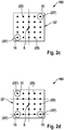
- Fig. 2c:
- schematische Darstellung von Projektionsflächen eines elektrisch kontaktierten Bauelementes bei einer dritten Ausführung einer Kontaktanordnung,
- Fig. 2d:
- schematische Darstellung von Projektionsflächen eines elektrisch kontaktierten Bauelementes bei einer vierten Ausführung einer Kontaktanordnung.
- In den Figuren sind funktional gleiche Bauelemente jeweils mit gleichen Bezugszeichen gekennzeichnet.
- In der
Fig. 1 ist eine erste Ausführung einer Kontaktanordnung 100 in einer seitlichen Schnittdarstellung gezeigt. Die Kontaktanordnung 100 umfasst hierbei zumindest einen Schaltungsträger 10, welcher eine Oberseite 11 und eine Unterseite 12 aufweist. Mit dem Schaltungsträger 10 ist zumindest ein elektrisches Bauelement 20 elektrisch kontaktiert. Die Oberseite 11 weist eine Vielzahl von Kontaktstellen auf (auch als Pads bezeichnet, nicht dargestellt), die mit komplementären Kontaktanschlüssen 25 des elektrischen Bauelements 20 elektrisch verbunden sind, beispielsweise mittels eines Lotmaterials. Die Kontaktanschlüsse 25 sind hierbei in einer Musteranordnung auf einer der Oberseite 11 zugewandten Bauteilelementenseite 22 angeordnet. In der Schnittdarstellung derFig. 1 sind lediglich eine Anzahl von Kontaktanschlüssen 25 dargestellt, die in einer Linie angeordnet sind. Mögliche Musteranordnungen werden noch später mit Hilfe derFig. 2a - 2d erläutert. - Der Schaltungsträger 10 weist eine Zugangsöffnung 15 auf, welche die Oberseite 11 und die Unterseite 12 durchdringt. Mittels der Zugangsöffnung 15 ist das Einbringen eines Füllmaterials 30 in einen zwischen dem elektronischen Bauelement 20 und dem Schaltungsträger 10 ausgebildeten Abstandsspalt 13 ermöglicht. Dies kann beispielhaft durch eine Füllvorrichtung 40 erfolgen, welche das Füllmaterial 30 mit Druck durch die Zugangsöffnung 15 einspritzt. Mit zunehmenden Füllgrad ist der Abstandsspalt 13 dann bevorzugt bis zu den Bauelementenrändern vollständig mit dem Füllmaterial 30 ausgefüllt (gestrichelt dargestellt). Die Zugangsöffnung 15 ist derart in dem Schaltungsträger 10 und in Bezug zu der Musteranordnung an Kontaktanschlüssen 25 angeordnet, dass zumindest ein Kontaktanschluss 25' zumindest teilweise oberhalb der Zugangsöffnung 15 freistehend, insbesondere zu dieser zentriert, angeordnet ist und dadurch frei von jeglicher elektrischer Kontaktierung ist. Die Anordnung der Zugangsöffnung ist weiter verdeutlicht in der
Fig. 2a gezeigt. Diese zeigt in einer senkrechten Sicht A auf die Oberseite 11 des Schaltungsträgers 10 lediglich die Projektionsfläche 22' der oben bezeichneten Bauelementenseite 22 und die sich aus einer Musteranordnung ergebenden Projektionsflächen der angeordneten Kontaktanschlüsse 25. Vereinfacht ist noch gestrichelt eine Berandung des Schaltungsträgers 10 gezeigt. Die Musteranordnung der Kontaktanschlüsse 25 ist beispielsweise gebildet als eine Anordnung der Kontaktanschlüsse 25 in einem Raster von parallelen Zeilen und parallelen Spalten, insbesondere in Form einer n x m-Matrix, wobei durch n beispielsweise die Anzahl an Spalten und durch m die Anzahl der Zeilen bezeichnet sind. Die Anzahl der Spalten n und/oder der Zeilen m ist jeweils beispielsweise >=3, bevorzugt >= 20, wie beispielsweise zwischen 20 und 60, insbesondere bis 100. Zur Verdeutlichung sind Rasterlinien dargestellt, wobei die Kontaktanschlüsse 25 bevorzugt in allen Schnittpunkten der Rasterlinien ausgebildet sind. Eine Musteranordnung kann alternativ auch in anderen Formen ausgebildet sein. Insgesamt weisen die in einer Spalte n in Linie angeordneten Kontaktanschlüsse 25 einen Pitchabstand pm auf und die in einer Zeile m angeordneten Kontaktanschlüsse 25 einen Pitchabstand pn auf. Die Pitchabstände pm und pn sind bevorzugt lediglich <= 2 mm groß, insbesondere <= 0,65 mm. In derFig. 2a ist auch die Berandung der Zugangsöffnung 15 ersichtlich, welche beispielsweise eine kreisrunde Fläche umschließt aufgrund einer zylindrischen Ausbildung der Zugangsöffnung 15. Es zeigt sich, dass in der Projektion in einer Gruppe von benachbarten Kontaktanschlüssen 25 die Anschlussfläche zumindest eines von drei nächst benachbarten Kontaktanschlüssen 25 innerhalb der Berandung der Zugangsöffnung 15 angeordnet ist. Demnach ist die betreffende Anschlussfläche des einen Kontaktanschlusses 25' in der Projektion vollständig von der Fläche der Zugangsöffnung 15 überdeckt. Alternativ kann auch nur eine teilweise Überdeckung vorliegen und/oder die Anschlussflächen von mehreren Kontaktanschlüssen 25' derartig vollständig oder teilweise überdeckt sein. Die Zugangsöffnung weist eine maximale lichte Weite d von >=2 mm, insbesondere von >=0,7 mm auf. Ferner ist die Zugangsöffnung 15 bevorzugt in oder zumindest in einem unmittelbaren Bereich des Flächenschwerpunktes S der Projektionsfläche 22' der Bauelementenseite 22 angeordnet. Auf diese Weise ergibt sich ein sehr zentraler Zugang des Füllmaterials 30 zum Befüllen des Abstandsspaltes 13. - Aus den
Fig. 2b - 2d gehen weitere mögliche Ausführungen einer Kontaktanordnung 100 hervor. Im Wesentlichen entsprechen diese der ersten Ausführung gemäß denFig. 1 und2a . Die Unterschiede zeigen sich lediglich wie nachfolgend aufgeführt (die Berandung des Schaltungsträger 10 ist zur Vereinfach nicht weiter abgebildet). - Die zweite Ausführung der Kontaktanordnung gemäß der
Fig. 2b weist insgesamt 3 Zugangsöffnungen 15 in dem Schaltungsträger 10 auf. Diese sind rotationssymmetrisch um den Flächenschwerpunkt S in 120° Winkelabständen zueinander angeordnet. Bevorzugt sind diese Zugangsöffnungen 15 in einem jeweiligen Abstand zu dem Flächenschwerpunkt S derart angeordnet, dass um deren jeweilige Öffnungsachse gleich große konzentrische Kreise sich jeweils in einem Punkt berühren (gestrichelt dargestellt), wobei eine Summe der gebildeten Kreisflächen min. 60% und max. 140% der projizierten Fläche 22' der Bauelementenseite 22 entsprechen. Zusätzlich kann auch eine vierte Zugangsöffnung wie bei der ersten Ausführung im Schwerpunkt S angeordnet sein (gestrichelt gezeichnet). Nur rein beispielhaft ist im Gegensatz zur Ausführung zurFig. 2a eine größere Anzahl an Kontaktanschlüssen 25 gezeigt. - Die dritte Ausführung der Kontaktanordnung ist in
Fig. 2c gezeigt. Diese zeigt im Gegensatz zu den vorhergehenden Ausführungsformen insgesamt zwei Zugangsöffnungen 15, die diagonal gegenüberliegend in Ausrichtung zu den Ecken der Projektionsfläche 22' der Bauelementenseite 22 angeordnet sind, insbesondere punkt- und/oder rotationssymmetrisch zum Flächenschwerpunkt S. - In der vierten Ausführung der Kontaktanordnung 100 sind insgesamt drei Zugangsöffnungen 15 in Ausrichtung zu den Ecken der Projektionsfläche 22' der Bauelementenseite 22 angeordnet, teilähnlich wie bei der dritten Ausführung.
- Grundsätzlich sind die gleiche Anzahl an Zugangsöffnungen 15 oder weitere in anderer Anordnung im Schaltungsträger 10 denkbar. Ebenso kann ein elektrisches Bauelement 20 alternativ oder zusätzlich auf der Unterseite 12 des Schaltungsträgers 10 elektrisch kontaktiert angeordnet sein. Bevorzugt weisen die kontaktierten Bauelemente 20 verschiedenster Ausführungen der Kontaktanordnung 100 eine Gehäuseform gemäß einer Ausführungsart von BGA (ball grid array), von LGA (land grid array), von PGA (pin grid array) oder von WLP (wafer level packaging) auf. In der Schnittdarstellung der
Fig. 1 sind beispielsweise Kontaktanschlüsse 25 eines BGA-Bauelementes gezeigt. Im Bereich der gezeigten Zugangsöffnung 15 verbleibt ein Abstandspalt zum elektrisch freiliegenden Ball 25', so dass ein Füllmaterial daran vorbeigeführt in den Abstandsspalt 13 gelangt.
Claims (10)
- Kontaktanordnung (100), umfassend einen Schaltungsträger (10) mit einer Ober- und einer Unterseite (11, 12) und zumindest ein elektronisches Bauelement (20), wobei der Schaltungsträger (10) zumindest Kontaktstellen auf der Oberseite (11) aufweist, die mit Kontaktanschlüssen (25) des elektronischen Bauelements (20) elektrisch kontaktiert sind, und einem Füllmaterial (30), welches einen Abstandsspalt (13) zwischen der Oberseite (11) des Schaltungsträgers (10) und dem elektronischen Bauelement (20) ausfüllt, wobei der Schaltungsträger (10) eine Zugangsöffnung (15) zum Einbringen des Füllmaterials (30) aufweist, wobei das elektronische Bauelement (20) auf einer der Oberseite (11) des Schaltungsträgers (20) zugewandten Bauelementenseite (22) eine Musteranordnung der Kontaktanschlüssen (25) aufweist,
dadurch gekennzeichnet, dass
eine Anschlussfläche von zumindest einem von drei nächst benachbarten Kontaktanschlüssen (25, 25') in einer senkrechten Projektion auf die Oberseite (11) von der Zugangsöffnung (15) zumindest teilweise überdeckt ist und der zur überdeckten Anschlussfläche zugehörige Kontaktanschluss (25') frei von einer elektrischen Kontaktierung ist. - Kontaktanordnung (100) nach Anspruch 1,
dadurch gekennzeichnet, dass
die überdeckte Anschlussfläche in der Projektion vollständig innerhalb der Zugangsöffnung (15) angeordnet ist. - Kontaktanordnung (100) nach Anspruch 1 oder 2,
dadurch gekennzeichnet, dass
die drei nächst benachbarten Kontaktanschlüsse (25, 25') in einer Linie angeordnet sind und der zur überdeckten Anschlussfläche zugehörige Kontaktanschluss (25') den mittleren Kontaktanschluss bildet. - Kontaktanordnung (100) nach einem der vorhergehenden Ansprüche,
dadurch gekennzeichnet, dass
die Musteranordnung der Kontaktanschlüsse (25, 25') gebildet ist als eine Anordnung der Kontaktanschlüsse in einem Raster von parallelen Zeilen und parallelen Spalten. - Kontaktanordnung (100) nach einem der vorhergehenden Ansprüche,
dadurch gekennzeichnet, dass
der zur überdeckten Anschlussfläche zugehörige Kontaktanschluss (25') zu zumindest einem der nächst benachbarten Kontaktanschlüsse (25), bevorzugt zu beiden nächst benachbarten Kontaktanschlüssen (25), einen Pitchabstand von <= 2 mm, insbesondere <= 0,65 mm, aufweist. - Kontaktanordnung (100) nach einem der vorhergehenden Ansprüche,
dadurch gekennzeichnet, dass
alle Kontaktanschlüsse (25, 25') der Musteranordnung, einen jeweils gleichen Pitchabstand zueinander aufweisen. - Kontaktanordnung (100) nach einem der vorhergehenden Ansprüche,
dadurch gekennzeichnet, dass
die Zugangsöffnung (15) eine maximale lichte Weite (d) von <= 2,0, insbesondere <= 0,7 mm, aufweist und/oder die Zugangsöffnung zylindrisch ist und einen Öffnungsdurchmesser (d) von <= 2,0, insbesondere <= 0,7 mm, oder mindestens das doppeltem Maß des Abstandsspaltes (13), aufweist. - Kontaktanordnung (100) nach einem der vorhergehenden Ansprüche,
dadurch gekennzeichnet, dass
die die Musteranordnung der Kontaktanschlüsse (25, 25') aufweisende Bauelementenseite (22) in der Projektion einen Flächenschwerpunkt (S) in der projizierten Fläche (22') aufweist und zumindest eine Zugangsöffnung (15) im Bereich des Flächenschwerpunktes (S) angeordnet ist und/oder zwei oder mehr Zugangsöffnungen (15) punkt- und/oder rotationssymmetrisch um den Flächenschwerpunkt (S) angeordnet sind. - Kontaktanordnung (100) nach Anspruch 8,
dadurch gekennzeichnet, dass
die punkt- und/oder rotationssymmetrisch angeordneten zwei oder mehr Zugangsöffnungen (15) derart zueinander angeordnet sind, dass um deren jeweilige Öffnungsachse gleich große konzentrische Kreise sich jeweils in einem Punkt berühren, wobei eine Summe der gebildeten Kreisflächen min. 60% und max. 140% der projizierten Fläche (22') der Bauelementenseite entsprechen. - Kontaktanordnung (100) nach einem der vorhergehenden Ansprüche,
dadurch gekennzeichnet, dass
das elektronische Bauelement (20) als Gehäuseform eine Ausführungsart von BGA (ball grid array), von LGA (land grid array), von PGA (pin grid array) oder von WLP (wafer level packaging) aufweist.
Applications Claiming Priority (2)
| Application Number | Priority Date | Filing Date | Title |
|---|---|---|---|
| DE102017204842.5A DE102017204842A1 (de) | 2017-03-22 | 2017-03-22 | Kontaktanordnung |
| PCT/EP2018/056193 WO2018172137A1 (de) | 2017-03-22 | 2018-03-13 | Kontaktanordnung |
Publications (2)
| Publication Number | Publication Date |
|---|---|
| EP3603356A1 EP3603356A1 (de) | 2020-02-05 |
| EP3603356B1 true EP3603356B1 (de) | 2021-05-12 |
Family
ID=61655774
Family Applications (1)
| Application Number | Title | Priority Date | Filing Date |
|---|---|---|---|
| EP18711301.4A Active EP3603356B1 (de) | 2017-03-22 | 2018-03-13 | Kontaktanordnung |
Country Status (4)
| Country | Link |
|---|---|
| EP (1) | EP3603356B1 (de) |
| CN (1) | CN110419270B (de) |
| DE (1) | DE102017204842A1 (de) |
| WO (1) | WO2018172137A1 (de) |
Families Citing this family (1)
| Publication number | Priority date | Publication date | Assignee | Title |
|---|---|---|---|---|
| EP4468829A1 (de) * | 2023-05-24 | 2024-11-27 | Mettler-Toledo GmbH | Leiterplattenanordnung |
Family Cites Families (8)
| Publication number | Priority date | Publication date | Assignee | Title |
|---|---|---|---|---|
| CH660551GA3 (de) | 1982-12-27 | 1987-05-15 | ||
| US5766982A (en) | 1996-03-07 | 1998-06-16 | Micron Technology, Inc. | Method and apparatus for underfill of bumped or raised die |
| DE19810060B4 (de) * | 1997-05-07 | 2005-10-13 | Fraunhofer-Gesellschaft zur Förderung der angewandten Forschung e.V. | Verfahren zur Verbindung eines Bauelements mit einem Substrat und eine damit hergestellte elektrische Schaltung |
| JP2001053411A (ja) * | 1999-08-16 | 2001-02-23 | Hitachi Kokusai Electric Inc | プリント基板に対して実装部材を固定する方法、および、同固定構造 |
| JP2004288834A (ja) * | 2003-03-20 | 2004-10-14 | Fujitsu Ltd | 電子部品の実装方法、実装構造及びパッケージ基板 |
| US7791209B2 (en) | 2008-03-12 | 2010-09-07 | International Business Machines Corporation | Method of underfill air vent for flipchip BGA |
| TW201207961A (en) * | 2010-08-04 | 2012-02-16 | Global Unichip Corp | Semiconductor package device using underfill material and packaging method thereof |
| US9917068B2 (en) * | 2014-03-14 | 2018-03-13 | Taiwan Semiconductor Manufacturing Company | Package substrates, packaged semiconductor devices, and methods of packaging semiconductor devices |
-
2017
- 2017-03-22 DE DE102017204842.5A patent/DE102017204842A1/de not_active Withdrawn
-
2018
- 2018-03-13 WO PCT/EP2018/056193 patent/WO2018172137A1/de not_active Ceased
- 2018-03-13 EP EP18711301.4A patent/EP3603356B1/de active Active
- 2018-03-13 CN CN201880018572.9A patent/CN110419270B/zh active Active
Also Published As
| Publication number | Publication date |
|---|---|
| CN110419270A (zh) | 2019-11-05 |
| CN110419270B (zh) | 2022-05-31 |
| WO2018172137A1 (de) | 2018-09-27 |
| EP3603356A1 (de) | 2020-02-05 |
| DE102017204842A1 (de) | 2018-09-27 |
Similar Documents
| Publication | Publication Date | Title |
|---|---|---|
| DE102012100793B4 (de) | Halbleitervorrichtung, montierte Halbleitervorrichtung und Verfahren zum Herstellen und Montieren derselben | |
| DE102014019418B4 (de) | Design einer Kontaktstellenstruktur in einem Fan-out-Gehäuse | |
| DE102014100512A1 (de) | Chip-gehäuse mit anschlusspads mit unterschiedlichen formfaktoren | |
| WO1996023230A1 (de) | Mikromechanisches bauelement | |
| DE102005041058A1 (de) | Verfahren zur Herstellung einer mehrschichtigen Karte | |
| DE112017004053B4 (de) | Optoelektronischer Halbleiterchip | |
| DE102017223689A1 (de) | Halbleitervorrichtungen mit Hochfrequenzleitungselementen und zugehörige Herstellungsverfahren | |
| DE102013103138A1 (de) | Gedrehte Halbleiterbauelementgehäuse auf Wafer-Ebene vom Fan-Out-Typ und Verfahren zum Herstellen gedrehter Halbleiterbauelementgehäuse auf Wafer-Ebene vom Fan-Out-Typ | |
| EP3603356B1 (de) | Kontaktanordnung | |
| DE102012103242B4 (de) | Chip-Anordnungen und Verfahren zum Herstellen einer Chip-Anordnung | |
| DE19962702B4 (de) | Prüfsockel einer BGA-Vorrichtung | |
| DE10217566A1 (de) | Halbleiterbauelement mit integrierter, eine Mehrzahl an Metallisierungsebenen aufweisende Kapazitätsstruktur | |
| EP0351531A2 (de) | Elektronische Baueinheit | |
| DE10259634B4 (de) | Verfahren zur Herstellung von Kontakten auf einem Wafer | |
| DE102004027788A1 (de) | Halbleiterbasisbauteil mit Umverdrahtungssubstrat und Zwischenverdrahtungsplatte für einen Halbleiterbauteilstapel sowie Verfahren zu deren Herstellung | |
| WO2024175462A1 (de) | Verfahren zum herstellen eines optoelektronischen bauelements | |
| DE102016113093B4 (de) | Halbleiterchip mit einer dichten anordnung von kontaktanschlüssen | |
| DE10132668A1 (de) | Halbleitervorrichtung mit definierter Eingangs- /Ausgangsblockgröße und Verfahren zu deren Entwicklung | |
| WO2009153356A1 (de) | Halbleiterbauelement mit kreuzungen von isolationsgräben | |
| EP1390978A2 (de) | Halbleiterspeichereinrichtung sowie verfahren zu deren herstellung | |
| DE10126296B4 (de) | Verfahren zur Herstellung eines elektronischen Bauelements | |
| DE10136152A1 (de) | Halbleiterbauteil | |
| DE102020116233A1 (de) | Schaltungsträger mit Anschlussflächenfeld und Verfahren zum Herstellen eines Anschlussflächenfelds auf einem Schaltungsträger | |
| DE10347622B4 (de) | Substrat mit Lötpad zur Herstellung einer Lötverbindung | |
| EP2263094B1 (de) | Prüfkontaktanordnung |
Legal Events
| Date | Code | Title | Description |
|---|---|---|---|
| STAA | Information on the status of an ep patent application or granted ep patent |
Free format text: STATUS: UNKNOWN |
|
| STAA | Information on the status of an ep patent application or granted ep patent |
Free format text: STATUS: THE INTERNATIONAL PUBLICATION HAS BEEN MADE |
|
| PUAI | Public reference made under article 153(3) epc to a published international application that has entered the european phase |
Free format text: ORIGINAL CODE: 0009012 |
|
| STAA | Information on the status of an ep patent application or granted ep patent |
Free format text: STATUS: REQUEST FOR EXAMINATION WAS MADE |
|
| 17P | Request for examination filed |
Effective date: 20191022 |
|
| AK | Designated contracting states |
Kind code of ref document: A1 Designated state(s): AL AT BE BG CH CY CZ DE DK EE ES FI FR GB GR HR HU IE IS IT LI LT LU LV MC MK MT NL NO PL PT RO RS SE SI SK SM TR |
|
| AX | Request for extension of the european patent |
Extension state: BA ME |
|
| RAP1 | Party data changed (applicant data changed or rights of an application transferred) |
Owner name: ROBERT BOSCH GMBH |
|
| DAV | Request for validation of the european patent (deleted) | ||
| DAX | Request for extension of the european patent (deleted) | ||
| GRAP | Despatch of communication of intention to grant a patent |
Free format text: ORIGINAL CODE: EPIDOSNIGR1 |
|
| STAA | Information on the status of an ep patent application or granted ep patent |
Free format text: STATUS: GRANT OF PATENT IS INTENDED |
|
| INTG | Intention to grant announced |
Effective date: 20201125 |
|
| GRAS | Grant fee paid |
Free format text: ORIGINAL CODE: EPIDOSNIGR3 |
|
| GRAA | (expected) grant |
Free format text: ORIGINAL CODE: 0009210 |
|
| STAA | Information on the status of an ep patent application or granted ep patent |
Free format text: STATUS: THE PATENT HAS BEEN GRANTED |
|
| AK | Designated contracting states |
Kind code of ref document: B1 Designated state(s): AL AT BE BG CH CY CZ DE DK EE ES FI FR GB GR HR HU IE IS IT LI LT LU LV MC MK MT NL NO PL PT RO RS SE SI SK SM TR |
|
| REG | Reference to a national code |
Ref country code: GB Ref legal event code: FG4D Free format text: NOT ENGLISH |
|
| REG | Reference to a national code |
Ref country code: CH Ref legal event code: EP |
|
| REG | Reference to a national code |
Ref country code: DE Ref legal event code: R096 Ref document number: 502018005237 Country of ref document: DE |
|
| REG | Reference to a national code |
Ref country code: IE Ref legal event code: FG4D Free format text: LANGUAGE OF EP DOCUMENT: GERMAN |
|
| REG | Reference to a national code |
Ref country code: AT Ref legal event code: REF Ref document number: 1393068 Country of ref document: AT Kind code of ref document: T Effective date: 20210615 |
|
| REG | Reference to a national code |
Ref country code: LT Ref legal event code: MG9D |
|
| REG | Reference to a national code |
Ref country code: NL Ref legal event code: MP Effective date: 20210512 |
|
| PG25 | Lapsed in a contracting state [announced via postgrant information from national office to epo] |
Ref country code: LT Free format text: LAPSE BECAUSE OF FAILURE TO SUBMIT A TRANSLATION OF THE DESCRIPTION OR TO PAY THE FEE WITHIN THE PRESCRIBED TIME-LIMIT Effective date: 20210512 Ref country code: HR Free format text: LAPSE BECAUSE OF FAILURE TO SUBMIT A TRANSLATION OF THE DESCRIPTION OR TO PAY THE FEE WITHIN THE PRESCRIBED TIME-LIMIT Effective date: 20210512 Ref country code: FI Free format text: LAPSE BECAUSE OF FAILURE TO SUBMIT A TRANSLATION OF THE DESCRIPTION OR TO PAY THE FEE WITHIN THE PRESCRIBED TIME-LIMIT Effective date: 20210512 Ref country code: BG Free format text: LAPSE BECAUSE OF FAILURE TO SUBMIT A TRANSLATION OF THE DESCRIPTION OR TO PAY THE FEE WITHIN THE PRESCRIBED TIME-LIMIT Effective date: 20210812 |
|
| PG25 | Lapsed in a contracting state [announced via postgrant information from national office to epo] |
Ref country code: SE Free format text: LAPSE BECAUSE OF FAILURE TO SUBMIT A TRANSLATION OF THE DESCRIPTION OR TO PAY THE FEE WITHIN THE PRESCRIBED TIME-LIMIT Effective date: 20210512 Ref country code: RS Free format text: LAPSE BECAUSE OF FAILURE TO SUBMIT A TRANSLATION OF THE DESCRIPTION OR TO PAY THE FEE WITHIN THE PRESCRIBED TIME-LIMIT Effective date: 20210512 Ref country code: PT Free format text: LAPSE BECAUSE OF FAILURE TO SUBMIT A TRANSLATION OF THE DESCRIPTION OR TO PAY THE FEE WITHIN THE PRESCRIBED TIME-LIMIT Effective date: 20210913 Ref country code: PL Free format text: LAPSE BECAUSE OF FAILURE TO SUBMIT A TRANSLATION OF THE DESCRIPTION OR TO PAY THE FEE WITHIN THE PRESCRIBED TIME-LIMIT Effective date: 20210512 Ref country code: NO Free format text: LAPSE BECAUSE OF FAILURE TO SUBMIT A TRANSLATION OF THE DESCRIPTION OR TO PAY THE FEE WITHIN THE PRESCRIBED TIME-LIMIT Effective date: 20210812 Ref country code: LV Free format text: LAPSE BECAUSE OF FAILURE TO SUBMIT A TRANSLATION OF THE DESCRIPTION OR TO PAY THE FEE WITHIN THE PRESCRIBED TIME-LIMIT Effective date: 20210512 Ref country code: IS Free format text: LAPSE BECAUSE OF FAILURE TO SUBMIT A TRANSLATION OF THE DESCRIPTION OR TO PAY THE FEE WITHIN THE PRESCRIBED TIME-LIMIT Effective date: 20210912 Ref country code: GR Free format text: LAPSE BECAUSE OF FAILURE TO SUBMIT A TRANSLATION OF THE DESCRIPTION OR TO PAY THE FEE WITHIN THE PRESCRIBED TIME-LIMIT Effective date: 20210813 |
|
| PG25 | Lapsed in a contracting state [announced via postgrant information from national office to epo] |
Ref country code: NL Free format text: LAPSE BECAUSE OF FAILURE TO SUBMIT A TRANSLATION OF THE DESCRIPTION OR TO PAY THE FEE WITHIN THE PRESCRIBED TIME-LIMIT Effective date: 20210512 |
|
| PG25 | Lapsed in a contracting state [announced via postgrant information from national office to epo] |
Ref country code: EE Free format text: LAPSE BECAUSE OF FAILURE TO SUBMIT A TRANSLATION OF THE DESCRIPTION OR TO PAY THE FEE WITHIN THE PRESCRIBED TIME-LIMIT Effective date: 20210512 Ref country code: ES Free format text: LAPSE BECAUSE OF FAILURE TO SUBMIT A TRANSLATION OF THE DESCRIPTION OR TO PAY THE FEE WITHIN THE PRESCRIBED TIME-LIMIT Effective date: 20210512 Ref country code: SM Free format text: LAPSE BECAUSE OF FAILURE TO SUBMIT A TRANSLATION OF THE DESCRIPTION OR TO PAY THE FEE WITHIN THE PRESCRIBED TIME-LIMIT Effective date: 20210512 Ref country code: SK Free format text: LAPSE BECAUSE OF FAILURE TO SUBMIT A TRANSLATION OF THE DESCRIPTION OR TO PAY THE FEE WITHIN THE PRESCRIBED TIME-LIMIT Effective date: 20210512 Ref country code: CZ Free format text: LAPSE BECAUSE OF FAILURE TO SUBMIT A TRANSLATION OF THE DESCRIPTION OR TO PAY THE FEE WITHIN THE PRESCRIBED TIME-LIMIT Effective date: 20210512 Ref country code: DK Free format text: LAPSE BECAUSE OF FAILURE TO SUBMIT A TRANSLATION OF THE DESCRIPTION OR TO PAY THE FEE WITHIN THE PRESCRIBED TIME-LIMIT Effective date: 20210512 Ref country code: RO Free format text: LAPSE BECAUSE OF FAILURE TO SUBMIT A TRANSLATION OF THE DESCRIPTION OR TO PAY THE FEE WITHIN THE PRESCRIBED TIME-LIMIT Effective date: 20210512 |
|
| REG | Reference to a national code |
Ref country code: DE Ref legal event code: R097 Ref document number: 502018005237 Country of ref document: DE |
|
| PLBE | No opposition filed within time limit |
Free format text: ORIGINAL CODE: 0009261 |
|
| STAA | Information on the status of an ep patent application or granted ep patent |
Free format text: STATUS: NO OPPOSITION FILED WITHIN TIME LIMIT |
|
| 26N | No opposition filed |
Effective date: 20220215 |
|
| PG25 | Lapsed in a contracting state [announced via postgrant information from national office to epo] |
Ref country code: IS Free format text: LAPSE BECAUSE OF FAILURE TO SUBMIT A TRANSLATION OF THE DESCRIPTION OR TO PAY THE FEE WITHIN THE PRESCRIBED TIME-LIMIT Effective date: 20210912 Ref country code: AL Free format text: LAPSE BECAUSE OF FAILURE TO SUBMIT A TRANSLATION OF THE DESCRIPTION OR TO PAY THE FEE WITHIN THE PRESCRIBED TIME-LIMIT Effective date: 20210512 |
|
| PG25 | Lapsed in a contracting state [announced via postgrant information from national office to epo] |
Ref country code: IT Free format text: LAPSE BECAUSE OF FAILURE TO SUBMIT A TRANSLATION OF THE DESCRIPTION OR TO PAY THE FEE WITHIN THE PRESCRIBED TIME-LIMIT Effective date: 20210512 |
|
| PG25 | Lapsed in a contracting state [announced via postgrant information from national office to epo] |
Ref country code: MC Free format text: LAPSE BECAUSE OF FAILURE TO SUBMIT A TRANSLATION OF THE DESCRIPTION OR TO PAY THE FEE WITHIN THE PRESCRIBED TIME-LIMIT Effective date: 20210512 |
|
| REG | Reference to a national code |
Ref country code: CH Ref legal event code: PL |
|
| GBPC | Gb: european patent ceased through non-payment of renewal fee |
Effective date: 20220313 |
|
| REG | Reference to a national code |
Ref country code: BE Ref legal event code: MM Effective date: 20220331 |
|
| PG25 | Lapsed in a contracting state [announced via postgrant information from national office to epo] |
Ref country code: LU Free format text: LAPSE BECAUSE OF NON-PAYMENT OF DUE FEES Effective date: 20220313 Ref country code: LI Free format text: LAPSE BECAUSE OF NON-PAYMENT OF DUE FEES Effective date: 20220331 Ref country code: IE Free format text: LAPSE BECAUSE OF NON-PAYMENT OF DUE FEES Effective date: 20220313 Ref country code: GB Free format text: LAPSE BECAUSE OF NON-PAYMENT OF DUE FEES Effective date: 20220313 Ref country code: FR Free format text: LAPSE BECAUSE OF NON-PAYMENT OF DUE FEES Effective date: 20220331 Ref country code: CH Free format text: LAPSE BECAUSE OF NON-PAYMENT OF DUE FEES Effective date: 20220331 |
|
| PG25 | Lapsed in a contracting state [announced via postgrant information from national office to epo] |
Ref country code: BE Free format text: LAPSE BECAUSE OF NON-PAYMENT OF DUE FEES Effective date: 20220331 |
|
| P01 | Opt-out of the competence of the unified patent court (upc) registered |
Effective date: 20230509 |
|
| PG25 | Lapsed in a contracting state [announced via postgrant information from national office to epo] |
Ref country code: MK Free format text: LAPSE BECAUSE OF FAILURE TO SUBMIT A TRANSLATION OF THE DESCRIPTION OR TO PAY THE FEE WITHIN THE PRESCRIBED TIME-LIMIT Effective date: 20210512 Ref country code: CY Free format text: LAPSE BECAUSE OF FAILURE TO SUBMIT A TRANSLATION OF THE DESCRIPTION OR TO PAY THE FEE WITHIN THE PRESCRIBED TIME-LIMIT Effective date: 20210512 |
|
| REG | Reference to a national code |
Ref country code: AT Ref legal event code: MM01 Ref document number: 1393068 Country of ref document: AT Kind code of ref document: T Effective date: 20230313 |
|
| PG25 | Lapsed in a contracting state [announced via postgrant information from national office to epo] |
Ref country code: HU Free format text: LAPSE BECAUSE OF FAILURE TO SUBMIT A TRANSLATION OF THE DESCRIPTION OR TO PAY THE FEE WITHIN THE PRESCRIBED TIME-LIMIT; INVALID AB INITIO Effective date: 20180313 |
|
| PG25 | Lapsed in a contracting state [announced via postgrant information from national office to epo] |
Ref country code: TR Free format text: LAPSE BECAUSE OF FAILURE TO SUBMIT A TRANSLATION OF THE DESCRIPTION OR TO PAY THE FEE WITHIN THE PRESCRIBED TIME-LIMIT Effective date: 20210512 |
|
| PG25 | Lapsed in a contracting state [announced via postgrant information from national office to epo] |
Ref country code: AT Free format text: LAPSE BECAUSE OF NON-PAYMENT OF DUE FEES Effective date: 20230313 |
|
| PG25 | Lapsed in a contracting state [announced via postgrant information from national office to epo] |
Ref country code: AT Free format text: LAPSE BECAUSE OF NON-PAYMENT OF DUE FEES Effective date: 20230313 |
|
| PG25 | Lapsed in a contracting state [announced via postgrant information from national office to epo] |
Ref country code: MT Free format text: LAPSE BECAUSE OF FAILURE TO SUBMIT A TRANSLATION OF THE DESCRIPTION OR TO PAY THE FEE WITHIN THE PRESCRIBED TIME-LIMIT Effective date: 20210512 |
|
| PGFP | Annual fee paid to national office [announced via postgrant information from national office to epo] |
Ref country code: DE Payment date: 20250522 Year of fee payment: 8 |
|
| PGFP | Annual fee paid to national office [announced via postgrant information from national office to epo] |
Ref country code: AT Payment date: 20260410 Year of fee payment: 5 |