EP3595170B1 - Anschlusskasten vom typ eines niederdruck-chip-gehäuses und verarbeitungsverfahren dafür für solarstromerzeugungsanordnung - Google Patents
Anschlusskasten vom typ eines niederdruck-chip-gehäuses und verarbeitungsverfahren dafür für solarstromerzeugungsanordnung Download PDFInfo
- Publication number
- EP3595170B1 EP3595170B1 EP17899848.0A EP17899848A EP3595170B1 EP 3595170 B1 EP3595170 B1 EP 3595170B1 EP 17899848 A EP17899848 A EP 17899848A EP 3595170 B1 EP3595170 B1 EP 3595170B1
- Authority
- EP
- European Patent Office
- Prior art keywords
- copper conductors
- junction box
- power generation
- chips
- solar power
- Prior art date
- Legal status (The legal status is an assumption and is not a legal conclusion. Google has not performed a legal analysis and makes no representation as to the accuracy of the status listed.)
- Active
Links
Images






Classifications
-
- H—ELECTRICITY
- H02—GENERATION; CONVERSION OR DISTRIBUTION OF ELECTRIC POWER
- H02S—GENERATION OF ELECTRIC POWER BY CONVERSION OF INFRARED RADIATION, VISIBLE LIGHT OR ULTRAVIOLET LIGHT, e.g. USING PHOTOVOLTAIC [PV] MODULES
- H02S40/00—Components or accessories in combination with PV modules, not provided for in groups H02S10/00 - H02S30/00
- H02S40/30—Electrical components
- H02S40/34—Electrical components comprising specially adapted electrical connection means to be structurally associated with the PV module, e.g. junction boxes
-
- H—ELECTRICITY
- H10—SEMICONDUCTOR DEVICES; ELECTRIC SOLID-STATE DEVICES NOT OTHERWISE PROVIDED FOR
- H10F—INORGANIC SEMICONDUCTOR DEVICES SENSITIVE TO INFRARED RADIATION, LIGHT, ELECTROMAGNETIC RADIATION OF SHORTER WAVELENGTH OR CORPUSCULAR RADIATION
- H10F71/00—Manufacture or treatment of devices covered by this subclass
-
- H—ELECTRICITY
- H10—SEMICONDUCTOR DEVICES; ELECTRIC SOLID-STATE DEVICES NOT OTHERWISE PROVIDED FOR
- H10F—INORGANIC SEMICONDUCTOR DEVICES SENSITIVE TO INFRARED RADIATION, LIGHT, ELECTROMAGNETIC RADIATION OF SHORTER WAVELENGTH OR CORPUSCULAR RADIATION
- H10F77/00—Constructional details of devices covered by this subclass
- H10F77/60—Arrangements for cooling, heating, ventilating or compensating for temperature fluctuations
- H10F77/63—Arrangements for cooling directly associated or integrated with photovoltaic cells, e.g. heat sinks directly associated with the photovoltaic cells or integrated Peltier elements for active cooling
-
- H—ELECTRICITY
- H10—SEMICONDUCTOR DEVICES; ELECTRIC SOLID-STATE DEVICES NOT OTHERWISE PROVIDED FOR
- H10F—INORGANIC SEMICONDUCTOR DEVICES SENSITIVE TO INFRARED RADIATION, LIGHT, ELECTROMAGNETIC RADIATION OF SHORTER WAVELENGTH OR CORPUSCULAR RADIATION
- H10F77/00—Constructional details of devices covered by this subclass
- H10F77/93—Interconnections
- H10F77/933—Interconnections for devices having potential barriers
- H10F77/935—Interconnections for devices having potential barriers for photovoltaic devices or modules
- H10F77/937—Busbar structures for modules
-
- Y—GENERAL TAGGING OF NEW TECHNOLOGICAL DEVELOPMENTS; GENERAL TAGGING OF CROSS-SECTIONAL TECHNOLOGIES SPANNING OVER SEVERAL SECTIONS OF THE IPC; TECHNICAL SUBJECTS COVERED BY FORMER USPC CROSS-REFERENCE ART COLLECTIONS [XRACs] AND DIGESTS
- Y02—TECHNOLOGIES OR APPLICATIONS FOR MITIGATION OR ADAPTATION AGAINST CLIMATE CHANGE
- Y02E—REDUCTION OF GREENHOUSE GAS [GHG] EMISSIONS, RELATED TO ENERGY GENERATION, TRANSMISSION OR DISTRIBUTION
- Y02E10/00—Energy generation through renewable energy sources
- Y02E10/50—Photovoltaic [PV] energy
Definitions
- the present invention relates to a junction box for a solar power generation assembly, particularly to a low-pressure chip packaging type junction box for a solar power generation assembly and a processing method thereof.
- a junction box for a solar power generation assembly is an important component installed in a solar power generation assembly. It plays a role in providing bypass protection for cells in the assembly and transmitting out power generated by the assembly.
- a solar power system connects a number of power generation assemblies in series and/or parallel via output cables in the junction boxes of the assemblies as well as connectors to realize power generation in high power, and provide power for users or connects the grid to supply power through power accumulation or inversion.
- the solar power generation assemblies in a solar power station system generate power under normal irradiation of sunlight and output electric energy, but when the sunlight irradiating a location of a power generation assembly is blocked by an object or a shadow of an object, the state of the silicon cell at this location will be changed from a power generation state into a resistance state.
- Other power generation assemblies connected to the silicon cell in series generate power normally under irradiation of sunlight and current passing the cell in a resistance state will generate large heat, burning down the cell and backing sheet of the assembly. This phenomenon is called hot spots of assemblies.
- a bypass diode is reversely connected in parallel with each silicon cell pack in solar power generation assemblies. When conditions for hot spots appear, the diode is connected in a normal direction and current is output via the bypass diode, thereby protecting the silicon cells from burn-down and the safety of the power generation assembly.
- bypass diodes are designed to be installed inside a junction box.
- three bypass diodes are typically installed in a common junction box, and each of them provides bypass protection for one third of the cells in the solar power generation assembly. Therefore, junction boxes for solar power generation assemblies simultaneously have functions of bypass protection and power output.
- junction boxes have undergone multiple improvements and developments.
- junction boxes are known from CN 104 579 158 A and JP 2005-252303 A .
- a junction box made in the prior art typically comprises an individual diode packaging device, a junction box body (box body and box cover), internal copper conducting heat sinks (copper conductors), output cables and connectors.
- Diodes are assembled by means of buckling or surface-mounted diodes are used, which are assembled by means of reflow soldering to copper conducting heat sinks inside the junction box; and the copper conducting heat sinks assembled with the diodes are installed inside the junction box body by means of hot riveting of plastics. Therefore, the manufacturing and installation processes of the junction box have many steps and are labor consuming.
- junction boxes produced in the prior art meet with difficulty in solving problems about sealing performance, temperature rise and internal gas expansion.
- the solution is to integrate three diode chips into an injection molding body. It can simplify the process steps of diode soldering and assembly of the junction box manufacturer.
- the module is fixed inside a junction box still by mounting method, sealant still needs to be filled in the inner chamber of the box body after the solar power assembly manufacturer installs the junction box into a power generation assembly, and the product does not have obvious advantages in production and application.
- the photovoltaic bypass diode module is fixed and connected to the junction box body via a plastic tray in a buckled manner.
- the limited heat dissipation space inside the junction box cannot be effectively utilized, thus limiting the passing capacity of working current.
- Complex production equipment is required in the production and application of junction boxes to achieve automatic assembly.
- Photovoltaic module products have the following defects in actual production and application:
- the present invention provides a low-pressure chip packaging type junction box for a solar power generation assembly and a processing method thereof, which can solve problems of large stress, high local temperature and uneven heat dissipation of the photovoltaic module, a low utilization rate of the internal heat dissipation space of the junction box and large investment in product development, integrate techniques relating to development and manufacturing of junction boxes with semiconductor packaging techniques to effectively enhance product performance and meanwhile reduce product cost and development cost and increase a degree of product automation.
- the low-pressure chip packaging type junction box for a solar power generation assembly comprises a box body, N chips, N connection members, and N+1 copper conductors, where N ⁇ 1,
- a process connection ring is arranged between at least two copper conductors.
- connection positions connecting the output end are further arranged on the first and the last copper conductors.
- the chips are arranged on two sides of the transverse bar respectively.
- Busbar guide holes are arranged on the transverse bar and run through the transverse bar from a back face of the box body; the lower openings of the busbar guide holes are large and the upper openings are small;
- Threading holes corresponding to the busbar through holes are arranged on the lead-out positions of the copper conductors.
- the processing method of a low-pressure chip packaging type junction box for a solar power generation assembly comprises the following steps:
- the process connecting structure at step 1) is a process connecting strip, which is located on a transverse bar,
- process connecting strips between adjacent copper conductors are cut off by blanking machine.
- the process connecting structure at step 1) is a process connection ring
- a heat sink is further comprised, which is packaged inside epoxy resin adhesive.
- the present invention designs the box body of the junction box into a plastic body having one or more adhesive storage slot with an opening top (i.e., accommodation recess); and determines the number of accommodation recesses according to the requirements of the junction box model and the requirements of heat dissipation distribution.
- accommodation recesses are arranged in two lines
- a transverse bar is arranged between two lines of accommodation recesses
- busbar guide holes are arranged on the transverse bar
- threading holes are arranged on lead-out positions of copper conductors so as to place a busbar according to user's application.
- chip installation positions are arranged on copper conductors and lead-out positions are arranged at a top surface of a transverse bar so that local copper conductors carrying diode chips by means of soldering sink through bending to enable the chips and partial copper conductors to be inlaid in corresponding accommodation recesses.
- epoxy resin adhesive with high thermal conductivity and high mechanical strength is potted into the accommodation recesses.
- the diode chips are sealed for protection, and the copper conductors are also fixed to the junction box body to form a junction box;
- N+1 copper conductors are connected in series by means of the chips and the connection members.
- the present invention designs process connection rings or process connecting strips among copper conductors during punching of the copper conductors so that a plurality of copper conductors temporarily forms an integral body. After chip soldering, potting and curing, the process connection rings or process connecting strips are removed by means of drilling or punching.
- the present invention steps over a packaging and manufacturing process of individually packaged diode junction boxes and photovoltaic module junction boxes, and skips work content such as secondary soldering and secondary assembly.
- the present invention integrates design and manufacturing of junction boxes with semiconductor diode packaging techniques and avoids potential quality hazard of junction box products arising from secondary soldering and installation; greatly raises development speed of junction boxes; saves the processes of mutual running-in and adjustment of the junction box manufacturer and the semiconductor diode packaging manufacturing; and facilitates a more compact structure of the junction box products, more reasonable use of materials, faster development of products, easier realization of automated production, lower product manufacturing cost and stronger market competitiveness.
- 1 denotes a box body
- 11 denotes an accommodation recess
- 12 denotes a transverse bar
- 120 denotes a busbar guide hole
- 13 denotes a positioning stud
- 14 denotes a conical blind hole
- 2 denotes a chip
- 3 denotes a connection member
- 4 denotes a copper conductor
- 41 denotes an installation hole
- 42 denotes a lead-out position
- 420 denotes a threading hole
- 43 denotes a connection position
- 5 denotes a potting adhesive
- 6 denotes a process connecting strip
- 7 denotes a process connection ring
- 8 denotes a heat sink
- 9 denotes a copper conductor frame
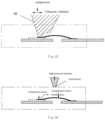
- 10 denotes an ultrasonic bonding tool.
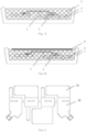
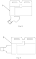
- the present invention as shown in FIGS. 1-34 , comprises a box body 1, N chips 2, N connection members 3 and N+1 copper conductors 4, with N ⁇ 1. At least one accommodation recess 11 is arranged at the box body, and a transverse bar 12 with a top surface higher than a bottom of the accommodation recess is arranged on the box body;
- Sinking copper conductors are made of red copper, brass or alloy copper through punching and bending.
- the lower plane after bending is a sinking location.
- Each copper conductor has one or more sinking location; the sinking locations are distributed on one side or a few sides or at a middle position of the copper conductor.
- chip installation positions are arranged on one of the two copper conductors, and lead-out positions are arranged on both of the copper conductors;
- the installation positions at the copper conductors, the chips and the connection members are potted, fixed and packaged within the accommodation recess by means of a potting adhesive 5, and the lead-out positions of the copper conductors are located above the transverse bar and higher than a top surface of the potting adhesive.
- a process connecting strip 6 is arranged between adjacent copper conductors so that a plurality of copper conductors temporarily forms an integral body to eliminate a pull stress on the chips resulting from relative movement of the copper conductors in the manufacturing process.
- a process connection ring 7 is arranged between at least two copper conductors so that a plurality of copper conductors temporarily forms an integral body to eliminate a pull stress on the chips resulting from relative movement of the copper conductors in the manufacturing process.
- connection positions connecting the output end are further arranged on the first and the last copper conductors.
- a clearance is arranged between copper conductors, which are electrically connected by means of chips and connection members, wherein the first copper conductor has an anode cable lead-out end and the last copper conductor has a cathode cable lead-out end, and the anode cable lead-out end and the cathode cable lead-out end are both arranged outside the box body;
- Busbar guide holes 120 are arranged on the transverse bar 12 and run through the transverse bar from a back face of the box body; and the lower openings of the busbar guide holes are large and the upper openings are small to play a guiding role and facilitate placement of a busbar; Threading holes 420 corresponding to the busbar guide holes are arranged on the lead-out positions 42 of the copper conductors.
- Threading holes and solder pads for customer's installation and soldering of a busbar are arranged on upper-layer stepped planes (i.e. lead-out positions) of sinking copper conductors; for copper conductors with one sinking location, threading holes and solder pads for customer's installation and soldering of a busbar are arranged on one side of the copper conductors; for copper conductors with two or more sinking locations, threading holes and solder pads for customer's installation and soldering of a busbar are arranged in the middle of the copper conductors.
- the processing method of a low-pressure chip packaging type junction box for a solar power generation assembly comprises the following steps:
- the process connecting structure at step 1) is a process connecting strip, which is located on a transverse bar and connected between lead-out positions of adjacent conductors,
- process connecting strips between adjacent copper conductors are cut off by blanking machine.
- the present invention reserves a space on the transverse bar of the box body to punch and remove connecting strips after curing of epoxy resin in the accommodation recess.
- the process connecting structure at step 1) is a process connection ring
- the present invention arranges positioning studs matched with process connection rings of copper conductors inside accommodation recesses of the box body, and arranges conical blind holes corresponding to the positioning studs on a back face of the box body to play a guiding role to accurately remove the process connection rings by means of drilling.
- a heat sink 8 is further comprised, which is packaged inside an epoxy resin adhesive, plays a heat sinking effect and can be made of copper sheets or aluminum sheets, etc.
Landscapes
- Photovoltaic Devices (AREA)
- Engineering & Computer Science (AREA)
- Manufacturing & Machinery (AREA)
- Connection Or Junction Boxes (AREA)
Claims (10)
- Niederdruck-Chippackaging-Typ-Anschlussdose für eine Solarenergieerzeugungsbaugruppe, enthaltend einen Dosenkörper (5), N Chips (2), N Verbindungselemente (3) und N+1 Kupferleiter (4), mit N >_ 1, wobeiwenigstens eine Aufnahmeaussparung (11) an dem Dosenkörper (5) angeordnet ist, und ein Querholm (12) mit einer Oberseitenfläche höher als ein Boden der Aufnahmeaussparung (11) auf dem Dosenkörper (5) angeordnet ist;N aus den N+1 Kupferleitern (4) den N Chips (2) eins zu eins entsprechen, Chipeinbaupositionen an N Kupferleitern (4) angeordnet sind, und die N+1 Kupferleiter (4) mit Ausleitungspositionen versehen sind, die an einer Oberseitenfläche des Querholms (12) vorgesehen sind;Chips (2) an die Einbaupositionen an den Kupferleitern (4) gelötet und daran fixiert sind und mit Verbindungspositionen angrenzender Kupferleiter (4) über Verbindungselemente (3) verbunden sind;die N+1 Kupferleiter (4) durch die Chips (2) und die Verbindungselemente (3) in Reihe geschalten sind und eine Bypass-Schaltung mit einem Ausgangsende bilden;die Einbaupositionen an den Kupferleitern (4), die Chips (2) und die Verbindungselemente (3) innerhalb der Aufnahmeaussparung (11) mittels eines Vergussklebstoffs eingegossen, befestigt und verpackt sind, und die Ausleitungspositionen der Kupferleiter (4) sich über dem Querholm (12) und höher als eine Oberseitenfläche des Vergussklebstoffs befinden.
- Niederdruck-Chippackaging-Typ-Anschlussdose für eine Solarenergieerzeugungsbaugruppe nach Anspruch 1, wobei ein Prozessanschlussstreifen (6) zwischen angrenzenden Kupferleitern (4) angeordnet ist.
- Niederdruck-Chippackaging-Typ-Anschlussdose für eine Solarenergieerzeugungsbaugruppe nach Anspruch 1, wobei wenn N>1, ein Prozessverbindungsring (7) zwischen wenigstens zwei Kupferleitern (4) angeordnet ist.
- Niederdruck-Chippackaging-Typ-Anschlussdose für eine Solarenergieerzeugungsbaugruppe nach Anspruch 1, wobei wenn N>1, Verbindungspositionen, die das Ausgangsende verbinden, ferner auf dem ersten und dem letzten Kupferleiter (4) angeordnet sind.
- Niederdruck-Chippackaging-Typ-Anschlussdose für eine Solarenergieerzeugungsbaugruppe nach Anspruch 1, wobei wenn N>2, die Chips (2) auf zwei Seiten des Querholms (12) entsprechend angeordnet sind.
- Niederdruck-Chippackaging-Typ-Anschlussdose für eine Solarenergieerzeugungsbaugruppe nach Anspruch 1, wobei Busleitung-Führungslöcher (120) auf dem Querholm (120) angeordnet sind und durch den Querholm (12) von einer Rückseite des Dosenkörpers (5) durchlaufen; und die unteren Öffnungen der Busleitung-Führungslöcher (120) groß sind und die oberen Öffnungen klein sind, und
Gewindelöcher (420), die den Busleitung-Durchgangslöchern (120) entsprechen, auf den Ausleitungspositionen der Kupferleiter (4) angeordnet sind. - Herstellverfahren einer Niederdruck-Chippackaging-Typ-Anschlussdose für eine Solarenergieerzeugungsbaugruppe, enthaltend die folgenden Schritte:1). Bearbeiten von Kupferleitern (4): Stanzen von Kupferbögen zum Bilden eines Kupferleiterrahmens, wo angrenzende Kupferleiter in einem Körper (5) über eine Prozessverbindungsstruktur verbunden sind und ein Abstand zwischen ihnen vorhanden ist;2). Chipverbindung: Löten von Chips (2) auf die Kupferleiter (4) über Verbindungselemente (3) zum Bilden eines Kupferleiterrahmens, der eine Bypass-Schaltungsstruktur aufweist;3). Packaging: Anordnen des Kupferleiterrahmenwerks aus dem vorhergehenden Schritt in dem Dosenkörper (5), Eingießen eines Epoxidharz-Klebstoffs in die Aufnahmeaussparung zum Verpacken der Chips (2) und der Verbindungselemente (3) im Inneren des Epoxidharz-Klebstoffs und zum Anordnen von Ausleitungspositionen der Kupferleiter (4) über einem Querholm (12), der auf dem Dosenkörper (5) angeordnet ist, und Aushärten des Epoxidharz-Klebstoffs;4). Schneiden: Ausschneiden der Prozessverbindungsstruktur zum Erhalten einer Niederdruck-Chippackaging-Typ-Anschlussdose für eine Solarenergieerzeugungsbaugruppe.
- Herstellverfahren einer Niederdruck-Chippackaging-Typ-Anschlussdose für eine Solarenergieerzeugungsbaugruppe nach Anspruch 7, wobei die Prozessverbindungsstruktur aus Schritt 1) ein Prozessanschlussstreifen (6) ist, der sich auf dem Querholm (12) befindet, und
in Schritt 4) Prozessanschlussstreifen (6) zwischen angrenzenden Kupferleitern (4) durch eine Stanzmaschine ausgeschnitten werden. - Herstellverfahren einer Niederdruck-Chippackaging-Typ-Anschlussdose für eine Solarenergieerzeugungsbaugruppe nach Anspruch 7, wobei die Prozessverbindungsstruktur aus Schritt 1) ein Prozessverbindungsring (7) ist;in Schritt 3) ein Positionierungszapfen in der Aufnahmeaussparung (11) des Dosenkörpers (5) angeordnet wird, der sich im inneren des Prozessverbindungsrings (7) befindet, und ein konisches Blindloch, das mit der Mittellinie des Positionierungszapfens übereinstimmt, auf der Bodenfläche des Dosenkörpers (5) angeordnet wird;in Schritt 4) der Prozessverbindungsring (7) zwischen angrenzenden Kupferleitern (4) durch Bohren und Laufen durch das konische Blindloch entfernt wird.
- Herstellverfahren einer Niederdruck-Chippackaging-Typ-Anschlussdose für eine Solarenergieerzeugungsbaugruppe nach einem der Ansprüche 7 bis 9, wobei ferner eine Wärmesenke enthalten ist, die im Inneren eines Epoxidharz-Klebstoffs verpackt ist.
Applications Claiming Priority (2)
| Application Number | Priority Date | Filing Date | Title |
|---|---|---|---|
| CN201710142905.6A CN106685342B (zh) | 2017-03-10 | 2017-03-10 | 太阳能发电组件用芯片低压封装式接线盒及其加工方法 |
| PCT/CN2017/114777 WO2018161661A1 (zh) | 2017-03-10 | 2017-12-06 | 太阳能发电组件用芯片低压封装式接线盒及其加工方法 |
Publications (3)
| Publication Number | Publication Date |
|---|---|
| EP3595170A1 EP3595170A1 (de) | 2020-01-15 |
| EP3595170A4 EP3595170A4 (de) | 2021-01-20 |
| EP3595170B1 true EP3595170B1 (de) | 2024-10-23 |
Family
ID=58828765
Family Applications (1)
| Application Number | Title | Priority Date | Filing Date |
|---|---|---|---|
| EP17899848.0A Active EP3595170B1 (de) | 2017-03-10 | 2017-12-06 | Anschlusskasten vom typ eines niederdruck-chip-gehäuses und verarbeitungsverfahren dafür für solarstromerzeugungsanordnung |
Country Status (6)
| Country | Link |
|---|---|
| US (1) | US11264946B2 (de) |
| EP (1) | EP3595170B1 (de) |
| JP (1) | JP6876142B2 (de) |
| CN (2) | CN108566159B (de) |
| ES (1) | ES2993939T3 (de) |
| WO (1) | WO2018161661A1 (de) |
Families Citing this family (5)
| Publication number | Priority date | Publication date | Assignee | Title |
|---|---|---|---|---|
| CN108566159B (zh) | 2017-03-10 | 2019-07-26 | 江苏通灵电器股份有限公司 | 太阳能发电组件用芯片低压封装式接线盒的快速加工方法 |
| CN112290870A (zh) * | 2020-09-23 | 2021-01-29 | 南京艾森特智能科技有限公司 | 一种太阳能电池板 |
| CN113938099B (zh) * | 2021-09-15 | 2024-07-16 | 中节能太阳能科技(镇江)有限公司 | 一种具有疏水和散热功能的光伏接线盒 |
| CN115148847B (zh) * | 2022-05-23 | 2023-07-25 | 江苏瑞晶太阳能科技有限公司 | 一种光伏组件自动化封装设备 |
| KR102508961B1 (ko) * | 2022-09-08 | 2023-03-14 | 주식회사 에스앤지코리아 | 태양광 접속함 및 그 제조방법 |
Family Cites Families (24)
| Publication number | Priority date | Publication date | Assignee | Title |
|---|---|---|---|---|
| JPH11135169A (ja) * | 1997-10-27 | 1999-05-21 | Sumitomo Wiring Syst Ltd | 端子の取付方法およびそれに用いる端子連続体 |
| JP2001168368A (ja) * | 1999-12-09 | 2001-06-22 | Kanegafuchi Chem Ind Co Ltd | 端子ボックス |
| JP2002252356A (ja) * | 2001-02-23 | 2002-09-06 | Sumitomo Wiring Syst Ltd | バイパス用整流素子及びこのバイパス用整流素子を用いた太陽電池モジュール用の端子ボックス装置 |
| JP3744458B2 (ja) * | 2002-04-10 | 2006-02-08 | 住友電装株式会社 | 太陽電池モジュール用端子ボックス装置 |
| JP4515817B2 (ja) * | 2004-05-18 | 2010-08-04 | 株式会社三社電機製作所 | 太陽電池モジュール接続具 |
| JP3775428B2 (ja) * | 2005-05-13 | 2006-05-17 | 住友電装株式会社 | 太陽電池モジュール用端子ボックス装置 |
| TW200826340A (en) * | 2006-12-01 | 2008-06-16 | Td Hitech Energy Inc | Battery assembly plate structure and manufacture method thereof |
| US20080289681A1 (en) * | 2007-02-27 | 2008-11-27 | Adriani Paul M | Structures for low cost, reliable solar modules |
| DE102009054039B4 (de) | 2009-05-25 | 2016-03-31 | Yamaichi Electronics Deutschland Gmbh | Anschlussdose für ein Solarmodul, Verwendung und Verfahren |
| JP5146406B2 (ja) * | 2009-05-27 | 2013-02-20 | 住友電装株式会社 | 太陽電池モジュール用端子ボックス |
| JP2011109029A (ja) * | 2009-11-20 | 2011-06-02 | Sumitomo Wiring Syst Ltd | 太陽電池モジュール用端子ボックス及び太陽電池モジュール用端子ボックスの製造方法 |
| CN101963296B (zh) * | 2010-07-07 | 2013-03-20 | 杨东佐 | 一种led集成结构的制造方法 |
| CN201830173U (zh) * | 2010-09-01 | 2011-05-11 | 富士康(昆山)电脑接插件有限公司 | 接线盒 |
| CN202601657U (zh) * | 2012-02-24 | 2012-12-12 | 上海泰阳绿色能源有限公司 | 新型光伏接线盒 |
| CN202601673U (zh) * | 2012-05-04 | 2012-12-12 | 苏州快可光伏电子股份有限公司 | 光伏接线盒 |
| CN103227223B (zh) * | 2013-04-03 | 2016-03-23 | 冯春阳 | 一种光伏发电组件接线盒 |
| CN104682862A (zh) * | 2013-11-29 | 2015-06-03 | 江苏通灵电器股份有限公司 | 串联光伏组件接线盒 |
| CN204013382U (zh) * | 2014-06-06 | 2014-12-10 | 浙江佳明天和缘光伏科技有限公司 | 一种太阳能电池接线盒 |
| CN204361988U (zh) * | 2015-02-05 | 2015-05-27 | 蒋罕琦 | 太阳能发电组件用接线盒 |
| CN104579158B (zh) * | 2015-02-05 | 2016-09-07 | 蒋罕琦 | 太阳能发电组件用接线盒的加工方法 |
| CN104901619A (zh) * | 2015-05-25 | 2015-09-09 | 常熟市福莱德连接器科技有限公司 | 一种光伏接线盒的制造方法 |
| JP2016226198A (ja) * | 2015-06-02 | 2016-12-28 | インクス株式会社 | 太陽光発電システム用の接続箱 |
| CN206506491U (zh) * | 2017-03-10 | 2017-09-19 | 江苏通灵电器股份有限公司 | 太阳能发电组件用芯片低压封装式接线盒 |
| CN108566159B (zh) * | 2017-03-10 | 2019-07-26 | 江苏通灵电器股份有限公司 | 太阳能发电组件用芯片低压封装式接线盒的快速加工方法 |
-
2017
- 2017-03-10 CN CN201810420073.4A patent/CN108566159B/zh active Active
- 2017-03-10 CN CN201710142905.6A patent/CN106685342B/zh active Active
- 2017-12-06 US US16/492,182 patent/US11264946B2/en active Active
- 2017-12-06 JP JP2019548573A patent/JP6876142B2/ja active Active
- 2017-12-06 EP EP17899848.0A patent/EP3595170B1/de active Active
- 2017-12-06 ES ES17899848T patent/ES2993939T3/es active Active
- 2017-12-06 WO PCT/CN2017/114777 patent/WO2018161661A1/zh not_active Ceased
Also Published As
| Publication number | Publication date |
|---|---|
| EP3595170A1 (de) | 2020-01-15 |
| CN106685342B (zh) | 2018-06-19 |
| CN108566159A (zh) | 2018-09-21 |
| CN106685342A (zh) | 2017-05-17 |
| CN108566159B (zh) | 2019-07-26 |
| JP6876142B2 (ja) | 2021-05-26 |
| WO2018161661A1 (zh) | 2018-09-13 |
| ES2993939T3 (en) | 2025-01-14 |
| US20210143775A1 (en) | 2021-05-13 |
| JP2020510395A (ja) | 2020-04-02 |
| EP3595170A4 (de) | 2021-01-20 |
| US11264946B2 (en) | 2022-03-01 |
Similar Documents
| Publication | Publication Date | Title |
|---|---|---|
| US11264946B2 (en) | Low-pressure chip packaging type junction box and processing method thereof for solar power generation assembly | |
| CN108172617A (zh) | 一种圆形大尺寸igbt芯片压接封装结构及制造方法 | |
| CN112885804A (zh) | 贴片式光伏旁路模块及其封装工艺 | |
| CN104579158B (zh) | 太阳能发电组件用接线盒的加工方法 | |
| JP5146406B2 (ja) | 太陽電池モジュール用端子ボックス | |
| EP3166222B1 (de) | Photovoltaikanschlusskasten | |
| CN111883492A (zh) | 一种光伏旁路二极管模块单元及其加工工艺 | |
| CN104112678A (zh) | 智能功率模块的制造方法 | |
| CN111916431A (zh) | 一种陶瓷贴片瞬态电压抑制二极管列阵封装结构 | |
| CN213071116U (zh) | 改进的模块化光伏组件旁路元件及组件接线盒 | |
| CN212063938U (zh) | 用于太阳能领域的集成式旁路保护器件 | |
| CN205248250U (zh) | 一种低电感轻薄型功率模块 | |
| CN203288626U (zh) | 新型光伏二极管集成模块 | |
| CN220042172U (zh) | 一种线束隔离板组件 | |
| CN106130469A (zh) | 包封体分段式光伏旁路二极管模块 | |
| CN217428079U (zh) | 一种底部腾空分体式接线盒 | |
| CN112582353B (zh) | 一种反折弯内绝缘产品的封装结构 | |
| CN206506491U (zh) | 太阳能发电组件用芯片低压封装式接线盒 | |
| CN212695144U (zh) | 大电流半包封光伏旁路二极管 | |
| CN220290798U (zh) | 一种大功率贴片二极管 | |
| JP3195564U (ja) | 光起電力モジュール | |
| CN208337498U (zh) | 多通道电源管理模块 | |
| CN110071086A (zh) | 多个二极管芯片串联的整流装置 | |
| CN111510064A (zh) | 用于太阳能领域的集成式旁路保护器件及其工艺方法 | |
| CN207896085U (zh) | 多个二极管芯片串联的整流装置 |
Legal Events
| Date | Code | Title | Description |
|---|---|---|---|
| STAA | Information on the status of an ep patent application or granted ep patent |
Free format text: STATUS: THE INTERNATIONAL PUBLICATION HAS BEEN MADE |
|
| PUAI | Public reference made under article 153(3) epc to a published international application that has entered the european phase |
Free format text: ORIGINAL CODE: 0009012 |
|
| STAA | Information on the status of an ep patent application or granted ep patent |
Free format text: STATUS: REQUEST FOR EXAMINATION WAS MADE |
|
| 17P | Request for examination filed |
Effective date: 20191001 |
|
| AK | Designated contracting states |
Kind code of ref document: A1 Designated state(s): AL AT BE BG CH CY CZ DE DK EE ES FI FR GB GR HR HU IE IS IT LI LT LU LV MC MK MT NL NO PL PT RO RS SE SI SK SM TR |
|
| AX | Request for extension of the european patent |
Extension state: BA ME |
|
| DAV | Request for validation of the european patent (deleted) | ||
| DAX | Request for extension of the european patent (deleted) | ||
| A4 | Supplementary search report drawn up and despatched |
Effective date: 20201217 |
|
| RIC1 | Information provided on ipc code assigned before grant |
Ipc: H02S 40/34 20140101AFI20201211BHEP |
|
| GRAP | Despatch of communication of intention to grant a patent |
Free format text: ORIGINAL CODE: EPIDOSNIGR1 |
|
| STAA | Information on the status of an ep patent application or granted ep patent |
Free format text: STATUS: GRANT OF PATENT IS INTENDED |
|
| INTG | Intention to grant announced |
Effective date: 20240628 |
|
| P01 | Opt-out of the competence of the unified patent court (upc) registered |
Free format text: CASE NUMBER: APP_43627/2024 Effective date: 20240726 |
|
| GRAS | Grant fee paid |
Free format text: ORIGINAL CODE: EPIDOSNIGR3 |
|
| GRAA | (expected) grant |
Free format text: ORIGINAL CODE: 0009210 |
|
| STAA | Information on the status of an ep patent application or granted ep patent |
Free format text: STATUS: THE PATENT HAS BEEN GRANTED |
|
| AK | Designated contracting states |
Kind code of ref document: B1 Designated state(s): AL AT BE BG CH CY CZ DE DK EE ES FI FR GB GR HR HU IE IS IT LI LT LU LV MC MK MT NL NO PL PT RO RS SE SI SK SM TR |
|
| REG | Reference to a national code |
Ref country code: GB Ref legal event code: FG4D |
|
| REG | Reference to a national code |
Ref country code: CH Ref legal event code: EP |
|
| REG | Reference to a national code |
Ref country code: DE Ref legal event code: R096 Ref document number: 602017085713 Country of ref document: DE |
|
| REG | Reference to a national code |
Ref country code: IE Ref legal event code: FG4D |
|
| REG | Reference to a national code |
Ref country code: NL Ref legal event code: FP |
|
| REG | Reference to a national code |
Ref country code: ES Ref legal event code: FG2A Ref document number: 2993939 Country of ref document: ES Kind code of ref document: T3 Effective date: 20250114 |
|
| REG | Reference to a national code |
Ref country code: LT Ref legal event code: MG9D |
|
| REG | Reference to a national code |
Ref country code: AT Ref legal event code: MK05 Ref document number: 1735676 Country of ref document: AT Kind code of ref document: T Effective date: 20241023 |
|
| PG25 | Lapsed in a contracting state [announced via postgrant information from national office to epo] |
Ref country code: IS Free format text: LAPSE BECAUSE OF FAILURE TO SUBMIT A TRANSLATION OF THE DESCRIPTION OR TO PAY THE FEE WITHIN THE PRESCRIBED TIME-LIMIT Effective date: 20250223 Ref country code: HR Free format text: LAPSE BECAUSE OF FAILURE TO SUBMIT A TRANSLATION OF THE DESCRIPTION OR TO PAY THE FEE WITHIN THE PRESCRIBED TIME-LIMIT Effective date: 20241023 Ref country code: PT Free format text: LAPSE BECAUSE OF FAILURE TO SUBMIT A TRANSLATION OF THE DESCRIPTION OR TO PAY THE FEE WITHIN THE PRESCRIBED TIME-LIMIT Effective date: 20250224 |
|
| PG25 | Lapsed in a contracting state [announced via postgrant information from national office to epo] |
Ref country code: FI Free format text: LAPSE BECAUSE OF FAILURE TO SUBMIT A TRANSLATION OF THE DESCRIPTION OR TO PAY THE FEE WITHIN THE PRESCRIBED TIME-LIMIT Effective date: 20241023 |
|
| PG25 | Lapsed in a contracting state [announced via postgrant information from national office to epo] |
Ref country code: BG Free format text: LAPSE BECAUSE OF FAILURE TO SUBMIT A TRANSLATION OF THE DESCRIPTION OR TO PAY THE FEE WITHIN THE PRESCRIBED TIME-LIMIT Effective date: 20241023 |
|
| PG25 | Lapsed in a contracting state [announced via postgrant information from national office to epo] |
Ref country code: NO Free format text: LAPSE BECAUSE OF FAILURE TO SUBMIT A TRANSLATION OF THE DESCRIPTION OR TO PAY THE FEE WITHIN THE PRESCRIBED TIME-LIMIT Effective date: 20250123 |
|
| PG25 | Lapsed in a contracting state [announced via postgrant information from national office to epo] |
Ref country code: LV Free format text: LAPSE BECAUSE OF FAILURE TO SUBMIT A TRANSLATION OF THE DESCRIPTION OR TO PAY THE FEE WITHIN THE PRESCRIBED TIME-LIMIT Effective date: 20241023 Ref country code: GR Free format text: LAPSE BECAUSE OF FAILURE TO SUBMIT A TRANSLATION OF THE DESCRIPTION OR TO PAY THE FEE WITHIN THE PRESCRIBED TIME-LIMIT Effective date: 20250124 Ref country code: AT Free format text: LAPSE BECAUSE OF FAILURE TO SUBMIT A TRANSLATION OF THE DESCRIPTION OR TO PAY THE FEE WITHIN THE PRESCRIBED TIME-LIMIT Effective date: 20241023 |
|
| PG25 | Lapsed in a contracting state [announced via postgrant information from national office to epo] |
Ref country code: PL Free format text: LAPSE BECAUSE OF FAILURE TO SUBMIT A TRANSLATION OF THE DESCRIPTION OR TO PAY THE FEE WITHIN THE PRESCRIBED TIME-LIMIT Effective date: 20241023 |
|
| PG25 | Lapsed in a contracting state [announced via postgrant information from national office to epo] |
Ref country code: RS Free format text: LAPSE BECAUSE OF FAILURE TO SUBMIT A TRANSLATION OF THE DESCRIPTION OR TO PAY THE FEE WITHIN THE PRESCRIBED TIME-LIMIT Effective date: 20250123 |
|
| PG25 | Lapsed in a contracting state [announced via postgrant information from national office to epo] |
Ref country code: SM Free format text: LAPSE BECAUSE OF FAILURE TO SUBMIT A TRANSLATION OF THE DESCRIPTION OR TO PAY THE FEE WITHIN THE PRESCRIBED TIME-LIMIT Effective date: 20241023 |
|
| PG25 | Lapsed in a contracting state [announced via postgrant information from national office to epo] |
Ref country code: MC Free format text: LAPSE BECAUSE OF FAILURE TO SUBMIT A TRANSLATION OF THE DESCRIPTION OR TO PAY THE FEE WITHIN THE PRESCRIBED TIME-LIMIT Effective date: 20241023 |
|
| PG25 | Lapsed in a contracting state [announced via postgrant information from national office to epo] |
Ref country code: DK Free format text: LAPSE BECAUSE OF FAILURE TO SUBMIT A TRANSLATION OF THE DESCRIPTION OR TO PAY THE FEE WITHIN THE PRESCRIBED TIME-LIMIT Effective date: 20241023 |
|
| PG25 | Lapsed in a contracting state [announced via postgrant information from national office to epo] |
Ref country code: EE Free format text: LAPSE BECAUSE OF FAILURE TO SUBMIT A TRANSLATION OF THE DESCRIPTION OR TO PAY THE FEE WITHIN THE PRESCRIBED TIME-LIMIT Effective date: 20241023 |
|
| PG25 | Lapsed in a contracting state [announced via postgrant information from national office to epo] |
Ref country code: RO Free format text: LAPSE BECAUSE OF FAILURE TO SUBMIT A TRANSLATION OF THE DESCRIPTION OR TO PAY THE FEE WITHIN THE PRESCRIBED TIME-LIMIT Effective date: 20241023 |
|
| REG | Reference to a national code |
Ref country code: DE Ref legal event code: R097 Ref document number: 602017085713 Country of ref document: DE |
|
| PG25 | Lapsed in a contracting state [announced via postgrant information from national office to epo] |
Ref country code: SK Free format text: LAPSE BECAUSE OF FAILURE TO SUBMIT A TRANSLATION OF THE DESCRIPTION OR TO PAY THE FEE WITHIN THE PRESCRIBED TIME-LIMIT Effective date: 20241023 |
|
| PG25 | Lapsed in a contracting state [announced via postgrant information from national office to epo] |
Ref country code: CZ Free format text: LAPSE BECAUSE OF FAILURE TO SUBMIT A TRANSLATION OF THE DESCRIPTION OR TO PAY THE FEE WITHIN THE PRESCRIBED TIME-LIMIT Effective date: 20241023 |
|
| REG | Reference to a national code |
Ref country code: CH Ref legal event code: PL |
|
| PG25 | Lapsed in a contracting state [announced via postgrant information from national office to epo] |
Ref country code: LU Free format text: LAPSE BECAUSE OF NON-PAYMENT OF DUE FEES Effective date: 20241206 |
|
| PLBE | No opposition filed within time limit |
Free format text: ORIGINAL CODE: 0009261 |
|
| STAA | Information on the status of an ep patent application or granted ep patent |
Free format text: STATUS: NO OPPOSITION FILED WITHIN TIME LIMIT |
|
| PG25 | Lapsed in a contracting state [announced via postgrant information from national office to epo] |
Ref country code: SE Free format text: LAPSE BECAUSE OF FAILURE TO SUBMIT A TRANSLATION OF THE DESCRIPTION OR TO PAY THE FEE WITHIN THE PRESCRIBED TIME-LIMIT Effective date: 20241023 |
|
| 26N | No opposition filed |
Effective date: 20250724 |
|
| REG | Reference to a national code |
Ref country code: BE Ref legal event code: MM Effective date: 20241231 |
|
| PG25 | Lapsed in a contracting state [announced via postgrant information from national office to epo] |
Ref country code: BE Free format text: LAPSE BECAUSE OF NON-PAYMENT OF DUE FEES Effective date: 20241231 |
|
| PG25 | Lapsed in a contracting state [announced via postgrant information from national office to epo] |
Ref country code: CH Free format text: LAPSE BECAUSE OF NON-PAYMENT OF DUE FEES Effective date: 20241231 |
|
| PG25 | Lapsed in a contracting state [announced via postgrant information from national office to epo] |
Ref country code: IE Free format text: LAPSE BECAUSE OF NON-PAYMENT OF DUE FEES Effective date: 20241206 |
|
| PGFP | Annual fee paid to national office [announced via postgrant information from national office to epo] |
Ref country code: NL Payment date: 20251127 Year of fee payment: 9 |
|
| PGFP | Annual fee paid to national office [announced via postgrant information from national office to epo] |
Ref country code: GB Payment date: 20251229 Year of fee payment: 9 |
|
| PGFP | Annual fee paid to national office [announced via postgrant information from national office to epo] |
Ref country code: IT Payment date: 20251210 Year of fee payment: 9 |
|
| PGFP | Annual fee paid to national office [announced via postgrant information from national office to epo] |
Ref country code: FR Payment date: 20251230 Year of fee payment: 9 |
|
| PG25 | Lapsed in a contracting state [announced via postgrant information from national office to epo] |
Ref country code: CY Free format text: LAPSE BECAUSE OF FAILURE TO SUBMIT A TRANSLATION OF THE DESCRIPTION OR TO PAY THE FEE WITHIN THE PRESCRIBED TIME-LIMIT; INVALID AB INITIO Effective date: 20171206 |
|
| PGFP | Annual fee paid to national office [announced via postgrant information from national office to epo] |
Ref country code: ES Payment date: 20260112 Year of fee payment: 9 |
|
| PGFP | Annual fee paid to national office [announced via postgrant information from national office to epo] |
Ref country code: DE Payment date: 20251231 Year of fee payment: 9 |