EP3595044B1 - Sekundärbatterie und elektrodenplatte - Google Patents
Sekundärbatterie und elektrodenplatte Download PDFInfo
- Publication number
- EP3595044B1 EP3595044B1 EP18248114.3A EP18248114A EP3595044B1 EP 3595044 B1 EP3595044 B1 EP 3595044B1 EP 18248114 A EP18248114 A EP 18248114A EP 3595044 B1 EP3595044 B1 EP 3595044B1
- Authority
- EP
- European Patent Office
- Prior art keywords
- section
- conductive member
- conductive
- electrode plate
- active material
- Prior art date
- Legal status (The legal status is an assumption and is not a legal conclusion. Google has not performed a legal analysis and makes no representation as to the accuracy of the status listed.)
- Active
Links
Images


Classifications
-
- H—ELECTRICITY
- H01—ELECTRIC ELEMENTS
- H01M—PROCESSES OR MEANS, e.g. BATTERIES, FOR THE DIRECT CONVERSION OF CHEMICAL ENERGY INTO ELECTRICAL ENERGY
- H01M4/00—Electrodes
- H01M4/02—Electrodes composed of, or comprising, active material
- H01M4/64—Carriers or collectors
-
- H—ELECTRICITY
- H01—ELECTRIC ELEMENTS
- H01M—PROCESSES OR MEANS, e.g. BATTERIES, FOR THE DIRECT CONVERSION OF CHEMICAL ENERGY INTO ELECTRICAL ENERGY
- H01M4/00—Electrodes
- H01M4/02—Electrodes composed of, or comprising, active material
-
- H—ELECTRICITY
- H01—ELECTRIC ELEMENTS
- H01M—PROCESSES OR MEANS, e.g. BATTERIES, FOR THE DIRECT CONVERSION OF CHEMICAL ENERGY INTO ELECTRICAL ENERGY
- H01M10/00—Secondary cells; Manufacture thereof
- H01M10/04—Construction or manufacture in general
-
- H—ELECTRICITY
- H01—ELECTRIC ELEMENTS
- H01M—PROCESSES OR MEANS, e.g. BATTERIES, FOR THE DIRECT CONVERSION OF CHEMICAL ENERGY INTO ELECTRICAL ENERGY
- H01M10/00—Secondary cells; Manufacture thereof
- H01M10/04—Construction or manufacture in general
- H01M10/0431—Cells with wound or folded electrodes
-
- H—ELECTRICITY
- H01—ELECTRIC ELEMENTS
- H01M—PROCESSES OR MEANS, e.g. BATTERIES, FOR THE DIRECT CONVERSION OF CHEMICAL ENERGY INTO ELECTRICAL ENERGY
- H01M4/00—Electrodes
- H01M4/02—Electrodes composed of, or comprising, active material
- H01M4/04—Processes of manufacture in general
-
- H—ELECTRICITY
- H01—ELECTRIC ELEMENTS
- H01M—PROCESSES OR MEANS, e.g. BATTERIES, FOR THE DIRECT CONVERSION OF CHEMICAL ENERGY INTO ELECTRICAL ENERGY
- H01M4/00—Electrodes
- H01M4/02—Electrodes composed of, or comprising, active material
- H01M4/64—Carriers or collectors
- H01M4/66—Selection of materials
- H01M4/665—Composites
- H01M4/667—Composites in the form of layers, e.g. coatings
-
- H—ELECTRICITY
- H01—ELECTRIC ELEMENTS
- H01M—PROCESSES OR MEANS, e.g. BATTERIES, FOR THE DIRECT CONVERSION OF CHEMICAL ENERGY INTO ELECTRICAL ENERGY
- H01M4/00—Electrodes
- H01M4/02—Electrodes composed of, or comprising, active material
- H01M4/64—Carriers or collectors
- H01M4/66—Selection of materials
- H01M4/668—Composites of electroconductive material and synthetic resins
-
- H—ELECTRICITY
- H01—ELECTRIC ELEMENTS
- H01M—PROCESSES OR MEANS, e.g. BATTERIES, FOR THE DIRECT CONVERSION OF CHEMICAL ENERGY INTO ELECTRICAL ENERGY
- H01M4/00—Electrodes
- H01M4/02—Electrodes composed of, or comprising, active material
- H01M4/64—Carriers or collectors
- H01M4/70—Carriers or collectors characterised by shape or form
-
- H—ELECTRICITY
- H01—ELECTRIC ELEMENTS
- H01M—PROCESSES OR MEANS, e.g. BATTERIES, FOR THE DIRECT CONVERSION OF CHEMICAL ENERGY INTO ELECTRICAL ENERGY
- H01M50/00—Constructional details or processes of manufacture of the non-active parts of electrochemical cells other than fuel cells, e.g. hybrid cells
- H01M50/10—Primary casings; Jackets or wrappings
- H01M50/116—Primary casings; Jackets or wrappings characterised by the material
-
- H—ELECTRICITY
- H01—ELECTRIC ELEMENTS
- H01M—PROCESSES OR MEANS, e.g. BATTERIES, FOR THE DIRECT CONVERSION OF CHEMICAL ENERGY INTO ELECTRICAL ENERGY
- H01M50/00—Constructional details or processes of manufacture of the non-active parts of electrochemical cells other than fuel cells, e.g. hybrid cells
- H01M50/20—Mountings; Secondary casings or frames; Racks, modules or packs; Suspension devices; Shock absorbers; Transport or carrying devices; Holders
- H01M50/247—Mountings; Secondary casings or frames; Racks, modules or packs; Suspension devices; Shock absorbers; Transport or carrying devices; Holders specially adapted for portable devices, e.g. mobile phones, computers, hand tools or pacemakers
-
- H—ELECTRICITY
- H01—ELECTRIC ELEMENTS
- H01M—PROCESSES OR MEANS, e.g. BATTERIES, FOR THE DIRECT CONVERSION OF CHEMICAL ENERGY INTO ELECTRICAL ENERGY
- H01M50/00—Constructional details or processes of manufacture of the non-active parts of electrochemical cells other than fuel cells, e.g. hybrid cells
- H01M50/50—Current conducting connections for cells or batteries
- H01M50/531—Electrode connections inside a battery casing
- H01M50/533—Electrode connections inside a battery casing characterised by the shape of the leads or tabs
-
- H—ELECTRICITY
- H01—ELECTRIC ELEMENTS
- H01M—PROCESSES OR MEANS, e.g. BATTERIES, FOR THE DIRECT CONVERSION OF CHEMICAL ENERGY INTO ELECTRICAL ENERGY
- H01M4/00—Electrodes
- H01M4/02—Electrodes composed of, or comprising, active material
- H01M2004/021—Physical characteristics, e.g. porosity, surface area
-
- H—ELECTRICITY
- H01—ELECTRIC ELEMENTS
- H01M—PROCESSES OR MEANS, e.g. BATTERIES, FOR THE DIRECT CONVERSION OF CHEMICAL ENERGY INTO ELECTRICAL ENERGY
- H01M50/00—Constructional details or processes of manufacture of the non-active parts of electrochemical cells other than fuel cells, e.g. hybrid cells
- H01M50/50—Current conducting connections for cells or batteries
- H01M50/531—Electrode connections inside a battery casing
- H01M50/538—Connection of several leads or tabs of wound or folded electrode stacks
-
- Y—GENERAL TAGGING OF NEW TECHNOLOGICAL DEVELOPMENTS; GENERAL TAGGING OF CROSS-SECTIONAL TECHNOLOGIES SPANNING OVER SEVERAL SECTIONS OF THE IPC; TECHNICAL SUBJECTS COVERED BY FORMER USPC CROSS-REFERENCE ART COLLECTIONS [XRACs] AND DIGESTS
- Y02—TECHNOLOGIES OR APPLICATIONS FOR MITIGATION OR ADAPTATION AGAINST CLIMATE CHANGE
- Y02E—REDUCTION OF GREENHOUSE GAS [GHG] EMISSIONS, RELATED TO ENERGY GENERATION, TRANSMISSION OR DISTRIBUTION
- Y02E60/00—Enabling technologies; Technologies with a potential or indirect contribution to GHG emissions mitigation
- Y02E60/10—Energy storage using batteries
-
- Y—GENERAL TAGGING OF NEW TECHNOLOGICAL DEVELOPMENTS; GENERAL TAGGING OF CROSS-SECTIONAL TECHNOLOGIES SPANNING OVER SEVERAL SECTIONS OF THE IPC; TECHNICAL SUBJECTS COVERED BY FORMER USPC CROSS-REFERENCE ART COLLECTIONS [XRACs] AND DIGESTS
- Y02—TECHNOLOGIES OR APPLICATIONS FOR MITIGATION OR ADAPTATION AGAINST CLIMATE CHANGE
- Y02P—CLIMATE CHANGE MITIGATION TECHNOLOGIES IN THE PRODUCTION OR PROCESSING OF GOODS
- Y02P70/00—Climate change mitigation technologies in the production process for final industrial or consumer products
- Y02P70/50—Manufacturing or production processes characterised by the final manufactured product
Definitions
- the present disclosure relates to battery technologies, and more particularly to a secondary battery and an electrode plate.
- a typical secondary battery includes an electrode plate, and the electrode plate generally includes a current collector and an active material layer coated on a surface of the current collector. Further, the current collector includes a sandwich structure that has a conductive layer, an insulating layer and a conductive layer. To allow a current channel between the sandwich structure and an electrode terminal of the secondary battery, two additional metal sheets are arranged to connect to the sandwich structure.
- Some embodiments of the present disclosure provide a secondary battery and an electrode plate, which can reduce the space of a conductive structure and improve energy density of the secondary battery.
- the electrode plate includes a current collector, an active material layer and a conductive structure.
- the current collector includes an insulating layer, a first conductive layer and a second conductive layer, and the first conductive layer and the second conductive layer are respectively arranged on two surfaces of the insulating layer.
- the first conductive layer has a first body section and a first protruding section arranged to connect to the first body section, and a surface of the first body section that is away from the insulating layer is covered by the active material layer, while a surface of the first protruding section that is away from the insulating layer is not covered by the active material layer.
- the second conductive layer has a second body section and a second protruding section arranged to connect to the second body section, and a surface of the second body section which is away from the insulating layer is covered by the active material layer, while a surface of the second protruding section that is away from the insulating layer is not covered by the active material layer.
- the conductive structure includes a first conductive member arranged to connect to the first protruding section and a second conductive member arranged to connect to the second protruding section.
- the second conductive member is bent towards the first conductive member and connects to the first conductive member, and wherein the first conductive member extends away from the active material layer and is beyond the second conductive member.
- the second conductive member includes a first connecting section arranged to connect to the second protruding section, a bent section bent towards the first conductive member relatively to the first connecting section, and a second connecting section arranged to connect to the first conductive member.
- the bent section connects the first connecting section with the second connecting section.
- the bent section is located at a side of the second protruding section away from the active material layer.
- the second connecting section connects the first conductive member with the first protruding section, the second connecting section is bent towards the active material layer relatively to the bent portion.
- the conductive structure is integrally formed, and an end of the first conductive member that is closer to the active material layer connects to an end of the second connecting section, the end of the second connecting section is closer to the active material layer.
- a fusion region is formed to connect the first conductive member, the second connecting section and the first protruding section.
- the first conductive member connects to a section of the first protruding section, the section being located between the second connecting section and the active material layer.
- the second connecting section connects to an end of the bent section that is closer to the first conductive member and extends away from the current collector.
- the first conductive layer has a thickness of 0.7-0.9 um.
- the second conductive layer has a thickness of 0.7-0.9 um.
- the secondary battery has an electrode assembly including the electrode plate described above.
- the first protruding section, the second protruding section and a section of the insulating layer located between the first protruding section and the second protruding section form an electric guiding section.
- the electrode assembly has at least two electric guiding sections and at least two conductive structures, and the at least two electrical guiding sections are laminated.
- the section of the first conductive member beyond the second conductive member is a current collecting section, and a current collecting section of one conductive structure contacts a current collecting section of an adjacent conductive structure.
- the secondary battery includes an electrode terminal and an adapter sheet arranged to connect to the electrode terminal, each current collecting section of the at least two conductive structures connects to the adapter sheet, and each second conductive member of the at least two conductive structures are located on a side of the current collecting section that is away from the adapter sheet.
- the current in the first conductive layer and the second conductive layer may be collected to the adapter sheet simply by connecting the current collector of the first conductive member to the adapter sheet without connecting the second conductive member to the adapter sheet. Therefore, compared with the existing technologies, the embodiments of the present application may reduce an overall thickness after the adapter sheet and conductive structure are connected together, so that the space taken by a conductive structure is reduced and the energy density of the secondary battery is improved.
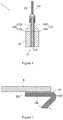
- Figure 1 shows an exemplary electrode plate in the existing technologies.
- a current collector 11 of a multilayer structure is selected for some electrode plates 1.
- the current collector 11 includes an insulating layer 111, a first conductive layer 112 and a second conductive layer 113, where the first layer 112 and the second conductive layer 113 are respectively provided to two surfaces of the insulating layer 111.
- the first conductive layer 112 includes a first body section 1121 covered by an active material layer 12 and a first protruding section 1122 protruding to an outside of the active material layer 12.
- the second conductive layer 113 includes a second body section 1131 covered by the active material layer 12 and a second protruding section 1132 protruding to an outside of the active material layer 12.
- the first protruding section 1122, the second protruding section 1132, and a section of the insulating layer 111 between the first protruding section 1122 and the second protruding section 1132 form an electric guiding section P. Since the first conductive layer 112 and the second conductive layer 113 are separated by the insulating layer 111, current cannot be transmitted between the first conductive layer 112 and the second conductive layer 113, resulting in poor current passing capacity of the electric guiding section P.
- a first conductive member 131 is usually soldered onto the first conductive layer 112
- a second conductive member 132 is usually soldered onto the second conductive layer 113
- the first conductive member 131 and the second conductive member 132 are both soldered to an adapter sheet 6 fixed to an electrode terminal.
- currents in the first conductive layer 112 and second conductive layer 113 are collected to the electrode terminal.
- both the first conductive member 131 and the second conductive member 132 need to be laminated together and soldered to the adapter sheet 6. This, however, will cause the first conductive member 131 and the second conductive member 132 to take a large amount of space, resulting in a reduced energy density for the secondary battery.
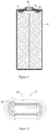
- the secondary battery includes an electrode assembly, a case 2, a top cap 3, an electrode terminal 4 and an adapter sheet 6.
- the electrode assembly includes a positive electrode plate 1A, a negative electrode plate 1B and a separator 5 arranged between the positive electrode plate 1A and the negative electrode plate 1B.
- the positive electrode plate 1A, the separator 5, and the negative electrode plate 1B are sequentially laminated and wound to form a jelly roll-shaped electrode assembly.
- the positive electrode plate 1A, the separator 5, and the negative electrode plate 1B may also be sequentially laminated to form a laminated electrode assembly.
- the case 2 may be of a hexahedron shape or another shape.
- An accommodating cavity is formed inside the case 2 to accommodate the electrode assembly and electrolyte.
- An opening is formed at one end of the case 2, through which the electrode assembly may be placed in the accommodating cavity of the case 2.
- the case 2 may be made of either such conductive metals as aluminum or aluminum alloy or such insulating materials as plastic.
- the top cap 3 is arranged at the case 2, covering the opening of the case 2, so that the electrode assembly is sealed inside the case 2.
- the electrode terminal 4 is arranged at the top cap 3, and an upper end of the electrode terminal 4 protrudes upwards from the top cap 3, while a lower end of the electrode terminal 4 may pass through the top cap 3 and extend into the case 2.
- the adapter sheet 6 is arranged inside the case 2, fixed to the electrode terminal 4. There are two electrode terminals 4 and two adapter sheets 6, and the positive electrode plate 1A connects to one electrode terminal 4 via one adapter sheet 6, while the negative electrode plate 1B connects to the other electrode terminal 4 via the other adapter 6.
- At least one of the positive electrode plate 1A and the negative electrode plate 1B uses an electrode plate 1 described below.
- the electrode plate 1 includes a current collector 11, an active material layer 12 and a conductive structure 13.
- the current collector 11 includes an insulating layer 111, a first conductive layer 112 and a second conductive layer 113.
- the first conductive 112 and the second conductive layer 113 are respectively arranged on two surfaces of the insulating layer 111.
- the first conductive layer 112 has a first body section 1121 and a first protruding section 1122 connected to the first body portion 1121.
- the surface of the first body section 1121 away from the insulating layer 111 is covered by the active material layer 12, while the surface of the first protruding section 1122 away from the insulating layer 111 is not covered by the active material layer 12.
- the second conductive layer 113 has a second body section 1131 and a second protruding section 1132 connected to the second body section 1131.
- the surface of the second body section 1131 away from the insulating layer 111 is covered by the active material layer 12, while the surface of the second protruding section 1132 away from the insulating layer 111 is not covered by the active material layer 12.
- a conductive structure 13 includes a first conductive member 131 connected to the first protruding section 1122 and a second conductive member 132 connected to the second protruding section 1132.
- the second conductive member 132 is bent towards and connected to the first conductive member 131.
- the second conductive member 132 may either directly connect the first conductive member 131, or indirectly connect the first conductive member 131 via the first protruding section 1122.
- the first conductive member 131 extends away from the active material layer 12 beyond the second conductive member 132.
- a part of the first conductive member 131 extends beyond the second conductive member 132 in the direction away from the active material layer 12, the part of the first conductive member 131 beyond the second conductive member 132 is defined as a current collecting section C.
- the first protruding section 1122, the second protruding section 1132, and a section of the insulating layer 111 between the first protruding section 1122 and the second protruding section 1132 form an electric guiding section P.
- the electrode assembly has a plurality of electric guiding sections P and a plurality of conductive structures 13, the plurality of electric guiding sections P are arranged to be laminated.
- the current collecting section C of one conductive structure 13 contacts with the current collecting section C of another conductive structure 13.
- each current collecting section C of the plurality of conductive structures 13 are connected to the adapter sheet 6, and each second conductive member 132 of the plurality of conductive structures 13 is located at a side of the current collecting section C away from the adapter sheet 6.
- the current collecting section C of the plurality of conductive structures 13 may be soldered to the adapter sheet 6 in the first place. Then with reference to Figures 3 and 9 , the second conductive member 132 is flipped to the lower side of the adapter sheet 6 via the bent current collecting section C.
- the first and/or conductive layer has a thickness of 0.1 ⁇ 10um, for example, 0.1um, 1um, 2 um, 3 um, 4 um, 5 um, 6 um, 7 um, 8 um, 9 um, 10 um. In some embodiments, the first and/or conductive layer has a thickness of 0.7-0.9 um, for example, 0.7 um, 0.8 um, 0.9 um.
- the first conductive member 131 and the second conductive member 132 may collect current in the first conductive layer 112 and the second conductive layer 113 to the adapter sheet 6, thereby improving current passing capacity.
- the currents in the first conductive layer 112 and the second conductive layer 113 may be collected to the adapter sheet 6 by simply connecting the current collecting section C of the first conductive member 131 to the adapter sheet 6 without the need for the second conductive member 132 to be connected to the adapter sheet 6. Therefore, the present application may reduce the overall thickness after the adapter sheet 6 and the conductive structure 13 are connected together and the space taken by the conductive structure 13, and improves energy density of the secondary battery, as compared with existing technologies.
- the second conductive member 132 includes a first connecting section 1321 connected to the second protruding section 1132, second connecting section 1323 connected to the first conductive member 131, and a bent section 1322 bent towards the first conductive member 131 relatively to the first connecting section 1321.
- the bent section 1322 is connected between the first connecting section 1321 and the second connecting section 1323.
- the electrode plate 1 can be formed differently, as explained below.
- first metal foils are soldered to the first conductive layer 112 and the second conductive layer 113. Then the two metal foils are bent and connected. Finally, the first protruding section 1122, the second protruding section 1132, the first conductive member 131 and the second conductive member 132 of desired shapes are formed by cutting the first conductive layer 112, the second conductive layer 113 and the two metal foils. At this time, the bent portion 1322 is preferably located on the side of the second protruding section 1132 away from the active material layer 12, so that the bending of the second conductive member 132 may be completed before the cutting process.
- the forming method may simultaneously form at least two first conductive members 131 and second conductive members 132 to facilitate continuous production.
- first conductive layer 112 and the second conductive layer 113 are firstly cut to form a first protruding section 1122 and a second protruding section 1132 of desired shapes. Then the cut first conductive member 131 and the cut second conductive member 132 are respectively soldered to the first protruding section 1122 and the second protruding section 1132. Finally, the second conductive member 132 is folded and connected to the first conductive member 131.
- the bent section 1322 may be located on the side of the electric guiding section P in the length direction X. At this time, the end of the electric guiding section P away from the active material layer 12 may extend beyond the end of the second conductive member 132 away from the active material layer 12.
- the second conductive member 132 does not take additional space in the height direction Z.
- electrode plate 1 of the present disclosure will now be described below.
- Figure 8 shows a first exemplary electrode plate according to some embodiments of the present disclosure.
- the second connecting section 1323 is bent towards the active material layer 12 relatively to the bent section 1322, and the second connecting section 1323 is connected between the first conductive member 131 and the first protruding section 1122.
- the second connecting section 1323 is located on the side of the bent section 1322 closer to the active material layer 12, and the section of the first conductive member 131 beyond the bent section 1322 is the current collecting section C. Accordingly, the length of the current collecting section C may be increased relatively.
- the first conductive member 131, the second connecting section 1323, and the first protruding section 1122 may be integrally soldered together, therefore a first fusion region W1 is formed.
- Insulating cement may be disposed on the surface of the first fusion region W1 and the surface of the first fusion region W1 is away from the insulating layer 111.
- the first connecting section 1321 may also be fixed to the second protruding section 1132 by soldering. It can be understood by the skilled person that in one example after the soldering, particles of the soldering materials may be formed onto the surface of the first fusion region W1 which is away from the insulating layer 111. Due to the insulating cement, the particles can be fixed in the insulating cement, and thus the particles are prevented from moving onto other parts of the electrode plate. Therefore, undesired short circuit caused by the particles can be effectively avoided.
- Figure 10 shows a second exemplary electrode plate according to some embodiments of the present disclosure.
- the second connecting section 1323 is bent towards the active material layer 12 relatively to the bent section 1322, and the second connecting section 1323 is connected between the first conductive member 131 and the first protruding section 1122.
- the conductive structure 13 is an integrally formed piece, and an end of the first conductive member 131 closer to the active material layer 12 is connected to an end of the second connecting section 1323 that is closer to the active material layer 12.
- the strength of the conductive structure 13 can be improved and it is easier to manufacture and assemble the electrode plate.
- the conductive structure 13 may be assembled according to the following steps. First, the conductive structure 13 is soldered to the second protruding section 1132. Then the section of the conductive structure 13 beyond the electric guiding section P is bent onto the first protruding section 1122, and the conductive structure 13 is soldered to the first protruding section 1122. Finally, the conductive structure 13 is bent again to form the first conductive member 131.
- Figure 11 shows a third exemplary electrode plate according to some embodiments of the present disclosure.
- the second connecting section 1323 is bent towards the active material layer 12 relatively to the bent section 1322, and the second connecting portion 1323 is connected between the first conductive member 131 and the first protruding section 1122.
- the conductive structure 13 is integrally formed, and an end of the first conductive member 131 closer to the active material layer 12 is connected to an end of the second connecting portion 1323 closer to the active material layer 12.
- the first conductive member 131, the second connecting portion 1323, and the first protruding section 1122 are integrally soldered together, and the first fusion region W1 can be formed.
- the third exemplary electrode plate can increase the current passing area between the first conductive member 131 and the second connecting section 1323.
- Figure 12 shows a fourth exemplary electrode plate according to some embodiments of the present disclosure.
- the second connecting section 1323 is bent towards the active material layer 12 relatively to the bent section 1322, and the second connecting portion 1323 is connected between the first conductive member 131 and the first protruding section 1122.
- the first conductive member 131 is connected to a section of the first protruding section 1122 between the second connecting section 1323 and the active material layer 12, and the first conductive member 131 is indirectly connected to the second connecting section 1323 via the first protruding section 1122.
- the first conductive member 131 is soldered to the first protruding section 1122 and forms a second fusion region W2, and the second connecting section 1323 is located on a side of the second fusion region W2 away from the active material layer 12.
- an effect of the exemplary electrode plate is to further increase the current passing area between the first conductive member 131 and the second connecting section 1323. This is due to the presence of the second fusion region W2 and the close contact between first conductive member 131 and the second connecting section 1323.
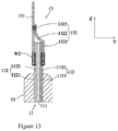
- Figure 13 shows a fifth exemplary electrode plate according to some embodiments of the present disclosure.
- the second connecting section 1323 is connected to an end of the bent section 1322 that is closer to the first conductive member 131, and extends away from the current collector 11.
- the first conductive member 131 and the second conductive member 132 are firstly soldered to the first protruding region 1122 and the second protruding region 1132, respectively.
- the section of the second conductive member 132 beyond the electric guiding section P is bent onto the first conductive member 131.
- the first conductive member 131 and the second conductive member 132 are soldered together.
- the manufacturing process of bending the second conductive member 132 is simple.
- the current in the first conductive layer and the second conductive layer may be collected to the adapter sheet simply by connecting the current collector of the first conductive member to the adapter sheet without connecting the second conductive member to the adapter sheet. Therefore, compared with the existing technologies, the present application may reduce an overall thickness after the adapter sheet and conductive structure are connected together, so that the space taken by a conductive structure is reduced and the energy density of the secondary battery is improved.
Landscapes
- Chemical & Material Sciences (AREA)
- General Chemical & Material Sciences (AREA)
- Chemical Kinetics & Catalysis (AREA)
- Electrochemistry (AREA)
- Engineering & Computer Science (AREA)
- Manufacturing & Machinery (AREA)
- Materials Engineering (AREA)
- Composite Materials (AREA)
- Life Sciences & Earth Sciences (AREA)
- Biophysics (AREA)
- Computer Hardware Design (AREA)
- Connection Of Batteries Or Terminals (AREA)
- Secondary Cells (AREA)
Claims (12)
- Elektrodenplatte (1) für eine Sekundärbatterie, umfassend:eine aktive Materialschicht (12);einen Stromabnehmer (11), umfassend:eine Isolierschicht (111);eine erste leitfähige Schicht (112), umfassend:einen ersten Körperabschnitt (1121), wobei eine Fläche des ersten Körperabschnitts (1121), die von der Isolierschicht (111) entfernt ist, von der aktiven Materialschicht (12) abgedeckt ist;einen ersten hervorragenden Abschnitt (1122), der derart angeordnet ist, dass er an den ersten Körperabschnitt (1121) anschließt, wobei eine Fläche des ersten hervorragenden Abschnitts (1122), die von der Isolierschicht (111) entfernt ist, nicht von der aktiven Materialschicht (12) abgedeckt ist;eine zweite leitfähige Schicht (113), umfassend einen zweiten Körperabschnitt (1131), wobei eine Fläche des zweiten Körperabschnitts (1131), die von der Isolierschicht (111) entfernt ist, von der aktiven Materialschicht (12) abgedeckt ist; einen zweiten hervorragenden Abschnitt (1132), der derart angeordnet ist, dass er an den zweiten Körperabschnitt (1131) anschließt, wobei eine Fläche des zweiten hervorragenden Abschnitts (1132), die von der Isolierschicht (111) entfernt ist, nicht von der aktiven Materialschicht (12) abgedeckt ist;wobei die erste leitfähige Schicht (112) und die zweite leitfähige Schicht (113) jeweils auf zwei Flächen der Isolierschicht (111) angeordnet sind;eine leitfähige Struktur (13), umfassend:ein erstes leitfähiges Bauteil (131), das derart angeordnet ist, dass es an den ersten hervorragenden Abschnitt (1122) anschließt;ein zweites leitfähiges Bauteil (132), das derart angeordnet ist, dass es an den zweiten hervorragenden Abschnitt (1132) anschließt;wobei das zweite leitfähige Bauteil (132) zu dem ersten leitfähigen Bauteil (131) gebogen ist und an das erste leitfähige Bauteil (131) anschließt,und wobei sich das erste leitfähige Bauteil (131) von der aktiven Materialschicht (12) weg erstreckt undüber das zweite leitfähige Bauteil (132) hinaus geht.
- Elektrodenplatte (1) nach Anspruch 1, wobei das zweite leitfähige Bauteil (132) umfasst:einen ersten Anschlussabschnitt (1321), der derart angeordnet ist, dass er an den zweiten hervorragenden Abschnitt (1132) anschließt;einen gebogenen Abschnitt (1322), der in Bezug auf den ersten Anschlussabschnitt (1321) zu dem ersten leitfähigen Bauteil (131) gebogen ist; undeinen zweiten Anschlussabschnitt (1323), der derart angeordnet ist, dass er an das erste leitfähige Bauteil (131) anschließt;wobei der gebogene Abschnitt (1322) den ersten Anschlussabschnitt (1321) mit dem zweiten Anschlussabschnitt (1323) verbindet.
- Elektrodenplatte (1) nach Anspruch 2, wobei sich der gebogene Abschnitt (1322) auf einer Seite des zweiten hervorragenden Abschnitts (1132) befindet, wobei die Seite von der aktiven Materialschicht (12) entfernt ist.
- Elektrodenplatte (1) nach Anspruch 2 oder 3, wobei der zweite Anschlussabschnitt (1323) in Bezug auf den gebogenen Abschnitt (1322) zu der aktiven Materialschicht (12) gebogen ist und das erste leitfähige Bauteil (131) mit dem ersten hervorragenden Abschnitt (1122) verbindet.
- Elektrodenplatte (1) nach einem der Ansprüche 2 bis 4, wobei die leitfähige Struktur (13) einstückig ausgebildet ist und ein Ende des ersten leitfähigen Bauteils (131), das der aktiven Materialschicht (12) näher ist, an ein Ende des zweiten Anschlussabschnitts (1323) anschließt, welches der aktiven Materialschicht (12) näher ist.
- Elektrodenplatte (1) nach einem der Ansprüche 2 bis 4, wobei das erste leitfähige Bauteil (131) an einen Abschnitt des ersten hervorragenden Abschnitts (1122) anschließt, wobei sich der Abschnitt zwischen dem zweiten Anschlussabschnitt (1323) und der aktiven Materialschicht (12) befindet.
- Elektrodenplatte (1) nach Anspruch 2 oder 3, wobei der zweite Anschlussabschnitt (1323) an ein Ende des gebogenen Abschnitts (1322) anschließt, wobei sich das Ende des gebogenen Abschnitts (1322) näher an dem ersten leitfähigen Bauteil (131) befindet und sich von dem Stromabnehmer (11) weg erstreckt.
- Elektrodenplatte (1) nach einem der vorhergehenden Ansprüche, wobei die erste leitfähige Schicht (112) eine Dicke von 0,7∼0,9 µm aufweist.
- Elektrodenplatte (1) nach einem der vorhergehenden Ansprüche, wobei die zweite leitfähige Schicht (113) eine Dicke von 0,7∼0,9 µm aufweist.
- Sekundärbatterie, umfassend eine Elektrodenbaugruppe, welche die Elektrodenplatte (1) nach einem der Ansprüche 1 bis 9 umfasst.
- Sekundärbatterie nach Anspruch 10, wobei der erste hervorragende Abschnitt (1122), der zweite hervorragende Abschnitt (1132) und ein Abschnitt der Isolierschicht (111), die sich zwischen dem ersten hervorragenden Abschnitt (1122) und dem zweiten hervorragenden Abschnitt (1132) befindet, einen Stromführungsabschnitt (P) bilden;
wobei die Elektrodenbaugruppe wenigstens zwei Stromführungsabschnitte (P) und wenigstens zwei leitfähige Strukturen (13) aufweist und die wenigstens zwei Stromführungsabschnitte (P) geschichtet sind;
wobei der Abschnitt des ersten leitfähigen Bauteils (131), der über das zweite leitfähige Bauteil (132) hinausgeht, ein Stromabnahmeabschnitt (C) ist und ein Stromabnahmeabschnitt (C) einer der wenigstens zwei leitfähigen Strukturen (13) einen Stromabnahmeabschnitt (C) einer benachbarten leitfähigen Struktur (13) berührt. - Sekundärbatterie nach Anspruch 11, wobei die Sekundärbatterie ferner eine Elektrodenklemme (4) und eine Adapterschicht (6) aufweist, die derart angeordnet ist, dass sie an die Elektrodenklemme (4) anschließt, wobei jeder Stromabnahmeabschnitt (C) der wenigstens zwei leitfähigen Strukturen (13) mit der Adapterschicht (6) verbunden ist und sich jedes zweite leitfähige Bauteil (132) der wenigstens zwei leitfähigen Strukturen (13) auf einer von der Adapterschicht (6) entfernten Seite des Stromabnahmeabschnitts (C) befindet.
Priority Applications (1)
| Application Number | Priority Date | Filing Date | Title |
|---|---|---|---|
| PL18248114T PL3595044T3 (pl) | 2018-07-13 | 2018-12-28 | Akumulator i płyta elektrodowa |
Applications Claiming Priority (1)
| Application Number | Priority Date | Filing Date | Title |
|---|---|---|---|
| CN201810768859.5A CN108963311B (zh) | 2018-07-13 | 2018-07-13 | 二次电池及其极片 |
Publications (2)
| Publication Number | Publication Date |
|---|---|
| EP3595044A1 EP3595044A1 (de) | 2020-01-15 |
| EP3595044B1 true EP3595044B1 (de) | 2021-07-28 |
Family
ID=64483194
Family Applications (1)
| Application Number | Title | Priority Date | Filing Date |
|---|---|---|---|
| EP18248114.3A Active EP3595044B1 (de) | 2018-07-13 | 2018-12-28 | Sekundärbatterie und elektrodenplatte |
Country Status (5)
| Country | Link |
|---|---|
| US (3) | US20200020952A1 (de) |
| EP (1) | EP3595044B1 (de) |
| CN (2) | CN108963311B (de) |
| HU (1) | HUE056627T2 (de) |
| PL (1) | PL3595044T3 (de) |
Families Citing this family (18)
| Publication number | Priority date | Publication date | Assignee | Title |
|---|---|---|---|---|
| KR102112227B1 (ko) * | 2018-07-27 | 2020-05-18 | 주식회사 유앤에스에너지 | 전극용 집전체 |
| CN210805919U (zh) * | 2019-10-16 | 2020-06-19 | 宁德时代新能源科技股份有限公司 | 二次电池及其电极构件、电池模块和使用二次电池的装置 |
| CN112825381A (zh) * | 2019-11-19 | 2021-05-21 | 深圳市海鸿新能源技术有限公司 | 二次电池的极片及其制备方法、二次电池 |
| WO2021098889A1 (zh) * | 2019-11-19 | 2021-05-27 | 深圳市海鸿新能源技术有限公司 | 二次电池的极片及其制备方法、二次电池 |
| AU2020391409A1 (en) * | 2019-11-27 | 2022-07-21 | Soteria Battery Innovation Group Inc. | Battery with metalized film current collector having low internal resistance |
| CN111509180B (zh) * | 2020-03-26 | 2022-04-12 | 合肥国轩高科动力能源有限公司 | 一种极耳导通的锂电池电芯 |
| CN114583178A (zh) * | 2020-11-30 | 2022-06-03 | 比亚迪股份有限公司 | 一种电池集流体及锂离子电池 |
| CN115117462B (zh) * | 2021-03-18 | 2025-04-22 | 宁德新能源科技有限公司 | 电芯、电池包以及电子设备 |
| CN113795955B (zh) * | 2021-03-30 | 2024-10-22 | 宁德新能源科技有限公司 | 电池及应用所述电池的电子装置 |
| HUE070435T2 (hu) * | 2021-04-22 | 2025-06-28 | Contemporary Amperex Technology Hong Kong Ltd | Elektródszerelvény és gyártási eljárás és hozzávaló gyártórendszer, akkumulátorcella és akkumulátor |
| CN113708018B (zh) * | 2021-09-02 | 2023-10-20 | 北京卫蓝新能源科技有限公司 | 一种复合集流体极耳焊接结构、焊接方法及电池 |
| CN115995562A (zh) * | 2021-10-20 | 2023-04-21 | 华为技术有限公司 | 第一电极片、裸电芯、电池以及电子设备 |
| CN114665101B (zh) * | 2022-03-02 | 2024-07-16 | 东莞新能安科技有限公司 | 电化学装置以及电子装置 |
| CN218867151U (zh) * | 2022-11-14 | 2023-04-14 | 宁德时代新能源科技股份有限公司 | 一种电极构件、电池单体、电池及用电装置 |
| CN118633175A (zh) * | 2023-01-09 | 2024-09-10 | 宁德时代新能源科技股份有限公司 | 电极极片、电极组件、电池单体、电池和用电设备 |
| CN117996369A (zh) * | 2024-02-06 | 2024-05-07 | 宁德新能源科技有限公司 | 二次电池以及电子装置 |
| WO2025245896A1 (zh) * | 2024-05-31 | 2025-12-04 | 宁德时代新能源科技股份有限公司 | 电池单体、电池及用电装置 |
| EP4693627A1 (de) * | 2024-08-06 | 2026-02-11 | Samsung Sdi Co., Ltd. | Sekundärbatterie mit verbindungselement für den anschluss einer elektrodenlasche und verfahren zu ihrer herstellung |
Family Cites Families (31)
| Publication number | Priority date | Publication date | Assignee | Title |
|---|---|---|---|---|
| JPH10255754A (ja) * | 1997-03-12 | 1998-09-25 | Japan Storage Battery Co Ltd | 電池用極板の集電体とリードとの接続構造及び電池 |
| US6849358B2 (en) | 2001-04-06 | 2005-02-01 | Ngk Spark Plug Co., Ltd. | Lithium ion battery |
| KR100544119B1 (ko) * | 2003-06-24 | 2006-01-23 | 삼성에스디아이 주식회사 | 파우치형 리튬 이차 전지 |
| KR100789062B1 (ko) | 2004-09-30 | 2007-12-26 | 스미토모덴키고교가부시키가이샤 | 비수 전해질 전지용 리드선 및 비수 전해질 전지 |
| JP2006236960A (ja) * | 2005-01-28 | 2006-09-07 | Fujikura Ltd | 色素増感太陽電池及びその製造方法 |
| KR100891078B1 (ko) * | 2006-04-03 | 2009-03-30 | 주식회사 엘지화학 | 안전성과 용량이 증가된 리튬 이차전지 |
| KR100846071B1 (ko) * | 2006-07-18 | 2008-07-14 | 주식회사 엘지화학 | 신규한 전극리드-전극 탭 결합부로 이루어진 전극조립체 및이를 포함하고 있는 전기화학 셀 |
| US20090035657A1 (en) * | 2006-10-23 | 2009-02-05 | Buiel Edward R | Electrode for Hybrid Energy Storage Device and Method of Making Same |
| JP5353032B2 (ja) * | 2007-07-11 | 2013-11-27 | 日産自動車株式会社 | 積層型電池 |
| US8734986B2 (en) | 2007-07-11 | 2014-05-27 | Nissan Motor Co., Ltd. | Laminate type battery |
| JP2009187675A (ja) * | 2008-02-01 | 2009-08-20 | Sharp Corp | 積層型二次電池およびその製造方法 |
| US20100178559A1 (en) | 2009-01-14 | 2010-07-15 | Ou Mao | Nickel-copper clad tabs for rechargeable battery electrodes and methods of manufacturing |
| KR20110123462A (ko) * | 2010-05-07 | 2011-11-15 | 에스비리모티브 주식회사 | 이차 전지 |
| KR101127615B1 (ko) | 2010-07-19 | 2012-07-12 | 삼성에스디아이 주식회사 | 배터리 팩 |
| JP5690575B2 (ja) | 2010-12-16 | 2015-03-25 | シャープ株式会社 | 非水系二次電池 |
| JP5937969B2 (ja) * | 2011-01-07 | 2016-06-22 | シャープ株式会社 | 非水系二次電池 |
| JP5784928B2 (ja) * | 2011-03-03 | 2015-09-24 | シャープ株式会社 | 非水系二次電池 |
| JP2013008564A (ja) * | 2011-06-24 | 2013-01-10 | Sharp Corp | 非水系二次電池およびその製造方法 |
| JP2013012405A (ja) * | 2011-06-29 | 2013-01-17 | Sharp Corp | 非水系二次電池 |
| JP2013016321A (ja) * | 2011-07-01 | 2013-01-24 | Sharp Corp | 集電体および非水系二次電池 |
| KR20130138371A (ko) * | 2012-06-11 | 2013-12-19 | 주식회사 엘지화학 | 신규한 구조의 전극조립체 및 이를 포함하고 있는 전기화학 셀 |
| JP6065010B2 (ja) * | 2012-08-28 | 2017-01-25 | 株式会社豊田自動織機 | 蓄電装置 |
| EP2892103B1 (de) * | 2012-08-29 | 2018-02-14 | Showa Denko K.K. | Stromspeichervorrichtung und herstellungsverfahren dafür |
| JP2014053230A (ja) | 2012-09-10 | 2014-03-20 | Sumitomo Electric Ind Ltd | 非水電解質蓄電デバイス用のリード部材及びその製造方法 |
| EP2939306B1 (de) * | 2012-12-25 | 2020-11-11 | Byd Company Limited | Batterie |
| WO2014101479A1 (en) | 2012-12-25 | 2014-07-03 | Shenzhen Byd Auto R&D Company Limited | Battery |
| KR102465163B1 (ko) * | 2016-06-22 | 2022-11-08 | 가부시키가이샤 한도오따이 에네루기 켄큐쇼 | 전지, 및 전지의 제작 방법 |
| US11539050B2 (en) * | 2017-01-12 | 2022-12-27 | Contemporary Amperex Technology Co., Limited | Current collector, electrode plate and battery containing the same, and application thereof |
| CN110800130B (zh) * | 2017-06-23 | 2022-06-14 | 株式会社丰田自动织机 | 蓄电装置 |
| US11201318B2 (en) * | 2017-09-15 | 2021-12-14 | Honda Motor Co., Ltd. | Method for battery tab attachment to a self-standing electrode |
| CN207542313U (zh) * | 2017-11-22 | 2018-06-26 | 宁德时代新能源科技股份有限公司 | 电极构件、电极组件和充电电池 |
-
2018
- 2018-07-13 CN CN201810768859.5A patent/CN108963311B/zh active Active
- 2018-07-13 CN CN202010157355.7A patent/CN111244388B/zh active Active
- 2018-12-27 US US16/233,296 patent/US20200020952A1/en not_active Abandoned
- 2018-12-28 EP EP18248114.3A patent/EP3595044B1/de active Active
- 2018-12-28 HU HUE18248114A patent/HUE056627T2/hu unknown
- 2018-12-28 PL PL18248114T patent/PL3595044T3/pl unknown
-
2023
- 2023-11-23 US US18/518,597 patent/US12463222B2/en active Active
- 2023-11-24 US US18/518,604 patent/US20240088396A1/en active Pending
Also Published As
| Publication number | Publication date |
|---|---|
| EP3595044A1 (de) | 2020-01-15 |
| CN108963311A (zh) | 2018-12-07 |
| CN111244388A (zh) | 2020-06-05 |
| US20200020952A1 (en) | 2020-01-16 |
| HUE056627T2 (hu) | 2022-02-28 |
| US20240088395A1 (en) | 2024-03-14 |
| US20240088396A1 (en) | 2024-03-14 |
| PL3595044T3 (pl) | 2021-12-27 |
| US12463222B2 (en) | 2025-11-04 |
| CN108963311B (zh) | 2020-04-07 |
| CN111244388B (zh) | 2022-02-25 |
Similar Documents
| Publication | Publication Date | Title |
|---|---|---|
| EP3595044B1 (de) | Sekundärbatterie und elektrodenplatte | |
| US11631862B2 (en) | Electrode plate of a secondary battery and a secondary battery | |
| EP3588620B1 (de) | Sekundärbatterie und elektrodenplatte | |
| CN111106300B (zh) | 电池单元及电池模组 | |
| US7326261B2 (en) | Surface-mount capacitor and method of producing the same | |
| EP3633766B1 (de) | Elektrodenelement, elektrodenanordnung und sekundärbatterie | |
| KR20090132494A (ko) | 전극탭 및 이를 포함하는 리튬 이차전지 | |
| JP3252846B2 (ja) | 非水電解液二次電池およびその製造方法 | |
| CN108736054B (zh) | 层叠型电池 | |
| KR102327940B1 (ko) | 적층 금속박의 제조 방법 | |
| US20080232027A1 (en) | Solid electrolytic capacitor | |
| CN113097661A (zh) | 电池 | |
| US6979514B2 (en) | Collector used for an alkali storage battery | |
| JP5229440B2 (ja) | 電気化学デバイス | |
| US11342618B2 (en) | Secondary battery, method of manufacturing the same, and method of manufacturing conductive member for the same | |
| JP4841076B2 (ja) | 密閉型電池 | |
| JP2003243257A (ja) | 固体電解コンデンサ | |
| JP4169495B2 (ja) | 溶接封口電池 | |
| JP4793938B2 (ja) | 積層型コンデンサの製造方法 | |
| JP2010198842A (ja) | 金属プレス成形体及びこれを用いた電池 | |
| JP2010010350A (ja) | 固体電解コンデンサおよびその製造方法 | |
| KR20250094329A (ko) | 이차전지 | |
| WO2024202139A1 (ja) | 電池および電池の製造方法 | |
| JPH06203837A (ja) | 薄形電池 |
Legal Events
| Date | Code | Title | Description |
|---|---|---|---|
| PUAI | Public reference made under article 153(3) epc to a published international application that has entered the european phase |
Free format text: ORIGINAL CODE: 0009012 |
|
| STAA | Information on the status of an ep patent application or granted ep patent |
Free format text: STATUS: REQUEST FOR EXAMINATION WAS MADE |
|
| 17P | Request for examination filed |
Effective date: 20190605 |
|
| AK | Designated contracting states |
Kind code of ref document: A1 Designated state(s): AL AT BE BG CH CY CZ DE DK EE ES FI FR GB GR HR HU IE IS IT LI LT LU LV MC MK MT NL NO PL PT RO RS SE SI SK SM TR |
|
| AX | Request for extension of the european patent |
Extension state: BA ME |
|
| REG | Reference to a national code |
Ref country code: DE Ref legal event code: R079 Ref document number: 602018020748 Country of ref document: DE Free format text: PREVIOUS MAIN CLASS: H01M0002260000 Ipc: H01M0004640000 |
|
| GRAP | Despatch of communication of intention to grant a patent |
Free format text: ORIGINAL CODE: EPIDOSNIGR1 |
|
| STAA | Information on the status of an ep patent application or granted ep patent |
Free format text: STATUS: GRANT OF PATENT IS INTENDED |
|
| RIC1 | Information provided on ipc code assigned before grant |
Ipc: H01M 4/64 20060101AFI20210311BHEP Ipc: H01M 4/70 20060101ALI20210311BHEP Ipc: H01M 50/531 20210101ALI20210311BHEP Ipc: H01M 50/116 20210101ALI20210311BHEP Ipc: H01M 50/247 20210101ALI20210311BHEP |
|
| INTG | Intention to grant announced |
Effective date: 20210401 |
|
| GRAS | Grant fee paid |
Free format text: ORIGINAL CODE: EPIDOSNIGR3 |
|
| GRAA | (expected) grant |
Free format text: ORIGINAL CODE: 0009210 |
|
| STAA | Information on the status of an ep patent application or granted ep patent |
Free format text: STATUS: THE PATENT HAS BEEN GRANTED |
|
| AK | Designated contracting states |
Kind code of ref document: B1 Designated state(s): AL AT BE BG CH CY CZ DE DK EE ES FI FR GB GR HR HU IE IS IT LI LT LU LV MC MK MT NL NO PL PT RO RS SE SI SK SM TR |
|
| REG | Reference to a national code |
Ref country code: GB Ref legal event code: FG4D |
|
| REG | Reference to a national code |
Ref country code: CH Ref legal event code: EP |
|
| REG | Reference to a national code |
Ref country code: AT Ref legal event code: REF Ref document number: 1415510 Country of ref document: AT Kind code of ref document: T Effective date: 20210815 |
|
| REG | Reference to a national code |
Ref country code: IE Ref legal event code: FG4D |
|
| REG | Reference to a national code |
Ref country code: DE Ref legal event code: R096 Ref document number: 602018020748 Country of ref document: DE |
|
| REG | Reference to a national code |
Ref country code: SE Ref legal event code: TRGR |
|
| REG | Reference to a national code |
Ref country code: LT Ref legal event code: MG9D |
|
| REG | Reference to a national code |
Ref country code: NL Ref legal event code: MP Effective date: 20210728 |
|
| REG | Reference to a national code |
Ref country code: AT Ref legal event code: MK05 Ref document number: 1415510 Country of ref document: AT Kind code of ref document: T Effective date: 20210728 |
|
| PG25 | Lapsed in a contracting state [announced via postgrant information from national office to epo] |
Ref country code: PT Free format text: LAPSE BECAUSE OF FAILURE TO SUBMIT A TRANSLATION OF THE DESCRIPTION OR TO PAY THE FEE WITHIN THE PRESCRIBED TIME-LIMIT Effective date: 20211129 Ref country code: NL Free format text: LAPSE BECAUSE OF FAILURE TO SUBMIT A TRANSLATION OF THE DESCRIPTION OR TO PAY THE FEE WITHIN THE PRESCRIBED TIME-LIMIT Effective date: 20210728 Ref country code: NO Free format text: LAPSE BECAUSE OF FAILURE TO SUBMIT A TRANSLATION OF THE DESCRIPTION OR TO PAY THE FEE WITHIN THE PRESCRIBED TIME-LIMIT Effective date: 20211028 Ref country code: AT Free format text: LAPSE BECAUSE OF FAILURE TO SUBMIT A TRANSLATION OF THE DESCRIPTION OR TO PAY THE FEE WITHIN THE PRESCRIBED TIME-LIMIT Effective date: 20210728 Ref country code: BG Free format text: LAPSE BECAUSE OF FAILURE TO SUBMIT A TRANSLATION OF THE DESCRIPTION OR TO PAY THE FEE WITHIN THE PRESCRIBED TIME-LIMIT Effective date: 20211028 Ref country code: LT Free format text: LAPSE BECAUSE OF FAILURE TO SUBMIT A TRANSLATION OF THE DESCRIPTION OR TO PAY THE FEE WITHIN THE PRESCRIBED TIME-LIMIT Effective date: 20210728 Ref country code: RS Free format text: LAPSE BECAUSE OF FAILURE TO SUBMIT A TRANSLATION OF THE DESCRIPTION OR TO PAY THE FEE WITHIN THE PRESCRIBED TIME-LIMIT Effective date: 20210728 Ref country code: HR Free format text: LAPSE BECAUSE OF FAILURE TO SUBMIT A TRANSLATION OF THE DESCRIPTION OR TO PAY THE FEE WITHIN THE PRESCRIBED TIME-LIMIT Effective date: 20210728 Ref country code: FI Free format text: LAPSE BECAUSE OF FAILURE TO SUBMIT A TRANSLATION OF THE DESCRIPTION OR TO PAY THE FEE WITHIN THE PRESCRIBED TIME-LIMIT Effective date: 20210728 Ref country code: ES Free format text: LAPSE BECAUSE OF FAILURE TO SUBMIT A TRANSLATION OF THE DESCRIPTION OR TO PAY THE FEE WITHIN THE PRESCRIBED TIME-LIMIT Effective date: 20210728 |
|
| PG25 | Lapsed in a contracting state [announced via postgrant information from national office to epo] |
Ref country code: LV Free format text: LAPSE BECAUSE OF FAILURE TO SUBMIT A TRANSLATION OF THE DESCRIPTION OR TO PAY THE FEE WITHIN THE PRESCRIBED TIME-LIMIT Effective date: 20210728 Ref country code: GR Free format text: LAPSE BECAUSE OF FAILURE TO SUBMIT A TRANSLATION OF THE DESCRIPTION OR TO PAY THE FEE WITHIN THE PRESCRIBED TIME-LIMIT Effective date: 20211029 |
|
| REG | Reference to a national code |
Ref country code: HU Ref legal event code: AG4A Ref document number: E056627 Country of ref document: HU |
|
| PG25 | Lapsed in a contracting state [announced via postgrant information from national office to epo] |
Ref country code: DK Free format text: LAPSE BECAUSE OF FAILURE TO SUBMIT A TRANSLATION OF THE DESCRIPTION OR TO PAY THE FEE WITHIN THE PRESCRIBED TIME-LIMIT Effective date: 20210728 |
|
| REG | Reference to a national code |
Ref country code: DE Ref legal event code: R097 Ref document number: 602018020748 Country of ref document: DE |
|
| PG25 | Lapsed in a contracting state [announced via postgrant information from national office to epo] |
Ref country code: SM Free format text: LAPSE BECAUSE OF FAILURE TO SUBMIT A TRANSLATION OF THE DESCRIPTION OR TO PAY THE FEE WITHIN THE PRESCRIBED TIME-LIMIT Effective date: 20210728 Ref country code: SK Free format text: LAPSE BECAUSE OF FAILURE TO SUBMIT A TRANSLATION OF THE DESCRIPTION OR TO PAY THE FEE WITHIN THE PRESCRIBED TIME-LIMIT Effective date: 20210728 Ref country code: RO Free format text: LAPSE BECAUSE OF FAILURE TO SUBMIT A TRANSLATION OF THE DESCRIPTION OR TO PAY THE FEE WITHIN THE PRESCRIBED TIME-LIMIT Effective date: 20210728 Ref country code: EE Free format text: LAPSE BECAUSE OF FAILURE TO SUBMIT A TRANSLATION OF THE DESCRIPTION OR TO PAY THE FEE WITHIN THE PRESCRIBED TIME-LIMIT Effective date: 20210728 Ref country code: CZ Free format text: LAPSE BECAUSE OF FAILURE TO SUBMIT A TRANSLATION OF THE DESCRIPTION OR TO PAY THE FEE WITHIN THE PRESCRIBED TIME-LIMIT Effective date: 20210728 Ref country code: AL Free format text: LAPSE BECAUSE OF FAILURE TO SUBMIT A TRANSLATION OF THE DESCRIPTION OR TO PAY THE FEE WITHIN THE PRESCRIBED TIME-LIMIT Effective date: 20210728 |
|
| PLBE | No opposition filed within time limit |
Free format text: ORIGINAL CODE: 0009261 |
|
| STAA | Information on the status of an ep patent application or granted ep patent |
Free format text: STATUS: NO OPPOSITION FILED WITHIN TIME LIMIT |
|
| 26N | No opposition filed |
Effective date: 20220429 |
|
| PG25 | Lapsed in a contracting state [announced via postgrant information from national office to epo] |
Ref country code: MC Free format text: LAPSE BECAUSE OF FAILURE TO SUBMIT A TRANSLATION OF THE DESCRIPTION OR TO PAY THE FEE WITHIN THE PRESCRIBED TIME-LIMIT Effective date: 20210728 |
|
| REG | Reference to a national code |
Ref country code: CH Ref legal event code: PL |
|
| PG25 | Lapsed in a contracting state [announced via postgrant information from national office to epo] |
Ref country code: LU Free format text: LAPSE BECAUSE OF NON-PAYMENT OF DUE FEES Effective date: 20211228 Ref country code: IE Free format text: LAPSE BECAUSE OF NON-PAYMENT OF DUE FEES Effective date: 20211228 |
|
| PG25 | Lapsed in a contracting state [announced via postgrant information from national office to epo] |
Ref country code: LI Free format text: LAPSE BECAUSE OF NON-PAYMENT OF DUE FEES Effective date: 20211231 Ref country code: CH Free format text: LAPSE BECAUSE OF NON-PAYMENT OF DUE FEES Effective date: 20211231 |
|
| P01 | Opt-out of the competence of the unified patent court (upc) registered |
Effective date: 20230516 |
|
| PG25 | Lapsed in a contracting state [announced via postgrant information from national office to epo] |
Ref country code: CY Free format text: LAPSE BECAUSE OF FAILURE TO SUBMIT A TRANSLATION OF THE DESCRIPTION OR TO PAY THE FEE WITHIN THE PRESCRIBED TIME-LIMIT Effective date: 20210728 |
|
| PG25 | Lapsed in a contracting state [announced via postgrant information from national office to epo] |
Ref country code: MK Free format text: LAPSE BECAUSE OF FAILURE TO SUBMIT A TRANSLATION OF THE DESCRIPTION OR TO PAY THE FEE WITHIN THE PRESCRIBED TIME-LIMIT Effective date: 20210728 |
|
| PG25 | Lapsed in a contracting state [announced via postgrant information from national office to epo] |
Ref country code: TR Free format text: LAPSE BECAUSE OF FAILURE TO SUBMIT A TRANSLATION OF THE DESCRIPTION OR TO PAY THE FEE WITHIN THE PRESCRIBED TIME-LIMIT Effective date: 20210728 |
|
| REG | Reference to a national code |
Ref country code: DE Ref legal event code: R081 Ref document number: 602018020748 Country of ref document: DE Owner name: CONTEMPORARY AMPEREX TECHNOLOGY (HONG KONG) LI, HK Free format text: FORMER OWNER: CONTEMPORARY AMPEREX TECHNOLOGY CO., LTD., NINGDE CITY, FUJIAN, CN |
|
| REG | Reference to a national code |
Ref country code: GB Ref legal event code: 732E Free format text: REGISTERED BETWEEN 20240815 AND 20240821 |
|
| REG | Reference to a national code |
Ref country code: HU Ref legal event code: GB9C Owner name: CONTEMPORARY AMPEREX TECHNOLOGY (HONG KONG) LIMITED, HK Free format text: FORMER OWNER(S): CONTEMPORARY AMPEREX TECHNOLOGY CO., LIMITED, CN Ref country code: HU Ref legal event code: FH1C Free format text: FORMER REPRESENTATIVE(S): SBGK SZABADALMI UEGYVIVOEI IRODA, HU Representative=s name: DANUBIA SZABADALMI ES JOGI IRODA KFT., HU |
|
| PG25 | Lapsed in a contracting state [announced via postgrant information from national office to epo] |
Ref country code: MT Free format text: LAPSE BECAUSE OF FAILURE TO SUBMIT A TRANSLATION OF THE DESCRIPTION OR TO PAY THE FEE WITHIN THE PRESCRIBED TIME-LIMIT Effective date: 20210728 |
|
| REG | Reference to a national code |
Ref country code: BE Ref legal event code: PD Owner name: CONTEMPORARY AMPEREX TECHNOLOGY (HONG KONG) LIMITED; CN Free format text: DETAILS ASSIGNMENT: CHANGE OF OWNER(S), ASSIGNMENT; FORMER OWNER NAME: CONTEMPORARY AMPEREX TECHNOLOGY CO., LIMITED Effective date: 20240807 |
|
| PGFP | Annual fee paid to national office [announced via postgrant information from national office to epo] |
Ref country code: DE Payment date: 20250930 Year of fee payment: 8 |
|
| PGFP | Annual fee paid to national office [announced via postgrant information from national office to epo] |
Ref country code: GB Payment date: 20251001 Year of fee payment: 8 |
|
| PGFP | Annual fee paid to national office [announced via postgrant information from national office to epo] |
Ref country code: IT Payment date: 20251121 Year of fee payment: 8 |
|
| PGFP | Annual fee paid to national office [announced via postgrant information from national office to epo] |
Ref country code: HU Payment date: 20251127 Year of fee payment: 8 Ref country code: FR Payment date: 20251110 Year of fee payment: 8 |
|
| PGFP | Annual fee paid to national office [announced via postgrant information from national office to epo] |
Ref country code: BE Payment date: 20251003 Year of fee payment: 8 |
|
| PGFP | Annual fee paid to national office [announced via postgrant information from national office to epo] |
Ref country code: SE Payment date: 20251001 Year of fee payment: 8 |
|
| PGFP | Annual fee paid to national office [announced via postgrant information from national office to epo] |
Ref country code: PL Payment date: 20251014 Year of fee payment: 8 |