EP3588585B1 - P-type perc double-sided solar cell, assembly thereof, system thereof and preparation method therefor - Google Patents
P-type perc double-sided solar cell, assembly thereof, system thereof and preparation method therefor Download PDFInfo
- Publication number
- EP3588585B1 EP3588585B1 EP18760676.9A EP18760676A EP3588585B1 EP 3588585 B1 EP3588585 B1 EP 3588585B1 EP 18760676 A EP18760676 A EP 18760676A EP 3588585 B1 EP3588585 B1 EP 3588585B1
- Authority
- EP
- European Patent Office
- Prior art keywords
- laser grooving
- silicon wafer
- solar cell
- aluminum grid
- perc solar
- Prior art date
- Legal status (The legal status is an assumption and is not a legal conclusion. Google has not performed a legal analysis and makes no representation as to the accuracy of the status listed.)
- Active
Links
Images

Classifications
-
- H—ELECTRICITY
- H10—SEMICONDUCTOR DEVICES; ELECTRIC SOLID-STATE DEVICES NOT OTHERWISE PROVIDED FOR
- H10F—INORGANIC SEMICONDUCTOR DEVICES SENSITIVE TO INFRARED RADIATION, LIGHT, ELECTROMAGNETIC RADIATION OF SHORTER WAVELENGTH OR CORPUSCULAR RADIATION
- H10F10/00—Individual photovoltaic cells, e.g. solar cells
- H10F10/10—Individual photovoltaic cells, e.g. solar cells having potential barriers
- H10F10/14—Photovoltaic cells having only PN homojunction potential barriers
-
- H—ELECTRICITY
- H10—SEMICONDUCTOR DEVICES; ELECTRIC SOLID-STATE DEVICES NOT OTHERWISE PROVIDED FOR
- H10F—INORGANIC SEMICONDUCTOR DEVICES SENSITIVE TO INFRARED RADIATION, LIGHT, ELECTROMAGNETIC RADIATION OF SHORTER WAVELENGTH OR CORPUSCULAR RADIATION
- H10F10/00—Individual photovoltaic cells, e.g. solar cells
- H10F10/10—Individual photovoltaic cells, e.g. solar cells having potential barriers
- H10F10/14—Photovoltaic cells having only PN homojunction potential barriers
- H10F10/148—Double-emitter photovoltaic cells, e.g. bifacial photovoltaic cells
-
- H—ELECTRICITY
- H10—SEMICONDUCTOR DEVICES; ELECTRIC SOLID-STATE DEVICES NOT OTHERWISE PROVIDED FOR
- H10F—INORGANIC SEMICONDUCTOR DEVICES SENSITIVE TO INFRARED RADIATION, LIGHT, ELECTROMAGNETIC RADIATION OF SHORTER WAVELENGTH OR CORPUSCULAR RADIATION
- H10F19/00—Integrated devices, or assemblies of multiple devices, comprising at least one photovoltaic cell covered by group H10F10/00, e.g. photovoltaic modules
- H10F19/10—Integrated devices, or assemblies of multiple devices, comprising at least one photovoltaic cell covered by group H10F10/00, e.g. photovoltaic modules comprising photovoltaic cells in arrays in a single semiconductor substrate, the photovoltaic cells having vertical junctions or V-groove junctions
-
- H—ELECTRICITY
- H10—SEMICONDUCTOR DEVICES; ELECTRIC SOLID-STATE DEVICES NOT OTHERWISE PROVIDED FOR
- H10F—INORGANIC SEMICONDUCTOR DEVICES SENSITIVE TO INFRARED RADIATION, LIGHT, ELECTROMAGNETIC RADIATION OF SHORTER WAVELENGTH OR CORPUSCULAR RADIATION
- H10F71/00—Manufacture or treatment of devices covered by this subclass
- H10F71/121—The active layers comprising only Group IV materials
-
- H—ELECTRICITY
- H10—SEMICONDUCTOR DEVICES; ELECTRIC SOLID-STATE DEVICES NOT OTHERWISE PROVIDED FOR
- H10F—INORGANIC SEMICONDUCTOR DEVICES SENSITIVE TO INFRARED RADIATION, LIGHT, ELECTROMAGNETIC RADIATION OF SHORTER WAVELENGTH OR CORPUSCULAR RADIATION
- H10F71/00—Manufacture or treatment of devices covered by this subclass
- H10F71/128—Annealing
-
- H—ELECTRICITY
- H10—SEMICONDUCTOR DEVICES; ELECTRIC SOLID-STATE DEVICES NOT OTHERWISE PROVIDED FOR
- H10F—INORGANIC SEMICONDUCTOR DEVICES SENSITIVE TO INFRARED RADIATION, LIGHT, ELECTROMAGNETIC RADIATION OF SHORTER WAVELENGTH OR CORPUSCULAR RADIATION
- H10F71/00—Manufacture or treatment of devices covered by this subclass
- H10F71/129—Passivating
-
- H—ELECTRICITY
- H10—SEMICONDUCTOR DEVICES; ELECTRIC SOLID-STATE DEVICES NOT OTHERWISE PROVIDED FOR
- H10F—INORGANIC SEMICONDUCTOR DEVICES SENSITIVE TO INFRARED RADIATION, LIGHT, ELECTROMAGNETIC RADIATION OF SHORTER WAVELENGTH OR CORPUSCULAR RADIATION
- H10F77/00—Constructional details of devices covered by this subclass
- H10F77/20—Electrodes
- H10F77/206—Electrodes for devices having potential barriers
- H10F77/211—Electrodes for devices having potential barriers for photovoltaic cells
- H10F77/215—Geometries of grid contacts
-
- H—ELECTRICITY
- H10—SEMICONDUCTOR DEVICES; ELECTRIC SOLID-STATE DEVICES NOT OTHERWISE PROVIDED FOR
- H10F—INORGANIC SEMICONDUCTOR DEVICES SENSITIVE TO INFRARED RADIATION, LIGHT, ELECTROMAGNETIC RADIATION OF SHORTER WAVELENGTH OR CORPUSCULAR RADIATION
- H10F77/00—Constructional details of devices covered by this subclass
- H10F77/20—Electrodes
- H10F77/206—Electrodes for devices having potential barriers
- H10F77/211—Electrodes for devices having potential barriers for photovoltaic cells
- H10F77/219—Arrangements for electrodes of back-contact photovoltaic cells
-
- H—ELECTRICITY
- H10—SEMICONDUCTOR DEVICES; ELECTRIC SOLID-STATE DEVICES NOT OTHERWISE PROVIDED FOR
- H10W—GENERIC PACKAGES, INTERCONNECTIONS, CONNECTORS OR OTHER CONSTRUCTIONAL DETAILS OF DEVICES COVERED BY CLASS H10
- H10W10/00—Isolation regions in semiconductor bodies between components of integrated devices
- H10W10/01—Manufacture or treatment
-
- Y—GENERAL TAGGING OF NEW TECHNOLOGICAL DEVELOPMENTS; GENERAL TAGGING OF CROSS-SECTIONAL TECHNOLOGIES SPANNING OVER SEVERAL SECTIONS OF THE IPC; TECHNICAL SUBJECTS COVERED BY FORMER USPC CROSS-REFERENCE ART COLLECTIONS [XRACs] AND DIGESTS
- Y02—TECHNOLOGIES OR APPLICATIONS FOR MITIGATION OR ADAPTATION AGAINST CLIMATE CHANGE
- Y02E—REDUCTION OF GREENHOUSE GAS [GHG] EMISSIONS, RELATED TO ENERGY GENERATION, TRANSMISSION OR DISTRIBUTION
- Y02E10/00—Energy generation through renewable energy sources
- Y02E10/50—Photovoltaic [PV] energy
-
- Y—GENERAL TAGGING OF NEW TECHNOLOGICAL DEVELOPMENTS; GENERAL TAGGING OF CROSS-SECTIONAL TECHNOLOGIES SPANNING OVER SEVERAL SECTIONS OF THE IPC; TECHNICAL SUBJECTS COVERED BY FORMER USPC CROSS-REFERENCE ART COLLECTIONS [XRACs] AND DIGESTS
- Y02—TECHNOLOGIES OR APPLICATIONS FOR MITIGATION OR ADAPTATION AGAINST CLIMATE CHANGE
- Y02E—REDUCTION OF GREENHOUSE GAS [GHG] EMISSIONS, RELATED TO ENERGY GENERATION, TRANSMISSION OR DISTRIBUTION
- Y02E10/00—Energy generation through renewable energy sources
- Y02E10/50—Photovoltaic [PV] energy
- Y02E10/547—Monocrystalline silicon PV cells
-
- Y—GENERAL TAGGING OF NEW TECHNOLOGICAL DEVELOPMENTS; GENERAL TAGGING OF CROSS-SECTIONAL TECHNOLOGIES SPANNING OVER SEVERAL SECTIONS OF THE IPC; TECHNICAL SUBJECTS COVERED BY FORMER USPC CROSS-REFERENCE ART COLLECTIONS [XRACs] AND DIGESTS
- Y02—TECHNOLOGIES OR APPLICATIONS FOR MITIGATION OR ADAPTATION AGAINST CLIMATE CHANGE
- Y02P—CLIMATE CHANGE MITIGATION TECHNOLOGIES IN THE PRODUCTION OR PROCESSING OF GOODS
- Y02P70/00—Climate change mitigation technologies in the production process for final industrial or consumer products
- Y02P70/50—Manufacturing or production processes characterised by the final manufactured product
Definitions
- the present invention relates to the field of solar cells, and in particular to a bifacial P-type PERC solar cell, a method of preparing the bifacial P-type PERC solar cell, a solar cell module that employs the bifacial P-type PERC solar cell, and a solar system that employs the bifacial P-type PERC solar cell.
- a crystalline silicon solar cell is a device that effectively absorbs solar radiation energy and converts light energy into electrical energy through the photovoltaic effect.
- sunlight reaches the p-n junction of a semiconductor, new electron-hole pairs are generated.
- the holes flow from the N zone to the P zone, and the electrons flow from the P zone to the N zone, generating current upon switching on a circuit.
- surface passivation is basically only performed at the front surface, which involves depositing a layer of silicon nitride on the front surface of the silicon wafer via PECVD to reduce the recombination rate of the minority carriers at the front surface.
- the open-circuit voltage and short-circuit current of the crystalline silicon cell can be greatly increased, which leads to an increase of the photoelectric conversion efficiency of the crystalline silicon solar cell.
- passivation is not provided at the rear surface of the silicon wafer, the increase in photoelectric conversion efficiency is still limited.
- the structure of an existing bifacial solar cell is as follows: the substrate is an N-type silicon wafer; when photons from the sun reach the rear surface of the cell, the carriers generated in the N-type silicon wafer pass through the silicon wafer, which has a thickness of about 200 ⁇ m; as in an N-type silicon wafer, the minority carriers have a long lifetime and carrier recombination rate is low, some carriers are able to reach the p-n junction at the front surface; the front surface of the solar cell is the main light-receiving surface, and its conversion efficiency accounts for a high proportion of the conversion efficiency of the whole cell; as a result of overall actions at both the front surface and the rear surface, the conversion efficiency of the cell is significantly increased.
- the industry has been researching rear-surface passivation techniques for PERC solar cells.
- Mainstream manufacturers in the industry are mainly developing monofacial PERC solar cells.
- the present invention combines a highly efficient PERC cell and a bifacial cell to develop a bifacial PERC solar cell that has overall higher photoelectric conversion efficiency.
- Bifacial PERC solar cells have higher usage values in the practical applications as they have high photoelectric conversion efficiency while they absorb solar energy on both sides to generate more power.
- the present invention aims to provide a bifacial P-type PERC solar cell which is simple to manufacture, low in cost, easy to popularize, and has a high photoelectric conversion efficiency.
- a solar cell array is made of a plurality of bifacial PERC solar cells, respectively formed in a semiconductor body, which are electrically interconnected by way of cell connectors.
- a structured passivation layer is applied on the rear-side surface of the semiconductor body, on which the current collecting rails and contact finger contacting the semiconductor body are provided.
- a respective cell connector extends at least partially along a longitudinal direction of at least one current collecting rail and electrically contacts this on at least one solder contact via a solder joint.
- a lateral width of a current collecting rail is at least partially greater than a lateral width of the cell connector covering this current collecting rail.
- DE 10 2015 104 236 A1 relates to a photovoltaic solar cell, comprising at least one semiconductor layer, at least one electrically insulating insulation layer and at least one metal contacting structure, wherein the insulation layer is arranged between the semiconductor layer and the contacting structure, and the insulation layer has a plurality of contacting recesses at which the contacting structure forms an electrical contact with the semiconductor layer in a contacting region, and wherein a respective doping region is formed in the semiconductor layer at least at the contacting regions by doping the semiconductor layer with a metal, from which metal the contacting structure is at least partially formed.
- DE 10 2014 105 358 A1 relates to a solar cell comprising a substrate with a front-side and a rear-side, wherein at least the front-side receives light; a passivation layer on the rear-side of the substrate; local contact openings, which pass through the passivation layer and partially expose the rear-side of the substrate; and a first rear-side metallization on the passivation layer and in the local contact openings; wherein the plurality of the local contact openings are disposed such that they are completely covered by the first rear-side metallization.
- An objective to be addressed by the present invention is to provide a bifacial P-type PERC solar cell which is simple in structure, low in cost, easy to popularize, and has a high photoelectric conversion efficiency.
- Another objective to be addressed by the present invention is to provide a method of preparing the bifacial P-type PERC solar cell, which is simple in process, low in cost, easy to popularize, and has a high photoelectric conversion efficiency.
- Yet another objective to be addressed by the present invention is to provide a bifacial P-type PERC solar cell module which is simple in structure, low in cost, easy to popularize, and has a high photoelectric conversion efficiency.
- Still another objective to be addressed by the present invention is to provide a bifacial P-type PERC solar system which is simple in structure, low in cost, easy to popularize, and has a high photoelectric conversion efficiency.
- the present invention provides a bifacial P-type PERC solar cell which consecutively comprises a rear silver electrode, rear aluminum grid, a rear passivation layer, P-type silicon, an N-type emitter, a front silicon nitride film, and a front silver electrode;
- a second laser grooving region is provided below the outer aluminum grid frame and includes second laser grooving units arranged vertically or horizontally, each group of the second laser grooving units contains one or more second laser grooving bodies arranged vertically or horizontally, and the outer aluminum grid frame is perpendicular to the second laser grooving bodies.
- the first laser grooving units are arranged in parallel; in each of the first laser grooving units, the first laser groove bodies are arranged side by side, and in the same horizontal plane or staggered up and down.
- a spacing between the first laser grooving units is 0.5-50mm;
- the rear passivation layer includes an aluminum oxide layer and a silicon nitride layer, the aluminum oxide layer is connected with the P-type silicon and the silicon nitride layer is connected with the aluminum oxide layer;
- the present invention also discloses a method of preparing a bifacial P-type PERC solar cell comprising:
- the method also includes: polishing the rear surface of the silicon wafer.
- the step (7) also includes: performing laser grooving in the rear surface of the silicon wafer to form a second laser grooving region, wherein the second laser grooving region includes second laser grooving units arranged vertically or horizontally, and each group of the second laser grooving units contains one or more second laser grooving bodies arranged vertically or horizontally.
- the second laser grooving bodies are perpendicular to the outer aluminum grid frame.
- the present invention also discloses a PERC solar cell module comprising a PERC solar cell and a packaging material, wherein the PERC solar cell is any of the bifacial P-type PERC solar cells described above.
- the present invention also discloses a PERC solar system comprising a PERC solar cell, wherein the PERC solar cell is any of the bifacial P-type PERC solar cells described above.
- the rear aluminum grid lines are achieved by forming the rear passivation layer on the rear surface of the silicon wafer, subsequently forming the first laser grooving region in the rear passivation layer with laser grooving, and then printing the aluminum paste along a direction perpendicular to the laser scribing direction, such that the aluminum paste is connected with the P-type silicon via the grooving region.
- the bifacial PERC solar cell may employ a method different from the conventional one for printing the aluminum paste, by preparing the cell grid line structure on both the front surface and the rear surface of the silicon wafer.
- the width of the aluminum grid lines is much smaller than the length of the first laser grooving region, precise alignment of the aluminum paste and the first laser grooving region is not necessary, which simplifies the laser process and the printing process, lowers the difficulty in debugging the printing device, and is easy to scale-up for industrial production.
- the first laser grooving region that is not covered by the aluminum paste may increase sunlight absorption at the rear surface of the cell, thus increasing the photoelectric conversion efficiency of the cell.
- an outer aluminum grid frame is arranged at the periphery of the rear aluminum grid lines in the present invention, wherein the outer aluminum grid frame is connected with the rear aluminum grid lines and the rear silver electrode.
- the outer aluminum grid frame provides an additional transmission path for electrons, thus preventing the problems of broken grid lines in the EL test due to the broken aluminum grid lines and low photoelectric conversion efficiency.
- a second laser grooving region may be or may not be provided below the outer aluminum grid frame. If the second laser grooving region is present, precise alignment of the aluminum paste and the second laser grooving region may be unnecessary, which simplifies the laser process and the printing process and lowers the difficulty in debugging the printing device. Furthermore, the second laser grooving region that is not covered by the aluminum paste may increase sunlight absorption at the rear surface of the cell, thus increasing the photoelectric conversion efficiency of the cell.
- the present invention is simple in structure, simple in process, low in cost, easy to popularize, and has a high photoelectric conversion efficiency.
- An existing monofacial solar cell is provided at the rear side of the cell with an all-aluminum back electric field covering the entire rear surface of a silicon wafer.
- the all-aluminum back electric field functions to increase the open-circuit voltage Voc and the short-circuit current Jsc, force the minority carriers away from the surface, and decrease the recombination rate of the minority carriers, so as to increase the cell efficiency as a whole.
- the all-aluminum back electric field is opaque, the rear side of the solar cell, which has the all-aluminum back electric field, cannot absorb light energy, and light energy can only be absorbed at the front side. The overall photoelectric conversion efficiency of the cell can hardly be improved significantly.
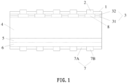
- the present invention provides a bifacial P-type PERC solar cell which consecutively includes a rear silver electrode 1, a rear aluminum grid 2, a rear passivation layer 3, P-type silicon 4, an N-type emitter 5, a front silicon nitride film 6, and a front silver electrode 7.
- a first laser grooving region 8 is formed in the rear passivation layer 3 by laser grooving.
- the rear aluminum grid line 2 is connected to the P-type silicon 4 via the first laser grooving region 8.
- the front silver electrode 7 includes a front silver electrode busbar 7A and a front silver electrode finger 7B.
- the rear passivation layer 3 includes an aluminum oxide layer 31 and a silicon nitride layer 32.
- the present invention improves the existing monofacial PERC solar cells and provides many back aluminum grid lines 2 in replacement of the all-aluminum back electric field.
- Laser grooving regions 8 are provided in the rear passivation layer 3 with a laser grooving technique, and the rear aluminum grid lines 2 are printed on these parallel-arranged laser grooving regions 8 to be in local contact with the P-type silicon 4.
- the rear aluminum grid lines 2 arranged in dense and parallel manner can play a role of increasing the open-circuit voltage Voc and the short-circuit current Jsc, reducing the recombination rate of the minority carriers, and thus enhancing the photoelectric conversion efficiency of the cell, to replace the all-aluminum back electric field in the existing monofacial cell structure.
- the rear surface of the silicon wafer is not completely covered by the rear aluminum grid lines 2, sunlight can be projected into the silicon wafer between the rear aluminum grid lines 2. Accordingly, the rear surface of the silicon wafer can absorb the light energy, which greatly improves the photoelectric conversion efficiency of the cell.
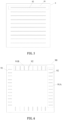
- the first laser grooving region 8 includes a plurality of groups of first laser grooving units 81 arranged horizontally; a plurality of laser grooving units 81 are arranged in a vertical direction, each group of first laser grooving unit 81 includes one or more first laser grooving bodies 82 arranged horizontally.
- the rear aluminum grid lines 2 are perpendicular to the first laser grooving body 82.
- the dashed boxes shown in FIGS. 4 and 5 are the first laser grooving unit 81, and each group of first laser grooving unit 81 includes one or more first laser grooving bodies 82 arranged horizontally.
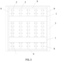
- an outer aluminum grid frame 9 is arranged at the periphery of the rear aluminum grid lines in the present invention, wherein the outer aluminum grid frame 9 is connected with the rear aluminum grid lines 2 and the rear silver electrode 1.
- the outer aluminum grid frame 9 provides an additional transmission path for electrons, thus preventing the problems of broken grid lines in the EL test due to the broken aluminum lines and low photoelectric conversion efficiency.
- a second laser grooving region 90 may be provided below the outer aluminum grid frame 9 with reference to the first embodiment of the rear surface structure shown in FIG. 3 .
- the outer aluminum grid frame 9 may also be provided without the second laser grooving region 90 disposed below (see the second embodiment of the rear surface structure shown in FIG. 2 ).
- the second laser grooving region 90 includes second laser grooving units 91 arranged vertically or horizontally, and each group of the second laser grooving unit 91 contains one or more second laser grooving bodies 92 arranged vertically or horizontally.
- the outer aluminum grid frame 9 is perpendicular to the second laser grooving body 92.
- the second laser grooving region 90 includes two second laser grooving units 91A arranged vertically and two second laser grooving units 91B arranged horizontally, wherein the second laser grooving unit 91A arranged vertically includes a plurality of second laser grooving bodies 92 arranged horizontally, and the second laser grooving unit 91B arranged horizontally includes a plurality of second laser grooving bodies 92 arranged vertically.
- the second laser grooving region 90 is provided, it is unnecessary to precisely align the aluminum paste with the second laser grooving region, which simplifies the laser and printing processes and lowers the difficulty in debugging the printing device.
- the second laser grooving region outside the region covered by the aluminum paste can increase sunlight absorption at the rear surface of the cell and boost the photoelectric conversion efficiency of the cell.
- first laser grooving units 81 have various implementations including:
- each group of the first laser grooving units 81 contains a plurality of first laser grooving bodies 82 arranged horizontally, there are a few possibilities as follows:
- the first laser grooving body has a linear shape to facilitate fabrication, simplify process and lower manufacturing costs.
- the first laser grooving body also can be configured in other shapes, such as a curved shape, an arc shape, a wavy shape, etc. Its implementations are not limited to the embodiments presented in this invention.
- the first laser grooving units 81 are arranged in parallel and the first laser grooving bodies 82 are arranged side by side in each first laser grooving unit 81, which can simplify the production process and is suitable for mass application.
- Spacing between the first laser grooving units 81 is 0.5-50mm and spacing between the first laser grooving bodies 82 is 0.5-50mm in each first laser grooving unit 81.
- the first laser grooving body 82 has a length of 50-5000 micron and a width of 10-500 micron. Preferably, the first laser grooving body 82 is 250-1200 micron long and 30-80 micron wide.
- the length, width and spacing of the first laser grooving units 81 and the number and width of the aluminum grids are optimized based on the comprehensive consideration of contact area between the aluminum grid and the P-type silicon, shading area of the aluminum grid, and sufficient collection of electrons, with the purpose of reducing the shading area of the rear aluminum grids as much as possible, while ensuring good current output and further boosting the overall photoelectric conversion efficiency of the cell.
- the number of the rear aluminum grid lines 2 is 30-500 and each rear aluminum grid line 2 has a width of 30-500 micron, wherein the width of the rear aluminum grid line 2 is much smaller than a length of the first laser grooving body 82.
- the number of the rear aluminum grid lines 2 is 80-200 and each rear aluminum grid line 2 has a width of 50-300 micron.
- the width of the rear aluminum grid line is much smaller than the length of the first laser grooving body, which may greatly facilitate the printing of the rear aluminum grid lines if the aluminum grid is perpendicular to the first laser grooving body.
- the aluminum grid can be provided within the first laser grooving region without precise alignment, which simplifies the laser and printing processes, lowers the difficulty in debugging the printing device and is easy to scale-up for industrial production.
- the rear aluminum grid lines are achieved by forming a first laser grooving region in the rear passivation layer with laser grooving and then printing the aluminum paste in a direction perpendicular to the laser scribing direction, such that the aluminum paste is connected with the P-type silicon via the grooving region.
- the bifacial PERC solar cell may employ a method different from the conventional one for printing the aluminum paste, without the need of precisely aligning the aluminum paste with the first laser grooving region. Such process is simple and easy to scale-up for industrial production.
- the yield can be boosted to 99.5%.
- the rear passivation layer 3 includes an aluminum oxide layer 31 and a silicon nitride layer 32, wherein the aluminum oxide layer 31 is connected with the P-type silicon 4 and the silicon nitride layer 32 is connected with the aluminum oxide layer 31;
- the present invention also discloses a method of preparing a bifacial P-type PERC solar cell, comprising:
- S106 may be performed before S104 and S105.
- S109 and S110 can be combined into one step, i.e., the rear aluminum grid line and the outer aluminum grid frame are completed in a single printing.
- S103 and S104 there is also included a step of polishing the rear surface of the silicon wafer.
- the present invention may be provided with or without the step of polishing the rear surface.
- a second laser grooving region may be or may not be provided below the outer aluminum grid frame. If the second laser grooving region is present, the step (7) also includes: performing laser grooving in the rear surface of the silicon wafer to form a second laser grooving region, wherein the second laser grooving region includes second laser grooving units arranged vertically or horizontally, and each group of the second laser grooving units contains one or more second laser grooving bodies arranged vertically or horizontally; the second laser grooving bodies are perpendicular to the outer aluminum grid frame.
- the present invention also discloses a PERC solar cell module, which includes a PERC solar cell and a packaging material, wherein the PERC solar cell is any one of the bifacial P-type PERC solar cells described above.
- the PERC solar cell module it is composed of a first high-transmittance tempered glass, a first layer of ethylene-vinyl acetate (EVA) copolymer, a PERC solar cell, a second layer of an ethylene-vinyl acetate (EVA) copolymer, and a second high-transmittance tempered glass which are sequentially connected from top to bottom.
- EVA ethylene-vinyl acetate
- the present invention also discloses a PERC solar system, which includes a PERC solar cell that is any one of the bifacial P-type PERC solar cells described above.
- a PERC solar system includes a PERC solar cell, a rechargeable battery pack, a charge and discharge controller, an inverter, an AC power distribution cabinet, and a sun-tracking control system.
- the PERC solar system therein may be provided with or without a rechargeable battery pack, a charge and discharge controller, and an inverter.
- Those skilled in the art can adopt different settings according to actual needs.
Landscapes
- Photovoltaic Devices (AREA)
- Life Sciences & Earth Sciences (AREA)
- Engineering & Computer Science (AREA)
- Sustainable Energy (AREA)
- Sustainable Development (AREA)
Applications Claiming Priority (2)
| Application Number | Priority Date | Filing Date | Title |
|---|---|---|---|
| CN201710122418.3A CN107425080B (zh) | 2017-03-03 | 2017-03-03 | P型perc双面太阳能电池及其组件、系统和制备方法 |
| PCT/CN2018/077585 WO2018157821A1 (zh) | 2017-03-03 | 2018-02-28 | P型perc双面太阳能电池及其组件、系统和制备方法 |
Publications (3)
| Publication Number | Publication Date |
|---|---|
| EP3588585A1 EP3588585A1 (en) | 2020-01-01 |
| EP3588585A4 EP3588585A4 (en) | 2021-01-06 |
| EP3588585B1 true EP3588585B1 (en) | 2023-02-22 |
Family
ID=60423137
Family Applications (1)
| Application Number | Title | Priority Date | Filing Date |
|---|---|---|---|
| EP18760676.9A Active EP3588585B1 (en) | 2017-03-03 | 2018-02-28 | P-type perc double-sided solar cell, assembly thereof, system thereof and preparation method therefor |
Country Status (6)
| Country | Link |
|---|---|
| US (1) | US20200127149A1 (https=) |
| EP (1) | EP3588585B1 (https=) |
| JP (1) | JP7023975B2 (https=) |
| KR (1) | KR102323459B1 (https=) |
| CN (1) | CN107425080B (https=) |
| WO (1) | WO2018157821A1 (https=) |
Families Citing this family (9)
| Publication number | Priority date | Publication date | Assignee | Title |
|---|---|---|---|---|
| CN107425080B (zh) * | 2017-03-03 | 2019-11-15 | 广东爱康太阳能科技有限公司 | P型perc双面太阳能电池及其组件、系统和制备方法 |
| CN107039543B (zh) * | 2017-03-03 | 2019-10-22 | 广东爱康太阳能科技有限公司 | P型perc双面太阳能电池及其组件、系统和制备方法 |
| CN109638110A (zh) * | 2018-12-18 | 2019-04-16 | 韩华新能源(启东)有限公司 | 一种基于双面PERC电池片背面SiNx多层膜结构的制备方法 |
| CN109616556A (zh) * | 2018-12-18 | 2019-04-12 | 韩华新能源(启东)有限公司 | 一种硅片背面退火和正面镀膜一体化的方法以及一种电池片的制备方法 |
| CN109888053B (zh) * | 2019-01-03 | 2021-08-31 | 天津爱旭太阳能科技有限公司 | P型perc双面太阳能电池对位印刷方法、制备方法及电池 |
| CN112510099B (zh) * | 2020-11-30 | 2022-05-20 | 晶科能源(海宁)有限公司 | 太阳能电池组件、太阳能电池片及其制造方法 |
| CN115084299B (zh) * | 2022-06-23 | 2024-10-01 | 广东爱旭科技有限公司 | 一种p型太阳能电池及其制作方法、电池组件和光伏系统 |
| CN117352572A (zh) * | 2022-06-28 | 2024-01-05 | 四川省普照光新能源有限公司 | 一种氧化锌-晶硅叠层太阳能电池及其制备方法 |
| CN121078846A (zh) * | 2025-06-06 | 2025-12-05 | 浙江晶科能源有限公司 | 光伏电池及其制造方法、叠层电池、光伏组件 |
Family Cites Families (27)
| Publication number | Priority date | Publication date | Assignee | Title |
|---|---|---|---|---|
| DE102009053776A1 (de) * | 2009-11-19 | 2011-06-01 | Systaic Cells Gmbh | Emitterbildung mit einem Laser |
| JP5495777B2 (ja) * | 2009-12-25 | 2014-05-21 | 京セラ株式会社 | 太陽電池モジュール |
| KR20140126819A (ko) * | 2013-04-22 | 2014-11-03 | 엘지전자 주식회사 | 태양 전지 |
| CN103489934B (zh) * | 2013-09-25 | 2016-03-02 | 晶澳(扬州)太阳能科技有限公司 | 一种双面透光的局部铝背场太阳能电池及其制备方法 |
| CN203883015U (zh) * | 2014-04-11 | 2014-10-15 | 东莞职业技术学院 | 一种晶硅太阳能电池栅线 |
| DE102014105358A1 (de) * | 2014-04-15 | 2015-10-15 | Solarworld Innovations Gmbh | Solarzelle und Verfahren zum Herstellen einer Solarzelle |
| CN203983300U (zh) * | 2014-06-04 | 2014-12-03 | 浙江尖山光电股份有限公司 | 一种环形细栅多晶电池片 |
| KR20150144585A (ko) * | 2014-06-17 | 2015-12-28 | 엘지전자 주식회사 | 태양 전지의 후처리 장치 |
| CN203932078U (zh) * | 2014-07-17 | 2014-11-05 | 中利腾晖光伏科技有限公司 | 一种背钝化太阳能电池 |
| TWI518932B (zh) * | 2014-07-24 | 2016-01-21 | 茂迪股份有限公司 | 太陽能電池及其模組 |
| CN104201214A (zh) | 2014-08-21 | 2014-12-10 | 广东爱康太阳能科技有限公司 | 一种背面钝化太阳能电池及其制备方法 |
| WO2016068237A1 (ja) * | 2014-10-29 | 2016-05-06 | 京セラ株式会社 | 太陽電池モジュール |
| US9722104B2 (en) | 2014-11-28 | 2017-08-01 | Lg Electronics Inc. | Solar cell and method for manufacturing the same |
| DE102014118332A1 (de) | 2014-12-10 | 2016-06-16 | Solarworld Innovations Gmbh | Photovoltaikmodul |
| DE202015101360U1 (de) * | 2015-03-17 | 2015-03-26 | Solarworld Innovations Gmbh | Solarzelle |
| DE102015104236B4 (de) * | 2015-03-20 | 2021-11-18 | Fraunhofer-Gesellschaft zur Förderung der angewandten Forschung e.V. | Photovoltaische Solarzelle |
| DE202015004065U1 (de) * | 2015-06-09 | 2015-07-30 | Solarworld Innovations Gmbh | Solarzellenanordnung |
| CN205335274U (zh) * | 2015-12-31 | 2016-06-22 | 广东爱康太阳能科技有限公司 | 一种局部铝背场的晶体硅太阳能电池 |
| CN105702758A (zh) * | 2016-04-14 | 2016-06-22 | 泰州中来光电科技有限公司 | 背结n型太阳能电池的制备方法及其电池和组件、系统 |
| CN105810769B (zh) * | 2016-05-24 | 2019-02-22 | 晋能清洁能源科技股份公司 | 一种背钝化太阳能电池的激光开槽结构 |
| CN106098839B (zh) * | 2016-06-15 | 2018-03-23 | 浙江正泰太阳能科技有限公司 | 一种高效晶硅perc电池的制备方法 |
| CN106449834B (zh) * | 2016-10-08 | 2018-01-23 | 苏州阿特斯阳光电力科技有限公司 | 一种双面perc太阳能电池片背面栅线结构 |
| CN106252445B (zh) * | 2016-10-08 | 2019-04-23 | 苏州阿特斯阳光电力科技有限公司 | 一种双面perc太阳能电池片背面的栅线结构 |
| CN106449877A (zh) * | 2016-10-17 | 2017-02-22 | 浙江晶科能源有限公司 | 一种perc电池的制备方法 |
| CN106887475B (zh) * | 2017-03-03 | 2019-07-05 | 广东爱旭科技股份有限公司 | P型perc双面太阳能电池及其组件、系统和制备方法 |
| CN106876497B (zh) * | 2017-03-03 | 2019-12-31 | 广东爱康太阳能科技有限公司 | P型perc双面太阳能电池的制备方法 |
| CN107425080B (zh) * | 2017-03-03 | 2019-11-15 | 广东爱康太阳能科技有限公司 | P型perc双面太阳能电池及其组件、系统和制备方法 |
-
2017
- 2017-03-03 CN CN201710122418.3A patent/CN107425080B/zh active Active
-
2018
- 2018-02-28 US US16/490,874 patent/US20200127149A1/en not_active Abandoned
- 2018-02-28 WO PCT/CN2018/077585 patent/WO2018157821A1/zh not_active Ceased
- 2018-02-28 EP EP18760676.9A patent/EP3588585B1/en active Active
- 2018-02-28 JP JP2019547982A patent/JP7023975B2/ja active Active
- 2018-02-28 KR KR1020197029113A patent/KR102323459B1/ko not_active Expired - Fee Related
Also Published As
| Publication number | Publication date |
|---|---|
| JP7023975B2 (ja) | 2022-02-22 |
| WO2018157821A1 (zh) | 2018-09-07 |
| EP3588585A1 (en) | 2020-01-01 |
| CN107425080B (zh) | 2019-11-15 |
| CN107425080A (zh) | 2017-12-01 |
| KR102323459B1 (ko) | 2021-11-08 |
| KR20200005535A (ko) | 2020-01-15 |
| US20200127149A1 (en) | 2020-04-23 |
| JP2020509601A (ja) | 2020-03-26 |
| EP3588585A4 (en) | 2021-01-06 |
Similar Documents
| Publication | Publication Date | Title |
|---|---|---|
| EP3588585B1 (en) | P-type perc double-sided solar cell, assembly thereof, system thereof and preparation method therefor | |
| EP3591714B1 (en) | P-type perc double-sided solar cell, assembly thereof, system thereof and preparation method therefor | |
| EP3591715B1 (en) | Method of preparing a bifacial p-type perc solar cell | |
| EP3588583A1 (en) | P-type perc double-sided solar cell and module and system thereof, and preparation method therefor | |
| CN106887476B (zh) | P型perc双面太阳能电池及其组件、系统和制备方法 | |
| CN106876497B (zh) | P型perc双面太阳能电池的制备方法 | |
| CN107039543B (zh) | P型perc双面太阳能电池及其组件、系统和制备方法 | |
| CN206931606U (zh) | P型perc双面太阳能电池及其组件、系统 | |
| CN206628482U (zh) | P型perc双面太阳能电池及其组件、系统 | |
| CN206921828U (zh) | P型perc双面太阳能电池及其组件、系统 | |
| KR20120081417A (ko) | 태양전지 및 그 제조방법 | |
| CN206921829U (zh) | P型perc双面太阳能电池及其组件、系统 |
Legal Events
| Date | Code | Title | Description |
|---|---|---|---|
| STAA | Information on the status of an ep patent application or granted ep patent |
Free format text: STATUS: THE INTERNATIONAL PUBLICATION HAS BEEN MADE |
|
| PUAI | Public reference made under article 153(3) epc to a published international application that has entered the european phase |
Free format text: ORIGINAL CODE: 0009012 |
|
| STAA | Information on the status of an ep patent application or granted ep patent |
Free format text: STATUS: REQUEST FOR EXAMINATION WAS MADE |
|
| 17P | Request for examination filed |
Effective date: 20190927 |
|
| AK | Designated contracting states |
Kind code of ref document: A1 Designated state(s): AL AT BE BG CH CY CZ DE DK EE ES FI FR GB GR HR HU IE IS IT LI LT LU LV MC MK MT NL NO PL PT RO RS SE SI SK SM TR |
|
| AX | Request for extension of the european patent |
Extension state: BA ME |
|
| DAV | Request for validation of the european patent (deleted) | ||
| DAX | Request for extension of the european patent (deleted) | ||
| A4 | Supplementary search report drawn up and despatched |
Effective date: 20201209 |
|
| RIC1 | Information provided on ipc code assigned before grant |
Ipc: H01L 31/18 20060101ALI20201203BHEP Ipc: H01L 31/0224 20060101AFI20201203BHEP Ipc: H01L 31/068 20120101ALI20201203BHEP |
|
| GRAP | Despatch of communication of intention to grant a patent |
Free format text: ORIGINAL CODE: EPIDOSNIGR1 |
|
| STAA | Information on the status of an ep patent application or granted ep patent |
Free format text: STATUS: GRANT OF PATENT IS INTENDED |
|
| INTG | Intention to grant announced |
Effective date: 20220901 |
|
| GRAS | Grant fee paid |
Free format text: ORIGINAL CODE: EPIDOSNIGR3 |
|
| GRAA | (expected) grant |
Free format text: ORIGINAL CODE: 0009210 |
|
| STAA | Information on the status of an ep patent application or granted ep patent |
Free format text: STATUS: THE PATENT HAS BEEN GRANTED |
|
| AK | Designated contracting states |
Kind code of ref document: B1 Designated state(s): AL AT BE BG CH CY CZ DE DK EE ES FI FR GB GR HR HU IE IS IT LI LT LU LV MC MK MT NL NO PL PT RO RS SE SI SK SM TR |
|
| REG | Reference to a national code |
Ref country code: GB Ref legal event code: FG4D |
|
| REG | Reference to a national code |
Ref country code: CH Ref legal event code: EP |
|
| REG | Reference to a national code |
Ref country code: DE Ref legal event code: R096 Ref document number: 602018046425 Country of ref document: DE |
|
| REG | Reference to a national code |
Ref country code: AT Ref legal event code: REF Ref document number: 1550075 Country of ref document: AT Kind code of ref document: T Effective date: 20230315 Ref country code: IE Ref legal event code: FG4D |
|
| REG | Reference to a national code |
Ref country code: LT Ref legal event code: MG9D |
|
| REG | Reference to a national code |
Ref country code: NL Ref legal event code: MP Effective date: 20230222 |
|
| REG | Reference to a national code |
Ref country code: DE Ref legal event code: R082 Ref document number: 602018046425 Country of ref document: DE Ref country code: DE Ref legal event code: R082 Ref document number: 602018046425 Country of ref document: DE Representative=s name: DEHNS GERMANY PARTNERSCHAFT MBB, DE |
|
| REG | Reference to a national code |
Ref country code: AT Ref legal event code: MK05 Ref document number: 1550075 Country of ref document: AT Kind code of ref document: T Effective date: 20230222 |
|
| PG25 | Lapsed in a contracting state [announced via postgrant information from national office to epo] |
Ref country code: RS Free format text: LAPSE BECAUSE OF FAILURE TO SUBMIT A TRANSLATION OF THE DESCRIPTION OR TO PAY THE FEE WITHIN THE PRESCRIBED TIME-LIMIT Effective date: 20230222 Ref country code: PT Free format text: LAPSE BECAUSE OF FAILURE TO SUBMIT A TRANSLATION OF THE DESCRIPTION OR TO PAY THE FEE WITHIN THE PRESCRIBED TIME-LIMIT Effective date: 20230622 Ref country code: NO Free format text: LAPSE BECAUSE OF FAILURE TO SUBMIT A TRANSLATION OF THE DESCRIPTION OR TO PAY THE FEE WITHIN THE PRESCRIBED TIME-LIMIT Effective date: 20230522 Ref country code: NL Free format text: LAPSE BECAUSE OF FAILURE TO SUBMIT A TRANSLATION OF THE DESCRIPTION OR TO PAY THE FEE WITHIN THE PRESCRIBED TIME-LIMIT Effective date: 20230222 Ref country code: LV Free format text: LAPSE BECAUSE OF FAILURE TO SUBMIT A TRANSLATION OF THE DESCRIPTION OR TO PAY THE FEE WITHIN THE PRESCRIBED TIME-LIMIT Effective date: 20230222 Ref country code: LT Free format text: LAPSE BECAUSE OF FAILURE TO SUBMIT A TRANSLATION OF THE DESCRIPTION OR TO PAY THE FEE WITHIN THE PRESCRIBED TIME-LIMIT Effective date: 20230222 Ref country code: HR Free format text: LAPSE BECAUSE OF FAILURE TO SUBMIT A TRANSLATION OF THE DESCRIPTION OR TO PAY THE FEE WITHIN THE PRESCRIBED TIME-LIMIT Effective date: 20230222 Ref country code: ES Free format text: LAPSE BECAUSE OF FAILURE TO SUBMIT A TRANSLATION OF THE DESCRIPTION OR TO PAY THE FEE WITHIN THE PRESCRIBED TIME-LIMIT Effective date: 20230222 Ref country code: AT Free format text: LAPSE BECAUSE OF FAILURE TO SUBMIT A TRANSLATION OF THE DESCRIPTION OR TO PAY THE FEE WITHIN THE PRESCRIBED TIME-LIMIT Effective date: 20230222 |
|
| PG25 | Lapsed in a contracting state [announced via postgrant information from national office to epo] |
Ref country code: SE Free format text: LAPSE BECAUSE OF FAILURE TO SUBMIT A TRANSLATION OF THE DESCRIPTION OR TO PAY THE FEE WITHIN THE PRESCRIBED TIME-LIMIT Effective date: 20230222 Ref country code: PL Free format text: LAPSE BECAUSE OF FAILURE TO SUBMIT A TRANSLATION OF THE DESCRIPTION OR TO PAY THE FEE WITHIN THE PRESCRIBED TIME-LIMIT Effective date: 20230222 Ref country code: IS Free format text: LAPSE BECAUSE OF FAILURE TO SUBMIT A TRANSLATION OF THE DESCRIPTION OR TO PAY THE FEE WITHIN THE PRESCRIBED TIME-LIMIT Effective date: 20230622 Ref country code: GR Free format text: LAPSE BECAUSE OF FAILURE TO SUBMIT A TRANSLATION OF THE DESCRIPTION OR TO PAY THE FEE WITHIN THE PRESCRIBED TIME-LIMIT Effective date: 20230523 Ref country code: FI Free format text: LAPSE BECAUSE OF FAILURE TO SUBMIT A TRANSLATION OF THE DESCRIPTION OR TO PAY THE FEE WITHIN THE PRESCRIBED TIME-LIMIT Effective date: 20230222 |
|
| REG | Reference to a national code |
Ref country code: BE Ref legal event code: MM Effective date: 20230228 |
|
| PG25 | Lapsed in a contracting state [announced via postgrant information from national office to epo] |
Ref country code: SM Free format text: LAPSE BECAUSE OF FAILURE TO SUBMIT A TRANSLATION OF THE DESCRIPTION OR TO PAY THE FEE WITHIN THE PRESCRIBED TIME-LIMIT Effective date: 20230222 Ref country code: RO Free format text: LAPSE BECAUSE OF FAILURE TO SUBMIT A TRANSLATION OF THE DESCRIPTION OR TO PAY THE FEE WITHIN THE PRESCRIBED TIME-LIMIT Effective date: 20230222 Ref country code: LU Free format text: LAPSE BECAUSE OF NON-PAYMENT OF DUE FEES Effective date: 20230228 Ref country code: EE Free format text: LAPSE BECAUSE OF FAILURE TO SUBMIT A TRANSLATION OF THE DESCRIPTION OR TO PAY THE FEE WITHIN THE PRESCRIBED TIME-LIMIT Effective date: 20230222 Ref country code: DK Free format text: LAPSE BECAUSE OF FAILURE TO SUBMIT A TRANSLATION OF THE DESCRIPTION OR TO PAY THE FEE WITHIN THE PRESCRIBED TIME-LIMIT Effective date: 20230222 Ref country code: CZ Free format text: LAPSE BECAUSE OF FAILURE TO SUBMIT A TRANSLATION OF THE DESCRIPTION OR TO PAY THE FEE WITHIN THE PRESCRIBED TIME-LIMIT Effective date: 20230222 |
|
| REG | Reference to a national code |
Ref country code: DE Ref legal event code: R097 Ref document number: 602018046425 Country of ref document: DE |
|
| PG25 | Lapsed in a contracting state [announced via postgrant information from national office to epo] |
Ref country code: SK Free format text: LAPSE BECAUSE OF FAILURE TO SUBMIT A TRANSLATION OF THE DESCRIPTION OR TO PAY THE FEE WITHIN THE PRESCRIBED TIME-LIMIT Effective date: 20230222 |
|
| REG | Reference to a national code |
Ref country code: IE Ref legal event code: MM4A |
|
| PLBE | No opposition filed within time limit |
Free format text: ORIGINAL CODE: 0009261 |
|
| STAA | Information on the status of an ep patent application or granted ep patent |
Free format text: STATUS: NO OPPOSITION FILED WITHIN TIME LIMIT |
|
| PG25 | Lapsed in a contracting state [announced via postgrant information from national office to epo] |
Ref country code: MC Free format text: LAPSE BECAUSE OF FAILURE TO SUBMIT A TRANSLATION OF THE DESCRIPTION OR TO PAY THE FEE WITHIN THE PRESCRIBED TIME-LIMIT Effective date: 20230222 |
|
| 26N | No opposition filed |
Effective date: 20231123 |
|
| PG25 | Lapsed in a contracting state [announced via postgrant information from national office to epo] |
Ref country code: SI Free format text: LAPSE BECAUSE OF FAILURE TO SUBMIT A TRANSLATION OF THE DESCRIPTION OR TO PAY THE FEE WITHIN THE PRESCRIBED TIME-LIMIT Effective date: 20230222 Ref country code: MC Free format text: LAPSE BECAUSE OF FAILURE TO SUBMIT A TRANSLATION OF THE DESCRIPTION OR TO PAY THE FEE WITHIN THE PRESCRIBED TIME-LIMIT Effective date: 20230222 Ref country code: IE Free format text: LAPSE BECAUSE OF NON-PAYMENT OF DUE FEES Effective date: 20230228 |
|
| PG25 | Lapsed in a contracting state [announced via postgrant information from national office to epo] |
Ref country code: BE Free format text: LAPSE BECAUSE OF NON-PAYMENT OF DUE FEES Effective date: 20230228 |
|
| PG25 | Lapsed in a contracting state [announced via postgrant information from national office to epo] |
Ref country code: IT Free format text: LAPSE BECAUSE OF FAILURE TO SUBMIT A TRANSLATION OF THE DESCRIPTION OR TO PAY THE FEE WITHIN THE PRESCRIBED TIME-LIMIT Effective date: 20230222 |
|
| REG | Reference to a national code |
Ref country code: DE Ref legal event code: R082 Ref document number: 602018046425 Country of ref document: DE Representative=s name: DEHNS GERMANY PARTNERSCHAFT MBB, DE |
|
| PG25 | Lapsed in a contracting state [announced via postgrant information from national office to epo] |
Ref country code: BG Free format text: LAPSE BECAUSE OF FAILURE TO SUBMIT A TRANSLATION OF THE DESCRIPTION OR TO PAY THE FEE WITHIN THE PRESCRIBED TIME-LIMIT Effective date: 20230222 |
|
| REG | Reference to a national code |
Ref country code: DE Ref legal event code: R079 Ref document number: 602018046425 Country of ref document: DE Free format text: PREVIOUS MAIN CLASS: H01L0031022400 Ipc: H10F0077200000 |
|
| PG25 | Lapsed in a contracting state [announced via postgrant information from national office to epo] |
Ref country code: BG Free format text: LAPSE BECAUSE OF FAILURE TO SUBMIT A TRANSLATION OF THE DESCRIPTION OR TO PAY THE FEE WITHIN THE PRESCRIBED TIME-LIMIT Effective date: 20230222 |
|
| PGFP | Annual fee paid to national office [announced via postgrant information from national office to epo] |
Ref country code: DE Payment date: 20250218 Year of fee payment: 8 |
|
| PGFP | Annual fee paid to national office [announced via postgrant information from national office to epo] |
Ref country code: CH Payment date: 20250301 Year of fee payment: 8 |
|
| PGFP | Annual fee paid to national office [announced via postgrant information from national office to epo] |
Ref country code: FR Payment date: 20250219 Year of fee payment: 8 |
|
| PGFP | Annual fee paid to national office [announced via postgrant information from national office to epo] |
Ref country code: GB Payment date: 20250218 Year of fee payment: 8 |
|
| PG25 | Lapsed in a contracting state [announced via postgrant information from national office to epo] |
Ref country code: CY Free format text: LAPSE BECAUSE OF FAILURE TO SUBMIT A TRANSLATION OF THE DESCRIPTION OR TO PAY THE FEE WITHIN THE PRESCRIBED TIME-LIMIT; INVALID AB INITIO Effective date: 20180228 |
|
| PG25 | Lapsed in a contracting state [announced via postgrant information from national office to epo] |
Ref country code: HU Free format text: LAPSE BECAUSE OF FAILURE TO SUBMIT A TRANSLATION OF THE DESCRIPTION OR TO PAY THE FEE WITHIN THE PRESCRIBED TIME-LIMIT; INVALID AB INITIO Effective date: 20180228 |
|
| PG25 | Lapsed in a contracting state [announced via postgrant information from national office to epo] |
Ref country code: TR Free format text: LAPSE BECAUSE OF FAILURE TO SUBMIT A TRANSLATION OF THE DESCRIPTION OR TO PAY THE FEE WITHIN THE PRESCRIBED TIME-LIMIT Effective date: 20230222 |