EP3587621A1 - Verfahren zur herstellung einer aluminiumleiterplatte - Google Patents
Verfahren zur herstellung einer aluminiumleiterplatte Download PDFInfo
- Publication number
- EP3587621A1 EP3587621A1 EP18758454.5A EP18758454A EP3587621A1 EP 3587621 A1 EP3587621 A1 EP 3587621A1 EP 18758454 A EP18758454 A EP 18758454A EP 3587621 A1 EP3587621 A1 EP 3587621A1
- Authority
- EP
- European Patent Office
- Prior art keywords
- base material
- equal
- metal powder
- ceramic base
- aluminum
- Prior art date
- Legal status (The legal status is an assumption and is not a legal conclusion. Google has not performed a legal analysis and makes no representation as to the accuracy of the status listed.)
- Granted
Links
- XAGFODPZIPBFFR-UHFFFAOYSA-N aluminium Chemical compound [Al] XAGFODPZIPBFFR-UHFFFAOYSA-N 0.000 title claims abstract description 92
- 229910052782 aluminium Inorganic materials 0.000 title claims abstract description 88
- 238000000034 method Methods 0.000 title claims abstract description 53
- 238000004519 manufacturing process Methods 0.000 title claims abstract description 27
- 229910052751 metal Inorganic materials 0.000 claims abstract description 160
- 239000002184 metal Substances 0.000 claims abstract description 160
- 239000000463 material Substances 0.000 claims abstract description 109
- 239000002245 particle Substances 0.000 claims abstract description 100
- 239000000843 powder Substances 0.000 claims abstract description 98
- 239000000919 ceramic Substances 0.000 claims abstract description 90
- 229910000838 Al alloy Inorganic materials 0.000 claims abstract description 24
- 238000002844 melting Methods 0.000 claims abstract description 22
- 230000008018 melting Effects 0.000 claims abstract description 22
- 238000005507 spraying Methods 0.000 claims abstract description 9
- 238000010287 warm spraying Methods 0.000 claims description 26
- 230000015572 biosynthetic process Effects 0.000 claims description 17
- 238000009826 distribution Methods 0.000 claims description 8
- SNAAJJQQZSMGQD-UHFFFAOYSA-N aluminum magnesium Chemical compound [Mg].[Al] SNAAJJQQZSMGQD-UHFFFAOYSA-N 0.000 claims description 4
- 239000012535 impurity Substances 0.000 claims description 4
- 230000001186 cumulative effect Effects 0.000 claims description 2
- IJGRMHOSHXDMSA-UHFFFAOYSA-N Atomic nitrogen Chemical compound N#N IJGRMHOSHXDMSA-UHFFFAOYSA-N 0.000 description 27
- PMHQVHHXPFUNSP-UHFFFAOYSA-M copper(1+);methylsulfanylmethane;bromide Chemical compound Br[Cu].CSC PMHQVHHXPFUNSP-UHFFFAOYSA-M 0.000 description 23
- 229910052581 Si3N4 Inorganic materials 0.000 description 17
- HQVNEWCFYHHQES-UHFFFAOYSA-N silicon nitride Chemical compound N12[Si]34N5[Si]62N3[Si]51N64 HQVNEWCFYHHQES-UHFFFAOYSA-N 0.000 description 17
- 238000012360 testing method Methods 0.000 description 16
- 229910052757 nitrogen Inorganic materials 0.000 description 13
- 229910018134 Al-Mg Inorganic materials 0.000 description 12
- 229910018467 Al—Mg Inorganic materials 0.000 description 12
- 239000002923 metal particle Substances 0.000 description 11
- 239000011261 inert gas Substances 0.000 description 10
- 239000007789 gas Substances 0.000 description 8
- 238000005219 brazing Methods 0.000 description 6
- 238000010288 cold spraying Methods 0.000 description 6
- 239000000498 cooling water Substances 0.000 description 6
- 239000011888 foil Substances 0.000 description 6
- 238000002347 injection Methods 0.000 description 6
- 239000007924 injection Substances 0.000 description 6
- FYYHWMGAXLPEAU-UHFFFAOYSA-N Magnesium Chemical compound [Mg] FYYHWMGAXLPEAU-UHFFFAOYSA-N 0.000 description 5
- 229910052749 magnesium Inorganic materials 0.000 description 5
- 239000011777 magnesium Substances 0.000 description 5
- RYGMFSIKBFXOCR-UHFFFAOYSA-N Copper Chemical compound [Cu] RYGMFSIKBFXOCR-UHFFFAOYSA-N 0.000 description 4
- -1 and the like Substances 0.000 description 4
- 239000000567 combustion gas Substances 0.000 description 4
- 238000002485 combustion reaction Methods 0.000 description 4
- 229910052802 copper Inorganic materials 0.000 description 4
- 239000010949 copper Substances 0.000 description 4
- 238000005530 etching Methods 0.000 description 4
- 239000004065 semiconductor Substances 0.000 description 4
- 229910000861 Mg alloy Inorganic materials 0.000 description 3
- QVGXLLKOCUKJST-UHFFFAOYSA-N atomic oxygen Chemical compound [O] QVGXLLKOCUKJST-UHFFFAOYSA-N 0.000 description 3
- 230000003247 decreasing effect Effects 0.000 description 3
- 229920006351 engineering plastic Polymers 0.000 description 3
- 239000000446 fuel Substances 0.000 description 3
- 238000002156 mixing Methods 0.000 description 3
- 239000001301 oxygen Substances 0.000 description 3
- 229910052760 oxygen Inorganic materials 0.000 description 3
- 239000000088 plastic resin Substances 0.000 description 3
- 238000007751 thermal spraying Methods 0.000 description 3
- XLYOFNOQVPJJNP-UHFFFAOYSA-N water Substances O XLYOFNOQVPJJNP-UHFFFAOYSA-N 0.000 description 3
- XEEYBQQBJWHFJM-UHFFFAOYSA-N Iron Chemical compound [Fe] XEEYBQQBJWHFJM-UHFFFAOYSA-N 0.000 description 2
- 239000004952 Polyamide Substances 0.000 description 2
- ATUOYWHBWRKTHZ-UHFFFAOYSA-N Propane Chemical compound CCC ATUOYWHBWRKTHZ-UHFFFAOYSA-N 0.000 description 2
- 239000000805 composite resin Substances 0.000 description 2
- 230000007423 decrease Effects 0.000 description 2
- 239000002737 fuel gas Substances 0.000 description 2
- 238000005304 joining Methods 0.000 description 2
- 238000007561 laser diffraction method Methods 0.000 description 2
- 239000007788 liquid Substances 0.000 description 2
- 238000005259 measurement Methods 0.000 description 2
- 239000002905 metal composite material Substances 0.000 description 2
- TWNQGVIAIRXVLR-UHFFFAOYSA-N oxo(oxoalumanyloxy)alumane Chemical compound O=[Al]O[Al]=O TWNQGVIAIRXVLR-UHFFFAOYSA-N 0.000 description 2
- 238000013001 point bending Methods 0.000 description 2
- 229920002647 polyamide Polymers 0.000 description 2
- 229920001707 polybutylene terephthalate Polymers 0.000 description 2
- 229920006324 polyoxymethylene Polymers 0.000 description 2
- 238000000790 scattering method Methods 0.000 description 2
- 239000007787 solid Substances 0.000 description 2
- 239000000758 substrate Substances 0.000 description 2
- PIGFYZPCRLYGLF-UHFFFAOYSA-N Aluminum nitride Chemical compound [Al]#N PIGFYZPCRLYGLF-UHFFFAOYSA-N 0.000 description 1
- OKTJSMMVPCPJKN-UHFFFAOYSA-N Carbon Chemical compound [C] OKTJSMMVPCPJKN-UHFFFAOYSA-N 0.000 description 1
- MYMOFIZGZYHOMD-UHFFFAOYSA-N Dioxygen Chemical compound O=O MYMOFIZGZYHOMD-UHFFFAOYSA-N 0.000 description 1
- 229930182556 Polyacetal Natural products 0.000 description 1
- BQCADISMDOOEFD-UHFFFAOYSA-N Silver Chemical compound [Ag] BQCADISMDOOEFD-UHFFFAOYSA-N 0.000 description 1
- 230000005856 abnormality Effects 0.000 description 1
- PNEYBMLMFCGWSK-UHFFFAOYSA-N aluminium oxide Inorganic materials [O-2].[O-2].[O-2].[Al+3].[Al+3] PNEYBMLMFCGWSK-UHFFFAOYSA-N 0.000 description 1
- 239000012159 carrier gas Substances 0.000 description 1
- 229910010293 ceramic material Inorganic materials 0.000 description 1
- 238000012512 characterization method Methods 0.000 description 1
- 238000000576 coating method Methods 0.000 description 1
- 230000000052 comparative effect Effects 0.000 description 1
- 238000001816 cooling Methods 0.000 description 1
- 230000008021 deposition Effects 0.000 description 1
- 229910001873 dinitrogen Inorganic materials 0.000 description 1
- 229910001882 dioxygen Inorganic materials 0.000 description 1
- 238000007598 dipping method Methods 0.000 description 1
- 230000000694 effects Effects 0.000 description 1
- 238000005516 engineering process Methods 0.000 description 1
- 230000003628 erosive effect Effects 0.000 description 1
- 239000010419 fine particle Substances 0.000 description 1
- 229910002804 graphite Inorganic materials 0.000 description 1
- 239000010439 graphite Substances 0.000 description 1
- 238000000227 grinding Methods 0.000 description 1
- 238000010438 heat treatment Methods 0.000 description 1
- 239000001307 helium Substances 0.000 description 1
- 229910052734 helium Inorganic materials 0.000 description 1
- SWQJXJOGLNCZEY-UHFFFAOYSA-N helium atom Chemical compound [He] SWQJXJOGLNCZEY-UHFFFAOYSA-N 0.000 description 1
- 229910052742 iron Inorganic materials 0.000 description 1
- 239000003350 kerosene Substances 0.000 description 1
- 239000003915 liquefied petroleum gas Substances 0.000 description 1
- 238000012423 maintenance Methods 0.000 description 1
- 150000002739 metals Chemical class 0.000 description 1
- 150000004767 nitrides Chemical class 0.000 description 1
- 230000003647 oxidation Effects 0.000 description 1
- 238000007254 oxidation reaction Methods 0.000 description 1
- 239000004033 plastic Substances 0.000 description 1
- 229920003023 plastic Polymers 0.000 description 1
- 229920000515 polycarbonate Polymers 0.000 description 1
- 239000004417 polycarbonate Substances 0.000 description 1
- 229920001955 polyphenylene ether Polymers 0.000 description 1
- 238000012545 processing Methods 0.000 description 1
- 239000001294 propane Substances 0.000 description 1
- 230000009257 reactivity Effects 0.000 description 1
- 239000011347 resin Substances 0.000 description 1
- 229920005989 resin Polymers 0.000 description 1
- 229910052709 silver Inorganic materials 0.000 description 1
- 239000004332 silver Substances 0.000 description 1
- 238000004088 simulation Methods 0.000 description 1
- 239000000243 solution Substances 0.000 description 1
- 239000007921 spray Substances 0.000 description 1
- 239000000126 substance Substances 0.000 description 1
Images


Classifications
-
- C—CHEMISTRY; METALLURGY
- C23—COATING METALLIC MATERIAL; COATING MATERIAL WITH METALLIC MATERIAL; CHEMICAL SURFACE TREATMENT; DIFFUSION TREATMENT OF METALLIC MATERIAL; COATING BY VACUUM EVAPORATION, BY SPUTTERING, BY ION IMPLANTATION OR BY CHEMICAL VAPOUR DEPOSITION, IN GENERAL; INHIBITING CORROSION OF METALLIC MATERIAL OR INCRUSTATION IN GENERAL
- C23C—COATING METALLIC MATERIAL; COATING MATERIAL WITH METALLIC MATERIAL; SURFACE TREATMENT OF METALLIC MATERIAL BY DIFFUSION INTO THE SURFACE, BY CHEMICAL CONVERSION OR SUBSTITUTION; COATING BY VACUUM EVAPORATION, BY SPUTTERING, BY ION IMPLANTATION OR BY CHEMICAL VAPOUR DEPOSITION, IN GENERAL
- C23C24/00—Coating starting from inorganic powder
- C23C24/02—Coating starting from inorganic powder by application of pressure only
- C23C24/04—Impact or kinetic deposition of particles
-
- H—ELECTRICITY
- H05—ELECTRIC TECHNIQUES NOT OTHERWISE PROVIDED FOR
- H05K—PRINTED CIRCUITS; CASINGS OR CONSTRUCTIONAL DETAILS OF ELECTRIC APPARATUS; MANUFACTURE OF ASSEMBLAGES OF ELECTRICAL COMPONENTS
- H05K3/00—Apparatus or processes for manufacturing printed circuits
- H05K3/10—Apparatus or processes for manufacturing printed circuits in which conductive material is applied to the insulating support in such a manner as to form the desired conductive pattern
- H05K3/14—Apparatus or processes for manufacturing printed circuits in which conductive material is applied to the insulating support in such a manner as to form the desired conductive pattern using spraying techniques to apply the conductive material, e.g. vapour evaporation
-
- B—PERFORMING OPERATIONS; TRANSPORTING
- B32—LAYERED PRODUCTS
- B32B—LAYERED PRODUCTS, i.e. PRODUCTS BUILT-UP OF STRATA OF FLAT OR NON-FLAT, e.g. CELLULAR OR HONEYCOMB, FORM
- B32B15/00—Layered products comprising a layer of metal
- B32B15/04—Layered products comprising a layer of metal comprising metal as the main or only constituent of a layer, which is next to another layer of the same or of a different material
-
- B—PERFORMING OPERATIONS; TRANSPORTING
- B32—LAYERED PRODUCTS
- B32B—LAYERED PRODUCTS, i.e. PRODUCTS BUILT-UP OF STRATA OF FLAT OR NON-FLAT, e.g. CELLULAR OR HONEYCOMB, FORM
- B32B15/00—Layered products comprising a layer of metal
- B32B15/20—Layered products comprising a layer of metal comprising aluminium or copper
-
- C—CHEMISTRY; METALLURGY
- C22—METALLURGY; FERROUS OR NON-FERROUS ALLOYS; TREATMENT OF ALLOYS OR NON-FERROUS METALS
- C22C—ALLOYS
- C22C21/00—Alloys based on aluminium
- C22C21/06—Alloys based on aluminium with magnesium as the next major constituent
-
- C—CHEMISTRY; METALLURGY
- C23—COATING METALLIC MATERIAL; COATING MATERIAL WITH METALLIC MATERIAL; CHEMICAL SURFACE TREATMENT; DIFFUSION TREATMENT OF METALLIC MATERIAL; COATING BY VACUUM EVAPORATION, BY SPUTTERING, BY ION IMPLANTATION OR BY CHEMICAL VAPOUR DEPOSITION, IN GENERAL; INHIBITING CORROSION OF METALLIC MATERIAL OR INCRUSTATION IN GENERAL
- C23C—COATING METALLIC MATERIAL; COATING MATERIAL WITH METALLIC MATERIAL; SURFACE TREATMENT OF METALLIC MATERIAL BY DIFFUSION INTO THE SURFACE, BY CHEMICAL CONVERSION OR SUBSTITUTION; COATING BY VACUUM EVAPORATION, BY SPUTTERING, BY ION IMPLANTATION OR BY CHEMICAL VAPOUR DEPOSITION, IN GENERAL
- C23C24/00—Coating starting from inorganic powder
- C23C24/08—Coating starting from inorganic powder by application of heat or pressure and heat
- C23C24/082—Coating starting from inorganic powder by application of heat or pressure and heat without intermediate formation of a liquid in the layer
- C23C24/085—Coating with metallic material, i.e. metals or metal alloys, optionally comprising hard particles, e.g. oxides, carbides or nitrides
- C23C24/087—Coating with metal alloys or metal elements only
-
- H—ELECTRICITY
- H05—ELECTRIC TECHNIQUES NOT OTHERWISE PROVIDED FOR
- H05K—PRINTED CIRCUITS; CASINGS OR CONSTRUCTIONAL DETAILS OF ELECTRIC APPARATUS; MANUFACTURE OF ASSEMBLAGES OF ELECTRICAL COMPONENTS
- H05K1/00—Printed circuits
- H05K1/02—Details
- H05K1/03—Use of materials for the substrate
- H05K1/0306—Inorganic insulating substrates, e.g. ceramic, glass
-
- H—ELECTRICITY
- H05—ELECTRIC TECHNIQUES NOT OTHERWISE PROVIDED FOR
- H05K—PRINTED CIRCUITS; CASINGS OR CONSTRUCTIONAL DETAILS OF ELECTRIC APPARATUS; MANUFACTURE OF ASSEMBLAGES OF ELECTRICAL COMPONENTS
- H05K3/00—Apparatus or processes for manufacturing printed circuits
- H05K3/10—Apparatus or processes for manufacturing printed circuits in which conductive material is applied to the insulating support in such a manner as to form the desired conductive pattern
- H05K3/102—Apparatus or processes for manufacturing printed circuits in which conductive material is applied to the insulating support in such a manner as to form the desired conductive pattern by bonding of conductive powder, i.e. metallic powder
-
- H—ELECTRICITY
- H05—ELECTRIC TECHNIQUES NOT OTHERWISE PROVIDED FOR
- H05K—PRINTED CIRCUITS; CASINGS OR CONSTRUCTIONAL DETAILS OF ELECTRIC APPARATUS; MANUFACTURE OF ASSEMBLAGES OF ELECTRICAL COMPONENTS
- H05K2203/00—Indexing scheme relating to apparatus or processes for manufacturing printed circuits covered by H05K3/00
- H05K2203/13—Moulding and encapsulation; Deposition techniques; Protective layers
- H05K2203/1333—Deposition techniques, e.g. coating
- H05K2203/1344—Spraying small metal particles or droplets of molten metal
Definitions
- the present invention relates to a method for manufacturing an aluminum circuit board. Further, the present invention relates to an aluminum circuit board and an electronic device using the method for manufacturing the aluminum circuit board.
- An aluminum circuit board including a ceramic base material such as alumina, and a circuit layer formed on both surfaces of the ceramic base material has been practically realized as a semiconductor device that is used in a power module or the like.
- the ceramic base material for a ceramic circuit board has been required to higher heat conductivity, in addition to high electrical insulating properties.
- the application of the ceramic base material having high heat conductivity such as aluminum nitride, has been considered.
- a copper circuit is provided on the ceramic base material having high heat conductivity, there is a problem that a crack tends to be easily generated in the vicinity of a joining portion between the ceramic base material and the copper circuit, due to repeated heat cycles or a temperature change in the service environment during the operation of such semiconductor element.
- Patent Literature 3 3
- Non Patent Literature 1 Integrated characterization of cold sprayed aluminum coatings, W.B. Choi, L. Li, V. Luzin, R. Neiser, T. Gnaupel-Herold, H.J. Prask, S. Sampath, A. Gouldstone, Acta Materialia, Volume 55, Issue 3, February 2007, Page 857-866
- the brazing method it is necessary to join the ceramic board material with the aluminum foil or the aluminum alloy foil at a high temperature by applying a pressure over all the area all the time.
- the pressurization is performed by mechanical means such as by placing the laminated body in a graphite jig, and pushing from both end surfaces by screwing. In such a method, there is a problem that productivity is not sufficiently high.
- An aluminum layer can also be formed by conventional thermal spraying methods in which powder is melted and is sprayed to a base material.
- a problem_that aluminum has high reactivity with oxygen and nitrogen at a high temperature above the melting point, and thus, in a conventional thermal spraying device where thermal spraying is performed in the atmosphere, a film having a low density and rich in oxide and nitride is formed.
- warm spraying has been also considered as one of new methods of forming metal layers.
- the warm spraying method is a technology in which film formation is performed by spraying metal powder to a base material at a high velocity, along with carrier gas that is heated within the temperature range to soften the metal powder (for example, refer to Patent Literature 4).
- the present invention has been made in consideration of the circumstances described above, and a main object thereof is to provide a method in which it is possible to easily manufacture an aluminum circuit board including a metal layer that contains aluminum and/or an aluminum alloy, and is formed on a ceramic base material with high adhesiveness.
- One aspect of the present invention provides a method for manufacturing an aluminum circuit board, including: a step of spraying heated metal powder containing aluminum particles and/or aluminum alloy particles to a ceramic base material, and thereby forming a metal layer on a surface of the ceramic base material.
- the temperature of at least a part of the metal powder is higher than or equal to the softening temperature of the metal powder and lower than or equal to the melting point of the metal powder at a time point of reaching the surface of the ceramic base material.
- the softening temperature is a temperature that is defined as a value of melting point ⁇ 0.6 in the absolute temperature scale.
- the velocity of at least a part of the metal powder is greater than or equal to 450 m/s and less than or equal to 1000 m/s at the time point of reaching the surface of the ceramic base material.
- a metal layer that contains aluminum and/or an aluminum alloy and has high adhesiveness can be easily formed on the surface of a ceramic base material.
- the velocity of the metal powder is less than 450 m/s, there is a tendency that the formed metal layer on the surface of the ceramic base material tends to easily peel off, or its adhesion to the base plate tends to be insufficient.
- the velocity of the metal powder is greater than 1000 m/s, there is a tendency that the metal layer that is already attached onto the surface of the ceramic base material tends to be removed by erosion.
- the velocity of the metal powder at the time point of reaching the surface of the ceramic base material may be greater than or equal to 750 m/s and less than or equal to 900 m/s.
- the temperature of the metal powder is lower than the softening temperature, the deformation of the metal powder is suppressed, and there is a tendency that the adhesiveness of the metal powder to the ceramic base material and the density of the metal layer decrease.
- the temperature of the metal powder is higher than the melting point, there is a tendency that the metal powder is oxidized, and in particular, when the velocity of the metal powder is high, there is a tendency that the metal powder that collides with the ceramic base material is disintegrated and blown away, and thus, it is difficult to form a metal layer.
- a particle diameter D 10 which is the diameter at which 10% of the sample's mass is comprised of particles with a diameter less than this value may be greater than or equal to 10 ⁇ m
- the particle diameter D 90 of a cumulative mass percentage of 90% D 90 which is the diameter at which 90% of the sample's mass is comprised of particles with a diameter less than this value, may be less than or equal to 50 ⁇ m.
- D 10 of the metal powder may be greater than or equal to 20 ⁇ m, and D 90 of the metal powder may be less than or equal to 45 ⁇ m.
- the aluminum particles and the aluminum alloy particles are respectively metal particles containing aluminum and an aluminum alloy as their main component.
- the main component indicates a component that is contained at a ratio of greater than or equal to 90 mass% with respect to the whole.
- a ratio of the main component may be greater than or equal to 95 mass%.
- the aluminum alloy particles may be particles formed of aluminum as the main component, with magnesium, and residual inevitable impurities.
- the content of magnesium may be less than or equal to 7.5 mass% on the basis of the mass of the aluminum alloy particles.
- the metal powder be heated such that the temperature of most (for example, greater than or equal to 80 mass% of the total amount) of the metal powder sprayed onto the ceramic base material is higher than or equal to the softening temperature of the metal powder and lower than or equal to the melting point of the metal powder at the time point of reaching the surface of the ceramic base material.
- the ratio of metal powder of which the temperature at the time point of reaching the surface of the ceramic base material is lower than the softening temperature of the metal powder may be less than or equal to 10 mass%
- the ratio of metal powder of which the temperature at the time point of reaching the surface of the ceramic base material is higher than the melting point of the metal powder may be less than or equal to 10 mass%
- the temperature of the rest of the metal powder at the time point of reaching the surface of the ceramic base material may be higher than or equal to the softening temperature of the metal powder and lower than or equal to the melting point of the metal powder.
- the metal powder may contain aluminum alloy particles.
- the method for manufacturing the aluminum circuit board may further include: a step of spraying a first metal layer formed on the surface of the ceramic base material, and thereby forming a second metal layer on the surface of the first metal layer.
- the thickness of the first metal layer may be less than or equal to 150 ⁇ m. Since aluminum alloy (in particular, an aluminum-magnesium alloy) has high adhesiveness with respect to the ceramic base material as compared to aluminum, it is preferred that the first metal layer directly provided on the surface of the ceramic base material contain aluminum alloy as the main component.
- an aluminum circuit board including: a ceramic base material; and a metal layer formed by performing film formation of metal powder containing aluminum particles and/or aluminum alloy particles on a surface of the ceramic base material by the warm spraying method.
- the electric resistivity of the metal layer is less than or equal to 5 ⁇ 10 -8 ⁇ m.
- the electric resistivity of the metal layer may be less than or equal to 4 ⁇ 10 -8 ⁇ m.
- a lower limit of the electric resistivity of the metal layer is not particularly specified, but in general, is greater than 2.65 ⁇ 10 -8 ⁇ m.
- Still another aspect of the present invention provides an electronic device, including the aluminum circuit board described above.
- the method for manufacturing an aluminum circuit board of the present invention has advantages that aluminum and ceramic are joined together without using molten aluminum or a brazing material, and by using a mask, it is possible to manufacture an aluminum circuit board without etching.
- the present invention is capable of manufacturing a metal layer having higher adhesiveness and smaller electric resistance with superior efficiency for mass production.
- a “powder” used in the present specification indicates an aggregate having fluidity that is configured of a plurality of particles having different particle diameters.
- a laser diffraction and scattering method is widely used, and the methods of measurement and description of the results thereof are based on JIS Z 8825 "Particle Diameter Analysis-Laser Diffraction and Scattering Method".
- particle diameter D 10 indicates the diameter at which 10% of the sample's mass is comprised of particles with a diameter less than this value.
- particle diameter D 90 indicates the diameter at which 90% of the sample's mass is comprised of particles with a diameter less than this value.
- D 50 as defined as above is referred to as the median diameter.
- FIG. 1 is a sectional view illustrating an embodiment of an aluminum circuit board.
- An aluminum circuit board 50 illustrated in FIG. 1 includes a ceramic base material 1, and metal layers 3a and 3b that are respectively provided with being in contact with both surfaces of the ceramic base material 1.
- Each of the metal layers 3a and 3b is a layer that is formed by spraying heated metal powder, and usually has a circuit pattern that is connected to a semiconductor element. The details of a method for forming the metal layers 3a and 3b will be described below.
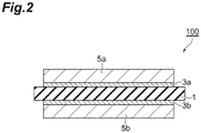
- FIG. 2 is also a sectional view illustrating another embodiment of an aluminum circuit board.
- the aluminum circuit board 100 illustrated in FIG. 2 further includes second metal layers 5a and 5b in addition to the same configuration as that of the aluminum circuit board 50, that are provided on the surfaces of the metal layers 3a and 3b attached to the ceramic base material and used as the first metal layers respectively.
- the second metal layers 5a and 5b can configure a circuit layer.
- the thickness of the metal layers 3a and 3b is not particularly limited, and for example, may be from 200 ⁇ m to 600 ⁇ m. Similarly, the total thickness of the metal layers 3a and 3b as the first metal layer, and the second metal layers 5a and 5b, for example, may be from 200 ⁇ m to 600 ⁇ m. The thickness of the metal layers 3a and 3b as the first metal layer may be less than or equal to 150 ⁇ m.
- the ceramic base material 1 can be selected from ceramic materials having suitable insulating properties.
- the ceramic base material 1 should also has high thermal conductivity, and examples thereof include aluminum nitride (AlN), silicon nitride (Si 3 N 4 ), and aluminum oxide (Al 2 O 3 ).
- the thickness of the ceramic base material 1 is not particularly limited, and for example, may be from 0.2 mm to 1.0 mm.
- FIG. 3 is a schematic view illustrating an embodiment of a method for manufacturing the aluminum circuit board exemplified in FIG. 1 or FIG. 2 .
- metal powder P consisting of many metal particles is heated, and is accelerated to a predetermined velocity by a warm spraying device 10, and is sprayed to the surface of the ceramic base material 1.
- the metal particles P may be aluminum particles, aluminum alloy particles, or a combination thereof.
- the aluminum alloy particles may be particles formed of aluminum, magnesium of less than or equal to 7.5 mass% on the basis of the mass of the aluminum alloy particles, and residual inevitable impurities.
- the warm spraying device 10 includes a tubular body 20, a fuel inlet 21, an oxygen inlet 22, an ignition plug 23, a cooling water inlet 24, a cooling water outlet 25, an inert gas inlet 26, and a powder feed port 27.
- the tubular body 20 includes a combustion chamber 11, a mixing chamber 12, an outlet nozzle 13, and a barrel portion 14.
- An injection port 15 is provided at the end of the barrel portion 14.
- fuel gas FG such as gasified liquid fuel that may be kerosene or the like or propane gas or liquefied petroleum gas is mixed with oxygen gas O 2 , and the mixed gas is ignited by the ignition plug 23. As the mixed gas is combusted, the temperature and pressure of the combustion gas increases.
- inert gas IG is fed and mixed into the combustion gas flowing out from the combustion chamber 11 in order to adjust the combustion gas temperature.
- outlet nozzle 13 thus generated high-temperature and high-pressure mixed gas expands through a divergent nozzle, and becomes a high-velocity jet, and thus, is ejected to the barrel portion 14.
- the barrel portion 14 is a straight cylindrical barrel connected to the outlet nozzle 13 in a continuous manner.
- the metal particles P i.e., the metal powder, are fed from the powder feed port 27 provided between the outlet nozzle 13 and the barrel portion 14 to the inlet of the barrel portion 14.
- the whole body of the warm spraying device is cooled by cooling water.
- the metal particles P are sprayed towards the ceramic base material 1 from the injection port 15 at a high speed, along with the mixed gas of the combustion gas and the inert gas IG, and thus, the metal particles P are deposited on the ceramic base material 1, and the metal layer 3 a is formed.
- the temperature of at least a part of the metal powder sprayed to the ceramic base material 1 be higher than or equal to a softening temperature of the metal powder and lower than or equal to the melting point of the metal powder when reaching the surface of the ceramic base material 1.
- the softening temperature is defined as a value of melting point ⁇ 0.6 in the absolute temperature scale.
- the velocity of at least a part of the metal powder sprayed to the ceramic base material 1 be greater than or equal to 450 m/s and less than or equal to 1000 m/s when reaching the surface of the ceramic base material 1.
- the ratio of metal powder of which the temperature at the time point of reaching the surface of the ceramic base material 1 is lower than or equal to the softening temperature of the metal powder may be less than or equal to 10 mass%
- the ratio of metal powder of which the temperature at the time point of reaching the surface of the ceramic base material 1 is higher than the melting point of the metal powder may be less than or equal to 10 mass%
- the temperature of the rest of the metal powder at the time point of reaching the surface of the ceramic base material may be higher than or equal to the softening temperature of the metal powder and lower than or equal to the melting point of the metal powder.
- the temperature and the velocity of the metal particles P (or the metal powder) at the time point of reaching the surface of the ceramic base material 1 can be adjusted by suitably changing the particle size distribution of the metal powder, the flow rate of the inert gas, the distance between the injection port 15 and the surface of the ceramic base material 1, and the like.
- the distance between the injection port 15 and the surface of the ceramic base material 1 is set to be in a range of 100 mm to 400 mm.
- a method for forming the second metal layer is not limited to the method described above, and may be identical to or different from that of the first metal layer.
- a second metal powder containing aluminum particles as its main component may be fed to the warm spraying method of which the condition is suitably set, to form the second metal layer.
- FIG. 4 is microscopic photographs of aluminum particles that are attached onto a surface of an aluminum nitride base material. These samples were prepared by scanning a warm spraying device over the aluminum nitride base material at a high velocity while minimizing the feed rate of the aluminum particles, and thereby spraying a small amount of aluminum particles to the surface of the aluminum nitride base material. While changing the nitrogen flow rate of the warm spraying device in three steps of 1000 SLM, 1500 SLM, and 2000 SLM, the preheating temperature of the aluminum nitride base material for each nitrogen flow rate was changed in three steps of 300K (without preheating, RT), 473K, and 673K. As shown in FIG.
- SLM is an abbreviation of standard liter/min, and is a unit indicating a gas flow rate (liter) per 1 minute at 1 atm and 0°C.
- FIG. 5 is a graph in which the ultrasonic irradiation time is plotted on the horizontal axis, whereas the ratio of dropped-out particles on a silicon nitride substrate at three levels of nitrogen flow rates and three levels of preheating temperatures are plotted on the vertical axis.
- more than 80% of the particles were dropped out by irradiation of 1 minute at a nitrogen flow rate of 2000 SLM. It was observed that the dropout rate decreased as the nitrogen flow rate decreased, that is, the adhesion of the particles was improved.
- the preheating temperature of the ceramic base material to which the metal powder is sprayed may be from 200°C to 600°C.
- FIG. 6 is a graph showing the relationship between the velocity and the temperature of aluminum particles that are generated by the warm spraying device 10 for fabrication of metal layers.
- the graph of FIG. 6 shows such relationship of velocity and temperature for particles with three different diameters, i.e., 10 ⁇ m, 30 ⁇ m, and 50 ⁇ m, which appear as three curves.
- the relationship between the velocity and the temperature of the aluminum particles at the time point of reaching the surface of the ceramic base material is plotted for different flow rates of the inert gas IG (nitrogen gas) such as 500 SLM, 1000 SLM, 1500 SLM, and 2000 SLM in the warm spraying device 10 in FIG. 6 .
- the distance between the injection port 15 of the warm spraying device 10 and the base material surface is set to 200 mm, and the velocity and the temperature of the aluminum particles at the time point of reaching the surface of the ceramic base material was calculated by a numerical simulation.
- FIG. 6 also shows the melting point (660°C, 933K) and the softening temperature (287°C, 560K) of aluminum particles.
- D 10 is greater than or equal to 10 ⁇ m, and D 90 is less than or equal to 50 ⁇ m for the particle diameter distribution of the metal powder used for the warm spraying device. It is more preferable that D 10 is greater than or equal to 20 ⁇ m, and D 90 is less than or equal to 45 ⁇ m.
- the board may be a metal composite board containing a combination of ceramic and metals such as copper, aluminum, silver, and the like, or a resin composite board containing a combination of ceramic and a resin such as an engineering plastic resin.
- a metal layer is formed on the surface of the ceramic base material that is usually provided as the outermost layer.
- the engineering plastic resin to be combined with the ceramic base material may be polyacetal (POM), polyamide (PA), polycarbonate (PC), modified polyphenylene ether (m-PPE), or polybutylene terephthalate (PBT).
- the aluminum circuit board as described above is useful as a member configuring various electronic devices.
- an aluminum nitride base material (Size: 60 mm ⁇ 50 mm ⁇ 0.635 mmt, Three-Point Bending Strength: 500 MPa, Heat Conductivity: 150 W/mK, and Purity: greater than or equal to 95%) and a silicon nitride base material (Size: 60 mm ⁇ 50 mm ⁇ 0.635 mmt, Three-Point Bending Strength: 700 MPa, Heat Conductivity: 70 W/mK, and Purity: greater than or equal to 92%) were used as the ceramic base material.
- the following film formation test was performed by using a warm spraying device having the same configuration as that illustrated in FIG. 3 .
- the aluminum nitride base material was covered with an iron mask with an opening.
- Aluminum powder manufactured by Fukuda Metal Foil & Powder Co., Ltd., a water atomized powder, Purity: 99.7%, Particle Diameter: less than or equal to 45 ⁇ m, and Melting Point: 933K
- a metal layer having a predetermined pattern 56 mm ⁇ 46 mm ⁇ 300 ⁇ mt
- Nitrogen was used as inert gas for the warm spraying method.
- a metal layer was also formed on the opposite surface of the aluminum nitride base material.
- the warm spraying condition was set to realize particle temperatures and particle velocities as shown in Table 1.
- the particle temperature and the particle velocity are these values of most of the aluminum powder at a time point of reaching the base material (the same applies to Film Formation Test 2).
- Film formation of a first metal layer using an aluminum-magnesium alloy powder was performed using the warm spraying condition shown in Table 1 in the same manner with Film Formation Test 1.
- the aluminum-magnesium alloy powder manufactured by Kojundo Chemical Lab. Co., Ltd., a gas atomized powder, Magnesium Content: 3.0 mass%, Amount of Impurities Other than Aluminum and Magnesium: less than or equal to 0.1 mass%, Particle Diameter: less than or equal to 45 ⁇ m, and Melting Point: 913K was used instead of the aluminum powder.
- Aluminum powder manufactured by Fukuda Metal Foil & Powder Co., Ltd., a water atomized powder, Purity: 99.7%, and Particle Diameter: less than or equal to 45 ⁇ m
- a second metal layer 56 mm ⁇ 46 mm ⁇ 200 ⁇ mt
- nitrogen was used as inert gas, and the condition corresponded to Particle Temperature: 500°C and Particle Velocity: 800 m/s.
- Second metal layer Particle temp. (K) Particle velocity (m/s) Particle type Thickness ( ⁇ m) Film formation availability Particle Type Thickness ( ⁇ m) 1 AlN 530 900 Al 300 Unavailable - - 2 AlN 560 400 Al 300 Unavailable - - 3 AlN 560 500 Al 300 Available - - 4 AlN 930 900 Al 300 Available - - 5 AlN 930 1100 Al 300 Unavailable - - 6 AlN 960 500 Al 300 Unavailable - - 7 Si 3 N 4 530 500 Al 300 Unavailable - - 8 Si 3 N 4 560 900 Al 300 Available - - 9 Si 3 N 4 560 1100 Al 300 Unavailable - 10 Si 3 N 4 930 400 Al 300 Unavailable - - 11 Si 3 N 4 930 500 Al 300 Available - - 12 Si 3 N 4 960 900 Al 300 Unavailable - - 13 AlN 530 900 Al-Mg 150 Unavailable - 14 AlN 560 400 Al
- test bodies were subjected to a heat cycle test.
- "at 180°C for 30 minutes, and then, at -45°C for 30 minutes” was set as one cycle, and a test of 1000 cycles was performed.
- abnormality such as peeling did not occur in the metal layers.
- the present invention is useful for manufacturing an aluminum circuit board that includes a circuit containing aluminum. Processing conditions such as the amount of metal powder and its heating temperature can be suitably managed to manufacture a circuit board including a resin composite board of ceramic and an engineering plastic resin as well as a metal composite board of ceramic and a metal.
- the method of the present invention is excellent in mass productivity and general versatility.
Landscapes
- Chemical & Material Sciences (AREA)
- Engineering & Computer Science (AREA)
- Organic Chemistry (AREA)
- Materials Engineering (AREA)
- Mechanical Engineering (AREA)
- Metallurgy (AREA)
- Microelectronics & Electronic Packaging (AREA)
- Chemical Kinetics & Catalysis (AREA)
- Manufacturing & Machinery (AREA)
- Inorganic Chemistry (AREA)
- Ceramic Engineering (AREA)
- Other Surface Treatments For Metallic Materials (AREA)
- Laminated Bodies (AREA)
- Manufacturing Of Printed Wiring (AREA)
- Coating By Spraying Or Casting (AREA)
Applications Claiming Priority (2)
| Application Number | Priority Date | Filing Date | Title |
|---|---|---|---|
| JP2017033784 | 2017-02-24 | ||
| PCT/JP2018/006488 WO2018155564A1 (ja) | 2017-02-24 | 2018-02-22 | アルミニウム回路基板の製造方法 |
Publications (3)
| Publication Number | Publication Date |
|---|---|
| EP3587621A1 true EP3587621A1 (de) | 2020-01-01 |
| EP3587621A4 EP3587621A4 (de) | 2020-01-22 |
| EP3587621B1 EP3587621B1 (de) | 2021-12-15 |
Family
ID=63252694
Family Applications (1)
| Application Number | Title | Priority Date | Filing Date |
|---|---|---|---|
| EP18758454.5A Active EP3587621B1 (de) | 2017-02-24 | 2018-02-22 | Verfahren zur herstellung einer aluminiumleiterplatte |
Country Status (5)
| Country | Link |
|---|---|
| US (1) | US11570901B2 (de) |
| EP (1) | EP3587621B1 (de) |
| JP (1) | JP6999117B2 (de) |
| CN (1) | CN110382738B (de) |
| WO (1) | WO2018155564A1 (de) |
Families Citing this family (2)
| Publication number | Priority date | Publication date | Assignee | Title |
|---|---|---|---|---|
| CN113025025B (zh) * | 2021-03-17 | 2022-03-01 | 广州鹿山新材料股份有限公司 | A2级防火铝塑板芯材及其制备方法和铝塑板 |
| CN115464152B (zh) * | 2022-08-15 | 2024-01-23 | 盐城工学院 | 一种基于复合材料增材制造低缺陷金属陶瓷零部件的方法 |
Family Cites Families (19)
| Publication number | Priority date | Publication date | Assignee | Title |
|---|---|---|---|---|
| US484533A (en) * | 1892-10-18 | gottschalk | ||
| WO1991019016A1 (en) * | 1990-05-19 | 1991-12-12 | Institut Teoreticheskoi I Prikladnoi Mekhaniki Sibirskogo Otdelenia Akademii Nauk Sssr | Method and device for coating |
| JP2642574B2 (ja) | 1992-12-17 | 1997-08-20 | 同和鉱業株式会社 | セラミックス電子回路基板の製造方法 |
| JP4293406B2 (ja) | 1999-05-28 | 2009-07-08 | 電気化学工業株式会社 | 回路基板 |
| JP4087090B2 (ja) * | 2001-09-18 | 2008-05-14 | 株式会社東芝 | 機能性素子の実装基板 |
| US6808817B2 (en) * | 2002-03-15 | 2004-10-26 | Delphi Technologies, Inc. | Kinetically sprayed aluminum metal matrix composites for thermal management |
| JP4140593B2 (ja) * | 2004-09-21 | 2008-08-27 | 住友電気工業株式会社 | メタライズ基板 |
| JP2006179856A (ja) * | 2004-11-25 | 2006-07-06 | Fuji Electric Holdings Co Ltd | 絶縁基板および半導体装置 |
| CN100406614C (zh) | 2005-03-09 | 2008-07-30 | 沈阳工业大学 | 一种镁合金表面防护层的喷涂工艺 |
| JP5098109B2 (ja) | 2005-03-28 | 2012-12-12 | 独立行政法人物質・材料研究機構 | 皮膜形成方法 |
| JP5321942B2 (ja) * | 2008-02-29 | 2013-10-23 | 新東工業株式会社 | 電子回路基板の製造方法およびその電子回路基板 |
| JP5359644B2 (ja) * | 2009-07-23 | 2013-12-04 | 三菱マテリアル株式会社 | パワーモジュール用基板、パワーモジュール及びパワーモジュール用基板の製造方法 |
| JP2012153581A (ja) * | 2011-01-27 | 2012-08-16 | Taiyo Nippon Sanso Corp | セラミックスとアルミニウムとの接合方法 |
| JP5548167B2 (ja) | 2011-07-11 | 2014-07-16 | 日本発條株式会社 | 積層体及び積層体の製造方法 |
| JP5809901B2 (ja) * | 2011-09-20 | 2015-11-11 | 日本発條株式会社 | 積層体及び積層体の製造方法 |
| JP2013071873A (ja) | 2011-09-28 | 2013-04-22 | Nhk Spring Co Ltd | 接合体 |
| JP6096094B2 (ja) | 2013-10-28 | 2017-03-15 | 日本発條株式会社 | 積層体、絶縁性冷却板、パワーモジュールおよび積層体の製造方法 |
| JP6347104B2 (ja) * | 2013-12-27 | 2018-06-27 | セイコーエプソン株式会社 | 電気配線層の製造方法、電気配線層形成用部材、電気配線層、電気配線基板の製造方法、電気配線基板形成用部材、電気配線基板、振動子、電子機器および移動体 |
| JP6400501B2 (ja) * | 2015-02-18 | 2018-10-03 | Dowaメタルテック株式会社 | 金属−セラミックス回路基板の製造方法 |
-
2018
- 2018-02-22 CN CN201880013217.2A patent/CN110382738B/zh active Active
- 2018-02-22 WO PCT/JP2018/006488 patent/WO2018155564A1/ja unknown
- 2018-02-22 US US16/488,776 patent/US11570901B2/en active Active
- 2018-02-22 JP JP2019501418A patent/JP6999117B2/ja active Active
- 2018-02-22 EP EP18758454.5A patent/EP3587621B1/de active Active
Also Published As
| Publication number | Publication date |
|---|---|
| EP3587621A4 (de) | 2020-01-22 |
| CN110382738A (zh) | 2019-10-25 |
| US11570901B2 (en) | 2023-01-31 |
| US20200120809A1 (en) | 2020-04-16 |
| JPWO2018155564A1 (ja) | 2019-12-12 |
| WO2018155564A1 (ja) | 2018-08-30 |
| EP3587621B1 (de) | 2021-12-15 |
| CN110382738B (zh) | 2022-04-08 |
| JP6999117B2 (ja) | 2022-01-18 |
Similar Documents
| Publication | Publication Date | Title |
|---|---|---|
| US5648123A (en) | Process for producing a strong bond between copper layers and ceramic | |
| US4911987A (en) | Metal/ceramic or ceramic/ceramic bonded structure | |
| US20060251823A1 (en) | Kinetic spray application of coatings onto covered materials | |
| US20050085030A1 (en) | Kinetically sprayed aluminum metal matrix composites for thermal management | |
| EP2285752A1 (de) | Kontinuierliche oder diskrete metallisierungsschicht auf einem keramiksubstrat | |
| CN108206100B (zh) | 用于电气装置的触点组件以及其制作方法 | |
| EP3587621B1 (de) | Verfahren zur herstellung einer aluminiumleiterplatte | |
| CN111454080A (zh) | 一种敷铜或敷铜合金氧化铝陶瓷基板及其制备方法 | |
| JP2008300455A (ja) | パワーモジュール | |
| CN110169213B (zh) | 陶瓷电路基板的制造方法 | |
| KR101013078B1 (ko) | 저온분사법을 이용한 전극의 제조방법 및 이에 의한 전극 | |
| EP3572555B1 (de) | Verfahren zur herstellung einer keramischen leiterplatte | |
| KR20130132984A (ko) | 온도 제어 요소 및 온도 제어 요소에 전자 부품을 부착하기 위한 방법 | |
| KR20130051289A (ko) | 저온분사 코팅방법 및 이에 의해 제조되는 코팅층 | |
| JP2012153581A (ja) | セラミックスとアルミニウムとの接合方法 | |
| KR100682740B1 (ko) | 반도체 제조설비의 코팅층 형성방법 | |
| Bobzin et al. | Electrical contacting of high-velocity-air-fuel sprayed NiCr20 coatings by brazing | |
| EP1678990A2 (de) | Verfahren und vorrichtung zur herstellung elektrischer schaltungen | |
| JP6378247B2 (ja) | 積層体、パワーモジュールおよび積層体の製造方法 | |
| JP7538845B2 (ja) | 積層体、及び、パワーモジュール | |
| KR101569807B1 (ko) | 이중 분사주조 장치 | |
| JP2017071835A (ja) | 窒化アルミニウムの皮膜製造方法及びその方法により製造される窒化アルミニウム皮膜 | |
| KR20060123143A (ko) | 고체 플레이팅재 제조 방법 및 그 고체 플레이팅재 | |
| KR101535063B1 (ko) | 이중 분사주조 장치 | |
| KR20090069523A (ko) | 코팅층의 형성방법 |
Legal Events
| Date | Code | Title | Description |
|---|---|---|---|
| STAA | Information on the status of an ep patent application or granted ep patent |
Free format text: STATUS: THE INTERNATIONAL PUBLICATION HAS BEEN MADE |
|
| PUAI | Public reference made under article 153(3) epc to a published international application that has entered the european phase |
Free format text: ORIGINAL CODE: 0009012 |
|
| STAA | Information on the status of an ep patent application or granted ep patent |
Free format text: STATUS: REQUEST FOR EXAMINATION WAS MADE |
|
| 17P | Request for examination filed |
Effective date: 20190903 |
|
| AK | Designated contracting states |
Kind code of ref document: A1 Designated state(s): AL AT BE BG CH CY CZ DE DK EE ES FI FR GB GR HR HU IE IS IT LI LT LU LV MC MK MT NL NO PL PT RO RS SE SI SK SM TR |
|
| AX | Request for extension of the european patent |
Extension state: BA ME |
|
| A4 | Supplementary search report drawn up and despatched |
Effective date: 20191219 |
|
| RIC1 | Information provided on ipc code assigned before grant |
Ipc: H05K 1/00 20060101ALI20191213BHEP Ipc: H05K 1/09 20060101ALI20191213BHEP Ipc: H05K 3/00 20060101ALI20191213BHEP Ipc: C23C 24/04 20060101AFI20191213BHEP Ipc: H01K 1/02 20060101ALI20191213BHEP Ipc: C23C 24/08 20060101ALI20191213BHEP Ipc: H05K 3/14 20060101ALI20191213BHEP Ipc: B32B 15/20 20060101ALI20191213BHEP Ipc: B32B 15/04 20060101ALI20191213BHEP |
|
| DAV | Request for validation of the european patent (deleted) | ||
| DAX | Request for extension of the european patent (deleted) | ||
| STAA | Information on the status of an ep patent application or granted ep patent |
Free format text: STATUS: EXAMINATION IS IN PROGRESS |
|
| 17Q | First examination report despatched |
Effective date: 20200826 |
|
| STAA | Information on the status of an ep patent application or granted ep patent |
Free format text: STATUS: EXAMINATION IS IN PROGRESS |
|
| RIC1 | Information provided on ipc code assigned before grant |
Ipc: C23C 24/04 20060101AFI20210609BHEP Ipc: B32B 15/04 20060101ALI20210609BHEP Ipc: B32B 15/20 20060101ALI20210609BHEP Ipc: H05K 1/09 20060101ALI20210609BHEP Ipc: H05K 3/14 20060101ALI20210609BHEP Ipc: C23C 24/08 20060101ALI20210609BHEP Ipc: H01K 1/02 20060101ALI20210609BHEP Ipc: H05K 1/00 20060101ALI20210609BHEP Ipc: H05K 3/00 20060101ALI20210609BHEP |
|
| GRAP | Despatch of communication of intention to grant a patent |
Free format text: ORIGINAL CODE: EPIDOSNIGR1 |
|
| STAA | Information on the status of an ep patent application or granted ep patent |
Free format text: STATUS: GRANT OF PATENT IS INTENDED |
|
| RIC1 | Information provided on ipc code assigned before grant |
Ipc: C23C 24/04 20060101AFI20210706BHEP Ipc: B32B 15/04 20060101ALI20210706BHEP Ipc: B32B 15/20 20060101ALI20210706BHEP Ipc: H05K 1/09 20060101ALI20210706BHEP Ipc: H05K 3/14 20060101ALI20210706BHEP Ipc: C23C 24/08 20060101ALI20210706BHEP Ipc: H01K 1/02 20060101ALI20210706BHEP Ipc: H05K 1/00 20060101ALI20210706BHEP Ipc: H05K 3/00 20060101ALI20210706BHEP Ipc: H05K 1/03 20060101ALI20210706BHEP Ipc: H05K 3/10 20060101ALI20210706BHEP |
|
| INTG | Intention to grant announced |
Effective date: 20210721 |
|
| GRAS | Grant fee paid |
Free format text: ORIGINAL CODE: EPIDOSNIGR3 |
|
| GRAA | (expected) grant |
Free format text: ORIGINAL CODE: 0009210 |
|
| STAA | Information on the status of an ep patent application or granted ep patent |
Free format text: STATUS: THE PATENT HAS BEEN GRANTED |
|
| AK | Designated contracting states |
Kind code of ref document: B1 Designated state(s): AL AT BE BG CH CY CZ DE DK EE ES FI FR GB GR HR HU IE IS IT LI LT LU LV MC MK MT NL NO PL PT RO RS SE SI SK SM TR |
|
| REG | Reference to a national code |
Ref country code: GB Ref legal event code: FG4D Ref country code: CH Ref legal event code: EP |
|
| REG | Reference to a national code |
Ref country code: IE Ref legal event code: FG4D Ref country code: DE Ref legal event code: R096 Ref document number: 602018028245 Country of ref document: DE |
|
| REG | Reference to a national code |
Ref country code: AT Ref legal event code: REF Ref document number: 1455558 Country of ref document: AT Kind code of ref document: T Effective date: 20220115 |
|
| REG | Reference to a national code |
Ref country code: LT Ref legal event code: MG9D |
|
| REG | Reference to a national code |
Ref country code: NL Ref legal event code: MP Effective date: 20211215 |
|
| PG25 | Lapsed in a contracting state [announced via postgrant information from national office to epo] |
Ref country code: RS Free format text: LAPSE BECAUSE OF FAILURE TO SUBMIT A TRANSLATION OF THE DESCRIPTION OR TO PAY THE FEE WITHIN THE PRESCRIBED TIME-LIMIT Effective date: 20211215 Ref country code: LT Free format text: LAPSE BECAUSE OF FAILURE TO SUBMIT A TRANSLATION OF THE DESCRIPTION OR TO PAY THE FEE WITHIN THE PRESCRIBED TIME-LIMIT Effective date: 20211215 Ref country code: FI Free format text: LAPSE BECAUSE OF FAILURE TO SUBMIT A TRANSLATION OF THE DESCRIPTION OR TO PAY THE FEE WITHIN THE PRESCRIBED TIME-LIMIT Effective date: 20211215 Ref country code: BG Free format text: LAPSE BECAUSE OF FAILURE TO SUBMIT A TRANSLATION OF THE DESCRIPTION OR TO PAY THE FEE WITHIN THE PRESCRIBED TIME-LIMIT Effective date: 20220315 |
|
| REG | Reference to a national code |
Ref country code: AT Ref legal event code: MK05 Ref document number: 1455558 Country of ref document: AT Kind code of ref document: T Effective date: 20211215 |
|
| PG25 | Lapsed in a contracting state [announced via postgrant information from national office to epo] |
Ref country code: SE Free format text: LAPSE BECAUSE OF FAILURE TO SUBMIT A TRANSLATION OF THE DESCRIPTION OR TO PAY THE FEE WITHIN THE PRESCRIBED TIME-LIMIT Effective date: 20211215 Ref country code: NO Free format text: LAPSE BECAUSE OF FAILURE TO SUBMIT A TRANSLATION OF THE DESCRIPTION OR TO PAY THE FEE WITHIN THE PRESCRIBED TIME-LIMIT Effective date: 20220315 Ref country code: LV Free format text: LAPSE BECAUSE OF FAILURE TO SUBMIT A TRANSLATION OF THE DESCRIPTION OR TO PAY THE FEE WITHIN THE PRESCRIBED TIME-LIMIT Effective date: 20211215 Ref country code: HR Free format text: LAPSE BECAUSE OF FAILURE TO SUBMIT A TRANSLATION OF THE DESCRIPTION OR TO PAY THE FEE WITHIN THE PRESCRIBED TIME-LIMIT Effective date: 20211215 Ref country code: GR Free format text: LAPSE BECAUSE OF FAILURE TO SUBMIT A TRANSLATION OF THE DESCRIPTION OR TO PAY THE FEE WITHIN THE PRESCRIBED TIME-LIMIT Effective date: 20220316 |
|
| PG25 | Lapsed in a contracting state [announced via postgrant information from national office to epo] |
Ref country code: NL Free format text: LAPSE BECAUSE OF FAILURE TO SUBMIT A TRANSLATION OF THE DESCRIPTION OR TO PAY THE FEE WITHIN THE PRESCRIBED TIME-LIMIT Effective date: 20211215 |
|
| PG25 | Lapsed in a contracting state [announced via postgrant information from national office to epo] |
Ref country code: SM Free format text: LAPSE BECAUSE OF FAILURE TO SUBMIT A TRANSLATION OF THE DESCRIPTION OR TO PAY THE FEE WITHIN THE PRESCRIBED TIME-LIMIT Effective date: 20211215 Ref country code: SK Free format text: LAPSE BECAUSE OF FAILURE TO SUBMIT A TRANSLATION OF THE DESCRIPTION OR TO PAY THE FEE WITHIN THE PRESCRIBED TIME-LIMIT Effective date: 20211215 Ref country code: RO Free format text: LAPSE BECAUSE OF FAILURE TO SUBMIT A TRANSLATION OF THE DESCRIPTION OR TO PAY THE FEE WITHIN THE PRESCRIBED TIME-LIMIT Effective date: 20211215 Ref country code: PT Free format text: LAPSE BECAUSE OF FAILURE TO SUBMIT A TRANSLATION OF THE DESCRIPTION OR TO PAY THE FEE WITHIN THE PRESCRIBED TIME-LIMIT Effective date: 20220418 Ref country code: ES Free format text: LAPSE BECAUSE OF FAILURE TO SUBMIT A TRANSLATION OF THE DESCRIPTION OR TO PAY THE FEE WITHIN THE PRESCRIBED TIME-LIMIT Effective date: 20211215 Ref country code: EE Free format text: LAPSE BECAUSE OF FAILURE TO SUBMIT A TRANSLATION OF THE DESCRIPTION OR TO PAY THE FEE WITHIN THE PRESCRIBED TIME-LIMIT Effective date: 20211215 Ref country code: CZ Free format text: LAPSE BECAUSE OF FAILURE TO SUBMIT A TRANSLATION OF THE DESCRIPTION OR TO PAY THE FEE WITHIN THE PRESCRIBED TIME-LIMIT Effective date: 20211215 |
|
| PG25 | Lapsed in a contracting state [announced via postgrant information from national office to epo] |
Ref country code: PL Free format text: LAPSE BECAUSE OF FAILURE TO SUBMIT A TRANSLATION OF THE DESCRIPTION OR TO PAY THE FEE WITHIN THE PRESCRIBED TIME-LIMIT Effective date: 20211215 Ref country code: AT Free format text: LAPSE BECAUSE OF FAILURE TO SUBMIT A TRANSLATION OF THE DESCRIPTION OR TO PAY THE FEE WITHIN THE PRESCRIBED TIME-LIMIT Effective date: 20211215 |
|
| REG | Reference to a national code |
Ref country code: DE Ref legal event code: R097 Ref document number: 602018028245 Country of ref document: DE |
|
| PG25 | Lapsed in a contracting state [announced via postgrant information from national office to epo] |
Ref country code: MC Free format text: LAPSE BECAUSE OF FAILURE TO SUBMIT A TRANSLATION OF THE DESCRIPTION OR TO PAY THE FEE WITHIN THE PRESCRIBED TIME-LIMIT Effective date: 20211215 Ref country code: IS Free format text: LAPSE BECAUSE OF FAILURE TO SUBMIT A TRANSLATION OF THE DESCRIPTION OR TO PAY THE FEE WITHIN THE PRESCRIBED TIME-LIMIT Effective date: 20220415 |
|
| PLBE | No opposition filed within time limit |
Free format text: ORIGINAL CODE: 0009261 |
|
| STAA | Information on the status of an ep patent application or granted ep patent |
Free format text: STATUS: NO OPPOSITION FILED WITHIN TIME LIMIT |
|
| REG | Reference to a national code |
Ref country code: BE Ref legal event code: MM Effective date: 20220228 |
|
| PG25 | Lapsed in a contracting state [announced via postgrant information from national office to epo] |
Ref country code: LU Free format text: LAPSE BECAUSE OF NON-PAYMENT OF DUE FEES Effective date: 20220222 Ref country code: DK Free format text: LAPSE BECAUSE OF FAILURE TO SUBMIT A TRANSLATION OF THE DESCRIPTION OR TO PAY THE FEE WITHIN THE PRESCRIBED TIME-LIMIT Effective date: 20211215 Ref country code: AL Free format text: LAPSE BECAUSE OF FAILURE TO SUBMIT A TRANSLATION OF THE DESCRIPTION OR TO PAY THE FEE WITHIN THE PRESCRIBED TIME-LIMIT Effective date: 20211215 |
|
| 26N | No opposition filed |
Effective date: 20220916 |
|
| GBPC | Gb: european patent ceased through non-payment of renewal fee |
Effective date: 20220315 |
|
| PG25 | Lapsed in a contracting state [announced via postgrant information from national office to epo] |
Ref country code: SI Free format text: LAPSE BECAUSE OF FAILURE TO SUBMIT A TRANSLATION OF THE DESCRIPTION OR TO PAY THE FEE WITHIN THE PRESCRIBED TIME-LIMIT Effective date: 20211215 |
|
| PG25 | Lapsed in a contracting state [announced via postgrant information from national office to epo] |
Ref country code: FR Free format text: LAPSE BECAUSE OF NON-PAYMENT OF DUE FEES Effective date: 20220228 |
|
| PG25 | Lapsed in a contracting state [announced via postgrant information from national office to epo] |
Ref country code: IE Free format text: LAPSE BECAUSE OF NON-PAYMENT OF DUE FEES Effective date: 20220222 Ref country code: GB Free format text: LAPSE BECAUSE OF NON-PAYMENT OF DUE FEES Effective date: 20220315 |
|
| PG25 | Lapsed in a contracting state [announced via postgrant information from national office to epo] |
Ref country code: BE Free format text: LAPSE BECAUSE OF NON-PAYMENT OF DUE FEES Effective date: 20220228 |
|
| PG25 | Lapsed in a contracting state [announced via postgrant information from national office to epo] |
Ref country code: IT Free format text: LAPSE BECAUSE OF FAILURE TO SUBMIT A TRANSLATION OF THE DESCRIPTION OR TO PAY THE FEE WITHIN THE PRESCRIBED TIME-LIMIT Effective date: 20211215 |
|
| P01 | Opt-out of the competence of the unified patent court (upc) registered |
Effective date: 20230511 |
|
| PG25 | Lapsed in a contracting state [announced via postgrant information from national office to epo] |
Ref country code: MK Free format text: LAPSE BECAUSE OF FAILURE TO SUBMIT A TRANSLATION OF THE DESCRIPTION OR TO PAY THE FEE WITHIN THE PRESCRIBED TIME-LIMIT Effective date: 20211215 Ref country code: CY Free format text: LAPSE BECAUSE OF FAILURE TO SUBMIT A TRANSLATION OF THE DESCRIPTION OR TO PAY THE FEE WITHIN THE PRESCRIBED TIME-LIMIT Effective date: 20211215 |
|
| PGFP | Annual fee paid to national office [announced via postgrant information from national office to epo] |
Ref country code: DE Payment date: 20240226 Year of fee payment: 7 Ref country code: CH Payment date: 20240301 Year of fee payment: 7 |
|
| PG25 | Lapsed in a contracting state [announced via postgrant information from national office to epo] |
Ref country code: HU Free format text: LAPSE BECAUSE OF FAILURE TO SUBMIT A TRANSLATION OF THE DESCRIPTION OR TO PAY THE FEE WITHIN THE PRESCRIBED TIME-LIMIT; INVALID AB INITIO Effective date: 20180222 |
|
| PG25 | Lapsed in a contracting state [announced via postgrant information from national office to epo] |
Ref country code: TR Free format text: LAPSE BECAUSE OF FAILURE TO SUBMIT A TRANSLATION OF THE DESCRIPTION OR TO PAY THE FEE WITHIN THE PRESCRIBED TIME-LIMIT Effective date: 20211215 |
|
| PG25 | Lapsed in a contracting state [announced via postgrant information from national office to epo] |
Ref country code: MT Free format text: LAPSE BECAUSE OF FAILURE TO SUBMIT A TRANSLATION OF THE DESCRIPTION OR TO PAY THE FEE WITHIN THE PRESCRIBED TIME-LIMIT Effective date: 20211215 |