EP3586214B1 - Clock divider device and methods thereof - Google Patents
Clock divider device and methods thereof Download PDFInfo
- Publication number
- EP3586214B1 EP3586214B1 EP18756852.2A EP18756852A EP3586214B1 EP 3586214 B1 EP3586214 B1 EP 3586214B1 EP 18756852 A EP18756852 A EP 18756852A EP 3586214 B1 EP3586214 B1 EP 3586214B1
- Authority
- EP
- European Patent Office
- Prior art keywords
- clock
- frequency
- stretch
- signal
- enable signals
- Prior art date
- Legal status (The legal status is an assumption and is not a legal conclusion. Google has not performed a legal analysis and makes no representation as to the accuracy of the status listed.)
- Active
Links
Images


Classifications
-
- G—PHYSICS
- G06—COMPUTING OR CALCULATING; COUNTING
- G06F—ELECTRIC DIGITAL DATA PROCESSING
- G06F1/00—Details not covered by groups G06F3/00 - G06F13/00 and G06F21/00
- G06F1/04—Generating or distributing clock signals or signals derived directly therefrom
- G06F1/10—Distribution of clock signals, e.g. skew
-
- G—PHYSICS
- G06—COMPUTING OR CALCULATING; COUNTING
- G06F—ELECTRIC DIGITAL DATA PROCESSING
- G06F1/00—Details not covered by groups G06F3/00 - G06F13/00 and G06F21/00
- G06F1/04—Generating or distributing clock signals or signals derived directly therefrom
- G06F1/08—Clock generators with changeable or programmable clock frequency
-
- G—PHYSICS
- G06—COMPUTING OR CALCULATING; COUNTING
- G06F—ELECTRIC DIGITAL DATA PROCESSING
- G06F1/00—Details not covered by groups G06F3/00 - G06F13/00 and G06F21/00
- G06F1/26—Power supply means, e.g. regulation thereof
- G06F1/30—Means for acting in the event of power-supply failure or interruption, e.g. power-supply fluctuations
- G06F1/305—Means for acting in the event of power-supply failure or interruption, e.g. power-supply fluctuations in the event of power-supply fluctuations
-
- G—PHYSICS
- G06—COMPUTING OR CALCULATING; COUNTING
- G06F—ELECTRIC DIGITAL DATA PROCESSING
- G06F1/00—Details not covered by groups G06F3/00 - G06F13/00 and G06F21/00
- G06F1/26—Power supply means, e.g. regulation thereof
- G06F1/32—Means for saving power
- G06F1/3203—Power management, i.e. event-based initiation of a power-saving mode
- G06F1/3206—Monitoring of events, devices or parameters that trigger a change in power modality
-
- G—PHYSICS
- G06—COMPUTING OR CALCULATING; COUNTING
- G06F—ELECTRIC DIGITAL DATA PROCESSING
- G06F1/00—Details not covered by groups G06F3/00 - G06F13/00 and G06F21/00
- G06F1/26—Power supply means, e.g. regulation thereof
- G06F1/32—Means for saving power
- G06F1/3203—Power management, i.e. event-based initiation of a power-saving mode
- G06F1/3234—Power saving characterised by the action undertaken
- G06F1/324—Power saving characterised by the action undertaken by lowering clock frequency
-
- G—PHYSICS
- G06—COMPUTING OR CALCULATING; COUNTING
- G06F—ELECTRIC DIGITAL DATA PROCESSING
- G06F1/00—Details not covered by groups G06F3/00 - G06F13/00 and G06F21/00
- G06F1/26—Power supply means, e.g. regulation thereof
- G06F1/32—Means for saving power
- G06F1/3203—Power management, i.e. event-based initiation of a power-saving mode
-
- Y—GENERAL TAGGING OF NEW TECHNOLOGICAL DEVELOPMENTS; GENERAL TAGGING OF CROSS-SECTIONAL TECHNOLOGIES SPANNING OVER SEVERAL SECTIONS OF THE IPC; TECHNICAL SUBJECTS COVERED BY FORMER USPC CROSS-REFERENCE ART COLLECTIONS [XRACs] AND DIGESTS
- Y02—TECHNOLOGIES OR APPLICATIONS FOR MITIGATION OR ADAPTATION AGAINST CLIMATE CHANGE
- Y02D—CLIMATE CHANGE MITIGATION TECHNOLOGIES IN INFORMATION AND COMMUNICATION TECHNOLOGIES [ICT], I.E. INFORMATION AND COMMUNICATION TECHNOLOGIES AIMING AT THE REDUCTION OF THEIR OWN ENERGY USE
- Y02D10/00—Energy efficient computing, e.g. low power processors, power management or thermal management
Definitions
- a data processing device such as an integrated circuit (IC) microprocessor device
- IC microprocessor device can include a large number of data subsystems fabricated at a single semiconductor die.
- an IC microprocessor device can include a memory interface subsystem and a graphics acceleration subsystem in addition to a central processing unit.
- Each data subsystem can operate as a data processor and can include disparate operating frequency limitations. Therefore, the computational performance of the microprocessor device is typically improved if each data subsystem is configured to operate at a respective frequency that can be different from that of another data subsystem.
- the operating frequency of a particular data subsystem can be changed efficiently while the data subsystem continues to operate.
- the microprocessor can transition a data subsystem between an active or nominal power operating mode and a low-power operating mode by altering the frequency of a clock signal provided to that data subsystem.
- FIGs. 1-4 disclose techniques for implementing clock dividers for supporting clock ramp ups and downs associated with, for example, changes in a power mode at a processor.
- Clock dividers can be built using cascaded flip flops with a multiplexer to control divided clocks for clock ramp up/down.
- the addition of flops in the clock path may increase jitter, which will have an impact on the maximum clock frequency (Fmax) that can be applied to at least one module of the processor.
- a clock divider circuit includes a transmission gate multiplexer (mux) in which the clock signal (Clkln) acts as a select signal that picks between two enable (CKGEN_EnableA and CKGEN_EnableB) inputs.
- the clock divisor can be adjusted in, for example, 0.5 divider increments (e.g., 1.0, 1.5, 2.0, 2.5, etc.) by modulating the CKGEN_EnableA and CKGEN_EnableB bits applied to the enable inputs.
- a threshold granularity e.g., 0.5 divider increments
- the clock divider supports slower clock ramp up/down during CC6 entry/exit and scan shift reset entry/exit.
- the slow ramp up/down of clock frequency enabled by the clock divider in turn provides mitigation of problems associated with rapid changes of supply current sometimes referred to herein as di/dt.
- the clock divider also enables clock stretching with reduced latency by modifying an existing enable stream of core clock enable signals upon receiving a stretch assertion signal (i.e., StretchEn) that is triggered by detecting a power supply droop.
- StretchEn a stretch assertion signal
- the CKGEN_EnableA and CKGEN_EnableB bits may be overridden by StrEn assertion (triggered by the power supply droop) to force a stretch in clock frequencies.
- the clock divider includes a duty cycle adjuster within the mux to enable duty cycle adjusting. Providing the duty cycle adjuster within the clock divider avoids adding additional stages to support duty cycle adjusting, thereby reducing jitter.
- FIG. 1 illustrates a block diagram of a processing system 100 utilizing clock dividers in accordance with at least some embodiments.
- the processing system 100 includes a compute complex 102 (also known as a "core complex"), a cache hierarchy 104, a memory controller 106, and a southbridge 108.
- the compute complex 102 includes a plurality of processor cores, such as the four processor cores 111, 112, 113, 114 depicted in the example of FIG. 1 .
- the processor cores may include central processing unit (CPU) cores, graphics processing unit (GPU) cores, digital signal processor (DSP) cores, or a combination thereof. It will be appreciated that the number of processor cores of the compute complex 102 may be fewer or more than four.
- the memory controller 106 operates as the interface between the cache hierarchy 104 and a system memory 110.
- data to be cached in the cache hierarchy 104 typically is manipulated as blocks of data referred to as "cache lines", and which are addressed or otherwise located in a memory hierarchy using a physical address of system memory 110.
- Cache lines are accessed from the system memory 110 by the memory controller 106 in response to memory requests from the cache hierarchy 104.
- the memory controller 106 manages this write-back process.
- the southbridge 108 operates as the interface between the cache hierarchy 104, the memory controller 106, and one or more peripherals (not shown) of the processing system 100 (e.g., network interfaces, keyboards, mice, displays, and other input/output devices).
- the cache hierarchy 104 includes two or more levels of caches.
- the cache hierarchy 104 includes three cache levels: level 1 (L1), level 2 (L2), and level 3 (L3).
- L1 level 1
- L2 level 2
- L3 level 3
- the core complex 102 implements small private caches for each processing core, which are depicted as L1 caches 121, 122, 123, 124, each associated with a corresponding one of processor cores 111-114 as depicted in FIG. 1 .
- the core complex 102 implements larger private caches for each processor core, which are depicted as L2 caches 131, 132, 133, 134 corresponding to processor cores 111-114, respectively, as also illustrated in FIG. 1 .
- Each of the L2 caches 131-134 is private to its corresponding processor core, but the cache hierarchy 104 operates to maintain coherency between the L2 caches 131-134.
- the L2 caches 131-134 can be direct mapped or an n-way set associative cache in some embodiments.
- the cache hierarchy 104 implements an L3 cache 140 that is shared by the processor cores of the core complex 102, and thus shared by at least the L2 caches 131-134.
- Components of the L3 cache 140 include, but is not limited to, at least one level shifter 142.
- the L3 cache 140 includes one level shifter 142 per processing core, such as when the processor cores 111-114 have different frequencies and/or voltages.
- each the four processor cores 111, 112, 113, 114 includes a clock mesh 154 (also known as a "mesh clock” or a “clock tree"), a digital frequency synthesis logic (DFS) 164, a CKGEN logic 174, and a discrete Fourier transform (DFT) logic 184.
- the processor core 114 is generally configured to execute sets of instructions (e.g., computer programs) to carry out operations on behalf of an electronic device.
- the processor core includes one or more modules, such as fetch states, dispatch stages, execution units, memory controllers, input/output interfaces, caches, and the like that are each composed of synchronous logic elements, logic gates, and other components.
- the processor core 114 employs one or more clock signals to synchronize operation of these components.
- the processor core 114 receives a synchronized version of a clock signal from the L3 cache, and the clock mesh 154 distributes various versions of the clock signal to the various components of the processor core 114.
- the level shifter 142 of the L3 cache 140 provides a P-state clock to the CKGEN logic 174.
- the CKGEN logic 174 manages problems associated with rapid changes of supply current (i.e., di/dt events) resulting from clock speed and power mode changes (e.g., C-state changes) of the processor core 114.
- the DFS 164 is a 2-phase DFS for managing C-state and scan-shift reset behaviors.
- the DFS 164 performs clock dividing for various modules of the processor core 114, including operations such as clock ramp up or down for C-state entry and exit, clock divides for scan shift reset and two-phase stretch for droop.
- each DFS 164 further includes a clock divider circuit and duty cycle adjuster that provides each processor core with independent control of clock ramps, divides, and stretches.
- the processor cores 111, 112, 113, 114 ramp the clock frequencies gently to prevent di/dt issues during scan shift reset and when entering and exiting C-states. Switching to high frequency directly will cause a large change in power drawn and associated di/dt issues.
- the scan shift frequency power is such that the power attach should be gentle (e.g., 100 ns or more from off to full power).
- core clocks switch from an OFF state to full frequency.
- a clock divider circuit in the DFS 164 slowly ramps up the clock frequency by starting with a large divisor and incrementally reducing the divisor.
- the frequency of the output clock signal changes with the divisor.
- the DFS 164 ramps the core clocks in a similar manner, by starting with a low divisor and incrementally ramping up the divisor.
- switching to scan shift reset also ramps core clocks down/up in a manner similar to CC6 entry and exit.
- power supply droops created by changes in power draw from power supply result in degradation of the maximum clock frequency (Fmax) or increase in voltage needed to operate the processors 111, 112, 113, 114 (e.g., voltage identification, Vid) required for a particular frequency.
- the impact of power supply droop can be reduced by stretching the clock upon detection of power supply droop. Accordingly, in response to detecting a supply voltage at one or more locations in the processor core 114 has fallen by a specified threshold amount, a stretch control module (not shown) generates a stretch signal is generated to signal that clock signals should be "stretched", or have their frequencies reduced in response to the voltage droop.
- the DFS 164 stretches clock signals, thereby changing the frequency of clock signals in response to detected voltage droops.
- the clock stretching performed reduces the power draw, thereby reducing the droop, and allows the logic in the processor more time to stabilize before the next clock edge.
- Duty cycle compression introduced by process variation on the clock path impacts Fmax. Accordingly, phase timing paths are sensitive to the duty cycle of the clock.
- the DFS 164 further includes a fuse-controlled duty cycle adjuster which modulates duty cycles in silicon.
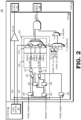
- FIG. 2 illustrates a block diagram of a portion 200 of the processor core 114 of FIG. 1 in accordance with some embodiments.
- the portion 200 includes a clock divider circuit 202 which further includes a duty cycle adjuster 204 and a transmission gate multiplexer (mux) 210 in which a clock signal (Clkln) acts as a select signal that picks between two enable inputs.
- the clock divider circuit 202 includes latches 212, 222, 232, OR gates 242, 252, AND gates 262, 272, the duty cycle adjuster 204, and the transmission gate multiplexer (mux) 210. As discussed above with regard to FIG.
- the processor core 114 receives P-state clock frequencies (e.g., Clkln and ClkX) from the level shifter 142 of the L3 cache 140.
- Core clock (CCLK) enable signals (CKGEN_EnableA and CKGEN_EnableB) are driven from rising edge flops in the CKGEN (e.g., CKGEN 174 of FIG. 1 ) to meet setup time to rising edge flops in the DFS 164.
- Latches 206 and 208 of the DFS 164 receive and act on the CKGEN_EnableA and CKGEN_EnableB signals, respectively.
- the latch 206 includes a data input to receive the enable signal CKGEN_EnableA, a clock input to receive the clock signal Clkln, and an output.
- the latch 208 includes a data input to receive the enable signal CKGEN_EnableB, a clock input to receive the clock signal Clkln, and an output.
- the stretch assertion signal (i.e., StretchEn) is asserted upon detection of a power supply droop to enable clock stretching that picks between two stretch-enable EN signals (i.e., Str_ENA, Str_ENB). Any clock divide in 0.5 increments (e.g., 1.0, 1.5, 2.0, 2.5, etc.) can be achieved by modulating the EN bits.
- StrEn assertion overrides the CKGEN_EnableA and CKGEN_EnableB bits to force a 100% stretch for a single cycle.
- the clock divider circuit 202 supports clock ramp up/ramp down during CC6 Entry/Exit and scan shift reset entry/exit by performing clock divides with 0.5 granularity (1.0, 1.5, 2.0, 2.5, etc.). Accordingly, clock divider circuit 202 configures a transmission gate mux 210 in which the clock (i.e., ClkX) acts as a select which picks between two EN inputs (and associated logic controlling the two EN inputs). The slow ramp up/down of clock frequency enabled by the clock divider circuit 202 provides di/dt mitigation.
- the clock i.e., ClkX
- the slow ramp up/down of clock frequency enabled by the clock divider circuit 202 provides di/dt mitigation.
- the clock divider circuit 202 also includes a duty cycle adjuster 204 which provides the final EN inputs to the mux 210.
- Rise and fall edge rate at the output i.e., ClkOutX
- pFET p-channel field-effect transistor
- nFET n-channel field-effect transistor
- Independent control of pFET and nFET strength using Fuse/JTAG bits i.e., ENN[6:0], ENP[6:0]
- Positioning the duty cycle adjuster 204 within the clock divider circuit 202 avoids adding stages to support duty cycle adjusting, thereby reducing jitter.
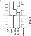
- FIG. 3 illustrates a waveform diagram 300 of various clock signals in accordance with some embodiments.
- the waveform diagram 300 shows waveforms for clock divide by 1, followed by stretch.
- the StrEn signal is in a negated state, indicating that no voltage droop has been detected at the processor core 114.
- the frequency of the clock signal output ClkOutX is determined only by the clock divider circuit 202, wherein it generates the ClkOutX to have a frequency equal to the frequency of the input clock signal (i.e., CLK) divided by 1.
- the StrEn signal is asserted, indicating a voltage droop at the processor core 114.
- the frequency of ClkOutX is controlled by the two enable (EN) inputs (i.e., Str_ENA, Str_ENB).
- the clock divider circuit 202 reduces the frequency of ClkOutX relative to its frequency prior to time 304 by 100%, thereby adjusting for the voltage droop.
- ClkOutX returns to the same frequency as CLK even though StrEn may remain high.
- the CLK input is stretched by other means not included in this disclosure if StrEn remains high. In this way, ClkOutX is stretched faster than may be provided for in systems that stretches CLK.
- FIG. 4 illustrates a flow diagram of a method 400 of adjusting a frequency of a clock signal in response to detecting a voltage droop at a processor core in accordance with at least one embodiment.
- the method 400 is described with respect to an example implementation at the processor core 114 of FIG. 1 and clock divider circuit 202 of FIG. 2 .
- the level shifter 142 at the L3 cache 140 provides a nominal frequency setting for the clock signal ClkX.
- the CKGEN 174 drives CCLK enable signals (CKGEN_EnableA and CKGEN_EnableB) to meet setup time to rising edge flops in the DFS 164.
- a droop detector circuit generates the stretch assertion signal StretchEn for setting the ClkX clock signal to a lower frequency relative to its nominal frequency.
- the droop detector circuit monitors the voltage at one or more points of the processor core 114 to identify whether a voltage droop is present. If not, the droop detector circuit maintains the StretchEn signal in a negated state. In response, the method flow moves to block 410, and the DFS 164 generates an output clock signal based on the CCLK enable signals (i.e., CKGEN_EnableA and CKGEN_EnableB). The method flow then returns to block 408 as the droop detector circuit continues to monitor the voltage at processor core 114.
- the CCLK enable signals i.e., CKGEN_EnableA and CKGEN_EnableB
- the droop detector circuit in response to detecting a voltage droop the droop detector circuit asserts the StretchEn signal.
- the method flow moves to block 412 and the clock divide circuit 202 generates an output clock signal based on the two stretch-enable EN signals (i.e., Str_ENA, Str_ENB), thus generating an output clock signal at a slower frequency.
- the input clock signal can be divided with a granularity of 0.5 increments (e.g., 1.0, 1.5, 2.0, 2.5, etc.) by modulating the EN bits.
- StretchEn assertion overrides the EN bits to force a 100% stretch for a single cycle.
- clock divider circuit 202 operates as a transmission gate mux in which the clock (i.e., ClkX) acts as a select which picks between two EN inputs (and associated logic controlling the two EN inputs).
- the slow ramp up/down of clock frequency enabled by the clock divider circuit 202 provides dl/dT mitigation.
- the method flow proceeds to blocks 414 and 416 and the droop detector circuit monitors whether the voltage at the processor core 114 has returned to its nominal level or range. If not, the method returns to block 414 as the clock divider circuit 202 maintains the output clock signal ClkOut on the Clkln frequency (Clkln may itself be stretched by a mechanism outside of clock divider circuit 202 after the initial clock stretch from block 412 has had effect). If, at block 416, the droop detector circuit identifies that the monitored voltage has returned to its nominal level or range, and the method flow proceeds to block 410, where the droop detector circuit negates the StretchEn signal, causing the DFS 164 to return to generating the output clock signal at its nominal input frequency.
- certain aspects of the techniques described above may implemented by one or more processors of a processing system executing software.
- the software includes one or more sets of executable instructions stored or otherwise tangibly embodied on a non-transitory computer readable storage medium.
- the software can include the instructions and certain data that, when executed by the one or more processors, manipulate the one or more processors to perform one or more aspects of the techniques described above.
- the non-transitory computer readable storage medium can include, for example, a magnetic or optical disk storage device, solid state storage devices such as Flash memory, a cache, random access memory (RAM) or other non-volatile memory device or devices, and the like.
- the executable instructions stored on the non-transitory computer readable storage medium may be in source code, assembly language code, object code, or other instruction format that is interpreted or otherwise executable by one or more processors.
Landscapes
- Engineering & Computer Science (AREA)
- Theoretical Computer Science (AREA)
- General Engineering & Computer Science (AREA)
- Physics & Mathematics (AREA)
- General Physics & Mathematics (AREA)
- Power Sources (AREA)
- Microcomputers (AREA)
- Computer Hardware Design (AREA)
- Computing Systems (AREA)
Applications Claiming Priority (2)
| Application Number | Priority Date | Filing Date | Title |
|---|---|---|---|
| US15/441,613 US10303200B2 (en) | 2017-02-24 | 2017-02-24 | Clock divider device and methods thereof |
| PCT/US2018/018718 WO2018156485A1 (en) | 2017-02-24 | 2018-02-20 | Clock divider device and methods thereof |
Publications (3)
| Publication Number | Publication Date |
|---|---|
| EP3586214A1 EP3586214A1 (en) | 2020-01-01 |
| EP3586214A4 EP3586214A4 (en) | 2020-12-16 |
| EP3586214B1 true EP3586214B1 (en) | 2023-05-31 |
Family
ID=63246265
Family Applications (1)
| Application Number | Title | Priority Date | Filing Date |
|---|---|---|---|
| EP18756852.2A Active EP3586214B1 (en) | 2017-02-24 | 2018-02-20 | Clock divider device and methods thereof |
Country Status (6)
Families Citing this family (6)
| Publication number | Priority date | Publication date | Assignee | Title |
|---|---|---|---|---|
| GB2590660B (en) * | 2019-12-23 | 2022-01-05 | Graphcore Ltd | Reactive droop limiter |
| US11895588B2 (en) * | 2020-08-05 | 2024-02-06 | Analog Devices, Inc. | Timing precision maintenance with reduced power during system sleep |
| US12019499B2 (en) * | 2021-12-16 | 2024-06-25 | Advanced Micro Devices, Inc. | System and method to reduce power down entry and exit latency |
| KR102756169B1 (ko) | 2022-07-08 | 2025-01-15 | 창신 메모리 테크놀로지즈 아이엔씨 | 메모리, 제어 장치, 클럭 처리 방법과 전자 기기 |
| CN117409828A (zh) * | 2022-07-08 | 2024-01-16 | 长鑫存储技术有限公司 | 一种存储器、控制装置、时钟处理方法和电子设备 |
| US12061509B2 (en) * | 2022-12-15 | 2024-08-13 | International Business Machines Corporation | Voltage droop and overshoot management using non-linear slope detection |
Family Cites Families (28)
| Publication number | Priority date | Publication date | Assignee | Title |
|---|---|---|---|---|
| JP2959657B2 (ja) | 1993-05-13 | 1999-10-06 | キヤノン株式会社 | 電子機器 |
| JP2000207381A (ja) | 1999-01-20 | 2000-07-28 | Mitsubishi Electric Corp | マイクロコンピュ―タのリセット装置 |
| US7114038B2 (en) | 2001-12-28 | 2006-09-26 | Intel Corporation | Method and apparatus for communicating between integrated circuits in a low power mode |
| US6922111B2 (en) * | 2002-12-20 | 2005-07-26 | Intel Corporation | Adaptive frequency clock signal |
| US6882238B2 (en) * | 2003-03-21 | 2005-04-19 | Intel Corporation | Method and apparatus for detecting on-die voltage variations |
| US7007188B1 (en) | 2003-04-29 | 2006-02-28 | Advanced Micro Devices, Inc. | Precision bypass clock for high speed testing of a data processor |
| US7225349B2 (en) | 2003-07-25 | 2007-05-29 | Intel Corporation | Power supply voltage droop compensated clock modulation for microprocessors |
| US7076679B2 (en) | 2003-10-06 | 2006-07-11 | Hewlett-Packard Development Company, L.P. | System and method for synchronizing multiple variable-frequency clock generators |
| DE10354215B4 (de) | 2003-11-20 | 2010-02-25 | Infineon Technologies Ag | Taktregulierungsvorrichtung sowie Schaltungsanordnung |
| WO2006091826A2 (en) * | 2005-02-23 | 2006-08-31 | Multigig, Inc. | Low noise divider |
| JP4492394B2 (ja) | 2005-03-08 | 2010-06-30 | 株式会社デンソー | マイクロコンピュータ |
| US8037340B2 (en) | 2007-11-28 | 2011-10-11 | International Business Machines Corporation | Apparatus and method for micro performance tuning of a clocked digital system |
| US7570122B2 (en) * | 2007-12-22 | 2009-08-04 | Broadcom Corporation | Low voltage LOGEN |
| DE102008061034B3 (de) | 2008-12-08 | 2010-04-08 | Fujitsu Siemens Computers Gmbh | Anordnung umfassend wenigstens zwei Stromversorgungseinheiten und wenigstens eine Strom verbrauchende Komponente, Computersystem sowie Verfahren zur Steuerung einer Anordnung |
| US8433944B2 (en) * | 2010-04-12 | 2013-04-30 | Qualcomm Incorporated | Clock divider system and method with incremental adjustment steps while controlling tolerance in clock duty cycle |
| US8384435B2 (en) * | 2011-01-05 | 2013-02-26 | Texas Instruments Incorporated | Clock switching circuit with priority multiplexer |
| US20120187991A1 (en) * | 2011-01-25 | 2012-07-26 | Advanced Micro Devices, Inc. | Clock stretcher for voltage droop mitigation |
| US8937511B2 (en) | 2011-11-22 | 2015-01-20 | Marvell World Trade Ltd. | Frequency scaling of variable speed systems for fast response and power reduction |
| WO2013095633A1 (en) | 2011-12-23 | 2013-06-27 | Intel Corporation | Characterization of within-die variations of many-core processors |
| US9065440B2 (en) * | 2013-01-30 | 2015-06-23 | Altera Corporation | Bypassable clocked storage circuitry for dynamic voltage-frequency scaling |
| US10020931B2 (en) * | 2013-03-07 | 2018-07-10 | Intel Corporation | Apparatus for dynamically adapting a clock generator with respect to changes in power supply |
| US8933737B1 (en) * | 2013-06-28 | 2015-01-13 | Stmicroelectronics International N.V. | System and method for variable frequency clock generation |
| CN105375917B (zh) * | 2013-12-13 | 2019-01-29 | 马维尔国际有限公司 | 分频器 |
| US9753525B2 (en) | 2014-12-23 | 2017-09-05 | Intel Corporation | Systems and methods for core droop mitigation based on license state |
| US9778676B2 (en) | 2015-08-03 | 2017-10-03 | Qualcomm Incorporated | Power distribution network (PDN) droop/overshoot mitigation in dynamic frequency scaling |
| US9798376B2 (en) * | 2015-08-03 | 2017-10-24 | Qualcomm Incorporated | Power distribution network (PDN) droop/overshoot mitigation |
| US9915968B2 (en) * | 2016-04-19 | 2018-03-13 | Qualcomm Incorporated | Systems and methods for adaptive clock design |
| US10148258B2 (en) * | 2016-09-28 | 2018-12-04 | Mellanox Technologies, Ltd. | Power supply voltage monitoring and high-resolution adaptive clock stretching circuit |
-
2017
- 2017-02-24 US US15/441,613 patent/US10303200B2/en active Active
-
2018
- 2018-02-20 KR KR1020197023013A patent/KR102306084B1/ko active Active
- 2018-02-20 JP JP2019546135A patent/JP6905596B2/ja active Active
- 2018-02-20 CN CN201880008576.9A patent/CN110226148B/zh active Active
- 2018-02-20 WO PCT/US2018/018718 patent/WO2018156485A1/en unknown
- 2018-02-20 EP EP18756852.2A patent/EP3586214B1/en active Active
Also Published As
| Publication number | Publication date |
|---|---|
| EP3586214A1 (en) | 2020-01-01 |
| US20180246557A1 (en) | 2018-08-30 |
| CN110226148B (zh) | 2021-04-09 |
| KR102306084B1 (ko) | 2021-09-28 |
| EP3586214A4 (en) | 2020-12-16 |
| US10303200B2 (en) | 2019-05-28 |
| KR20190113809A (ko) | 2019-10-08 |
| CN110226148A (zh) | 2019-09-10 |
| JP6905596B2 (ja) | 2021-07-21 |
| JP2020510253A (ja) | 2020-04-02 |
| WO2018156485A1 (en) | 2018-08-30 |
Similar Documents
| Publication | Publication Date | Title |
|---|---|---|
| EP3586214B1 (en) | Clock divider device and methods thereof | |
| US10642336B2 (en) | Clock adjustment for voltage droop | |
| US9703313B2 (en) | Peripheral clock management | |
| US7051227B2 (en) | Method and apparatus for reducing clock frequency during low workload periods | |
| US9223383B2 (en) | Guardband reduction for multi-core data processor | |
| US8438416B2 (en) | Function based dynamic power control | |
| CN108763129B (zh) | 具有相同的指令集架构(isa)的非对称性能多核架构 | |
| US8769332B2 (en) | Regional clock gating and dithering | |
| US5935253A (en) | Method and apparatus for powering down an integrated circuit having a core that operates at a speed greater than the bus frequency | |
| EP3198438B1 (en) | Hardware apparatus and method for multiple processors dynamic asymmetric and symmetric mode switching | |
| CN110573991B (zh) | 架构状态保留 | |
| US10928882B2 (en) | Low cost, low power high performance SMP/ASMP multiple-processor system | |
| JP7654908B2 (ja) | デジタル周波数ロックループのドループ検出及び制御 | |
| US11973504B2 (en) | Multi-reset and multi-clock synchronizer, and synchronous multi-cycle reset synchronization circuit | |
| CN108139791B (zh) | 功率监控的cpu功率网设计 | |
| KR100958966B1 (ko) | 클럭 분배 도메인들로의 클럭 분배 순서 제어 | |
| CN111356966B (zh) | 基于动态时钟和电压缩放定时对中央处理单元存储器分组以使用阵列功率复用器提高动态/泄漏功率 | |
| TWI849227B (zh) | 時脈交叉先進先出(fifo)狀態斂聚式同步器 | |
| EP3270257B1 (en) | Clock adjustment for voltage droop | |
| US20160216756A1 (en) | Power management in computing devices |
Legal Events
| Date | Code | Title | Description |
|---|---|---|---|
| STAA | Information on the status of an ep patent application or granted ep patent |
Free format text: STATUS: THE INTERNATIONAL PUBLICATION HAS BEEN MADE |
|
| PUAI | Public reference made under article 153(3) epc to a published international application that has entered the european phase |
Free format text: ORIGINAL CODE: 0009012 |
|
| STAA | Information on the status of an ep patent application or granted ep patent |
Free format text: STATUS: REQUEST FOR EXAMINATION WAS MADE |
|
| 17P | Request for examination filed |
Effective date: 20190827 |
|
| AK | Designated contracting states |
Kind code of ref document: A1 Designated state(s): AL AT BE BG CH CY CZ DE DK EE ES FI FR GB GR HR HU IE IS IT LI LT LU LV MC MK MT NL NO PL PT RO RS SE SI SK SM TR |
|
| AX | Request for extension of the european patent |
Extension state: BA ME |
|
| DAV | Request for validation of the european patent (deleted) | ||
| DAX | Request for extension of the european patent (deleted) | ||
| REG | Reference to a national code |
Ref country code: DE Ref legal event code: R079 Ref document number: 602018050469 Country of ref document: DE Free format text: PREVIOUS MAIN CLASS: G06F0001100000 Ipc: G06F0001080000 |
|
| A4 | Supplementary search report drawn up and despatched |
Effective date: 20201116 |
|
| RIC1 | Information provided on ipc code assigned before grant |
Ipc: G06F 1/08 20060101AFI20201110BHEP Ipc: G06F 1/324 20190101ALI20201110BHEP Ipc: G06F 1/3206 20190101ALI20201110BHEP Ipc: G06F 1/30 20060101ALI20201110BHEP |
|
| GRAP | Despatch of communication of intention to grant a patent |
Free format text: ORIGINAL CODE: EPIDOSNIGR1 |
|
| STAA | Information on the status of an ep patent application or granted ep patent |
Free format text: STATUS: GRANT OF PATENT IS INTENDED |
|
| INTG | Intention to grant announced |
Effective date: 20220721 |
|
| RIN1 | Information on inventor provided before grant (corrected) |
Inventor name: MITTAL, VIBHOR Inventor name: KOMMRUSCH, STEVEN Inventor name: JOHN, DEEPESH |
|
| GRAJ | Information related to disapproval of communication of intention to grant by the applicant or resumption of examination proceedings by the epo deleted |
Free format text: ORIGINAL CODE: EPIDOSDIGR1 |
|
| STAA | Information on the status of an ep patent application or granted ep patent |
Free format text: STATUS: REQUEST FOR EXAMINATION WAS MADE |
|
| GRAP | Despatch of communication of intention to grant a patent |
Free format text: ORIGINAL CODE: EPIDOSNIGR1 |
|
| STAA | Information on the status of an ep patent application or granted ep patent |
Free format text: STATUS: GRANT OF PATENT IS INTENDED |
|
| INTC | Intention to grant announced (deleted) | ||
| INTG | Intention to grant announced |
Effective date: 20221222 |
|
| GRAS | Grant fee paid |
Free format text: ORIGINAL CODE: EPIDOSNIGR3 |
|
| GRAA | (expected) grant |
Free format text: ORIGINAL CODE: 0009210 |
|
| STAA | Information on the status of an ep patent application or granted ep patent |
Free format text: STATUS: THE PATENT HAS BEEN GRANTED |
|
| AK | Designated contracting states |
Kind code of ref document: B1 Designated state(s): AL AT BE BG CH CY CZ DE DK EE ES FI FR GB GR HR HU IE IS IT LI LT LU LV MC MK MT NL NO PL PT RO RS SE SI SK SM TR |
|
| REG | Reference to a national code |
Ref country code: GB Ref legal event code: FG4D Ref country code: CH Ref legal event code: EP |
|
| REG | Reference to a national code |
Ref country code: AT Ref legal event code: REF Ref document number: 1571302 Country of ref document: AT Kind code of ref document: T Effective date: 20230615 Ref country code: DE Ref legal event code: R096 Ref document number: 602018050469 Country of ref document: DE |
|
| REG | Reference to a national code |
Ref country code: IE Ref legal event code: FG4D |
|
| P01 | Opt-out of the competence of the unified patent court (upc) registered |
Effective date: 20230530 |
|
| REG | Reference to a national code |
Ref country code: LT Ref legal event code: MG9D |
|
| REG | Reference to a national code |
Ref country code: NL Ref legal event code: MP Effective date: 20230531 |
|
| REG | Reference to a national code |
Ref country code: AT Ref legal event code: MK05 Ref document number: 1571302 Country of ref document: AT Kind code of ref document: T Effective date: 20230531 |
|
| PG25 | Lapsed in a contracting state [announced via postgrant information from national office to epo] |
Ref country code: SE Free format text: LAPSE BECAUSE OF FAILURE TO SUBMIT A TRANSLATION OF THE DESCRIPTION OR TO PAY THE FEE WITHIN THE PRESCRIBED TIME-LIMIT Effective date: 20230531 Ref country code: NO Free format text: LAPSE BECAUSE OF FAILURE TO SUBMIT A TRANSLATION OF THE DESCRIPTION OR TO PAY THE FEE WITHIN THE PRESCRIBED TIME-LIMIT Effective date: 20230831 Ref country code: ES Free format text: LAPSE BECAUSE OF FAILURE TO SUBMIT A TRANSLATION OF THE DESCRIPTION OR TO PAY THE FEE WITHIN THE PRESCRIBED TIME-LIMIT Effective date: 20230531 Ref country code: AT Free format text: LAPSE BECAUSE OF FAILURE TO SUBMIT A TRANSLATION OF THE DESCRIPTION OR TO PAY THE FEE WITHIN THE PRESCRIBED TIME-LIMIT Effective date: 20230531 |
|
| PG25 | Lapsed in a contracting state [announced via postgrant information from national office to epo] |
Ref country code: RS Free format text: LAPSE BECAUSE OF FAILURE TO SUBMIT A TRANSLATION OF THE DESCRIPTION OR TO PAY THE FEE WITHIN THE PRESCRIBED TIME-LIMIT Effective date: 20230531 Ref country code: PL Free format text: LAPSE BECAUSE OF FAILURE TO SUBMIT A TRANSLATION OF THE DESCRIPTION OR TO PAY THE FEE WITHIN THE PRESCRIBED TIME-LIMIT Effective date: 20230531 Ref country code: NL Free format text: LAPSE BECAUSE OF FAILURE TO SUBMIT A TRANSLATION OF THE DESCRIPTION OR TO PAY THE FEE WITHIN THE PRESCRIBED TIME-LIMIT Effective date: 20230531 Ref country code: LV Free format text: LAPSE BECAUSE OF FAILURE TO SUBMIT A TRANSLATION OF THE DESCRIPTION OR TO PAY THE FEE WITHIN THE PRESCRIBED TIME-LIMIT Effective date: 20230531 Ref country code: LT Free format text: LAPSE BECAUSE OF FAILURE TO SUBMIT A TRANSLATION OF THE DESCRIPTION OR TO PAY THE FEE WITHIN THE PRESCRIBED TIME-LIMIT Effective date: 20230531 Ref country code: IS Free format text: LAPSE BECAUSE OF FAILURE TO SUBMIT A TRANSLATION OF THE DESCRIPTION OR TO PAY THE FEE WITHIN THE PRESCRIBED TIME-LIMIT Effective date: 20230930 Ref country code: HR Free format text: LAPSE BECAUSE OF FAILURE TO SUBMIT A TRANSLATION OF THE DESCRIPTION OR TO PAY THE FEE WITHIN THE PRESCRIBED TIME-LIMIT Effective date: 20230531 Ref country code: GR Free format text: LAPSE BECAUSE OF FAILURE TO SUBMIT A TRANSLATION OF THE DESCRIPTION OR TO PAY THE FEE WITHIN THE PRESCRIBED TIME-LIMIT Effective date: 20230901 |
|
| PG25 | Lapsed in a contracting state [announced via postgrant information from national office to epo] |
Ref country code: FI Free format text: LAPSE BECAUSE OF FAILURE TO SUBMIT A TRANSLATION OF THE DESCRIPTION OR TO PAY THE FEE WITHIN THE PRESCRIBED TIME-LIMIT Effective date: 20230531 |
|
| PG25 | Lapsed in a contracting state [announced via postgrant information from national office to epo] |
Ref country code: SK Free format text: LAPSE BECAUSE OF FAILURE TO SUBMIT A TRANSLATION OF THE DESCRIPTION OR TO PAY THE FEE WITHIN THE PRESCRIBED TIME-LIMIT Effective date: 20230531 |
|
| PG25 | Lapsed in a contracting state [announced via postgrant information from national office to epo] |
Ref country code: SM Free format text: LAPSE BECAUSE OF FAILURE TO SUBMIT A TRANSLATION OF THE DESCRIPTION OR TO PAY THE FEE WITHIN THE PRESCRIBED TIME-LIMIT Effective date: 20230531 Ref country code: SK Free format text: LAPSE BECAUSE OF FAILURE TO SUBMIT A TRANSLATION OF THE DESCRIPTION OR TO PAY THE FEE WITHIN THE PRESCRIBED TIME-LIMIT Effective date: 20230531 Ref country code: RO Free format text: LAPSE BECAUSE OF FAILURE TO SUBMIT A TRANSLATION OF THE DESCRIPTION OR TO PAY THE FEE WITHIN THE PRESCRIBED TIME-LIMIT Effective date: 20230531 Ref country code: PT Free format text: LAPSE BECAUSE OF FAILURE TO SUBMIT A TRANSLATION OF THE DESCRIPTION OR TO PAY THE FEE WITHIN THE PRESCRIBED TIME-LIMIT Effective date: 20231002 Ref country code: EE Free format text: LAPSE BECAUSE OF FAILURE TO SUBMIT A TRANSLATION OF THE DESCRIPTION OR TO PAY THE FEE WITHIN THE PRESCRIBED TIME-LIMIT Effective date: 20230531 Ref country code: DK Free format text: LAPSE BECAUSE OF FAILURE TO SUBMIT A TRANSLATION OF THE DESCRIPTION OR TO PAY THE FEE WITHIN THE PRESCRIBED TIME-LIMIT Effective date: 20230531 Ref country code: CZ Free format text: LAPSE BECAUSE OF FAILURE TO SUBMIT A TRANSLATION OF THE DESCRIPTION OR TO PAY THE FEE WITHIN THE PRESCRIBED TIME-LIMIT Effective date: 20230531 |
|
| REG | Reference to a national code |
Ref country code: DE Ref legal event code: R097 Ref document number: 602018050469 Country of ref document: DE |
|
| PLBE | No opposition filed within time limit |
Free format text: ORIGINAL CODE: 0009261 |
|
| STAA | Information on the status of an ep patent application or granted ep patent |
Free format text: STATUS: NO OPPOSITION FILED WITHIN TIME LIMIT |
|
| PG25 | Lapsed in a contracting state [announced via postgrant information from national office to epo] |
Ref country code: SI Free format text: LAPSE BECAUSE OF FAILURE TO SUBMIT A TRANSLATION OF THE DESCRIPTION OR TO PAY THE FEE WITHIN THE PRESCRIBED TIME-LIMIT Effective date: 20230531 |
|
| 26N | No opposition filed |
Effective date: 20240301 |
|
| PG25 | Lapsed in a contracting state [announced via postgrant information from national office to epo] |
Ref country code: SI Free format text: LAPSE BECAUSE OF FAILURE TO SUBMIT A TRANSLATION OF THE DESCRIPTION OR TO PAY THE FEE WITHIN THE PRESCRIBED TIME-LIMIT Effective date: 20230531 Ref country code: IT Free format text: LAPSE BECAUSE OF FAILURE TO SUBMIT A TRANSLATION OF THE DESCRIPTION OR TO PAY THE FEE WITHIN THE PRESCRIBED TIME-LIMIT Effective date: 20230531 |
|
| PG25 | Lapsed in a contracting state [announced via postgrant information from national office to epo] |
Ref country code: MC Free format text: LAPSE BECAUSE OF FAILURE TO SUBMIT A TRANSLATION OF THE DESCRIPTION OR TO PAY THE FEE WITHIN THE PRESCRIBED TIME-LIMIT Effective date: 20230531 |
|
| REG | Reference to a national code |
Ref country code: CH Ref legal event code: PL |
|
| PG25 | Lapsed in a contracting state [announced via postgrant information from national office to epo] |
Ref country code: LU Free format text: LAPSE BECAUSE OF NON-PAYMENT OF DUE FEES Effective date: 20240220 |
|
| PG25 | Lapsed in a contracting state [announced via postgrant information from national office to epo] |
Ref country code: CH Free format text: LAPSE BECAUSE OF NON-PAYMENT OF DUE FEES Effective date: 20240229 |
|
| PG25 | Lapsed in a contracting state [announced via postgrant information from national office to epo] |
Ref country code: LU Free format text: LAPSE BECAUSE OF NON-PAYMENT OF DUE FEES Effective date: 20240220 Ref country code: CH Free format text: LAPSE BECAUSE OF NON-PAYMENT OF DUE FEES Effective date: 20240229 |
|
| PG25 | Lapsed in a contracting state [announced via postgrant information from national office to epo] |
Ref country code: BG Free format text: LAPSE BECAUSE OF FAILURE TO SUBMIT A TRANSLATION OF THE DESCRIPTION OR TO PAY THE FEE WITHIN THE PRESCRIBED TIME-LIMIT Effective date: 20230531 |
|
| PG25 | Lapsed in a contracting state [announced via postgrant information from national office to epo] |
Ref country code: BG Free format text: LAPSE BECAUSE OF FAILURE TO SUBMIT A TRANSLATION OF THE DESCRIPTION OR TO PAY THE FEE WITHIN THE PRESCRIBED TIME-LIMIT Effective date: 20230531 |
|
| REG | Reference to a national code |
Ref country code: BE Ref legal event code: MM Effective date: 20240229 |
|
| PG25 | Lapsed in a contracting state [announced via postgrant information from national office to epo] |
Ref country code: BE Free format text: LAPSE BECAUSE OF NON-PAYMENT OF DUE FEES Effective date: 20240229 |
|
| PG25 | Lapsed in a contracting state [announced via postgrant information from national office to epo] |
Ref country code: FR Free format text: LAPSE BECAUSE OF NON-PAYMENT OF DUE FEES Effective date: 20240229 |
|
| PG25 | Lapsed in a contracting state [announced via postgrant information from national office to epo] |
Ref country code: IE Free format text: LAPSE BECAUSE OF NON-PAYMENT OF DUE FEES Effective date: 20240220 |
|
| PG25 | Lapsed in a contracting state [announced via postgrant information from national office to epo] |
Ref country code: IE Free format text: LAPSE BECAUSE OF NON-PAYMENT OF DUE FEES Effective date: 20240220 Ref country code: FR Free format text: LAPSE BECAUSE OF NON-PAYMENT OF DUE FEES Effective date: 20240229 Ref country code: BE Free format text: LAPSE BECAUSE OF NON-PAYMENT OF DUE FEES Effective date: 20240229 |
|
| PGFP | Annual fee paid to national office [announced via postgrant information from national office to epo] |
Ref country code: DE Payment date: 20250128 Year of fee payment: 8 |
|
| PGFP | Annual fee paid to national office [announced via postgrant information from national office to epo] |
Ref country code: GB Payment date: 20250210 Year of fee payment: 8 |
|
| PG25 | Lapsed in a contracting state [announced via postgrant information from national office to epo] |
Ref country code: CY Free format text: LAPSE BECAUSE OF FAILURE TO SUBMIT A TRANSLATION OF THE DESCRIPTION OR TO PAY THE FEE WITHIN THE PRESCRIBED TIME-LIMIT; INVALID AB INITIO Effective date: 20180220 |
|
| PG25 | Lapsed in a contracting state [announced via postgrant information from national office to epo] |
Ref country code: HU Free format text: LAPSE BECAUSE OF FAILURE TO SUBMIT A TRANSLATION OF THE DESCRIPTION OR TO PAY THE FEE WITHIN THE PRESCRIBED TIME-LIMIT; INVALID AB INITIO Effective date: 20180220 |