EP3582260A2 - Elektronisches gehäuse für kommunikationsanwendungen mit hohen datenraten - Google Patents
Elektronisches gehäuse für kommunikationsanwendungen mit hohen datenraten Download PDFInfo
- Publication number
- EP3582260A2 EP3582260A2 EP19172944.1A EP19172944A EP3582260A2 EP 3582260 A2 EP3582260 A2 EP 3582260A2 EP 19172944 A EP19172944 A EP 19172944A EP 3582260 A2 EP3582260 A2 EP 3582260A2
- Authority
- EP
- European Patent Office
- Prior art keywords
- package substrate
- package
- interface circuit
- speed interface
- circuit die
- Prior art date
- Legal status (The legal status is an assumption and is not a legal conclusion. Google has not performed a legal analysis and makes no representation as to the accuracy of the status listed.)
- Withdrawn
Links
Images

Classifications
-
- H—ELECTRICITY
- H10—SEMICONDUCTOR DEVICES; ELECTRIC SOLID-STATE DEVICES NOT OTHERWISE PROVIDED FOR
- H10W—GENERIC PACKAGES, INTERCONNECTIONS, CONNECTORS OR OTHER CONSTRUCTIONAL DETAILS OF DEVICES COVERED BY CLASS H10
- H10W90/00—Package configurations
- H10W90/401—Package configurations characterised by multiple insulating or insulated package substrates, interposers or RDLs
-
- H—ELECTRICITY
- H10—SEMICONDUCTOR DEVICES; ELECTRIC SOLID-STATE DEVICES NOT OTHERWISE PROVIDED FOR
- H10W—GENERIC PACKAGES, INTERCONNECTIONS, CONNECTORS OR OTHER CONSTRUCTIONAL DETAILS OF DEVICES COVERED BY CLASS H10
- H10W20/00—Interconnections in chips, wafers or substrates
- H10W20/40—Interconnections external to wafers or substrates, e.g. back-end-of-line [BEOL] metallisations or vias connecting to gate electrodes
- H10W20/41—Interconnections external to wafers or substrates, e.g. back-end-of-line [BEOL] metallisations or vias connecting to gate electrodes characterised by their conductive parts
- H10W20/42—Vias, e.g. via plugs
-
- H—ELECTRICITY
- H10—SEMICONDUCTOR DEVICES; ELECTRIC SOLID-STATE DEVICES NOT OTHERWISE PROVIDED FOR
- H10W—GENERIC PACKAGES, INTERCONNECTIONS, CONNECTORS OR OTHER CONSTRUCTIONAL DETAILS OF DEVICES COVERED BY CLASS H10
- H10W20/00—Interconnections in chips, wafers or substrates
- H10W20/40—Interconnections external to wafers or substrates, e.g. back-end-of-line [BEOL] metallisations or vias connecting to gate electrodes
- H10W20/41—Interconnections external to wafers or substrates, e.g. back-end-of-line [BEOL] metallisations or vias connecting to gate electrodes characterised by their conductive parts
- H10W20/435—Cross-sectional shapes or dispositions of interconnections
-
- H—ELECTRICITY
- H10—SEMICONDUCTOR DEVICES; ELECTRIC SOLID-STATE DEVICES NOT OTHERWISE PROVIDED FOR
- H10W—GENERIC PACKAGES, INTERCONNECTIONS, CONNECTORS OR OTHER CONSTRUCTIONAL DETAILS OF DEVICES COVERED BY CLASS H10
- H10W70/00—Package substrates; Interposers; Redistribution layers [RDL]
- H10W70/01—Manufacture or treatment
- H10W70/05—Manufacture or treatment of insulating or insulated package substrates, or of interposers, or of redistribution layers
- H10W70/08—Manufacture or treatment of insulating or insulated package substrates, or of interposers, or of redistribution layers by depositing layers on the chip or wafer, e.g. "chip-first" RDLs
- H10W70/09—Manufacture or treatment of insulating or insulated package substrates, or of interposers, or of redistribution layers by depositing layers on the chip or wafer, e.g. "chip-first" RDLs extending onto an encapsulation that laterally surrounds the chip or wafer, e.g. fan-out wafer level package [FOWLP] RDLs
-
- H—ELECTRICITY
- H10—SEMICONDUCTOR DEVICES; ELECTRIC SOLID-STATE DEVICES NOT OTHERWISE PROVIDED FOR
- H10W—GENERIC PACKAGES, INTERCONNECTIONS, CONNECTORS OR OTHER CONSTRUCTIONAL DETAILS OF DEVICES COVERED BY CLASS H10
- H10W70/00—Package substrates; Interposers; Redistribution layers [RDL]
- H10W70/60—Insulating or insulated package substrates; Interposers; Redistribution layers
-
- H—ELECTRICITY
- H10—SEMICONDUCTOR DEVICES; ELECTRIC SOLID-STATE DEVICES NOT OTHERWISE PROVIDED FOR
- H10W—GENERIC PACKAGES, INTERCONNECTIONS, CONNECTORS OR OTHER CONSTRUCTIONAL DETAILS OF DEVICES COVERED BY CLASS H10
- H10W70/00—Package substrates; Interposers; Redistribution layers [RDL]
- H10W70/60—Insulating or insulated package substrates; Interposers; Redistribution layers
- H10W70/611—Insulating or insulated package substrates; Interposers; Redistribution layers for connecting multiple chips together
-
- H—ELECTRICITY
- H10—SEMICONDUCTOR DEVICES; ELECTRIC SOLID-STATE DEVICES NOT OTHERWISE PROVIDED FOR
- H10W—GENERIC PACKAGES, INTERCONNECTIONS, CONNECTORS OR OTHER CONSTRUCTIONAL DETAILS OF DEVICES COVERED BY CLASS H10
- H10W72/00—Interconnections or connectors in packages
- H10W72/20—Bump connectors, e.g. solder bumps or copper pillars; Dummy bumps; Thermal bumps
-
- H—ELECTRICITY
- H10—SEMICONDUCTOR DEVICES; ELECTRIC SOLID-STATE DEVICES NOT OTHERWISE PROVIDED FOR
- H10W—GENERIC PACKAGES, INTERCONNECTIONS, CONNECTORS OR OTHER CONSTRUCTIONAL DETAILS OF DEVICES COVERED BY CLASS H10
- H10W72/00—Interconnections or connectors in packages
- H10W72/90—Bond pads, in general
-
- H—ELECTRICITY
- H10—SEMICONDUCTOR DEVICES; ELECTRIC SOLID-STATE DEVICES NOT OTHERWISE PROVIDED FOR
- H10W—GENERIC PACKAGES, INTERCONNECTIONS, CONNECTORS OR OTHER CONSTRUCTIONAL DETAILS OF DEVICES COVERED BY CLASS H10
- H10W74/00—Encapsulations, e.g. protective coatings
- H10W74/10—Encapsulations, e.g. protective coatings characterised by their shape or disposition
- H10W74/111—Encapsulations, e.g. protective coatings characterised by their shape or disposition the semiconductor body being completely enclosed
- H10W74/114—Encapsulations, e.g. protective coatings characterised by their shape or disposition the semiconductor body being completely enclosed by a substrate and the encapsulations
- H10W74/117—Encapsulations, e.g. protective coatings characterised by their shape or disposition the semiconductor body being completely enclosed by a substrate and the encapsulations the substrate having spherical bumps for external connection
-
- H—ELECTRICITY
- H10—SEMICONDUCTOR DEVICES; ELECTRIC SOLID-STATE DEVICES NOT OTHERWISE PROVIDED FOR
- H10W—GENERIC PACKAGES, INTERCONNECTIONS, CONNECTORS OR OTHER CONSTRUCTIONAL DETAILS OF DEVICES COVERED BY CLASS H10
- H10W70/00—Package substrates; Interposers; Redistribution layers [RDL]
- H10W70/60—Insulating or insulated package substrates; Interposers; Redistribution layers
- H10W70/62—Insulating or insulated package substrates; Interposers; Redistribution layers characterised by their interconnections
- H10W70/63—Vias, e.g. via plugs
-
- H—ELECTRICITY
- H10—SEMICONDUCTOR DEVICES; ELECTRIC SOLID-STATE DEVICES NOT OTHERWISE PROVIDED FOR
- H10W—GENERIC PACKAGES, INTERCONNECTIONS, CONNECTORS OR OTHER CONSTRUCTIONAL DETAILS OF DEVICES COVERED BY CLASS H10
- H10W70/00—Package substrates; Interposers; Redistribution layers [RDL]
- H10W70/60—Insulating or insulated package substrates; Interposers; Redistribution layers
- H10W70/62—Insulating or insulated package substrates; Interposers; Redistribution layers characterised by their interconnections
- H10W70/65—Shapes or dispositions of interconnections
-
- H—ELECTRICITY
- H10—SEMICONDUCTOR DEVICES; ELECTRIC SOLID-STATE DEVICES NOT OTHERWISE PROVIDED FOR
- H10W—GENERIC PACKAGES, INTERCONNECTIONS, CONNECTORS OR OTHER CONSTRUCTIONAL DETAILS OF DEVICES COVERED BY CLASS H10
- H10W70/00—Package substrates; Interposers; Redistribution layers [RDL]
- H10W70/60—Insulating or insulated package substrates; Interposers; Redistribution layers
- H10W70/62—Insulating or insulated package substrates; Interposers; Redistribution layers characterised by their interconnections
- H10W70/65—Shapes or dispositions of interconnections
- H10W70/652—Cross-sectional shapes
-
- H—ELECTRICITY
- H10—SEMICONDUCTOR DEVICES; ELECTRIC SOLID-STATE DEVICES NOT OTHERWISE PROVIDED FOR
- H10W—GENERIC PACKAGES, INTERCONNECTIONS, CONNECTORS OR OTHER CONSTRUCTIONAL DETAILS OF DEVICES COVERED BY CLASS H10
- H10W70/00—Package substrates; Interposers; Redistribution layers [RDL]
- H10W70/60—Insulating or insulated package substrates; Interposers; Redistribution layers
- H10W70/62—Insulating or insulated package substrates; Interposers; Redistribution layers characterised by their interconnections
- H10W70/65—Shapes or dispositions of interconnections
- H10W70/654—Top-view layouts
- H10W70/655—Fan-out layouts
-
- H—ELECTRICITY
- H10—SEMICONDUCTOR DEVICES; ELECTRIC SOLID-STATE DEVICES NOT OTHERWISE PROVIDED FOR
- H10W—GENERIC PACKAGES, INTERCONNECTIONS, CONNECTORS OR OTHER CONSTRUCTIONAL DETAILS OF DEVICES COVERED BY CLASS H10
- H10W72/00—Interconnections or connectors in packages
- H10W72/20—Bump connectors, e.g. solder bumps or copper pillars; Dummy bumps; Thermal bumps
- H10W72/29—Bond pads specially adapted therefor
-
- H—ELECTRICITY
- H10—SEMICONDUCTOR DEVICES; ELECTRIC SOLID-STATE DEVICES NOT OTHERWISE PROVIDED FOR
- H10W—GENERIC PACKAGES, INTERCONNECTIONS, CONNECTORS OR OTHER CONSTRUCTIONAL DETAILS OF DEVICES COVERED BY CLASS H10
- H10W74/00—Encapsulations, e.g. protective coatings
-
- H—ELECTRICITY
- H10—SEMICONDUCTOR DEVICES; ELECTRIC SOLID-STATE DEVICES NOT OTHERWISE PROVIDED FOR
- H10W—GENERIC PACKAGES, INTERCONNECTIONS, CONNECTORS OR OTHER CONSTRUCTIONAL DETAILS OF DEVICES COVERED BY CLASS H10
- H10W90/00—Package configurations
-
- H—ELECTRICITY
- H10—SEMICONDUCTOR DEVICES; ELECTRIC SOLID-STATE DEVICES NOT OTHERWISE PROVIDED FOR
- H10W—GENERIC PACKAGES, INTERCONNECTIONS, CONNECTORS OR OTHER CONSTRUCTIONAL DETAILS OF DEVICES COVERED BY CLASS H10
- H10W90/00—Package configurations
- H10W90/10—Configurations of laterally-adjacent chips
-
- H—ELECTRICITY
- H10—SEMICONDUCTOR DEVICES; ELECTRIC SOLID-STATE DEVICES NOT OTHERWISE PROVIDED FOR
- H10W—GENERIC PACKAGES, INTERCONNECTIONS, CONNECTORS OR OTHER CONSTRUCTIONAL DETAILS OF DEVICES COVERED BY CLASS H10
- H10W90/00—Package configurations
- H10W90/701—Package configurations characterised by the relative positions of pads or connectors relative to package parts
Definitions
- the present disclosure relates generally to the field of semiconductor packaging for high-data rate communication applications. More particularly, the present disclosure relates to an electronic package comprising a chip package having a high-speed signal processing circuit such as a serializer/deserializer (SerDes) circuit that is used to transmit and receive from a serial communication link.
- SerDes serializer/deserializer
- a data communication network includes multiple communication devices and a connection infrastructure or medium for interconnecting or networking the communication devices.
- the communication devices may include embedded controllers.
- the communication devices may connect with high-speed analog serial data interfaces or ports configured to operate at Gigabit-per-second (Gbps) data rates (e.g., 56Gbps or 112 Gbps).
- Gbps gigabit-per-second
- the serial data interfaces are configured in accordance with known data transmission standards.
- the connection infrastructure is capable of interfacing with such high-speed analog serial data interfaces.
- high-speed serial communication links transmit data from one location to another over transmission lines.
- These data links can include Serializer/Deserializer data links (i.e. SerDes) that receive data in a parallel format and convert the data to a serial format for high speed transmission.
- SerDes data links can be part of a backplane in a communications system.
- an electronic package preferably configured to operate at Gigabit-per-second (Gbps) data rates, is disclosed and defined in the independent claims.
- the dependent claims define preferred embodiments thereof.
- the electronic package includes a package substrate of a rectangular shape.
- a chip package having a first high-speed interface circuit die is mounted on a top surface of the package substrate.
- the chip package is rotated relative to the package substrate above a vertical axis that is orthogonal to the top surface through about 45 degrees, and/or the first high-speed interface circuit die comprises a first edge directly facing a vertex of the package substrate, wherein a first row of input/output (I/O) pads is disposed along the first edge.
- I/O input/output
- the corresponding traces and ball arrangement on the package substrate are concentrated within one of the four quadrants Q 1 ⁇ Q 4 , resulting in a 14.3% reduction of the maximum signal length (e.g., from about 35mm to about30mm for 60x60mm ⁇ 90x90mm package substrate), and a significant reduction of trace length difference (max. length minus min. length) from 20mm to 13mm. Therefore, the skew is mitigated and the signal delay as well as the electrical performance of SerDes circuit of the electronic package can be significantly improved (e.g., with improvement by 18% or about -0.5dB) .
- the first high-speed interface circuit die includes a first Serializer/Deserializer (SerDes) circuit block.
- the top surface of the package substrate is partitioned into four quadrants by two orthogonal axes in a two-dimensional plane.
- the first high-speed interface circuit die comprises a second edge that is perpendicular to the first edge, wherein a second row of I/O pads is disposed along the second edge.
- a first group of solder balls is arranged along two sides joined at said vertex of the package substrate, and wherein said first row of I/O pads is electrically connected to the first group of solder balls through a plurality first traces, respectively, within one of the four quadrants on the top surface of the package substrate.
- a second group of solder balls is arranged along one of said two sides joined at said vertex of the package substrate, and wherein said second row of I/O pads is electrically connected to the second group of solder balls through a plurality second traces, respectively, within said one of the four quadrants on the top surface of the package substrate.
- the electronic package further comprises a second high-speed interface circuit die in proximity to the first high-speed interface circuit die.
- the second high-speed interface circuit die comprises a second Serializer/Deserializer (SerDes) circuit block.
- SerDes Serializer/Deserializer
- the first high-speed interface circuit die is electrically connected to the second high-speed interface circuit die through a redistribution layer (RDL) structure.
- RDL redistribution layer
- first, second, third, primary, secondary, etc. may be used herein to describe various elements, components, regions, layers and/or sections, these elements, components, regions, layers and/or sections should not be limited by these terms. These terms are only used to distinguish one element, component, region, layer or section from another region, layer or section. Thus, a first or primary element, component, region, layer or section discussed below could be termed a second or secondary element, component, region, layer or section without departing from the teachings of the present inventive concept.
- spatially relative terms such as “beneath”, “below”, “lower”, “under”, “above,” “upper,” “over” and the like, may be used herein for ease of description to describe one element or feature's relationship to another element(s) or feature(s) as illustrated in the figures. It will be understood that the spatially relative terms are intended to encompass different orientations of the device in use or operation in addition to the orientation depicted in the figures. For example, if the device in the figures is turned over, elements described as “below” or “beneath” or “under” other elements or features would then be oriented “above” or “over” the other elements or features. Thus, the exemplary terms “below” and “under” can encompass both an orientation of above and below.
- the device may be otherwise oriented (rotated 90 degrees or at other orientations) and the spatially relative descriptors used herein interpreted accordingly.
- a layer when referred to as being "between" two layers, it can be the only layer between the two layers, or one or more intervening layers may also be present.
- SerDes Serializer/Deserializer
- SerDes is a pair of functional blocks commonly used in high-speed communications to compensate for limited input/output. These blocks convert data between serial data and parallel interfaces in each direction.
- SerDes generically refers to interfaces used in various technologies and applications.
- the primary use of a SerDes is to provide data transmission over a single line or a differential pair in order to minimize the number of I/O pins and interconnects.
- SerDes data transmission implementations can be used in a wide range of communication systems and devices, such as mobile devices, desktop computers and servers, computer networks, and telecommunication networks.
- the disclosed electronic package which is configured to operate at Gigabit-per-second (Gbps) data rates, is capable of reducing signal skew and thus improving electrical performance of the chip package, which is suited for high-data rate communication applications including, but not limited to, hyper scale data centers, ultra-high performance networking switches, routers or compute applications as well as 4G and 5G service provider (backhaul) infrastructure, AI/Deep-learning applications, and novel computing applications.
- Gbps gigabit-per-second
- FIG. 1 is a perspective top view of an electronic package according to one embodiment of the invention.
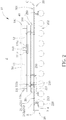
- FIG. 2 is a schematic, cross-sectional diagram taken alone line I-I' in FIG. 1 .
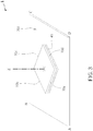
- FIG. 3 is a perspective view of the electronic package according to one embodiment of the invention.
- an electronic package 1 comprises a chip package 10 that is mounted on a top surface 201 of a package substrate 20 in a flip-chip manner.
- the chip package 10 and the package substrate 20 may both have a rectangular shape when viewed from the above.
- the chip package 10 and the package substrate 20 may both have a square shape having four sides of equal length.
- the chip package 10 has four sides 10a ⁇ 10d.
- the package substrate 20 has four vertices A ⁇ D and four sides 20a ⁇ 20d between the four vertices A ⁇ D, respectively.
- the top surface 201 of the package substrate 20 may be partitioned into four 90-degree quadrants Q 1 ⁇ Q 4 by two orthogonal axes (reference X and Y axes) in a two-dimensional plane (parallel to the top surface 201).
- the quadrants Q 1 and Q 3 are diagonally opposite each other.
- the quadrants Q 2 and Q 4 are diagonally opposite each other
- FIG. 1 to FIG. 3 a reference Z axis that is orthogonal to the top surface 201 or X-Y plane is shown.
- the package substrate 20 may be an organic substrate comprising laminated organic material or a core 200, such as epoxy or the like. As shown in FIG. 2 , a plurality of solder balls 230 may be disposed on a bottom surface 202 of the package substrate 20.
- the chip package 10 is mounted on the top surface 201 of a package substrate 20 through a plurality of solder joints or bumps 30.
- An underfill 40 may be dispensed to fill a gap (or standoff) between the chip package 10 and the package substrate 20.
- the package substrate 20 may comprise multiple layers of traces, for example, traces 211 and 221.
- the trace 211 is intended to be disposed in the topmost layer of the multiple layers of traces of the package substrate 20.
- the traces 211 may be covered with a protection layer 280 such as a solder mask or the like, but is not limited thereto.
- the bump 30 is joined to and aligned with a corresponding bump pad 210 at one distal end of the trace 211.
- the trace 211 extends toward the corner at the vertex A or toward the two adjacent sides 20a and 20b around the corner.
- the traces 211 for electrically connecting the corresponding bump pads 210 are generally disposed within the exemplary revealed quadrant Q 2 .
- the trace 211 is electrically coupled to a connection pad 212.
- a plated through hole (PTH) 213 may be provided to electrically connect the connection pad 212 to a solder ball pad 214 at the bottom surface 202 of the package substrate 20.
- a solder ball 230 is planted on the solder ball pad 214 for further connection with a system board or a printed circuit board (PCB).
- PCB printed circuit board
- connection pads 212 is aligned with the solder ball pads 214 and therefore the solder balls 230, the position of each connection pad 212 in FIG. 1 generally represents the position of each solder ball 230. It is understood that the configuration as indicated in quadrant Q 2 may be employed in the other quadrants Q 1 , Q 3 and Q 4 in other embodiments.
- the chip package 10 and the package substrate 20 may have the same center point CP and therefore have a concentric configuration with the chip package that is angular offset relative to the package substrate 20.
- the chip package 10 is rotated relative to the package substrate 20 above the Z axis through about 45 degrees.
- none of the four sides 10a ⁇ 10d of the chip package 10 is parallel with any of the four sides 20a ⁇ 20d of the package substrate 20.
- the chip package 10 It is intended to rotate the chip package 10 such that its one side 10a directly faces one corner at vertex A of the package substrate 20.
- the two sides 20a and 20b of the package substrate 20 are joined at the vertex A.
- the two sides 20a and 20b define boundaries of the 90-degree quadrant Q 2 .
- the chip package 10 comprises a first high-speed interface circuit die 11, which may be operated at high-speed data transmission rate of at least 1000Mbps at frequency higher than 500MHz.
- the first high-speed interface circuit die 11 may be encapsulated within a molding compound 50.
- the first high-speed interface circuit die 11 comprises a first Serializer/Deserializer (SerDes) circuit block 110 that is located in close proximity to the side 10a that directly faces one corner at vertex A of the package substrate 20.
- SerDes Serializer/Deserializer
- the first high-speed interface circuit die 11 comprises a first edge 11a directly facing the corner at the vertex A of the package substrate 20, a second edge 11b that is perpendicular to the first edge 11a and is joined to the first edge 11a, and a third edge 11c that is perpendicular to the first edge 11a and is joined to the first edge 11a.
- the first edge 11a is in parallel with the side 10a of the chip package 10
- the second edge 11b is in parallel with the side 10d of the chip package
- the third edge 11c is parallel with the side 10b of the chip package 10.
- the second edge 11b and the third edge 11c are in parallel with a diagonal line DL extending between the vertex A and the vertex C.
- a first row of input/output (I/O) pads 111a is disposed along the first edge 11a
- a second row of I/O pads 111b is disposed along the second edge 11b
- a third row of I/O pads 111c is disposed along the third edge 11c. It is understood that these I/O pads 111 are disposed at a bottom of the first high-speed interface circuit die 11.
- a redistribution layer (RDL) structure 100 may be provided between the first high-speed interface circuit die 11 and the top surface 201 of the package substrate 20 to fan-out the I/O pads 111.
- the RDL structure 100 which is known in the art, may be composed of dielectric layers and interconnect structures in the dielectric layers for electrically connecting the I/O pads of the high-speed interface circuit die 11 to the corresponding bump pads 101 wherein the solder joint 30 is formed.
- the chip package 10 may be a fan-out wafer level package (FOWLP).
- the first SerDes circuit block 110 of the first high-speed interface circuit die 11, the edges 11a ⁇ 11c, the rows of I/O pads 111a ⁇ 111c are generally disposed within the exemplary quadrant Q 2 . It is understood that the chip package 10 is flipped with its active surface mounted on the top surface 201 of the package substrate 20 in a flip-chip manner.
- a first group of solder balls P 1 solder balls are not explicitly shown in FIG. 1 , but aligned with the connection pads 212a
- the first row of I/O pads 111a disposed at the first edge 11a of the high-speed interface circuit die 11 is electrically connected to the first group of solder balls P 1 through the traces 211a, respectively, within the quadrant Q 2 on the top surface 201 of the package substrate 20.
- a second group of solder balls P 2 (solder balls are not explicitly shown in FIG. 1 , but aligned with the connection pads 212b) is arranged along the side 20a adjacent to the corner at the vertex A.
- the second row of I/O pads 111b is electrically connected to the second group of solder balls P 2 through traces 211b, respectively, within the quadrant Q 2 on the top surface 201 of the package substrate 20.
- a third group of solder balls P 3 (solder balls are not explicitly shown in FIG. 1 , but aligned with the connection pads 212c) is arranged along the side 20b adjacent to the corner at the vertex A.
- the second row of I/O pads 111c is electrically connected to the third group of solder balls P 3 through traces 211c, respectively, within the quadrant Q 2 on the top surface 201 of the package substrate 20.
- the chip package 10 may further comprises a second high-speed interface circuit die 12 in proximity to the first high-speed interface circuit die 11.
- the second high-speed interface circuit die 12 may comprise a SerDes circuit block 120 and may have similar trace and ball arrangement in the quadrant Q 4 of the top surface 201 of the package substrate 20.
- the first high-speed interface circuit die 11 may be electrically connected to the second high-speed interface circuit die 12 through the RDL structure 100.
- the I/O pad 111c of the first high-speed interface circuit die 11 is electrically connected to the I/O pad 121c of the second high-speed interface circuit die 12 through the interconnect line 103 in the RDL structure 100.
- the present disclosure because by providing the rotated chip package configuration, the corresponding traces and ball arrangement on the package substrate are concentrated within one of the four quadrants Q 1 ⁇ Q 4 , resulting in a 14.3% reduction of the maximum signal length (e.g., from about 35mm to about30mm for 60x60mm ⁇ 90x90mm package substrate), and a significant reduction of trace length difference (max. length minus min. length) from 20mm to 13mm. Therefore, the skew is mitigated and the signal delay as well as the electrical performance of SerDes circuit of the electronic package can be significantly improved (e.g., with improvement by 18% or about -0.5dB).
Landscapes
- Semiconductor Integrated Circuits (AREA)
- Wire Bonding (AREA)
Applications Claiming Priority (2)
| Application Number | Priority Date | Filing Date | Title |
|---|---|---|---|
| US201862673194P | 2018-05-18 | 2018-05-18 | |
| US16/398,228 US20190355697A1 (en) | 2018-05-18 | 2019-04-29 | Electronic package for high-data rate communication applications |
Publications (2)
| Publication Number | Publication Date |
|---|---|
| EP3582260A2 true EP3582260A2 (de) | 2019-12-18 |
| EP3582260A3 EP3582260A3 (de) | 2020-01-22 |
Family
ID=66542011
Family Applications (1)
| Application Number | Title | Priority Date | Filing Date |
|---|---|---|---|
| EP19172944.1A Withdrawn EP3582260A3 (de) | 2018-05-18 | 2019-05-07 | Elektronisches gehäuse für kommunikationsanwendungen mit hohen datenraten |
Country Status (4)
| Country | Link |
|---|---|
| US (1) | US20190355697A1 (de) |
| EP (1) | EP3582260A3 (de) |
| CN (1) | CN110504221A (de) |
| TW (1) | TW202005013A (de) |
Cited By (1)
| Publication number | Priority date | Publication date | Assignee | Title |
|---|---|---|---|---|
| EP3739626A1 (de) * | 2019-05-15 | 2020-11-18 | MediaTek Inc. | Elektronische packung mit rotiertem halbleiterchip |
Families Citing this family (2)
| Publication number | Priority date | Publication date | Assignee | Title |
|---|---|---|---|---|
| US11289398B2 (en) * | 2019-09-27 | 2022-03-29 | Taiwan Semiconductor Manufacturing Company, Ltd. | Package structure and manufacturing method thereof |
| US12002780B2 (en) * | 2020-11-12 | 2024-06-04 | Taiwan Semiconductor Manufacturing Company Ltd. | Package structure including a base and a lid disposed over the base and method of forming the package structure |
Family Cites Families (7)
| Publication number | Priority date | Publication date | Assignee | Title |
|---|---|---|---|---|
| US6118670A (en) * | 1998-06-30 | 2000-09-12 | Hewlett-Packard Company | PCB mounting arrangement for two components requiring high-speed connections to a third component |
| DE10202878A1 (de) * | 2002-01-25 | 2003-08-07 | Infineon Technologies Ag | Schaltungsplatine mit integrierter Schaltung zur Hochgeschwindigkeitsdatenverarbeitung |
| US7341887B2 (en) * | 2004-10-29 | 2008-03-11 | Intel Corporation | Integrated circuit die configuration for packaging |
| US8237289B2 (en) * | 2007-01-30 | 2012-08-07 | Kabushiki Kaisha Toshiba | System in package device |
| JP5313887B2 (ja) * | 2007-05-31 | 2013-10-09 | 三洋電機株式会社 | 半導体モジュールおよび携帯機器 |
| WO2011016157A1 (ja) * | 2009-08-07 | 2011-02-10 | パナソニック株式会社 | 半導体装置および電子装置 |
| WO2017029767A1 (ja) * | 2015-08-20 | 2017-02-23 | ルネサスエレクトロニクス株式会社 | 半導体装置 |
-
2019
- 2019-04-29 US US16/398,228 patent/US20190355697A1/en not_active Abandoned
- 2019-05-07 EP EP19172944.1A patent/EP3582260A3/de not_active Withdrawn
- 2019-05-10 CN CN201910387824.1A patent/CN110504221A/zh not_active Withdrawn
- 2019-05-16 TW TW108116862A patent/TW202005013A/zh unknown
Cited By (4)
| Publication number | Priority date | Publication date | Assignee | Title |
|---|---|---|---|---|
| EP3739626A1 (de) * | 2019-05-15 | 2020-11-18 | MediaTek Inc. | Elektronische packung mit rotiertem halbleiterchip |
| US11222850B2 (en) | 2019-05-15 | 2022-01-11 | Mediatek Inc. | Electronic package with rotated semiconductor die |
| US11830820B2 (en) | 2019-05-15 | 2023-11-28 | Mediatek Inc. | Electronic package with rotated semiconductor die |
| US12388026B2 (en) | 2019-05-15 | 2025-08-12 | Mediatek Inc. | Electronic package with rotated semiconductor die |
Also Published As
| Publication number | Publication date |
|---|---|
| EP3582260A3 (de) | 2020-01-22 |
| US20190355697A1 (en) | 2019-11-21 |
| TW202005013A (zh) | 2020-01-16 |
| CN110504221A (zh) | 2019-11-26 |
Similar Documents
| Publication | Publication Date | Title |
|---|---|---|
| US12388026B2 (en) | Electronic package with rotated semiconductor die | |
| US10716207B2 (en) | Printed circuit board and integrated circuit package | |
| JP6088893B2 (ja) | 半導体装置及び配線基板 | |
| US8823177B2 (en) | Semiconductor device and package wiring substrate with matrix pattern external terminals for transmitting a differential signal | |
| US9425149B1 (en) | Integrated circuit package routing with reduced crosstalk | |
| US11211315B2 (en) | Semiconductor package with terminal pattern for increased channel density | |
| EP3582260A2 (de) | Elektronisches gehäuse für kommunikationsanwendungen mit hohen datenraten | |
| WO2007089885A2 (en) | Passive impedance equalization of high speed serial links | |
| US10490506B2 (en) | Packaged chip and signal transmission method based on packaged chip | |
| WO2017111830A1 (en) | Rlink-ground shielding attachment structures and shadow voiding for data signal contacts of package devices; vertical ground shielding structures and shield fencing of vertical data signal interconnects of package devices; and ground shielding for electro optical module connector data signal contacts and contact pins of package devices | |
| JP7228532B2 (ja) | 低クロストークの垂直接続インターフェース | |
| CN104822225A (zh) | 一种电路板和印刷电路板组件 | |
| US6744130B1 (en) | Isolated stripline structure | |
| US20060043537A1 (en) | Routing differential signal lines in a substrate | |
| US9331370B1 (en) | Multilayer integrated circuit packages with localized air structures | |
| KR100805503B1 (ko) | 반도체 장치 및 그 제조 방법, 회로 기판, 및 전자기기 | |
| TW202117943A (zh) | 扇出型多晶片立體堆疊模組封裝架構 | |
| US7358607B2 (en) | Substrates and systems to minimize signal path discontinuities | |
| US20090032922A1 (en) | Semiconductor Package, Printed Wiring Board Structure and Electronic Apparatus | |
| US6639302B2 (en) | Stress reduction in flip-chip PBGA packaging by utilizing segmented chip carries | |
| KR102730708B1 (ko) | 스택 패키지 및 그의 제조 방법 | |
| WO2020024115A1 (zh) | 一种芯片组合件及终端设备 |
Legal Events
| Date | Code | Title | Description |
|---|---|---|---|
| PUAI | Public reference made under article 153(3) epc to a published international application that has entered the european phase |
Free format text: ORIGINAL CODE: 0009012 |
|
| AK | Designated contracting states |
Kind code of ref document: A2 Designated state(s): AL AT BE BG CH CY CZ DE DK EE ES FI FR GB GR HR HU IE IS IT LI LT LU LV MC MK MT NL NO PL PT RO RS SE SI SK SM TR |
|
| AX | Request for extension of the european patent |
Extension state: BA ME |
|
| PUAL | Search report despatched |
Free format text: ORIGINAL CODE: 0009013 |
|
| AK | Designated contracting states |
Kind code of ref document: A3 Designated state(s): AL AT BE BG CH CY CZ DE DK EE ES FI FR GB GR HR HU IE IS IT LI LT LU LV MC MK MT NL NO PL PT RO RS SE SI SK SM TR |
|
| AX | Request for extension of the european patent |
Extension state: BA ME |
|
| RIC1 | Information provided on ipc code assigned before grant |
Ipc: H01L 25/065 20060101ALN20191216BHEP Ipc: H01L 23/498 20060101AFI20191216BHEP Ipc: H05K 1/02 20060101ALI20191216BHEP Ipc: H01L 23/50 20060101ALI20191216BHEP |
|
| STAA | Information on the status of an ep patent application or granted ep patent |
Free format text: STATUS: THE APPLICATION IS DEEMED TO BE WITHDRAWN |
|
| 18D | Application deemed to be withdrawn |
Effective date: 20200723 |