EP3565011A1 - Lichtemittierende vorrichtung - Google Patents
Lichtemittierende vorrichtung Download PDFInfo
- Publication number
- EP3565011A1 EP3565011A1 EP19176082.6A EP19176082A EP3565011A1 EP 3565011 A1 EP3565011 A1 EP 3565011A1 EP 19176082 A EP19176082 A EP 19176082A EP 3565011 A1 EP3565011 A1 EP 3565011A1
- Authority
- EP
- European Patent Office
- Prior art keywords
- wavelength
- fluorescent material
- light emitting
- light
- emitting device
- Prior art date
- Legal status (The legal status is an assumption and is not a legal conclusion. Google has not performed a legal analysis and makes no representation as to the accuracy of the status listed.)
- Granted
Links
- 238000000295 emission spectrum Methods 0.000 claims abstract description 41
- 239000000463 material Substances 0.000 claims description 177
- 238000009877 rendering Methods 0.000 claims description 53
- 150000004767 nitrides Chemical class 0.000 claims description 28
- 150000004645 aluminates Chemical class 0.000 claims description 23
- 229920005989 resin Polymers 0.000 claims description 23
- 239000011347 resin Substances 0.000 claims description 23
- 229910019655 synthetic inorganic crystalline material Inorganic materials 0.000 claims description 20
- 229910052784 alkaline earth metal Inorganic materials 0.000 claims description 19
- 229910052782 aluminium Inorganic materials 0.000 claims description 17
- 229910052761 rare earth metal Inorganic materials 0.000 claims description 17
- 229910052688 Gadolinium Inorganic materials 0.000 claims description 16
- 229910052727 yttrium Inorganic materials 0.000 claims description 15
- 229910052693 Europium Inorganic materials 0.000 claims description 14
- 229910052788 barium Inorganic materials 0.000 claims description 14
- 229910052791 calcium Inorganic materials 0.000 claims description 14
- 229910052749 magnesium Inorganic materials 0.000 claims description 14
- 229910052712 strontium Inorganic materials 0.000 claims description 14
- 150000001342 alkaline earth metals Chemical class 0.000 claims description 13
- 229910052747 lanthanoid Inorganic materials 0.000 claims description 12
- 150000002602 lanthanoids Chemical class 0.000 claims description 12
- 229910052684 Cerium Inorganic materials 0.000 claims description 10
- 239000005084 Strontium aluminate Substances 0.000 claims description 10
- 229910052796 boron Inorganic materials 0.000 claims description 10
- 229910052733 gallium Inorganic materials 0.000 claims description 10
- 229910052725 zinc Inorganic materials 0.000 claims description 10
- 229910052771 Terbium Inorganic materials 0.000 claims description 9
- 229910052692 Dysprosium Inorganic materials 0.000 claims description 8
- 229910052779 Neodymium Inorganic materials 0.000 claims description 8
- 229910052691 Erbium Inorganic materials 0.000 claims description 7
- 229910052689 Holmium Inorganic materials 0.000 claims description 7
- 229910052777 Praseodymium Inorganic materials 0.000 claims description 7
- 229910052746 lanthanum Inorganic materials 0.000 claims description 7
- 229910052772 Samarium Inorganic materials 0.000 claims description 6
- 229910052736 halogen Inorganic materials 0.000 claims description 6
- 150000002367 halogens Chemical class 0.000 claims description 6
- 229910052751 metal Inorganic materials 0.000 claims description 6
- 239000002184 metal Substances 0.000 claims description 6
- 238000001228 spectrum Methods 0.000 claims description 6
- 229910052775 Thulium Inorganic materials 0.000 claims description 5
- 229910052748 manganese Inorganic materials 0.000 claims description 5
- 229910052757 nitrogen Inorganic materials 0.000 claims description 5
- 229910052706 scandium Inorganic materials 0.000 claims description 5
- 229910052710 silicon Inorganic materials 0.000 claims description 5
- BPQQTUXANYXVAA-UHFFFAOYSA-N Orthosilicate Chemical compound [O-][Si]([O-])([O-])[O-] BPQQTUXANYXVAA-UHFFFAOYSA-N 0.000 claims description 4
- 229910052769 Ytterbium Inorganic materials 0.000 claims description 4
- 229910052586 apatite Inorganic materials 0.000 claims description 4
- 229910052794 bromium Inorganic materials 0.000 claims description 4
- 229910052801 chlorine Inorganic materials 0.000 claims description 4
- 229910052731 fluorine Inorganic materials 0.000 claims description 4
- 229910052740 iodine Inorganic materials 0.000 claims description 4
- VSIIXMUUUJUKCM-UHFFFAOYSA-D pentacalcium;fluoride;triphosphate Chemical compound [F-].[Ca+2].[Ca+2].[Ca+2].[Ca+2].[Ca+2].[O-]P([O-])([O-])=O.[O-]P([O-])([O-])=O.[O-]P([O-])([O-])=O VSIIXMUUUJUKCM-UHFFFAOYSA-D 0.000 claims description 4
- UCKMPCXJQFINFW-UHFFFAOYSA-N Sulphide Chemical compound [S-2] UCKMPCXJQFINFW-UHFFFAOYSA-N 0.000 claims description 3
- 229910052723 transition metal Inorganic materials 0.000 claims description 3
- 229910052581 Si3N4 Inorganic materials 0.000 claims description 2
- 229910003669 SrAl2O4 Inorganic materials 0.000 claims description 2
- 229910001650 dmitryivanovite Inorganic materials 0.000 claims description 2
- 239000002223 garnet Substances 0.000 claims description 2
- 229910001707 krotite Inorganic materials 0.000 claims description 2
- 150000002894 organic compounds Chemical class 0.000 claims description 2
- HQVNEWCFYHHQES-UHFFFAOYSA-N silicon nitride Chemical compound N12[Si]34N5[Si]62N3[Si]51N64 HQVNEWCFYHHQES-UHFFFAOYSA-N 0.000 claims description 2
- 229910019901 yttrium aluminum garnet Inorganic materials 0.000 claims description 2
- OAICVXFJPJFONN-UHFFFAOYSA-N Phosphorus Chemical compound [P] OAICVXFJPJFONN-UHFFFAOYSA-N 0.000 claims 1
- 230000000052 comparative effect Effects 0.000 description 30
- 239000000203 mixture Substances 0.000 description 26
- 239000004065 semiconductor Substances 0.000 description 14
- 239000011575 calcium Substances 0.000 description 12
- 239000011777 magnesium Substances 0.000 description 12
- 239000011701 zinc Substances 0.000 description 10
- 230000001681 protective effect Effects 0.000 description 9
- 238000002156 mixing Methods 0.000 description 8
- 239000003990 capacitor Substances 0.000 description 7
- 229910052765 Lutetium Inorganic materials 0.000 description 6
- 230000004907 flux Effects 0.000 description 5
- 230000001965 increasing effect Effects 0.000 description 5
- 238000000034 method Methods 0.000 description 5
- ZOXJGFHDIHLPTG-UHFFFAOYSA-N Boron Chemical compound [B] ZOXJGFHDIHLPTG-UHFFFAOYSA-N 0.000 description 4
- VTYYLEPIZMXCLO-UHFFFAOYSA-L Calcium carbonate Chemical compound [Ca+2].[O-]C([O-])=O VTYYLEPIZMXCLO-UHFFFAOYSA-L 0.000 description 4
- 230000015556 catabolic process Effects 0.000 description 4
- 239000003086 colorant Substances 0.000 description 4
- 150000001875 compounds Chemical class 0.000 description 4
- 230000002596 correlated effect Effects 0.000 description 4
- 238000006731 degradation reaction Methods 0.000 description 4
- 239000011521 glass Substances 0.000 description 4
- 229910052726 zirconium Inorganic materials 0.000 description 4
- PXHVJJICTQNCMI-UHFFFAOYSA-N Nickel Chemical compound [Ni] PXHVJJICTQNCMI-UHFFFAOYSA-N 0.000 description 3
- VYPSYNLAJGMNEJ-UHFFFAOYSA-N Silicium dioxide Chemical compound O=[Si]=O VYPSYNLAJGMNEJ-UHFFFAOYSA-N 0.000 description 3
- PNEYBMLMFCGWSK-UHFFFAOYSA-N aluminium oxide Inorganic materials [O-2].[O-2].[O-2].[Al+3].[Al+3] PNEYBMLMFCGWSK-UHFFFAOYSA-N 0.000 description 3
- 239000000919 ceramic Substances 0.000 description 3
- 229910052732 germanium Inorganic materials 0.000 description 3
- 229910052737 gold Inorganic materials 0.000 description 3
- 239000010931 gold Substances 0.000 description 3
- 239000004973 liquid crystal related substance Substances 0.000 description 3
- 229910052719 titanium Inorganic materials 0.000 description 3
- 239000010936 titanium Substances 0.000 description 3
- IJGRMHOSHXDMSA-UHFFFAOYSA-N Atomic nitrogen Chemical compound N#N IJGRMHOSHXDMSA-UHFFFAOYSA-N 0.000 description 2
- XEEYBQQBJWHFJM-UHFFFAOYSA-N Iron Chemical compound [Fe] XEEYBQQBJWHFJM-UHFFFAOYSA-N 0.000 description 2
- 229920000106 Liquid crystal polymer Polymers 0.000 description 2
- 239000004977 Liquid-crystal polymers (LCPs) Substances 0.000 description 2
- 239000004734 Polyphenylene sulfide Substances 0.000 description 2
- XLOMVQKBTHCTTD-UHFFFAOYSA-N Zinc monoxide Chemical compound [Zn]=O XLOMVQKBTHCTTD-UHFFFAOYSA-N 0.000 description 2
- 239000000654 additive Substances 0.000 description 2
- -1 alkaline earth metal sulfide Chemical class 0.000 description 2
- 229910052790 beryllium Inorganic materials 0.000 description 2
- 229910000019 calcium carbonate Inorganic materials 0.000 description 2
- 229910052799 carbon Inorganic materials 0.000 description 2
- 238000006243 chemical reaction Methods 0.000 description 2
- 239000003795 chemical substances by application Substances 0.000 description 2
- 229910052593 corundum Inorganic materials 0.000 description 2
- 230000006378 damage Effects 0.000 description 2
- 239000003822 epoxy resin Substances 0.000 description 2
- PCHJSUWPFVWCPO-UHFFFAOYSA-N gold Chemical compound [Au] PCHJSUWPFVWCPO-UHFFFAOYSA-N 0.000 description 2
- 229910021480 group 4 element Inorganic materials 0.000 description 2
- 229910052735 hafnium Inorganic materials 0.000 description 2
- 150000002500 ions Chemical class 0.000 description 2
- 238000004519 manufacturing process Methods 0.000 description 2
- 238000005259 measurement Methods 0.000 description 2
- 229910052759 nickel Inorganic materials 0.000 description 2
- 229920000647 polyepoxide Polymers 0.000 description 2
- 229920000642 polymer Polymers 0.000 description 2
- 229920000069 polyphenylene sulfide Polymers 0.000 description 2
- 229910001404 rare earth metal oxide Inorganic materials 0.000 description 2
- 229910052594 sapphire Inorganic materials 0.000 description 2
- 239000010980 sapphire Substances 0.000 description 2
- 229920002050 silicone resin Polymers 0.000 description 2
- 229910052709 silver Inorganic materials 0.000 description 2
- 230000003595 spectral effect Effects 0.000 description 2
- 239000000758 substrate Substances 0.000 description 2
- 229920001169 thermoplastic Polymers 0.000 description 2
- 239000004416 thermosoftening plastic Substances 0.000 description 2
- 229910052718 tin Inorganic materials 0.000 description 2
- 229910001845 yogo sapphire Inorganic materials 0.000 description 2
- 229910002704 AlGaN Inorganic materials 0.000 description 1
- 229910052582 BN Inorganic materials 0.000 description 1
- PZNSFCLAULLKQX-UHFFFAOYSA-N Boron nitride Chemical compound N#B PZNSFCLAULLKQX-UHFFFAOYSA-N 0.000 description 1
- RYGMFSIKBFXOCR-UHFFFAOYSA-N Copper Chemical compound [Cu] RYGMFSIKBFXOCR-UHFFFAOYSA-N 0.000 description 1
- 229910000881 Cu alloy Inorganic materials 0.000 description 1
- 229910000640 Fe alloy Inorganic materials 0.000 description 1
- 229910005833 GeO4 Inorganic materials 0.000 description 1
- 229910002226 La2O2 Inorganic materials 0.000 description 1
- 229910015811 MSi2 Inorganic materials 0.000 description 1
- 229910019142 PO4 Inorganic materials 0.000 description 1
- BQCADISMDOOEFD-UHFFFAOYSA-N Silver Chemical compound [Ag] BQCADISMDOOEFD-UHFFFAOYSA-N 0.000 description 1
- 229910006360 Si—O—N Inorganic materials 0.000 description 1
- GWEVSGVZZGPLCZ-UHFFFAOYSA-N Titan oxide Chemical compound O=[Ti]=O GWEVSGVZZGPLCZ-UHFFFAOYSA-N 0.000 description 1
- 239000006096 absorbing agent Substances 0.000 description 1
- XAGFODPZIPBFFR-UHFFFAOYSA-N aluminium Chemical compound [Al] XAGFODPZIPBFFR-UHFFFAOYSA-N 0.000 description 1
- 229920006020 amorphous polyamide Polymers 0.000 description 1
- 229920003233 aromatic nylon Polymers 0.000 description 1
- JRPBQTZRNDNNOP-UHFFFAOYSA-N barium titanate Chemical compound [Ba+2].[Ba+2].[O-][Ti]([O-])([O-])[O-] JRPBQTZRNDNNOP-UHFFFAOYSA-N 0.000 description 1
- 229910002113 barium titanate Inorganic materials 0.000 description 1
- 239000001506 calcium phosphate Substances 0.000 description 1
- 229910000389 calcium phosphate Inorganic materials 0.000 description 1
- 235000011010 calcium phosphates Nutrition 0.000 description 1
- 230000008859 change Effects 0.000 description 1
- 229910052804 chromium Inorganic materials 0.000 description 1
- 239000011651 chromium Substances 0.000 description 1
- 230000006690 co-activation Effects 0.000 description 1
- 239000004020 conductor Substances 0.000 description 1
- 238000010276 construction Methods 0.000 description 1
- 230000001276 controlling effect Effects 0.000 description 1
- 229910052802 copper Inorganic materials 0.000 description 1
- 239000010949 copper Substances 0.000 description 1
- 239000011889 copper foil Substances 0.000 description 1
- 230000003247 decreasing effect Effects 0.000 description 1
- 239000002270 dispersing agent Substances 0.000 description 1
- 239000006185 dispersion Substances 0.000 description 1
- 230000000694 effects Effects 0.000 description 1
- 238000007772 electroless plating Methods 0.000 description 1
- 238000009713 electroplating Methods 0.000 description 1
- 230000002708 enhancing effect Effects 0.000 description 1
- 238000003912 environmental pollution Methods 0.000 description 1
- 238000005530 etching Methods 0.000 description 1
- 239000000945 filler Substances 0.000 description 1
- 239000007850 fluorescent dye Substances 0.000 description 1
- NBVXSUQYWXRMNV-UHFFFAOYSA-N fluoromethane Chemical compound FC NBVXSUQYWXRMNV-UHFFFAOYSA-N 0.000 description 1
- 239000003365 glass fiber Substances 0.000 description 1
- 229910052738 indium Inorganic materials 0.000 description 1
- 239000011256 inorganic filler Substances 0.000 description 1
- 229910003475 inorganic filler Inorganic materials 0.000 description 1
- 239000004611 light stabiliser Substances 0.000 description 1
- ZLNQQNXFFQJAID-UHFFFAOYSA-L magnesium carbonate Chemical compound [Mg+2].[O-]C([O-])=O ZLNQQNXFFQJAID-UHFFFAOYSA-L 0.000 description 1
- 239000001095 magnesium carbonate Substances 0.000 description 1
- 229910000021 magnesium carbonate Inorganic materials 0.000 description 1
- QSHDDOUJBYECFT-UHFFFAOYSA-N mercury Chemical compound [Hg] QSHDDOUJBYECFT-UHFFFAOYSA-N 0.000 description 1
- 229910052753 mercury Inorganic materials 0.000 description 1
- 230000004048 modification Effects 0.000 description 1
- 238000012986 modification Methods 0.000 description 1
- 238000007254 oxidation reaction Methods 0.000 description 1
- 239000000049 pigment Substances 0.000 description 1
- 230000003449 preventive effect Effects 0.000 description 1
- 230000008569 process Effects 0.000 description 1
- 230000009467 reduction Effects 0.000 description 1
- 230000003252 repetitive effect Effects 0.000 description 1
- 238000011160 research Methods 0.000 description 1
- 230000002441 reversible effect Effects 0.000 description 1
- 239000000377 silicon dioxide Substances 0.000 description 1
- 239000004332 silver Substances 0.000 description 1
- 239000010944 silver (metal) Substances 0.000 description 1
- 239000000454 talc Substances 0.000 description 1
- 229910052623 talc Inorganic materials 0.000 description 1
- 239000003017 thermal stabilizer Substances 0.000 description 1
- 229920001187 thermosetting polymer Polymers 0.000 description 1
- OGIDPMRJRNCKJF-UHFFFAOYSA-N titanium oxide Inorganic materials [Ti]=O OGIDPMRJRNCKJF-UHFFFAOYSA-N 0.000 description 1
- 229910000314 transition metal oxide Inorganic materials 0.000 description 1
- QORWJWZARLRLPR-UHFFFAOYSA-H tricalcium bis(phosphate) Chemical compound [Ca+2].[Ca+2].[Ca+2].[O-]P([O-])([O-])=O.[O-]P([O-])([O-])=O QORWJWZARLRLPR-UHFFFAOYSA-H 0.000 description 1
- 230000000007 visual effect Effects 0.000 description 1
- 239000011787 zinc oxide Substances 0.000 description 1
Images


Classifications
-
- C—CHEMISTRY; METALLURGY
- C09—DYES; PAINTS; POLISHES; NATURAL RESINS; ADHESIVES; COMPOSITIONS NOT OTHERWISE PROVIDED FOR; APPLICATIONS OF MATERIALS NOT OTHERWISE PROVIDED FOR
- C09K—MATERIALS FOR MISCELLANEOUS APPLICATIONS, NOT PROVIDED FOR ELSEWHERE
- C09K11/00—Luminescent, e.g. electroluminescent, chemiluminescent materials
- C09K11/08—Luminescent, e.g. electroluminescent, chemiluminescent materials containing inorganic luminescent materials
- C09K11/77—Luminescent, e.g. electroluminescent, chemiluminescent materials containing inorganic luminescent materials containing rare earth metals
- C09K11/7766—Luminescent, e.g. electroluminescent, chemiluminescent materials containing inorganic luminescent materials containing rare earth metals containing two or more rare earth metals
- C09K11/7774—Aluminates
-
- C—CHEMISTRY; METALLURGY
- C09—DYES; PAINTS; POLISHES; NATURAL RESINS; ADHESIVES; COMPOSITIONS NOT OTHERWISE PROVIDED FOR; APPLICATIONS OF MATERIALS NOT OTHERWISE PROVIDED FOR
- C09K—MATERIALS FOR MISCELLANEOUS APPLICATIONS, NOT PROVIDED FOR ELSEWHERE
- C09K11/00—Luminescent, e.g. electroluminescent, chemiluminescent materials
- C09K11/08—Luminescent, e.g. electroluminescent, chemiluminescent materials containing inorganic luminescent materials
- C09K11/66—Luminescent, e.g. electroluminescent, chemiluminescent materials containing inorganic luminescent materials containing germanium, tin or lead
- C09K11/661—Chalcogenides
- C09K11/662—Chalcogenides with zinc or cadmium
-
- C—CHEMISTRY; METALLURGY
- C09—DYES; PAINTS; POLISHES; NATURAL RESINS; ADHESIVES; COMPOSITIONS NOT OTHERWISE PROVIDED FOR; APPLICATIONS OF MATERIALS NOT OTHERWISE PROVIDED FOR
- C09K—MATERIALS FOR MISCELLANEOUS APPLICATIONS, NOT PROVIDED FOR ELSEWHERE
- C09K11/00—Luminescent, e.g. electroluminescent, chemiluminescent materials
- C09K11/08—Luminescent, e.g. electroluminescent, chemiluminescent materials containing inorganic luminescent materials
- C09K11/77—Luminescent, e.g. electroluminescent, chemiluminescent materials containing inorganic luminescent materials containing rare earth metals
- C09K11/7766—Luminescent, e.g. electroluminescent, chemiluminescent materials containing inorganic luminescent materials containing rare earth metals containing two or more rare earth metals
- C09K11/7767—Chalcogenides
- C09K11/7769—Oxides
- C09K11/7771—Oxysulfides
-
- C—CHEMISTRY; METALLURGY
- C09—DYES; PAINTS; POLISHES; NATURAL RESINS; ADHESIVES; COMPOSITIONS NOT OTHERWISE PROVIDED FOR; APPLICATIONS OF MATERIALS NOT OTHERWISE PROVIDED FOR
- C09K—MATERIALS FOR MISCELLANEOUS APPLICATIONS, NOT PROVIDED FOR ELSEWHERE
- C09K11/00—Luminescent, e.g. electroluminescent, chemiluminescent materials
- C09K11/08—Luminescent, e.g. electroluminescent, chemiluminescent materials containing inorganic luminescent materials
- C09K11/77—Luminescent, e.g. electroluminescent, chemiluminescent materials containing inorganic luminescent materials containing rare earth metals
- C09K11/7783—Luminescent, e.g. electroluminescent, chemiluminescent materials containing inorganic luminescent materials containing rare earth metals containing two or more rare earth metals one of which being europium
- C09K11/7784—Chalcogenides
- C09K11/7785—Chalcogenides with zinc or cadmium
-
- H—ELECTRICITY
- H01—ELECTRIC ELEMENTS
- H01L—SEMICONDUCTOR DEVICES NOT COVERED BY CLASS H10
- H01L33/00—Semiconductor devices with at least one potential-jump barrier or surface barrier specially adapted for light emission; Processes or apparatus specially adapted for the manufacture or treatment thereof or of parts thereof; Details thereof
- H01L33/48—Semiconductor devices with at least one potential-jump barrier or surface barrier specially adapted for light emission; Processes or apparatus specially adapted for the manufacture or treatment thereof or of parts thereof; Details thereof characterised by the semiconductor body packages
- H01L33/50—Wavelength conversion elements
-
- H—ELECTRICITY
- H01—ELECTRIC ELEMENTS
- H01L—SEMICONDUCTOR DEVICES NOT COVERED BY CLASS H10
- H01L2224/00—Indexing scheme for arrangements for connecting or disconnecting semiconductor or solid-state bodies and methods related thereto as covered by H01L24/00
- H01L2224/01—Means for bonding being attached to, or being formed on, the surface to be connected, e.g. chip-to-package, die-attach, "first-level" interconnects; Manufacturing methods related thereto
- H01L2224/42—Wire connectors; Manufacturing methods related thereto
- H01L2224/47—Structure, shape, material or disposition of the wire connectors after the connecting process
- H01L2224/48—Structure, shape, material or disposition of the wire connectors after the connecting process of an individual wire connector
- H01L2224/4805—Shape
- H01L2224/4809—Loop shape
- H01L2224/48091—Arched
-
- H—ELECTRICITY
- H01—ELECTRIC ELEMENTS
- H01L—SEMICONDUCTOR DEVICES NOT COVERED BY CLASS H10
- H01L2224/00—Indexing scheme for arrangements for connecting or disconnecting semiconductor or solid-state bodies and methods related thereto as covered by H01L24/00
- H01L2224/01—Means for bonding being attached to, or being formed on, the surface to be connected, e.g. chip-to-package, die-attach, "first-level" interconnects; Manufacturing methods related thereto
- H01L2224/42—Wire connectors; Manufacturing methods related thereto
- H01L2224/47—Structure, shape, material or disposition of the wire connectors after the connecting process
- H01L2224/48—Structure, shape, material or disposition of the wire connectors after the connecting process of an individual wire connector
- H01L2224/481—Disposition
- H01L2224/48151—Connecting between a semiconductor or solid-state body and an item not being a semiconductor or solid-state body, e.g. chip-to-substrate, chip-to-passive
- H01L2224/48221—Connecting between a semiconductor or solid-state body and an item not being a semiconductor or solid-state body, e.g. chip-to-substrate, chip-to-passive the body and the item being stacked
- H01L2224/48245—Connecting between a semiconductor or solid-state body and an item not being a semiconductor or solid-state body, e.g. chip-to-substrate, chip-to-passive the body and the item being stacked the item being metallic
- H01L2224/48247—Connecting between a semiconductor or solid-state body and an item not being a semiconductor or solid-state body, e.g. chip-to-substrate, chip-to-passive the body and the item being stacked the item being metallic connecting the wire to a bond pad of the item
-
- H—ELECTRICITY
- H01—ELECTRIC ELEMENTS
- H01L—SEMICONDUCTOR DEVICES NOT COVERED BY CLASS H10
- H01L33/00—Semiconductor devices with at least one potential-jump barrier or surface barrier specially adapted for light emission; Processes or apparatus specially adapted for the manufacture or treatment thereof or of parts thereof; Details thereof
- H01L33/48—Semiconductor devices with at least one potential-jump barrier or surface barrier specially adapted for light emission; Processes or apparatus specially adapted for the manufacture or treatment thereof or of parts thereof; Details thereof characterised by the semiconductor body packages
- H01L33/50—Wavelength conversion elements
- H01L33/501—Wavelength conversion elements characterised by the materials, e.g. binder
- H01L33/502—Wavelength conversion materials
- H01L33/504—Elements with two or more wavelength conversion materials
Definitions
- the present invention relates to a light emitting device used in a liquid crystal backlight light source, lighting apparatus, backlight light source for display, flash of a camera, auxiliary light source for movies, etc., and particularly to a light emitting device requiring color rendering performance.
- the fluorescent lamp is used as a popular lighting apparatus.
- growing concern for environmental pollution increases the demand for light sources which are free of mercury, and light emitting devices based on light emitting elements such as light emitting diodes (hereinafter referred to as LEDs) or laser diodes (hereinafter referred to as LDs) are attracting much attention.
- LEDs light emitting diodes
- LDs laser diodes
- Light emitting devices based on the light emitting elements are small in size, high in power efficiency and are capable of emitting light of vivid colors. Furthermore, such light emitting elements are semiconductor devices free of failure such as burnout. These light emitting elements also have such advantages as excellent startup characteristics and high tolerance to vibration and to repetitive turning ON/OFF. Because of such excellent characteristics, light emitting devices based on light emitting elements such as LEDs and LDs are used widely in various light sources.
- the first type is a light emitting device that combines a blue LED and a YAG fluorescent material which emits yellow light.
- the light emitting device emits white light by blending blue light and yellow light, whereas the YAG fluorescent material is excited by the blue light emitted by the blue LED.
- the light emitting device has the advantages of reduction in power consumption, easy control of the LED operation and good color blending performance, and therefore has been widely used.
- the second type is a light emitting device that combines a blue LED, a green LED and a red LED.
- This light emitting device is the so-called three-wavelength light emitting device that generates white light by blending the light from the three LEDs.
- the light emitting device is capable of reducing the power consumption, and has a wide range of display colors for light that passes through the liquid crystal.
- Patent Document 1 Japanese Unexamined Patent Publication (Kokai) No. 2003-45206
- the first light emitting device combines blue light and yellow light, and therefore has lower radiant flux in the blue-green region and in the red region than that of an incandescent lamp, thus resulting in uneven distribution of radiant flux intensity in the visible light region.
- the second light emitting device has difficulty in blending colors and poor color rendering performance. Since light emitted by an LED is sharp unlike the light emitted by a fluorescent lamp, it is difficult to achieve a continuous emission spectrum by blending the light from different LEDs. The energy intensity is particularly low in regions between the emission peaks of the LEDs. Also because three or more LEDs are required to make one light source, it becomes complicated to control the operation thereof and it is also difficult to adjust the color tone.
- an object When illuminated with the light emitted by such a light emitting device, an object may appear to have a surface color different from that when illuminated by a continuous-spectrum white light such as light from the sun or an incandescent lamp.
- a light emitting device that employs an ultraviolet LED instead of a blue LED is also known.
- a light emitting device that employs an ultraviolet LED and a fluorescent material is capable of reducing the unevenness in radiant flux intensity distribution in the visible light region.
- measures must be taken to prevent the ultraviolet rays from escaping to the outside.
- the ultraviolet rays also accelerate the degradation of the components.
- ultraviolet LED is practically undetectable by the naked eye, ultraviolet rays escaping from the light emitting device are useless as visual light, thus resulting in lower luminous efficiency.
- the present invention purposes to provide a light emitting device that is capable of reducing the unevenness in radiant flux intensity distribution in the visible light region and has a continuous spectrum similar to that of light from the sun or an incandescent lamp.
- the light emitting device of the present invention comprises a exciting light source that emits light of short wavelength in the visible light region and a wavelength converting member that absorbs light from the exciting light source and emits light of a wavelength longer than that of the light from the exciting light source, such that the light emitting device emits light with a color temperature in a range from 4, 000K to 5, 000K, wherein the light emitting device has a visible light emission spectrum with a wavelength at which the light from the exciting light source has a maximum energy intensity denoted as a first wavelength, a wavelength at which the light from the wavelength converting member has a maximum energy intensity denoted as a second wavelength, a wavelength lying between the first and second wavelengths at which the light from the light emitting device has a minimum energy intensity denoted as a third wavelength, and 650 nm denoted as a fourth wavelength, such that the proportion of the energy intensity at the first wavelength to the energy intensity at the third wavelength is from 100:15 to 100:150, and the proportion of the energy intensity at the first wavelength to
- a light emitting device having a continuous spectrum similar to that of light from the sun or an incandescent lamp is provided. It is also possible to increase the intensity of emission in the red region and improve the color rendering performance. Moreover, because the light emitting device employs an exciting light source that emits visible light, ultraviolet rays are hardly emitted so that degradation of components is avoided and there is no need to take preventive measures for leakage of ultraviolet rays.
- the wavelength converting member absorbs light from the exciting light source, an increase in the proportion of light absorbed by the wavelength converting member leads to a smaller proportion of light emitted by the exciting light source that emerges to the outside, thus making it difficult to produce light of the predetermined color temperature and color tone. For this reason, the exciting light source and the wavelength converting member are selected so that the energy intensity at the first wavelength and the energy intensities at the second through fourth wavelengths fall in the predetermined range.
- the light emitting device has a general color rendering index in a range from 75 to 99, which enables a light emitting device with higher color rendering performance.
- the exciting light source is a light emitting element
- the wavelength converting member comprises one fluorescent material or two or more kinds of fluorescent material having different compositions. Such a constitution enables a light emitting device of smaller size and high power efficiency.
- This constitution further increases the intensity of emission in the red region thereby to provide a continuous emission spectrum like that of light from the sun or an incandescent lamp.
- the wavelength converting member preferably comprises a nitride fluorescent material that includes at least one kind of group II element selected from the group consisting of Be, Mg, Ca, Sr, Ba and Zn; at least one kind of group IV element selected from the group consisting of C, Si, Ge, Sn, Ti, Zr and Hf; and at least one kind of group III element selected from the group consisting of Al, B and N with N included as an indispensable element, and is activated with at least one kind of rare earth element selected from the group consisting of Y, La, Ce, Pr, Nd, Sm, Eu, Gd, Tb, Dy, Ho, Er and Lu.
- group II element selected from the group consisting of Be, Mg, Ca, Sr, Ba and Zn
- group IV element selected from the group consisting of C, Si, Ge, Sn, Ti, Zr and Hf
- group III element selected from the group consisting of Al, B and N with N included as an indispensable element
- the nitride fluorescent material of such a composition has an emission peak at a longer wavelength in the visible light region, and therefore has higher energy intensity in the red region.
- the nitride fluorescent material also has a broad emission spectrum and therefore enables a light emitting device of high color rendering performance.
- the nitride fluorescent material has higher heat resistance than a fluorescent material based on sulfide or the like, and is less susceptible to thermal degradation.
- the present invention is capable of providing a light emitting device having mitigated unevenness in radiant flux intensity distribution in the visible light region, and also providing a light emitting device having high luminance with a continuous emission spectrum similar to that of light from the sun or an incandescent lamp.
- the present invention is also capable of providing a light emitting device having high color rendering performance with an improved color rendering index which is one indicator of the quality of illuminating light.
- the light emitting device and a method for manufacturing the same according to the present invention will now be described by way of embodiment and Examples. It is understood, however, that the present invention is not limited to the embodiment and Examples.
- Fig. 1 is a schematic perspective view showing the light emitting device according to an embodiment of the present invention.
- the wavelength converting member 50 is omitted for the sake of clearness.
- Fig. 2 is a sectional view showing a light emitting device according to the embodiment taken along lines II-II.
- the light emitting device 100 comprises a light emitting element 10 serving as an exciting light source, a package 20 having a recess constituted from a bottom surface 20a on which a light emitting element 10 is mounted thereon and a side face 20b extending from the bottom surface 20a, and a wavelength converting member 50.
- a first electrode 30a and a second electrode 30b are installed on a portion of the bottom surface 20a in the recess of the package 20.
- the first electrode 30a is connected to a corner and back face on the outside of the package 20, while said outside corner and the back face are electrically connected to an external electrode.
- the second electrode 30b is connected to the corner and the back face on the outside of the package 20, while the outside corner and the back face are electrically connected to an external electrode.
- the light emitting element 10 is mounted on the first electrode 30a that is provided on the bottom surface in the recess of the package 20.
- a fluorescent material 52 mixed in a resin 51 is used for the wavelength converting member 50.
- the light emitting element 10 is formed from, for example, a compound semiconductor based on GaN, in such a constitution as an n-type compound semiconductor layer formed on an insulating sapphire substrate, and a p-type compound semiconductor layer formed thereon. While the light emitting element 10 is mounted on the first electrode 30a with the sapphire substrate facing down, the light emitting element 10 may also be mounted on the first electrode 30a with the compound semiconductor side facing down.
- An n-side electrode formed on the n-type layer is electrically connected by a wire 40 to the first electrode 30a.
- a p-side electrode formed on the p-type layer is electrically connected by a wire 40 to the second electrode 30b.
- the first electrode 30a and the second electrode 30b are a pair of positive and negative electrodes.
- the light emitting element 10 may be formed from a semiconductor based on InGaN, AlGaN, InAlGaN or the like as well as GaN.
- the light emitting element 10 is formed of a semiconductor that emits light of a short wavelength in the visible light region such as bluish purple light, blue light or green light. It is preferable that the light emitting element 10 has a peak emission wavelength in a range from 400 nm to 495 nm, more preferably in a range from 440 nm to 495 nm, because said wavelength range enables effective use of the transmitted light unable to be absorbed by the fluorescent material 52, ultraviolet rays are not emitted to the outside and the energy level is high.
- the package 20 has a recess that opens upward.
- the recess has a bottom surface 20a where the light emitting element 10 is mounted and a side face 20b extending from the bottom surface 20a.
- the bottom of the package 20 may have various shapes such as circular, elliptical, rectangular, polygonal or a modification thereof.
- the size of the package 20 which may be, for example, from 0.1 mm 2 to 100 mm 2 . Thickness of the package 20 may be in a range from 100 ⁇ m to 20 mm.
- the package 20 is made of ceramics, although the present invention is not limited to this constitution and known materials such as heat-resistant thermoplastic engineering polymers or thermosetting resins may be used individually or in a combination of two kinds or more thereof.
- thermoplastic engineering polymers such as thermoplastic polymers or thermosetting resins
- thermosetting resins such as thermoplastic polymers or thermosetting resins
- LCP liquid crystal polymer
- PPS polyphenylene sulfide
- PPA aromatic nylon
- epoxy resin hard silicone resin or the like
- a thermoplastic engineering polymer is preferably used due to cost advantages.
- the package 20 may also include additives including but not limited to one or a combination of two or more kinds of inorganic fillers such as titanium oxide, zinc oxide, alumina, silica, barium titanate, calcium phosphate, calcium carbonate, white carbon, talc, magnesium carbonate, boron nitride, glass fibers or the like. Moreover, additives such as anti-oxidization agents, thermal stabilizers, light stabilizers or the like may be added as required. While the recess of the package 20 has a circular opening, the opening may be formed in an elliptical, rectangular, polygonal or a modified shape thereof.
- the first electrode 30a and the second electrode 30b are molded integrally with the ceramic package 20.
- the first electrode 30a and the second electrode 30b may be finished by electroless plating, or may be a copper foil patterned and formed by such processes as exposure, etching and removal of resist mask, followed by electroplating with nickel and gold.
- the first electrode 30a and the second electrode 30b can be formed alternatively from a good heat conductor such as an alloy of copper or iron, which may be plated with silver, aluminum, gold or the like on the surface thereof.
- the light emitting element 10 is mounted via a bonding member directly on the first electrode 30a.
- the protective element 11 is also mounted on the first electrode 30a.
- the light emitting element 10 may also be mounted on the protective element 11 that is mounted on the first electrode 30a via a bonding member.
- the protective element 11 is an element that is housed together with semiconductor elements such as the light emitting element 10 in the recess of the package 20, and protects the other semiconductor elements from destruction by an over voltage.
- the protective element 11 may or may not have a semiconductor structure.
- a zener diode, capacitor, diac or the like may be used for example, a zener diode, capacitor, diac or the like may be used.
- a zener diode comprises a p-type semiconductor region having a positive electrode and an n-type semiconductor region having a negative electrode, with the negative electrode and the positive electrode of the protective element being connected to the p-side electrode and the n-side electrode of the light emitting element, respectively, in reverse parallel connection.
- a surface-mounted chip may be used.
- a capacitor of such a construction has band-shaped electrodes provided on either side, and these electrodes are connected to the positive and negative electrodes of the light emitting element in parallel connection.
- the over voltage causes a charging current to flow into the capacitor, thus instantaneously decreasing the voltage across the capacitor, so that the voltage applied across the light emitting element does not increase, thereby protecting the light emitting element from the over voltage.
- the capacitor when the element receives noise having a high frequency component, the capacitor functions as a bypass capacitor so as to shut out the extraneous noise.
- the wavelength converting member 50 comprising the fluorescent material 52 mixed in the resin 51.
- the resin 51 may further include a filler, dispersant, pigment, light absorbing agent or the like mixed therein.
- a fluorescent dye may be used instead of the fluorescent material 52 or together with the fluorescent material 52.
- the fluorescent material 52 absorbs light from the light emitting element 10 and emits light of a wavelength longer than that of the light from the light emitting element. This constitution has a high efficiency of energy conversion. While the resin 51 itself does not cause a significant change in wavelength, said resin allows the easy fixation of the fluorescent material 52 which is capable of wavelength conversion.
- the wavelength converting member 50 is thus formed by combining the fluorescent material 52 and the resin 51.
- the resin 51 may be highly heat-resistant silicone resin or epoxy resin, amorphous polyamide resin, fluorocarbon resin or the like. It is preferable to use a rare earth element aluminate fluorescent material activated by rare earth elements such as Ce and a nitride fluorescent material activated by rare earth elements such as Eu to manufacture the light emitting device that emits white light in order to achieve high color rendering performance and high luminance, although the present invention is not limited to this constitution and various fluorescent materials can be used.
- the light emitting device 100 emits light generated by blending the light from the light emitting element 10 and the light from the wavelength converting member 50. It is preferable to adjust the wavelength of the light emitted by the light emitting element 10 and adjust the wavelength of the spectral distribution of the light from the wavelength converting member 50, so that color temperature of the light emitted by the light emitting device 100 is in a range from 4,000K to 5,000K. Spectral distribution can be adjusted by controlling the composition and quantity of the fluorescent material 52 included in the wavelength converting member 50.
- a continuous emission spectrum can be obtained by increasing the intensity of bluish green light (third wavelength region).
- the light emitting element 10 having a peak emission wavelength at about 450 nm (the first wavelength) and the fluorescent material 52 having a peak emission wavelength at about 530 nm or about 650 nm (the second wavelength) are used, a minimum value of energy intensity appears at about 480 nm (the third wavelength) . Letting the energy intensity at about 450 nm be 100, then the energy intensity at about 480 nm is in the relative range from 20 to 40.
- the light emitting device 100 emits light with a general color rendering index in a range from 75 to 99. It is preferable to have light emitted with general color rendering index in a range from 85 to 100, more preferably from 91 to 99. While the above description assumes that the light emitting element 10 has peak emission wavelength at 450 nm, the present invention is not limited to this wavelength, and a light emitting element having a peak emission wavelength at 440 nm or 420 nm may also be used. When the light emitting element 10 having a peak emission wavelength in the short wavelength portion of the visible light region (from 400 nm to 420 nm) is used, a material having a peak emission wavelength in the short wavelength portion of the visible light region is used also for the fluorescent material 52. This constitution enables it to provide the light emitting device 100 having increased energy intensity at the third wavelength.
- the light emitting device of the prior art employs a light emitting element having peak emission (energy intensity) at a wavelength of about 450 nm (the first wavelength) and a fluorescent material having a peak emission (energy intensity) at a wavelength of about 560 nm (the second wavelength) .
- a minimum value of energy intensity appears in a range from about 485 nm to 500 nm (the third wavelength) .
- the energy intensity at about 450 nm be 100, then the energy intensity in a range from about 485 nm to 500 nm is 10 or less. It is required to provide considerably higher color rendering performance than that of this light emitting device of prior art.
- the light emitting device 100 of the present invention has a continuous spectrum and therefore can emit light like that from the sun or an incandescent lamp.
- the general color rendering index and the special color rendering index (R9) vary when the color temperature is different. Therefore even light sources having similar emission intensity spectra cannot be accurately compared if the light sources have different color temperatures. But it can be that the color rendering performance of a light source having color temperature in a range from 4,000K to 5,000K can be improved by setting the energy intensities at the first wavelength, the second wavelength and the third wavelength in predetermined ranges.
- Standard wavelength in visible light region means a region of wavelengths ⁇ p between 380 nm and 495 nm.
- Ultraviolet region means a region of wavelengths ⁇ p shorter than 380 nm.
- Light emission characteristics of Example and Comparative Example given in this specification were measured by a method based on JIS Z 8724-1997. Based on the measurements, general color rendering indexes and special color rendering indexes were calculated according to JIS Z 8726-1990.
- the fluorescent material 52 is included in the resin 51.
- the fluorescent material 52 there is no restriction on the fluorescent material 52 as long as it can absorb the light from a semiconductor light emitting element having a light emitting layer formed from a nitride semiconductor and emit light of a different wavelength. It is preferable to use at least one selected from among a nitride-based fluorescent material or an oxynitride-based fluorescent material activated mainly with lanthanoid elements such as Eu or Ce; alkaline earth element halogen apatite fluorescent material, alkaline earth metal element boride halogen fluorescent material, alkaline earth metal element aluminate fluorescent material, alkaline earth element silicate fluorescent material, alkaline earth element sulfide fluorescent material, alkaline earth element thiogalate fluorescent material, alkaline earth element silicon nitride fluorescent material or germanate fluorescent material, activated mainly with lanthanoid elements such as Eu or transition metal elements such as Mn; rare earth element aluminate fluorescent material or rare earth element silicate fluorescent material activated mainly with lant
- Oxynitride-based fluorescent materials activated mainly with lanthanoid elements such as Eu or Ce include M 2 Si 5 N 8 :Eu (M is at least one element selected from among Sr, Ca, Ba, Mg and Zn). In addition to M 2 Si 5 N 8 :Eu, there are also MSi 7 N 10 :Eu, M 1.8 Si 5 O 0.2 N 8 :Eu and M 0.9 Si 7 O 0.1 N 10 :Eu (M is at least one element selected from among Sr, Ca, Ba, Mg and Zn).
- nitride fluorescent materials that include group II elements M, Si, Al and N and are activated mainly with rare earth elements such as Eu, so as to absorb light in a region from ultraviolet to blue and emits light in a region from yellowish red to red.
- nitride fluorescent materials are represented by a general formula M W Al X Si Y N ((2/3)W+X+(4/3)Y) :Eu and include at least one kind of element selected from among rare earth elements, tetravalent elements and trivalent elements.
- M is at least one element selected from among Mg, Sr, Ca and Ba.
- the nitride fluorescent material may also include boron B in a composition represented by a general formula M W Al X Si Y B Z N ((2/3)W+X+(4/3)Y+Z) :Eu.
- the molar concentration z of boron is set not higher than 0.5, preferably not higher than 0.3 and not lower than 0.0005. More preferably, molar concentration z of boron is set in a range from 0.001 to 0.2.
- nitride fluorescent materials include at least one kind of element selected from the group consisting of La, Ce, Pr, Gd, Tb, Dy, Ho, Er and Lu, or at least one kind of element selected from among Sc, Y, Ga and In, or at least one kind of element selected from among Ge and Zr. Including these elements enables it to provide luminance, quantum efficiency or peak intensity equivalent to or higher than the case of Gd, Nd, Tm.
- Oxynitride-based fluorescent materials activated mainly with lanthanoid elements such as Eu or Ce include MSi 2 O 2 N 2 :Eu (M is at least one element selected from among Sr, Ca, Ba, Mg and Zn) .
- the alkaline earth element halogen apatite fluorescent materials activated mainly with lanthanoid elements such as Eu or transition metal elements such as Mn include M 5 (PO 4 ) 3 X:R (M is at least one element selected from among Sr, Ca, Ba, Mg and Zn, X is at least one element selected from among F, Cl, Br and I, and R is at least one element selected from among Eu, Mn and a combination of Eu and Mn).
- the alkaline earth metal element halogen-borate fluorescent materials include M 2 B 5 O 9 X:R (M is at least one element selected from among Sr, Ca, Ba, Mg and Zn, X is at least one element selected from among F, Cl, Br and I, and R is at least one element selected from among Eu, Mn and a combination of Eu and Mn).
- the alkaline earth metal element aluminate fluorescent materials include SrAl 2 O 4 :R, Sr 4 Al 14 O 25 :R, CaAl 2 O 4 :R, BaMg 2 Al 16 O 27 :R, BaMg 2 Al 16 O 12 :R and BaMgAl 10 O 17 :R (R is at least one element selected from among Eu, Mn and a combination of Eu and Mn).
- the alkaline earth metal sulfide-based fluorescent materials include La 2 O 2 S : Eu, Y 2 O 2 S : Eu, and Gd 2 O 2 S : Eu.
- the rare earth metal aluminate-based fluorescent materials activated mainly with lanthanoid elements such as Ce include YAG fluorescent materials having compositions of Y 3 Al 5 O 12 :Ce, (Y 0.8 Gd 0.2 ) 3 Al 5 O 12 :Ce, Y 3 (Al 0.8 Ga 0.2 ) 5 O 12 :Ce and (Y, Gd) 3 (Al, Ga) 5 O 12 .
- YAG fluorescent materials having compositions of Y 3 Al 5 O 12 :Ce, (Y 0.8 Gd 0.2 ) 3 Al 5 O 12 :Ce, Y 3 (Al 0.8 Ga 0.2 ) 5 O 12 :Ce and (Y, Gd) 3 (Al, Ga) 5 O 12 .
- Tb 3 Al 5 O 12 : Ce and Lu 3 Al 5 O 12 : Ce where a part or the whole of Y is replaced with Tb, Lu or the like.
- fluorescent materials include ZnS:Eu, Zn 2 GeO 4 : Mn and MGa 2 S 4 :Eu (M is at least one element selected from among Sr, Ca, Ba, Mg and Zn, and X is at least one element selected from among F, Cl, Br and I).
- the fluorescent materials described above may also include at least one element selected from among Tb, Cu, Ag, Au, Cr, Nd, Dy, Co, Ni and Ti instead of, or in addition to Eu as required.
- the Ca-Al-Si-O-N based oxynitride glass fluorescent material is a fluorescent material composed mainly of an oxynitride glass comprising 20 to 50 mol% of CaCO 3 based on CaO, 0 to 30 mol% of Al 2 O 3 , 25 to 60 mol% of SiO, 5 to 50 mol% of AlN and 0.1 to 20 mol% of rare earth oxide or transition metal oxide, with the five components totaling 100 mol%.
- the nitrogen content is 15% by weight or less
- the fluorescent glass preferably contains, in addition to rare earth element ions, 0.1 to 10 mol% of other rare earth element ions in the form of rare earth oxide as a coactivation agent.
- a fluorescent material other than those described above but with similar performance, operation and effect may also be used.
- the fluorescent material it is preferable to combine a fluorescent material having a peak emission at 535 nm or shorter wavelength and a fluorescent material having peak emission at 645 nm or longer wavelength.
- the difference between the shortest peak emission wavelength and the longest peak emission wavelength is 100 nm or larger, more preferably 110 nm or larger, as measured for each fluorescent material individually. This enables it to provide a light emitting device having a broad emission spectrum and high color rendering performance.
- a different fluorescent material that has a peak emission wavelength between the shortest peak emission wavelength and the longest peak emission wavelength, or one kind of fluorescent material that can achieve the object described above may be used.
- the light emitting device is constituted by combining two or more kinds of fluorescent materials and the emission spectrum of the light emitting device is measured, the difference in the peak emission wavelength becomes less than 110 nm described above.
- the YAG fluorescent material described below emits yellow light of broad spectrum
- the nitride fluorescent material described below emits red light of broad spectrum, so that use of both fluorescent materials easily achieves the predetermined emission spectrum of the present invention and provides for a light emitting device having high color rendering performance.
- the alkaline earth element aluminate fluorescent material refers to a fluorescent material represented by MxAyDz, where M represents metal element including one selected from among Sc, Y, La, Ce, Pr, Nd, Sm, Eu, Gd, Tb, Dy, Ho, Er, Tm, Yb and Lu and one selected from among Mg, Ca, Sr, Ba and Zr, A represents Al or B, D represents O and/or N, while x, y and z have values in the following ranges.
- Fig. 1 is a schematic perspective view showing a light emitting device according to the embodiment.
- Fig. 2 is a sectional view showing the light emitting device according to the embodiment taken along lines II-II.
- Fig. 3 shows the emission spectrum of the light emitting element used in Example.
- Fig. 4 shows the emission spectrum of a fluorescent material having composition of Y 3 (Al, Ga) 5 O 12 :Ce.
- Fig. 5 shows the emission spectrum of a fluorescent material having composition of CaSiAlB X N 3+X :Eu. The fluorescent material is excited with light having wavelength of 460 nm.
- Fig. 6 shows the emission spectra of Examples 1 to 8. Description of the light emitting device 100 of Examples will be partially omitted in consideration of the description of the light emitting device of the embodiment. Light colors and chromatic coordinates referred to in this specification are based on the CIE system defined by CIE, unless otherwise specified.
- the light emitting device of Examples 1 to 8 are constituted by using the light emitting element 10, the package 20 having a recess formed by the bottom surface 20a and the side face 20b and the wavelength converting member 50 made by mixing the fluorescent material 52 in the resin 51.
- the package 20 is formed from ceramics based on Al 2 O 3 with dimensions of 350 mm square and 10 mm in height.
- the light emitting element 10 is an ITO dice measuring 600 ⁇ m square having a peak emission at wavelength of about 450 nm.
- the light emitting element 10 emits blue light.
- a zener diode is used as the protective element 11.
- the fluorescent material 52 is constituted from a fluorescent material having composition of Y 3 (Al, Ga) 5 O 12 : Ce and a fluorescent material having composition of CaSiAlB X N 3+X :Eu (x > 0).
- the first YAG fluorescent material has a broad emission spectrum with a peak emission wavelength of around 530 nm.
- the nitride fluorescent material has a broad emission spectrum with a peak emission wavelength of about 650 nm.
- the quantity of the fluorescent material 52 is the total weight of the first YAG fluorescent material and the nitride fluorescent material which are uniformly mixed in the resin 51. Uniformly mixed fluorescent material is potted in the recess of the package 20 to form the wavelength converting member 50. Since the package 20 is very small, the wavelength converting member 50 may show different chromatic coordinate values even when having the same mix proportion, depending on the state of dispersion of the fluorescent material 52 in the wavelength converting member 50 and the quantity potted.
- Table 1 shows the light emission characteristics of the light emitting devices of Examples 1 to 8.
- Table 1 Example 1
- Example 2 Example 3
- Example 4 Example 5
- Example 6 Example 7
- Example 8 Mix proportion by weight Y, (Al, Ga) 5 O 8 :Ce 100 100 100 100 100 100 100 100 100 100 100 100 100 100 CaSiAlB x N 3+x :Eu 18 18 17 17 17 17 17 17 17
- Correlated color temperature Tcp [K] 4072
- 4089 4202 4297 4398 4500 4623 4650
- Deviation Duv 0.002 0.002 0.001 -0.002 -0.003 -0.002 -0.003 -0.003 -0.00
- Examples 1 to 8 various light emitting devices having color temperatures ranging from 4,000 K to 5,000 K were fabricated.
- General color rendering index (Ra) and special color rendering index (R1 to R15) were determined by making reference to standard light having the same correlated color temperature, by the method specified in JIS Z 8726-1990. Ditto for Examples 9 to 17 and Comparative Examples 1 to 9.
- the light emitting devices of Examples 1 to 8 all showed very high values of general color rendering index (Ra), 91 or higher.
- the light emitting devices of Examples 1 to 8 also showed very high values of special color rendering index (R1 to R15). Values of special color rendering index (R9) related to red color of light, in particular, were 70 or higher.
- R9 special color rendering index related to red color of light, in particular, were 70 or higher.
- second YAG fluorescent material having composition of (Y, Gd) 3 Al 5 O 12 :Ce) that showed light with an insufficient red component.
- Examples 9 to 17 an alkaline earth metal element aluminate fluorescent material having a composition of Sr 4 Al 14 O 25 : Eu was used in addition to the fluorescent material 52 of Examples 1 to 8.
- Fig. 7 shows the emission spectrum of a fluorescent material having composition of Sr 4 Al 14 O 25 : Eu.
- Fig. 8 shows the emission spectrum of Examples 9 to 17.
- the light emitting devices of Examples 9 to 17 are the same as the light emitting devices 100 of Examples 1 to 8 except for the fluorescent material 52.
- a YAG fluorescent material having composition of Y 3 (Al, Ga) 5 O 12 :Ce, a nitride fluorescent material having composition of CaSiAlB X N 3+X :Eu (x > 0), and an alkaline earth metal element aluminate fluorescent material of Sr 4 Al 14 O 25 : Eu were used for the fluorescent material 52.
- the alkaline earth metal element aluminate fluorescent material of Sr 4 Al 14 O 25 : Eu emits light with a somewhat broad emission spectrum having a peak emission wavelength around 495 nm, when excited with light of about 400 nm.
- a higher content of the alkali earth metal element aluminate fluorescent material was included than in Example 9 or 10.
- Table 2 shows the light emission characteristics of the light emitting devices of Examples 9 to 17.
- Table 2 Example 9
- Example 10 Example 11
- Example 12 Example 13
- Example 14 Example 15
- Example 16 Example 17 Mix proportion by weight Y 3 (Al,Ga) 5 O 8 :Ce 100 100 100 100 100 100 100 100 100 100 100 100 100 100 100 100 100 100 100 100 100 100 100 100 100 100 100 100 100 100 100 100 100 100 100 100 100 100 100 100 100 100 100 100 100 100 100 100 100 100 100 100 100 100 100 100 100 100 100 100 100 100 100 100 100 100 100 100 100 100 100 100 100 100 100 100 100 100 100 100 100 100 100 100 100 100 100 100 100 100 100 100 100 100 100 100 100 100 100 100 100 100 100 100 100 100 100 100 100 100 100 100 100 100 100 100 100 100 100 100 100 100 100 100 100 100 100 100 100 100 100 100 100 100 100 100 100 100 100 100 100 100 100 100 100 100 100 100 100 100 100 100 100 100 100 100 100 100 100 100 100 100 100 100 100 100 100 100 100 100 100 100 100 100 100 100 100 100 100 100 100 100 100 100 100
- the light emitting devices of Examples 9 to 17 all showed very high color rendering performance with values of general color rendering index (Ra) of 92 or higher.
- the light emitting devices of Examples 9 to 17 also showed very high color rendering performance with special color rendering indexes (R1 to R15). Values of special color rendering index (R9) related to red color of light, in particular, were 70 or higher, and 80 or higher in Examples 11 to 17 that included increased proportions of alkali earth metal element aluminate fluorescent material.
- Color rendering performance can be improved further by mixing a fluorescent material that complements the energy intensity at the third wavelength in the fluorescent material 52.
- a fluorescent material that complements the energy intensity at the third wavelength also diffuses the light from the exciting light source, so as to efficiently excite the fluorescent material that emits light of longer wavelength in the visible light region (for example, nitride fluorescent material), thereby further enhancing the red component.
- Fig. 9 compares the emission spectra, in terms of energy intensity at the color temperature of 4200K among Example 3, Example 10 and Comparative Example 4.
- Examples 1 to 17 have emission spectra having peak energy intensities of the light emitting element 10 at about 450 nm (the first wavelength), peak energy intensities of the fluorescent material 52 in a range from 530 nm to 650 nm (the second wavelength) and minimum energy intensities at about 480 nm (the third wavelength) between the first wavelength and the second wavelength.
- energy intensity at the third wavelength (488 nm) in Comparative Example 4 is 8%, while energy intensities at the third wavelength (481 nm) in Example 3 and Example 10 are 27% and 30%, respectively.
- Energy intensity in the wavelength region that provides the red component was 33% in the Comparative Example, but was 62% and 69% in Example 3 and Example 10, respectively.
- energy intensity in the wavelength region that provides the red component was 18% in the Comparative Example, but was 43% and 47% in Example 3 and Example 10, respectively.
- While energy intensities at the first wavelength, the second wavelength and the third wavelength were shown for Example 3, Example 10 and Comparative Example 4, energy intensities at various wavelengths were measured for other Examples as well. These measurements show that the energy intensity at the third wavelength was from 20% to 35% relative to energy intensity at the first wavelength (100%) in Examples 1 to 17.
- the object of the present invention can be achieved by setting the energy intensity at the third wavelength in a range from 15% to 150%. In Comparative Examples 1 to 9, the energy intensities at the third wavelength were from 7% to 10%. In this range, the general color rendering index (Ra) is not higher than 73.7.
- Energy intensities in the wavelength region that provides the red component (650 nm) were from 45% to 80% in Examples 1 to 17.
- the object of the present invention can be achieved by setting the energy intensity at wavelength 650 nm in a range from 45% to 200%.
- the energy intensities at wavelength 650 nm were from 24% to 42%.
- the special color rendering index (R9) is 0 or lower.
- Energy intensities in the wavelength region that provides the red component was from 25% and 60% in Examples 1 to 17.
- the object of the present invention can be achieved by setting the energy intensity at wavelength of 680 nm in a range from 25% to 200%.
- the energy intensities at wavelength 680 nm were from 13% to 23%.
- the special color rendering index (R9) is 0 or lower.
- the light emitting devices of Comparative Examples 1 to 9 are those of Examples 1 to 17 where the second YAG fluorescent material having composition of (Y, Gd) 3 Al 5 O 12 :Ce is used for the fluorescent material 52.
- Fig. 10 shows the emission spectrum of the fluorescent material having a composition of (Y, Gd) 3 Al 5 O 12 : Ce, excited with light of 460 nm.
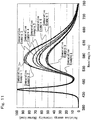
- Fig. 11 shows the emission spectra of Comparative Examples 1 to 9.
- the light emitting devices of Comparative Examples 1 to 9 are the same as the light emitting devices 100 of Examples 1 to 17 except for the fluorescent material 52.
- the second YAG fluorescent material having a composition of (Y, Gd) 3 Al 5 O 12 :Ce is used as the fluorescent material 52.
- Table 3 shows the light emission characteristics of the light emitting devices of Comparative Examples 1 to 9.
- Table 3 Comparative Example 1 Comparative Example 2 Comparative Example 3 Comparative Example 4 Comparative Example 5 Comparative Example 6 Comparative Example 7 Comparative Example 8 Comparative Example 9
- Correlated color temperature Tcp [K] 3964 4010 4109 4200 4343 4348 4653 4700 4735 Deviation Duv 0.007 0.006 0.003 -0.001 -0.001 -0.001 -0.006 -0.007 -0.008
- the light emitting devices of Comparative Examples 1 to 9 all showed general color rendering indexes (Ra) in a range from 68.1 to 73.7.
- the light emitting devices of Comparative Examples 1 to 9 also showed special color rendering indexes (R9) related to the red color of light in a range from -28.2 to -1.3.
- the light emitting device of the present invention can be used in a liquid crystal backlight light source, lighting apparatus, backlight light source for display, flash for a camera, auxiliary light source for videos, etc., and particularly in a lighting apparatus or light source requiring color rendering performance.
Applications Claiming Priority (3)
| Application Number | Priority Date | Filing Date | Title |
|---|---|---|---|
| JP2005174518 | 2005-06-15 | ||
| PCT/JP2006/312026 WO2006135005A1 (ja) | 2005-06-15 | 2006-06-15 | 発光装置 |
| EP06766760.0A EP1895599B1 (de) | 2005-06-15 | 2006-06-15 | Lichtemittierendes bauelement |
Related Parent Applications (2)
| Application Number | Title | Priority Date | Filing Date |
|---|---|---|---|
| EP06766760.0A Division-Into EP1895599B1 (de) | 2005-06-15 | 2006-06-15 | Lichtemittierendes bauelement |
| EP06766760.0A Division EP1895599B1 (de) | 2005-06-15 | 2006-06-15 | Lichtemittierendes bauelement |
Publications (2)
| Publication Number | Publication Date |
|---|---|
| EP3565011A1 true EP3565011A1 (de) | 2019-11-06 |
| EP3565011B1 EP3565011B1 (de) | 2022-03-30 |
Family
ID=37532359
Family Applications (2)
| Application Number | Title | Priority Date | Filing Date |
|---|---|---|---|
| EP19176082.6A Active EP3565011B1 (de) | 2005-06-15 | 2006-06-15 | Lichtemittierende vorrichtung |
| EP06766760.0A Active EP1895599B1 (de) | 2005-06-15 | 2006-06-15 | Lichtemittierendes bauelement |
Family Applications After (1)
| Application Number | Title | Priority Date | Filing Date |
|---|---|---|---|
| EP06766760.0A Active EP1895599B1 (de) | 2005-06-15 | 2006-06-15 | Lichtemittierendes bauelement |
Country Status (7)
| Country | Link |
|---|---|
| US (1) | US8044569B2 (de) |
| EP (2) | EP3565011B1 (de) |
| JP (2) | JP5200537B2 (de) |
| KR (1) | KR101194129B1 (de) |
| CN (1) | CN101194375B (de) |
| TW (1) | TWI413276B (de) |
| WO (1) | WO2006135005A1 (de) |
Families Citing this family (33)
| Publication number | Priority date | Publication date | Assignee | Title |
|---|---|---|---|---|
| US7821023B2 (en) | 2005-01-10 | 2010-10-26 | Cree, Inc. | Solid state lighting component |
| US9793247B2 (en) | 2005-01-10 | 2017-10-17 | Cree, Inc. | Solid state lighting component |
| US9070850B2 (en) | 2007-10-31 | 2015-06-30 | Cree, Inc. | Light emitting diode package and method for fabricating same |
| US9335006B2 (en) | 2006-04-18 | 2016-05-10 | Cree, Inc. | Saturated yellow phosphor converted LED and blue converted red LED |
| US10295147B2 (en) | 2006-11-09 | 2019-05-21 | Cree, Inc. | LED array and method for fabricating same |
| JP2009054633A (ja) * | 2007-08-23 | 2009-03-12 | Stanley Electric Co Ltd | Led照明灯具 |
| JP2012502472A (ja) * | 2008-09-04 | 2012-01-26 | スリーエム イノベイティブ プロパティズ カンパニー | 単色光源 |
| CN102197500A (zh) | 2008-09-04 | 2011-09-21 | 3M创新有限公司 | 具有高纵横比的单色光源 |
| WO2010027650A1 (en) * | 2008-09-04 | 2010-03-11 | 3M Innovative Properties Company | Light source with improved monochromaticity |
| KR20110048580A (ko) * | 2008-09-04 | 2011-05-11 | 쓰리엠 이노베이티브 프로퍼티즈 컴파니 | 광 차단 구성요소를 갖는 광원 |
| CN102197551A (zh) * | 2008-09-04 | 2011-09-21 | 3M创新有限公司 | 由gan ld光泵的散热器上式ⅱ-ⅵ族mqw vcsel |
| US9425172B2 (en) | 2008-10-24 | 2016-08-23 | Cree, Inc. | Light emitter array |
| US8598809B2 (en) | 2009-08-19 | 2013-12-03 | Cree, Inc. | White light color changing solid state lighting and methods |
| US8511851B2 (en) | 2009-12-21 | 2013-08-20 | Cree, Inc. | High CRI adjustable color temperature lighting devices |
| JP5410342B2 (ja) * | 2010-03-12 | 2014-02-05 | 星和電機株式会社 | 発光装置 |
| JP5734581B2 (ja) * | 2010-05-21 | 2015-06-17 | シャープ株式会社 | 半導体発光装置 |
| US9786811B2 (en) | 2011-02-04 | 2017-10-10 | Cree, Inc. | Tilted emission LED array |
| WO2012124267A1 (ja) | 2011-03-15 | 2012-09-20 | 株式会社 東芝 | 白色光源 |
| US10842016B2 (en) | 2011-07-06 | 2020-11-17 | Cree, Inc. | Compact optically efficient solid state light source with integrated thermal management |
| KR101219106B1 (ko) * | 2011-08-01 | 2013-01-11 | 삼성전자주식회사 | 발광소자 패키지 및 그 제조방법 |
| JP6356606B2 (ja) * | 2012-10-04 | 2018-07-11 | 株式会社東芝 | 歯科用照明装置 |
| JP6380826B2 (ja) * | 2013-09-20 | 2018-08-29 | パナソニックIpマネジメント株式会社 | 光源装置 |
| EP3557635B1 (de) * | 2013-10-02 | 2020-05-27 | Glbtech Co. Ltd. | Weisslichtemittierende vorrichtung mit hoher farbausbeute |
| CN103642493A (zh) * | 2013-12-23 | 2014-03-19 | 张书生 | 一种高光效、高稳定性无机发光材料及其制造方法 |
| JP6275829B2 (ja) * | 2014-04-30 | 2018-02-07 | シャープ株式会社 | 発光装置 |
| JP6455817B2 (ja) * | 2014-09-12 | 2019-01-23 | パナソニックIpマネジメント株式会社 | 照明装置 |
| JP2017147290A (ja) * | 2016-02-16 | 2017-08-24 | 岩崎電気株式会社 | Ledユニット、及び照明装置 |
| KR101995000B1 (ko) * | 2016-05-16 | 2019-07-01 | 엘지이노텍 주식회사 | 발광소자 패키지 및 조명장치 |
| EP3460569A4 (de) | 2016-05-19 | 2020-01-08 | LG Innotek Co., Ltd. | Blitzmodul und endgerät damit |
| US10270015B1 (en) | 2017-01-13 | 2019-04-23 | Nichia Corporation | Light-emitting device |
| JP6558378B2 (ja) * | 2017-01-13 | 2019-08-14 | 日亜化学工業株式会社 | 発光装置 |
| US10669479B2 (en) | 2017-02-20 | 2020-06-02 | Panasonic Intellectual Property Management Co., Ltd. | Light-emitting device |
| WO2023107239A1 (en) * | 2021-12-09 | 2023-06-15 | Lumileds Llc | Oxonitridoberyllosilicate phosphors |
Citations (2)
| Publication number | Priority date | Publication date | Assignee | Title |
|---|---|---|---|---|
| JP2003045206A (ja) | 2001-05-24 | 2003-02-14 | Matsushita Electric Ind Co Ltd | 照明光源 |
| WO2004039915A1 (ja) * | 2002-10-16 | 2004-05-13 | Nichia Corporation | 酸窒化物蛍光体及びその製造方法並びにその酸窒化物蛍光体を用いた発光装置 |
Family Cites Families (14)
| Publication number | Priority date | Publication date | Assignee | Title |
|---|---|---|---|---|
| US6613247B1 (en) * | 1996-09-20 | 2003-09-02 | Osram Opto Semiconductors Gmbh | Wavelength-converting casting composition and white light-emitting semiconductor component |
| US6680569B2 (en) * | 1999-02-18 | 2004-01-20 | Lumileds Lighting U.S. Llc | Red-deficiency compensating phosphor light emitting device |
| US6686691B1 (en) * | 1999-09-27 | 2004-02-03 | Lumileds Lighting, U.S., Llc | Tri-color, white light LED lamps |
| US6577073B2 (en) | 2000-05-31 | 2003-06-10 | Matsushita Electric Industrial Co., Ltd. | Led lamp |
| JP4386693B2 (ja) * | 2000-05-31 | 2009-12-16 | パナソニック株式会社 | Ledランプおよびランプユニット |
| CN100430456C (zh) * | 2002-03-22 | 2008-11-05 | 日亚化学工业株式会社 | 氮化物荧光体,其制造方法及发光装置 |
| JP2003318447A (ja) * | 2002-04-24 | 2003-11-07 | Toshiba Lighting & Technology Corp | 発光ダイオードおよびled照明装置 |
| US6717353B1 (en) * | 2002-10-14 | 2004-04-06 | Lumileds Lighting U.S., Llc | Phosphor converted light emitting device |
| JP2004210921A (ja) * | 2002-12-27 | 2004-07-29 | Nichia Chem Ind Ltd | オキシ窒化物蛍光体及びその製造方法並びにそれを用いた発光装置 |
| JP4991026B2 (ja) | 2003-02-26 | 2012-08-01 | 日亜化学工業株式会社 | 発光装置 |
| JP4916651B2 (ja) * | 2003-08-28 | 2012-04-18 | 三菱化学株式会社 | 発光装置及び蛍光体 |
| EP1659335A4 (de) | 2003-08-28 | 2010-05-05 | Mitsubishi Chem Corp | Lichtabgabevorrichtung und -phosphor |
| JP4414821B2 (ja) * | 2004-06-25 | 2010-02-10 | Dowaエレクトロニクス株式会社 | 蛍光体並びに光源およびled |
| JP2006063214A (ja) * | 2004-08-27 | 2006-03-09 | Dowa Mining Co Ltd | 蛍光体及びその製造方法並びに光源 |
-
2006
- 2006-06-15 CN CN2006800203512A patent/CN101194375B/zh active Active
- 2006-06-15 KR KR1020087000992A patent/KR101194129B1/ko active IP Right Grant
- 2006-06-15 TW TW095121443A patent/TWI413276B/zh active
- 2006-06-15 EP EP19176082.6A patent/EP3565011B1/de active Active
- 2006-06-15 EP EP06766760.0A patent/EP1895599B1/de active Active
- 2006-06-15 WO PCT/JP2006/312026 patent/WO2006135005A1/ja active Application Filing
- 2006-06-15 US US11/922,125 patent/US8044569B2/en active Active
- 2006-06-15 JP JP2007521338A patent/JP5200537B2/ja active Active
-
2012
- 2012-09-05 JP JP2012195200A patent/JP5429342B2/ja active Active
Patent Citations (3)
| Publication number | Priority date | Publication date | Assignee | Title |
|---|---|---|---|---|
| JP2003045206A (ja) | 2001-05-24 | 2003-02-14 | Matsushita Electric Ind Co Ltd | 照明光源 |
| WO2004039915A1 (ja) * | 2002-10-16 | 2004-05-13 | Nichia Corporation | 酸窒化物蛍光体及びその製造方法並びにその酸窒化物蛍光体を用いた発光装置 |
| EP1571194A1 (de) * | 2002-10-16 | 2005-09-07 | Nichia Corporation | Oxonitrid-leuchtstoff und verfahren zu dessen herstellung sowie auf dem oxonitrid-leuchtstoff basierende lumineszenzvorrichtung |
Non-Patent Citations (1)
| Title |
|---|
| RAVICHANDRAN D ET AL: "Crystal chemistry and luminescence of the Eu2+-activated alkaline earth aluminate phosphors", DISPLAYS DEVICES, DEMPA PUBLICATIONS, TOKYO, JP, vol. 19, no. 4, 1999, pages 197 - 203, XP029996192, ISSN: 0141-9382, DOI: 10.1016/S0141-9382(98)00050-X * |
Also Published As
| Publication number | Publication date |
|---|---|
| EP1895599A1 (de) | 2008-03-05 |
| US8044569B2 (en) | 2011-10-25 |
| JP5200537B2 (ja) | 2013-06-05 |
| TWI413276B (zh) | 2013-10-21 |
| WO2006135005A1 (ja) | 2006-12-21 |
| KR20080027343A (ko) | 2008-03-26 |
| EP1895599B1 (de) | 2019-09-04 |
| KR101194129B1 (ko) | 2012-10-24 |
| JP2013033971A (ja) | 2013-02-14 |
| TW200711174A (en) | 2007-03-16 |
| EP3565011B1 (de) | 2022-03-30 |
| JP5429342B2 (ja) | 2014-02-26 |
| US20100277054A1 (en) | 2010-11-04 |
| CN101194375B (zh) | 2011-03-23 |
| CN101194375A (zh) | 2008-06-04 |
| EP1895599A4 (de) | 2014-03-19 |
| JPWO2006135005A1 (ja) | 2009-01-08 |
Similar Documents
| Publication | Publication Date | Title |
|---|---|---|
| EP3565011B1 (de) | Lichtemittierende vorrichtung | |
| EP1630877B1 (de) | LED mit fluoreszierendem Stoff | |
| US7854859B2 (en) | Nitride phosphor, method for producing this nitride phosphor, and light emitting device that uses this nitride phosphor | |
| EP1830418B1 (de) | Lichtemittierende Vorrichtung | |
| US7753553B2 (en) | Illumination system comprising color deficiency compensating luminescent material | |
| EP1503428B1 (de) | Lichtemittierendes bauelement mit einer fluoreszenten substanz | |
| JP4559496B2 (ja) | 発光装置 | |
| KR100894372B1 (ko) | 반도체 발광소자와 이를 이용한 발광장치 | |
| TWI492413B (zh) | 發光裝置 | |
| EP2604669B1 (de) | Phosphor und lichtemittierende vorrichtung | |
| JP2004207688A (ja) | 発光装置およびそれを用いた面状光源 | |
| JP6550889B2 (ja) | 発光装置及びその製造方法 |
Legal Events
| Date | Code | Title | Description |
|---|---|---|---|
| PUAI | Public reference made under article 153(3) epc to a published international application that has entered the european phase |
Free format text: ORIGINAL CODE: 0009012 |
|
| STAA | Information on the status of an ep patent application or granted ep patent |
Free format text: STATUS: THE APPLICATION HAS BEEN PUBLISHED |
|
| AC | Divisional application: reference to earlier application |
Ref document number: 1895599 Country of ref document: EP Kind code of ref document: P |
|
| AK | Designated contracting states |
Kind code of ref document: A1 Designated state(s): AT BE BG CH CY CZ DE DK EE ES FI FR GB GR HU IE IS IT LI LT LU LV MC NL PL PT RO SE SI SK TR |
|
| STAA | Information on the status of an ep patent application or granted ep patent |
Free format text: STATUS: REQUEST FOR EXAMINATION WAS MADE |
|
| 17P | Request for examination filed |
Effective date: 20200401 |
|
| RBV | Designated contracting states (corrected) |
Designated state(s): AT BE BG CH CY CZ DE DK EE ES FI FR GB GR HU IE IS IT LI LT LU LV MC NL PL PT RO SE SI SK TR |
|
| GRAP | Despatch of communication of intention to grant a patent |
Free format text: ORIGINAL CODE: EPIDOSNIGR1 |
|
| STAA | Information on the status of an ep patent application or granted ep patent |
Free format text: STATUS: GRANT OF PATENT IS INTENDED |
|
| INTG | Intention to grant announced |
Effective date: 20210909 |
|
| GRAS | Grant fee paid |
Free format text: ORIGINAL CODE: EPIDOSNIGR3 |
|
| GRAJ | Information related to disapproval of communication of intention to grant by the applicant or resumption of examination proceedings by the epo deleted |
Free format text: ORIGINAL CODE: EPIDOSDIGR1 |
|
| GRAL | Information related to payment of fee for publishing/printing deleted |
Free format text: ORIGINAL CODE: EPIDOSDIGR3 |
|
| STAA | Information on the status of an ep patent application or granted ep patent |
Free format text: STATUS: REQUEST FOR EXAMINATION WAS MADE |
|
| GRAP | Despatch of communication of intention to grant a patent |
Free format text: ORIGINAL CODE: EPIDOSNIGR1 |
|
| STAA | Information on the status of an ep patent application or granted ep patent |
Free format text: STATUS: GRANT OF PATENT IS INTENDED |
|
| INTC | Intention to grant announced (deleted) | ||
| INTG | Intention to grant announced |
Effective date: 20220125 |
|
| GRAA | (expected) grant |
Free format text: ORIGINAL CODE: 0009210 |
|
| STAA | Information on the status of an ep patent application or granted ep patent |
Free format text: STATUS: THE PATENT HAS BEEN GRANTED |
|
| AC | Divisional application: reference to earlier application |
Ref document number: 1895599 Country of ref document: EP Kind code of ref document: P |
|
| AK | Designated contracting states |
Kind code of ref document: B1 Designated state(s): AT BE BG CH CY CZ DE DK EE ES FI FR GB GR HU IE IS IT LI LT LU LV MC NL PL PT RO SE SI SK TR |
|
| REG | Reference to a national code |
Ref country code: GB Ref legal event code: FG4D |
|
| REG | Reference to a national code |
Ref country code: CH Ref legal event code: EP |
|
| REG | Reference to a national code |
Ref country code: DE Ref legal event code: R096 Ref document number: 602006060308 Country of ref document: DE |
|
| REG | Reference to a national code |
Ref country code: AT Ref legal event code: REF Ref document number: 1480007 Country of ref document: AT Kind code of ref document: T Effective date: 20220415 |
|
| REG | Reference to a national code |
Ref country code: IE Ref legal event code: FG4D |
|
| REG | Reference to a national code |
Ref country code: NL Ref legal event code: FP |
|
| REG | Reference to a national code |
Ref country code: LT Ref legal event code: MG9D |
|
| PG25 | Lapsed in a contracting state [announced via postgrant information from national office to epo] |
Ref country code: SE Free format text: LAPSE BECAUSE OF FAILURE TO SUBMIT A TRANSLATION OF THE DESCRIPTION OR TO PAY THE FEE WITHIN THE PRESCRIBED TIME-LIMIT Effective date: 20220330 Ref country code: LT Free format text: LAPSE BECAUSE OF FAILURE TO SUBMIT A TRANSLATION OF THE DESCRIPTION OR TO PAY THE FEE WITHIN THE PRESCRIBED TIME-LIMIT Effective date: 20220330 Ref country code: BG Free format text: LAPSE BECAUSE OF FAILURE TO SUBMIT A TRANSLATION OF THE DESCRIPTION OR TO PAY THE FEE WITHIN THE PRESCRIBED TIME-LIMIT Effective date: 20220630 |
|
| REG | Reference to a national code |
Ref country code: AT Ref legal event code: MK05 Ref document number: 1480007 Country of ref document: AT Kind code of ref document: T Effective date: 20220330 |
|
| PG25 | Lapsed in a contracting state [announced via postgrant information from national office to epo] |
Ref country code: LV Free format text: LAPSE BECAUSE OF FAILURE TO SUBMIT A TRANSLATION OF THE DESCRIPTION OR TO PAY THE FEE WITHIN THE PRESCRIBED TIME-LIMIT Effective date: 20220330 Ref country code: GR Free format text: LAPSE BECAUSE OF FAILURE TO SUBMIT A TRANSLATION OF THE DESCRIPTION OR TO PAY THE FEE WITHIN THE PRESCRIBED TIME-LIMIT Effective date: 20220701 Ref country code: FI Free format text: LAPSE BECAUSE OF FAILURE TO SUBMIT A TRANSLATION OF THE DESCRIPTION OR TO PAY THE FEE WITHIN THE PRESCRIBED TIME-LIMIT Effective date: 20220330 |
|
| PG25 | Lapsed in a contracting state [announced via postgrant information from national office to epo] |
Ref country code: SK Free format text: LAPSE BECAUSE OF FAILURE TO SUBMIT A TRANSLATION OF THE DESCRIPTION OR TO PAY THE FEE WITHIN THE PRESCRIBED TIME-LIMIT Effective date: 20220330 Ref country code: RO Free format text: LAPSE BECAUSE OF FAILURE TO SUBMIT A TRANSLATION OF THE DESCRIPTION OR TO PAY THE FEE WITHIN THE PRESCRIBED TIME-LIMIT Effective date: 20220330 Ref country code: PT Free format text: LAPSE BECAUSE OF FAILURE TO SUBMIT A TRANSLATION OF THE DESCRIPTION OR TO PAY THE FEE WITHIN THE PRESCRIBED TIME-LIMIT Effective date: 20220801 Ref country code: ES Free format text: LAPSE BECAUSE OF FAILURE TO SUBMIT A TRANSLATION OF THE DESCRIPTION OR TO PAY THE FEE WITHIN THE PRESCRIBED TIME-LIMIT Effective date: 20220330 Ref country code: EE Free format text: LAPSE BECAUSE OF FAILURE TO SUBMIT A TRANSLATION OF THE DESCRIPTION OR TO PAY THE FEE WITHIN THE PRESCRIBED TIME-LIMIT Effective date: 20220330 Ref country code: CZ Free format text: LAPSE BECAUSE OF FAILURE TO SUBMIT A TRANSLATION OF THE DESCRIPTION OR TO PAY THE FEE WITHIN THE PRESCRIBED TIME-LIMIT Effective date: 20220330 Ref country code: AT Free format text: LAPSE BECAUSE OF FAILURE TO SUBMIT A TRANSLATION OF THE DESCRIPTION OR TO PAY THE FEE WITHIN THE PRESCRIBED TIME-LIMIT Effective date: 20220330 |
|
| PG25 | Lapsed in a contracting state [announced via postgrant information from national office to epo] |
Ref country code: PL Free format text: LAPSE BECAUSE OF FAILURE TO SUBMIT A TRANSLATION OF THE DESCRIPTION OR TO PAY THE FEE WITHIN THE PRESCRIBED TIME-LIMIT Effective date: 20220330 Ref country code: IS Free format text: LAPSE BECAUSE OF FAILURE TO SUBMIT A TRANSLATION OF THE DESCRIPTION OR TO PAY THE FEE WITHIN THE PRESCRIBED TIME-LIMIT Effective date: 20220730 |
|
| REG | Reference to a national code |
Ref country code: DE Ref legal event code: R097 Ref document number: 602006060308 Country of ref document: DE |
|
| PG25 | Lapsed in a contracting state [announced via postgrant information from national office to epo] |
Ref country code: MC Free format text: LAPSE BECAUSE OF FAILURE TO SUBMIT A TRANSLATION OF THE DESCRIPTION OR TO PAY THE FEE WITHIN THE PRESCRIBED TIME-LIMIT Effective date: 20220330 Ref country code: DK Free format text: LAPSE BECAUSE OF FAILURE TO SUBMIT A TRANSLATION OF THE DESCRIPTION OR TO PAY THE FEE WITHIN THE PRESCRIBED TIME-LIMIT Effective date: 20220330 |
|
| REG | Reference to a national code |
Ref country code: CH Ref legal event code: PL |
|
| PLBE | No opposition filed within time limit |
Free format text: ORIGINAL CODE: 0009261 |
|
| STAA | Information on the status of an ep patent application or granted ep patent |
Free format text: STATUS: NO OPPOSITION FILED WITHIN TIME LIMIT |
|
| REG | Reference to a national code |
Ref country code: BE Ref legal event code: MM Effective date: 20220630 |
|
| 26N | No opposition filed |
Effective date: 20230103 |
|
| PG25 | Lapsed in a contracting state [announced via postgrant information from national office to epo] |
Ref country code: LU Free format text: LAPSE BECAUSE OF NON-PAYMENT OF DUE FEES Effective date: 20220615 Ref country code: LI Free format text: LAPSE BECAUSE OF NON-PAYMENT OF DUE FEES Effective date: 20220630 Ref country code: IE Free format text: LAPSE BECAUSE OF NON-PAYMENT OF DUE FEES Effective date: 20220615 Ref country code: CH Free format text: LAPSE BECAUSE OF NON-PAYMENT OF DUE FEES Effective date: 20220630 |
|
| PG25 | Lapsed in a contracting state [announced via postgrant information from national office to epo] |
Ref country code: SI Free format text: LAPSE BECAUSE OF FAILURE TO SUBMIT A TRANSLATION OF THE DESCRIPTION OR TO PAY THE FEE WITHIN THE PRESCRIBED TIME-LIMIT Effective date: 20220330 Ref country code: BE Free format text: LAPSE BECAUSE OF NON-PAYMENT OF DUE FEES Effective date: 20220630 |
|
| P01 | Opt-out of the competence of the unified patent court (upc) registered |
Effective date: 20230522 |
|
| PGFP | Annual fee paid to national office [announced via postgrant information from national office to epo] |
Ref country code: NL Payment date: 20230515 Year of fee payment: 18 Ref country code: IT Payment date: 20230510 Year of fee payment: 18 Ref country code: FR Payment date: 20230510 Year of fee payment: 18 Ref country code: DE Payment date: 20230502 Year of fee payment: 18 |
|
| PGFP | Annual fee paid to national office [announced via postgrant information from national office to epo] |
Ref country code: TR Payment date: 20230615 Year of fee payment: 18 |
|
| PGFP | Annual fee paid to national office [announced via postgrant information from national office to epo] |
Ref country code: GB Payment date: 20230427 Year of fee payment: 18 |
|
| PG25 | Lapsed in a contracting state [announced via postgrant information from national office to epo] |
Ref country code: HU Free format text: LAPSE BECAUSE OF FAILURE TO SUBMIT A TRANSLATION OF THE DESCRIPTION OR TO PAY THE FEE WITHIN THE PRESCRIBED TIME-LIMIT; INVALID AB INITIO Effective date: 20060615 |
|
| PG25 | Lapsed in a contracting state [announced via postgrant information from national office to epo] |
Ref country code: CY Free format text: LAPSE BECAUSE OF FAILURE TO SUBMIT A TRANSLATION OF THE DESCRIPTION OR TO PAY THE FEE WITHIN THE PRESCRIBED TIME-LIMIT Effective date: 20220330 |