EP3553827A1 - Composant à semi-conducteur iii-v sous forme d'empilement - Google Patents
Composant à semi-conducteur iii-v sous forme d'empilement Download PDFInfo
- Publication number
- EP3553827A1 EP3553827A1 EP19000163.6A EP19000163A EP3553827A1 EP 3553827 A1 EP3553827 A1 EP 3553827A1 EP 19000163 A EP19000163 A EP 19000163A EP 3553827 A1 EP3553827 A1 EP 3553827A1
- Authority
- EP
- European Patent Office
- Prior art keywords
- layer
- region
- stack
- iii
- semiconductor device
- Prior art date
- Legal status (The legal status is an assumption and is not a legal conclusion. Google has not performed a legal analysis and makes no representation as to the accuracy of the status listed.)
- Granted
Links
Images

Classifications
-
- H—ELECTRICITY
- H10—SEMICONDUCTOR DEVICES; ELECTRIC SOLID-STATE DEVICES NOT OTHERWISE PROVIDED FOR
- H10D—INORGANIC ELECTRIC SEMICONDUCTOR DEVICES
- H10D8/00—Diodes
- H10D8/422—PN diodes having the PN junctions in mesas
-
- H—ELECTRICITY
- H10—SEMICONDUCTOR DEVICES; ELECTRIC SOLID-STATE DEVICES NOT OTHERWISE PROVIDED FOR
- H10D—INORGANIC ELECTRIC SEMICONDUCTOR DEVICES
- H10D62/00—Semiconductor bodies, or regions thereof, of devices having potential barriers
- H10D62/10—Shapes, relative sizes or dispositions of the regions of the semiconductor bodies; Shapes of the semiconductor bodies
- H10D62/124—Shapes, relative sizes or dispositions of the regions of semiconductor bodies or of junctions between the regions
- H10D62/125—Shapes of junctions between the regions
-
- H—ELECTRICITY
- H10—SEMICONDUCTOR DEVICES; ELECTRIC SOLID-STATE DEVICES NOT OTHERWISE PROVIDED FOR
- H10D—INORGANIC ELECTRIC SEMICONDUCTOR DEVICES
- H10D62/00—Semiconductor bodies, or regions thereof, of devices having potential barriers
- H10D62/10—Shapes, relative sizes or dispositions of the regions of the semiconductor bodies; Shapes of the semiconductor bodies
- H10D62/102—Constructional design considerations for preventing surface leakage or controlling electric field concentration
- H10D62/103—Constructional design considerations for preventing surface leakage or controlling electric field concentration for increasing or controlling the breakdown voltage of reverse-biased devices
- H10D62/104—Constructional design considerations for preventing surface leakage or controlling electric field concentration for increasing or controlling the breakdown voltage of reverse-biased devices having particular shapes of the bodies at or near reverse-biased junctions, e.g. having bevels or moats
-
- H—ELECTRICITY
- H10—SEMICONDUCTOR DEVICES; ELECTRIC SOLID-STATE DEVICES NOT OTHERWISE PROVIDED FOR
- H10D—INORGANIC ELECTRIC SEMICONDUCTOR DEVICES
- H10D62/00—Semiconductor bodies, or regions thereof, of devices having potential barriers
- H10D62/10—Shapes, relative sizes or dispositions of the regions of the semiconductor bodies; Shapes of the semiconductor bodies
- H10D62/117—Shapes of semiconductor bodies
-
- H—ELECTRICITY
- H10—SEMICONDUCTOR DEVICES; ELECTRIC SOLID-STATE DEVICES NOT OTHERWISE PROVIDED FOR
- H10D—INORGANIC ELECTRIC SEMICONDUCTOR DEVICES
- H10D62/00—Semiconductor bodies, or regions thereof, of devices having potential barriers
- H10D62/50—Physical imperfections
- H10D62/53—Physical imperfections the imperfections being within the semiconductor body
-
- H—ELECTRICITY
- H10—SEMICONDUCTOR DEVICES; ELECTRIC SOLID-STATE DEVICES NOT OTHERWISE PROVIDED FOR
- H10D—INORGANIC ELECTRIC SEMICONDUCTOR DEVICES
- H10D62/00—Semiconductor bodies, or regions thereof, of devices having potential barriers
- H10D62/50—Physical imperfections
- H10D62/57—Physical imperfections the imperfections being on the surface of the semiconductor body, e.g. the body having a roughened surface
-
- H—ELECTRICITY
- H10—SEMICONDUCTOR DEVICES; ELECTRIC SOLID-STATE DEVICES NOT OTHERWISE PROVIDED FOR
- H10D—INORGANIC ELECTRIC SEMICONDUCTOR DEVICES
- H10D62/00—Semiconductor bodies, or regions thereof, of devices having potential barriers
- H10D62/60—Impurity distributions or concentrations
-
- H—ELECTRICITY
- H10—SEMICONDUCTOR DEVICES; ELECTRIC SOLID-STATE DEVICES NOT OTHERWISE PROVIDED FOR
- H10D—INORGANIC ELECTRIC SEMICONDUCTOR DEVICES
- H10D62/00—Semiconductor bodies, or regions thereof, of devices having potential barriers
- H10D62/80—Semiconductor bodies, or regions thereof, of devices having potential barriers characterised by the materials
- H10D62/85—Semiconductor bodies, or regions thereof, of devices having potential barriers characterised by the materials being Group III-V materials, e.g. GaAs
-
- H—ELECTRICITY
- H10—SEMICONDUCTOR DEVICES; ELECTRIC SOLID-STATE DEVICES NOT OTHERWISE PROVIDED FOR
- H10D—INORGANIC ELECTRIC SEMICONDUCTOR DEVICES
- H10D8/00—Diodes
-
- H—ELECTRICITY
- H10—SEMICONDUCTOR DEVICES; ELECTRIC SOLID-STATE DEVICES NOT OTHERWISE PROVIDED FOR
- H10D—INORGANIC ELECTRIC SEMICONDUCTOR DEVICES
- H10D8/00—Diodes
- H10D8/01—Manufacture or treatment
- H10D8/043—Manufacture or treatment of planar diodes
-
- H—ELECTRICITY
- H10—SEMICONDUCTOR DEVICES; ELECTRIC SOLID-STATE DEVICES NOT OTHERWISE PROVIDED FOR
- H10D—INORGANIC ELECTRIC SEMICONDUCTOR DEVICES
- H10D8/00—Diodes
- H10D8/60—Schottky-barrier diodes
-
- H—ELECTRICITY
- H10—SEMICONDUCTOR DEVICES; ELECTRIC SOLID-STATE DEVICES NOT OTHERWISE PROVIDED FOR
- H10P—GENERIC PROCESSES OR APPARATUS FOR THE MANUFACTURE OR TREATMENT OF DEVICES COVERED BY CLASS H10
- H10P10/00—Bonding of wafers, substrates or parts of devices
- H10P10/12—Bonding of semiconductor wafers or semiconductor substrates to semiconductor wafers or semiconductor substrates
- H10P10/128—Bonding of semiconductor wafers or semiconductor substrates to semiconductor wafers or semiconductor substrates by direct semiconductor to semiconductor bonding
Definitions
- the invention relates to a stacked III-V semiconductor device.
- GaAs Power Devices by German Ashkinazi, ISBN 965-7094-19-4 , are high voltage resistant semiconductor diodes p + - n - n + and Schottky diodes, high voltage resistant pnip transistors based on GaAs known.
- Chapter 5.3 also describes a mesa process and the coating of side surfaces with a polyimide.
- the object of the invention is to provide a device which further develops the prior art.
- the invention relates to a stacked III-V semiconductor device, comprising a stack having an upper side, a lower side, a side surface connecting the upper side and the lower side, and a longitudinal axis extending through the upper side and the lower side.
- the stack has a p + region with a top, a bottom and a dopant concentration of 5 • 10 18 -5 • 10 20 N / cm 3 , an n - layer with a top and a bottom, a dopant concentration of 10 12 - 10 17 N / cm 3 and a layer thickness of 10 - 300 microns and an n + region with a top side, a bottom side and a dopant concentration of at least 10 19 N / cm 3 .
- the p + region, the n - layer, and the n + region follow each other along the longitudinal axis of the stack in the order named, each formed monolithically and each comprise a GaAs compound or each consist of a GaAs compound.
- the n + region or the p + region is formed as a substrate layer.
- the stack has, in the region of the side surface, a first peripheral, heel-shaped edge and a second circumferential heel-shaped edge, wherein the first edge is formed by the substrate layer, the second edge by the n - layer or one to the n - layer and The p + region adjacent intermediate layer is formed and the first peripheral edge and the second peripheral edge each have a width of at least 10 microns.
- the top and bottom of the stack are rectangular, square or round, for example.
- the layers are preferably produced by means of liquid phase epitaxy or by means of an MOVPE system.
- this has the semiconductor component at least two preferably formed as layers terminal contacts, wherein the terminal contacts are each electrically conductive and have metallic properties.
- connection contact layers preferably consist of metallically conductive semiconductor layers or metal layers or a combination of both.
- the connection contacts provide an electrically low-resistance contact with the directly adjacent doped semiconductor layers ago. Furthermore, it is understood that the connection contacts are preferably connected by means of bonding wires with contact fingers, the so-called pins.
- connection contacts are preferably arranged on an upper side or a lower side of the stack formed from the semiconductor regions or semiconductor layers.
- the circumferential heel-shaped edges are each produced by means of an etching process.
- the depth of the steps that is to say the distance between the top side of the stack and the first edge or between the first edge and the second edge, is preferably controlled over a respective etching time as a function of the etching rate.
- One advantage is that the structuring of the edge improves the device properties.
- the blocking voltages can be increased and suppress the leakage currents at the surface.
- III-V semiconductor diode of the present invention low leakage currents at reverse voltages in a range of 200V-3000V with smaller on-resistances and lower capacitance per area can be easily produced than conventional Si high-blocking diodes or SiC.
- III-V semiconductor diodes can be produced more cost-effectively than comparable high-blocking diodes made of SiC.
- III-V semiconductor diodes according to the invention can be used as freewheeling diodes.
- III-V semiconductor diodes according to the invention in the present case have small turn-on resistances in a range between 1 mOhm and 200 mOhm.
- the capacities per area are in a range between 2 pF and 100 pF.
- III-V semiconductor diode Another advantage of the III-V semiconductor diode according to the invention is a high temperature resistance of up to 300 ° C.
- the III-V semiconductor diodes can also be used in hot environments. In this case, low leakage currents due to the exponential increase with increasing temperature are particularly helpful.
- a first insulation layer produced by implantation is formed.
- the insulation layer is formed for example as an amorphized edge region, wherein the amorphization is achieved for example by implantation of hydrogen ions.
- an insulation layer extends at least along a part of the side surface of the stack.
- an oxide layer is applied to the side surface by means of chemical vapor deposition (CVD).
- the oxide layer preferably has a thickness of 10 ⁇ m -15 ⁇ m or of 20 ⁇ m-30 ⁇ m.
- the semiconductor device comprises a first contact layer and a second contact layer, the second contact layer partially covering the top of the stack so that the top of the stack forms a third circumferential edge of at least 10 ⁇ m width around the second contact layer.
- the first contact layer preferably completely covers the underside of the stack.
- the p + region and the n + region are layered, wherein the layered n + region and the layered p + region are each connected in a materially bonded manner to the n - layer, the layered n + region a layer thickness of 50-675 has the layered p + region has a layer thickness greater than 2 microns, the stacked III-V semiconductor device has a first defect layer with a layer thickness between 0.5 .mu.m and 50 .mu.m and the defect layer is disposed within the n - layer and has a defect concentration in a range between 1 • 10 13 N / cm 3 and 5 • 10 16 N / cm 3 .
- the defect layer can be produced in different ways, for example by implantation or by incorporation of foreign atoms, and recombination of charge carriers is achieved within the defect layer.
- the defects or the recombination centers are achieved by incorporation of chromium.
- a layer thickness of the defect view is a distance of the defect layer to an interface between the n - layer and the p + region at most half the layer thickness of the n - layer.
- the defect layer is preferably not formed within the space charge region.
- the thickness of the n - layer is formed such that the defect layer is spaced from the space charge zone.
- the p + -type region and the n + -type region are formed in layers, wherein the layer-shaped n + region cohesively with the n - layer is connected, between the n - layer and p + layer, a doped Intermediate layer with a layer thickness of 1-50 microns and a dopant concentration of 10 12 -10 17 cm -3 is arranged and the intermediate layer with the n - layer and with the p + layer is firmly bonded.
- the intermediate layer has at least one different dopant concentration compared to the cohesively connected layers.
- the intermediate layer is preferably p-doped and particularly preferably comprises zinc or carbon as dopants.
- the dopant concentration of the p-doped intermediate layer is particularly preferably smaller than the dopant concentration of the p + region, in particular by a factor of 2 up to a factor of 5 orders of magnitude.
- the intermediate layer is n-doped and preferably comprises silicon and / or tin, wherein the dopant concentration of the n-doped intermediate layer is particularly preferably smaller by up to a factor of 100 than the dopant concentration of the n - region.
- the III-V semiconductor diode is monolithic, i. the individual monolithically formed layers are also monolithic to each other.
- the III-V semiconductor diode comprises at least one semiconductor bond.
- semiconductor bond is used synonymously with the term wafer-bond.
- the semiconductor bond in the stacked layer structure consisting of the p + layer, the p-doped intermediate layer, the n - layer and the n + layer, between the n - layer and the p-doped intermediate layer educated.
- the layer structure consisting of a p + layer and the p-doped intermediate layer forms a first partial stack and the layer structure consisting of the n + layer and the n - layer forms a second partial stack.
- the first partial stack is formed in which, starting from a p + layer, the p-doped intermediate layer is produced by means of epitaxy.
- the intermediate layer formed as a p - layer preferably has a doping of less than 10 13 N / cm 3 or a doping of between 10 13 N / cm 3 and 10 15 N / cm 3 .
- the p + layer is thinned before or after bonding by a grinding process to a thickness of between 200 ⁇ m and 500 ⁇ m.
- the first partial stack and the second partial stack are each formed monolithically.
- the second stack is formed in which, starting from an n - substrate, the n - substrate is connected to the second stack by a further wafer bonding process.
- the n - substrate is thinned to the desired thickness.
- the thickness of the n - substrate is in a range between 50 .mu.m to 250 .mu.m.
- the doping of the n'-substrate is in a range between 10 13 N / cm 3 and 10 15 N / cm 3 .
- n - layers can be readily prepared. This eliminates a long epitaxial deposition process. Also, by means of bonding, the number of stacking faults in the thick n - layers can be reduced.
- the defect layer is preferably formed by implanting ions into the surface of the first sub-stack, i. generated in the p-doped intermediate layer.
- the n - substrate has a doping greater than 10 10 N / cm -3 and less than 10 13 N / cm -3 . In that the doping is extremely low, the n - substrate can also be considered as an intrinsic layer.
- n n + layer in a range between 10 18 N / cm 3 and less than 5x10 19 N / cm 3.
- the thinning of the n - substrate preferably takes place by means of a CMP step, ie by means of chemical mechanical polishing.
- an auxiliary layer is applied to the front side of the diode structure. Subsequently, the back of the diode structure leaves thin and placed on a support. In another development, the auxiliary layer is then detached from the front side.
- the surface of the n + substrate and the surface of the p + layer are metallized to electrically connect the semiconductor diode.
- the cathode of the semiconductor diode after the metallization is materially connected to a trained as a heat sink pad.
- the anode is formed on the surface of the diode on the p + layer.
- the: p - - intermediate layer has a thickness between 10 .mu.m to 25 .mu.m and for the n - layer a thickness between 40 .mu.m and 90 .mu.m gives a blocking voltage of about 900 V.
- the: p - - intermediate layer has a thickness between 25 ⁇ m to 35 ⁇ m and for the n - layer a thickness between 40 ⁇ m and 70 ⁇ m results in a blocking voltage of about 1200 V.
- the: p - - intermediate layer has a thickness between 35 microns to 50 microns and the n - layer results in a thickness of between 70 .mu.m and 150 .mu.m and 70 .mu.m a reverse voltage of about 1500 V.
- the diodes in the first to third variants can also be referred to as punch diodes.
- the: p - - intermediate layer has a thickness between 10 .mu.m to 25 .mu.m and for the n - layer has a thickness between 60 .mu.m and 110 .mu.m.
- p - - intermediate layer has a thickness between 10 ⁇ m to 25 ⁇ m and for the n - layer a thickness between 70 ⁇ m and 140.
- the: p - - intermediate layer has a thickness between 35 ⁇ m to 50 ⁇ m and for the n - layer a thickness between 80 ⁇ m and 200 ⁇ m.
- the diodes in the fourth to sixth variants can also be referred to as "non - reach - through” diodes.
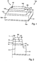
- FIG. 1 schematically shows a perspective view of a first embodiment of a stacked III-V semiconductor device 10 according to the invention.
- the semiconductor device 10 has a stack 100 comprising a plurality of semiconductor layers, with a rectangular upper side 102, a rectangular lower side 104 and a side surface 106 connecting the upper side 102 and the lower side 104.
- the lower side 104 is larger than the upper side 102.
- the side surface 106 consists of four Stair-shaped surfaces, so that form in the region of the side surface 106, a first circumferential paragraph-shaped edge 110 with a first width 120 B1 and a second circumferential paragraph-shaped edge with a second width B2.
- the underside 104 of the stack 100 is completely covered by a first contact layer K1.
- a second contact layer K2 is arranged on the upper side 102 of the semiconductor component 10.
- a first embodiment of the layer sequence of the semiconductor layers of the stack 100 of the semiconductor device 10 is shown in the figure FIG. 2 shown.
- the stack 100 has along a longitudinal axis L a layered p + region 12 with a dopant concentration of 5 ⁇ 10 18 -5 ⁇ 10 20 N / cm 3 , an n - layer with a dopant concentration of 10 12 -10 17 N / cm 3 and a layered n + region with a dopant concentration of at least 10 19 N / cm 3 , each layer having a bottom and a top.
- the p + layer 12 is formed as a substrate with a layer thickness D1, wherein the underside of the p + layer 12 forms the bottom of the stack 100.
- a first part of the top of the p + layer 12 forms the circumferential first edge 110 with the width B1.
- the underside of the n - layer 14 is arranged on a second part of the top of the p + layer 12.
- the n - layer 14 has a layer thickness D2.
- a part of the top of the n - layer forms the circumferential second edge 130 with a width B2.
- the underside of the n + -layer 16 is arranged on a second part of the upper side of the n - -layer 14.
- the n + -layer 16 has a layer thickness D3.
- the top of the n + layer 16 forms the top of the stack 100.
- the underside of the stack 100 is completely covered by the first contact layer K1.
- the second contact layer K2 is formed flat on a central region of the upper side of the stack 100, so that the upper side of the stack 100, in this case the n + -layer 16, forms a third peripheral, stepped edge 130 with a width B3.
- All layers 12, 14 and 16 are monolithic and comprise a GaAs compound or consist of a GaAs compound.
- the stack 100 has a defect layer 30 with a layer thickness D4, wherein the defect layer is arranged within the n - layer 14 and to the underside of the n - layer 14 or the top of the p + layer 12 has a distance A1.
- FIG. 3 In the picture of the FIG. 3 a further embodiment of a layer sequence according to the invention of the III-V semiconductor device is shown. The following are just the differences from the illustration of FIG. 2 explained.
- n + layer 16 is formed as a substrate layer, followed by the n - layer 14, a p- or n-doped intermediate layer 18 with a layer thickness D5 and the p + layer 12.
- an area of the stack 100 adjacent to the side surface is made insulating from the first circumferential edge 110 to an edge adjacent to the top side of the stack 100 and forms a first insulation layer 20.
- a second insulating layer 22, e.g. an oxide layer or a combination of an oxide layer and a nitride layer is deposited by chemical vapor deposition on the side surfaces in the region from the first circumferential edge 110 to an edge adjacent to the top of the stack 100.
- the insulating layer 22 may extend to the surface 102
Landscapes
- Electrodes Of Semiconductors (AREA)
- Recrystallisation Techniques (AREA)
Applications Claiming Priority (1)
| Application Number | Priority Date | Filing Date | Title |
|---|---|---|---|
| DE102018002895.0A DE102018002895A1 (de) | 2018-04-09 | 2018-04-09 | Stapelförmiges III-V-Halbleiterbauelement |
Publications (2)
| Publication Number | Publication Date |
|---|---|
| EP3553827A1 true EP3553827A1 (fr) | 2019-10-16 |
| EP3553827B1 EP3553827B1 (fr) | 2020-07-22 |
Family
ID=66101786
Family Applications (1)
| Application Number | Title | Priority Date | Filing Date |
|---|---|---|---|
| EP19000163.6A Active EP3553827B1 (fr) | 2018-04-09 | 2019-04-01 | Composant à semi-conducteur iii-v sous forme d'empilement |
Country Status (5)
| Country | Link |
|---|---|
| US (1) | US10784381B2 (fr) |
| EP (1) | EP3553827B1 (fr) |
| JP (1) | JP6885619B2 (fr) |
| CN (1) | CN110364565B (fr) |
| DE (1) | DE102018002895A1 (fr) |
Cited By (2)
| Publication number | Priority date | Publication date | Assignee | Title |
|---|---|---|---|---|
| EP3886179A1 (fr) * | 2020-03-20 | 2021-09-29 | AZUR SPACE Solar Power GmbH | Diode empilée à semi-conducteur en ingaas à blocage haut |
| EP3882980A3 (fr) * | 2020-03-20 | 2021-09-29 | AZUR SPACE Solar Power GmbH | Diode empilée de puissance à semi-conducteur iii-v à blocage haut |
Families Citing this family (1)
| Publication number | Priority date | Publication date | Assignee | Title |
|---|---|---|---|---|
| DE102021001116A1 (de) * | 2021-03-02 | 2022-09-08 | Azur Space Solar Power Gmbh | Verfahren zum Durchkontaktieren |
Citations (3)
| Publication number | Priority date | Publication date | Assignee | Title |
|---|---|---|---|---|
| US5213994A (en) * | 1989-05-30 | 1993-05-25 | Motorola, Inc. | Method of making high voltage semiconductor device |
| US20060281263A1 (en) * | 2005-05-20 | 2006-12-14 | Shinya Yamazaki | Semiconductor devices and method of manufacturing them |
| US20170069714A1 (en) * | 2015-09-04 | 2017-03-09 | Kabushiki Kaisha Toshiba | Semiconductor device and method of manufacturing the same |
Family Cites Families (13)
| Publication number | Priority date | Publication date | Assignee | Title |
|---|---|---|---|---|
| JPS4915908B1 (fr) * | 1969-09-02 | 1974-04-18 | ||
| JP2851044B2 (ja) * | 1988-03-30 | 1999-01-27 | 株式会社東芝 | 半導体装置の製造方法 |
| IL101966A (en) * | 1992-05-22 | 1998-04-05 | Ramot Ramatsity Authority For | PROCESS FOR FABRICATING Gallium Arsenide p-i-n STRUCTURE |
| US6054369A (en) | 1997-06-30 | 2000-04-25 | Intersil Corporation | Lifetime control for semiconductor devices |
| JPH11307806A (ja) * | 1998-04-17 | 1999-11-05 | Matsushita Electric Ind Co Ltd | 受光素子及びその製造方法 |
| US20070228505A1 (en) * | 2006-04-04 | 2007-10-04 | Mazzola Michael S | Junction barrier schottky rectifiers having epitaxially grown p+-n junctions and methods of making |
| EP2122670A4 (fr) * | 2006-08-07 | 2013-05-15 | Semi Photonics Co Ltd | Procédé de séparation de puces semi-conductrices |
| US20100213513A1 (en) * | 2009-02-26 | 2010-08-26 | Skyworks Solutions, Inc. | Hyperabrupt Diode Structure And Method For Making Same |
| CN103700712B (zh) * | 2012-09-27 | 2017-05-03 | 比亚迪股份有限公司 | 一种快恢复二极管的结构及其制造方法 |
| CN104952909A (zh) * | 2014-09-03 | 2015-09-30 | 安徽省祁门县黄山电器有限责任公司 | 一种二极管芯片的结终端结构 |
| DE102015208097B4 (de) * | 2015-04-30 | 2022-03-31 | Infineon Technologies Ag | Herstellen einer Halbleitervorrichtung durch Epitaxie |
| DE102015007326B3 (de) * | 2015-06-12 | 2016-07-21 | Azur Space Solar Power Gmbh | Optokoppler |
| JP6611532B2 (ja) * | 2015-09-17 | 2019-11-27 | ローム株式会社 | 半導体装置および半導体装置の製造方法 |
-
2018
- 2018-04-09 DE DE102018002895.0A patent/DE102018002895A1/de not_active Withdrawn
-
2019
- 2019-04-01 EP EP19000163.6A patent/EP3553827B1/fr active Active
- 2019-04-08 JP JP2019073590A patent/JP6885619B2/ja active Active
- 2019-04-09 CN CN201910279531.1A patent/CN110364565B/zh active Active
- 2019-04-09 US US16/379,008 patent/US10784381B2/en active Active
Patent Citations (3)
| Publication number | Priority date | Publication date | Assignee | Title |
|---|---|---|---|---|
| US5213994A (en) * | 1989-05-30 | 1993-05-25 | Motorola, Inc. | Method of making high voltage semiconductor device |
| US20060281263A1 (en) * | 2005-05-20 | 2006-12-14 | Shinya Yamazaki | Semiconductor devices and method of manufacturing them |
| US20170069714A1 (en) * | 2015-09-04 | 2017-03-09 | Kabushiki Kaisha Toshiba | Semiconductor device and method of manufacturing the same |
Non-Patent Citations (2)
| Title |
|---|
| A. KOEL: "Characterization of the temperature dependent behavior of snappy phenomenon by the switching-off of GaAs power diode structures", ADVANCES IN FLUID MECHANICS XI, vol. 1, 1 July 2014 (2014-07-01), Southampton UK, pages 439 - 449, XP055545469, ISSN: 1746-4471, ISBN: 978-1-78466-105-2, DOI: 10.2495/HT140381 * |
| VIKTOR VOITOVICH ET AL: "LPE technology for power GaAs diode structures", ESTONIAN JOURNAL OF ENGINEERING, vol. 16, no. 1, 1 January 2010 (2010-01-01), pages 11 - 22, XP055498749, DOI: 10.3176/eng.2010.1.04 * |
Cited By (3)
| Publication number | Priority date | Publication date | Assignee | Title |
|---|---|---|---|---|
| EP3886179A1 (fr) * | 2020-03-20 | 2021-09-29 | AZUR SPACE Solar Power GmbH | Diode empilée à semi-conducteur en ingaas à blocage haut |
| EP3882980A3 (fr) * | 2020-03-20 | 2021-09-29 | AZUR SPACE Solar Power GmbH | Diode empilée de puissance à semi-conducteur iii-v à blocage haut |
| US12464741B2 (en) | 2020-03-20 | 2025-11-04 | Azur Space Solar Power Gmbh | Stacked high-blocking InGaAs semiconductor power diode |
Also Published As
| Publication number | Publication date |
|---|---|
| US10784381B2 (en) | 2020-09-22 |
| JP6885619B2 (ja) | 2021-06-16 |
| DE102018002895A1 (de) | 2019-10-10 |
| EP3553827B1 (fr) | 2020-07-22 |
| CN110364565B (zh) | 2022-11-01 |
| JP2019186549A (ja) | 2019-10-24 |
| CN110364565A (zh) | 2019-10-22 |
| US20190312151A1 (en) | 2019-10-10 |
Similar Documents
| Publication | Publication Date | Title |
|---|---|---|
| EP3514837B1 (fr) | Diode semi-conductrice iii-v | |
| EP3557632B1 (fr) | Diode semi-conductrice iii-v à base de gaas | |
| EP3379577B1 (fr) | Diode semi-conductrice iii-v à base de gaas | |
| EP3321970B1 (fr) | Diode semi-conductrice iii-v | |
| DE102018214901B4 (de) | Halbleitervorrichtung | |
| DE102014216989B4 (de) | Siliziumcarbid-Halbleitervorrichtung | |
| DE112018003362T5 (de) | Oxid-halbleitereinheit und verfahren zur herstellung einer oxid-halbleitereinheit | |
| EP3503204B1 (fr) | Composant à semi-conducteurs iii-v | |
| DE102011054825B4 (de) | Halbleiterbauelemente und ein Verfahren zum Herstellen von Halbleiterbauelementen | |
| DE102008042170A1 (de) | Siliziumkarbid-Halbleitervorrichtung | |
| EP3522233B1 (fr) | Diode à semi-conduceur iii-v sous forme d'empilement | |
| DE19701189A1 (de) | Halbleiterbauteil | |
| DE102011080258A1 (de) | Super-Junction-Schottky-Oxid-PiN-Diode | |
| EP0760528A2 (fr) | Dispositif semi-conducteur sur base de silicium avec bordure à blocage élevé | |
| EP3553827B1 (fr) | Composant à semi-conducteur iii-v sous forme d'empilement | |
| EP3343636B1 (fr) | Structure semi-conductrice igbt | |
| EP3321972B1 (fr) | Diode schottky empilée | |
| EP4138146A2 (fr) | Diode empilée de puissance à semi-conducteur iii-v à blocage élevé | |
| DE102019003068A1 (de) | Stapelförmige hochsperrende lnGaAS-Halbleiterleistungsdiode | |
| DE102021205424A1 (de) | Halbleitervorrichtung | |
| EP0093866A2 (fr) | Diode Schottky | |
| EP3882980A2 (fr) | Diode empilée de puissance à semi-conducteur iii-v à blocage haut | |
| EP3882979A1 (fr) | Diode empilée de puissance à semi-conducteur iii-v à blocage haut | |
| DE102022107993A1 (de) | Halbleitervorrichtung | |
| DE102020001841A1 (de) | Stapelförmige hochsperrende III-V-Halbleiterleistungsdiode |
Legal Events
| Date | Code | Title | Description |
|---|---|---|---|
| PUAI | Public reference made under article 153(3) epc to a published international application that has entered the european phase |
Free format text: ORIGINAL CODE: 0009012 |
|
| STAA | Information on the status of an ep patent application or granted ep patent |
Free format text: STATUS: THE APPLICATION HAS BEEN PUBLISHED |
|
| STAA | Information on the status of an ep patent application or granted ep patent |
Free format text: STATUS: REQUEST FOR EXAMINATION WAS MADE |
|
| AK | Designated contracting states |
Kind code of ref document: A1 Designated state(s): AL AT BE BG CH CY CZ DE DK EE ES FI FR GB GR HR HU IE IS IT LI LT LU LV MC MK MT NL NO PL PT RO RS SE SI SK SM TR |
|
| AX | Request for extension of the european patent |
Extension state: BA ME |
|
| 17P | Request for examination filed |
Effective date: 20190923 |
|
| RBV | Designated contracting states (corrected) |
Designated state(s): AL AT BE BG CH CY CZ DE DK EE ES FI FR GB GR HR HU IE IS IT LI LT LU LV MC MK MT NL NO PL PT RO RS SE SI SK SM TR |
|
| GRAJ | Information related to disapproval of communication of intention to grant by the applicant or resumption of examination proceedings by the epo deleted |
Free format text: ORIGINAL CODE: EPIDOSDIGR1 |
|
| GRAP | Despatch of communication of intention to grant a patent |
Free format text: ORIGINAL CODE: EPIDOSNIGR1 |
|
| GRAP | Despatch of communication of intention to grant a patent |
Free format text: ORIGINAL CODE: EPIDOSNIGR1 |
|
| RIC1 | Information provided on ipc code assigned before grant |
Ipc: H01L 29/36 20060101ALN20200312BHEP Ipc: H01L 29/20 20060101ALI20200312BHEP Ipc: H01L 21/18 20060101ALN20200312BHEP Ipc: H01L 29/06 20060101ALI20200312BHEP Ipc: H01L 29/861 20060101AFI20200312BHEP Ipc: H01L 29/34 20060101ALI20200312BHEP Ipc: H01L 29/32 20060101ALI20200312BHEP Ipc: H01L 21/329 20060101ALI20200312BHEP |
|
| STAA | Information on the status of an ep patent application or granted ep patent |
Free format text: STATUS: GRANT OF PATENT IS INTENDED |
|
| INTG | Intention to grant announced |
Effective date: 20200416 |
|
| RIC1 | Information provided on ipc code assigned before grant |
Ipc: H01L 21/329 20060101ALI20200406BHEP Ipc: H01L 29/06 20060101ALI20200406BHEP Ipc: H01L 29/861 20060101AFI20200406BHEP Ipc: H01L 29/34 20060101ALI20200406BHEP Ipc: H01L 21/18 20060101ALN20200406BHEP Ipc: H01L 29/20 20060101ALI20200406BHEP Ipc: H01L 29/36 20060101ALN20200406BHEP Ipc: H01L 29/32 20060101ALI20200406BHEP |
|
| GRAS | Grant fee paid |
Free format text: ORIGINAL CODE: EPIDOSNIGR3 |
|
| GRAA | (expected) grant |
Free format text: ORIGINAL CODE: 0009210 |
|
| STAA | Information on the status of an ep patent application or granted ep patent |
Free format text: STATUS: THE PATENT HAS BEEN GRANTED |
|
| AK | Designated contracting states |
Kind code of ref document: B1 Designated state(s): AL AT BE BG CH CY CZ DE DK EE ES FI FR GB GR HR HU IE IS IT LI LT LU LV MC MK MT NL NO PL PT RO RS SE SI SK SM TR |
|
| REG | Reference to a national code |
Ref country code: GB Ref legal event code: FG4D Free format text: NOT ENGLISH |
|
| REG | Reference to a national code |
Ref country code: CH Ref legal event code: EP |
|
| REG | Reference to a national code |
Ref country code: DE Ref legal event code: R096 Ref document number: 502019000090 Country of ref document: DE |
|
| REG | Reference to a national code |
Ref country code: AT Ref legal event code: REF Ref document number: 1294221 Country of ref document: AT Kind code of ref document: T Effective date: 20200815 |
|
| REG | Reference to a national code |
Ref country code: IE Ref legal event code: FG4D Free format text: LANGUAGE OF EP DOCUMENT: GERMAN |
|
| REG | Reference to a national code |
Ref country code: CH Ref legal event code: NV Representative=s name: KIRKER AND CIE S.A., CH |
|
| REG | Reference to a national code |
Ref country code: LT Ref legal event code: MG4D |
|
| PG25 | Lapsed in a contracting state [announced via postgrant information from national office to epo] |
Ref country code: ES Free format text: LAPSE BECAUSE OF FAILURE TO SUBMIT A TRANSLATION OF THE DESCRIPTION OR TO PAY THE FEE WITHIN THE PRESCRIBED TIME-LIMIT Effective date: 20200722 Ref country code: BG Free format text: LAPSE BECAUSE OF FAILURE TO SUBMIT A TRANSLATION OF THE DESCRIPTION OR TO PAY THE FEE WITHIN THE PRESCRIBED TIME-LIMIT Effective date: 20201022 Ref country code: GR Free format text: LAPSE BECAUSE OF FAILURE TO SUBMIT A TRANSLATION OF THE DESCRIPTION OR TO PAY THE FEE WITHIN THE PRESCRIBED TIME-LIMIT Effective date: 20201023 Ref country code: NO Free format text: LAPSE BECAUSE OF FAILURE TO SUBMIT A TRANSLATION OF THE DESCRIPTION OR TO PAY THE FEE WITHIN THE PRESCRIBED TIME-LIMIT Effective date: 20201022 Ref country code: LT Free format text: LAPSE BECAUSE OF FAILURE TO SUBMIT A TRANSLATION OF THE DESCRIPTION OR TO PAY THE FEE WITHIN THE PRESCRIBED TIME-LIMIT Effective date: 20200722 Ref country code: FI Free format text: LAPSE BECAUSE OF FAILURE TO SUBMIT A TRANSLATION OF THE DESCRIPTION OR TO PAY THE FEE WITHIN THE PRESCRIBED TIME-LIMIT Effective date: 20200722 Ref country code: PT Free format text: LAPSE BECAUSE OF FAILURE TO SUBMIT A TRANSLATION OF THE DESCRIPTION OR TO PAY THE FEE WITHIN THE PRESCRIBED TIME-LIMIT Effective date: 20201123 Ref country code: SE Free format text: LAPSE BECAUSE OF FAILURE TO SUBMIT A TRANSLATION OF THE DESCRIPTION OR TO PAY THE FEE WITHIN THE PRESCRIBED TIME-LIMIT Effective date: 20200722 Ref country code: HR Free format text: LAPSE BECAUSE OF FAILURE TO SUBMIT A TRANSLATION OF THE DESCRIPTION OR TO PAY THE FEE WITHIN THE PRESCRIBED TIME-LIMIT Effective date: 20200722 |
|
| PG25 | Lapsed in a contracting state [announced via postgrant information from national office to epo] |
Ref country code: LV Free format text: LAPSE BECAUSE OF FAILURE TO SUBMIT A TRANSLATION OF THE DESCRIPTION OR TO PAY THE FEE WITHIN THE PRESCRIBED TIME-LIMIT Effective date: 20200722 Ref country code: PL Free format text: LAPSE BECAUSE OF FAILURE TO SUBMIT A TRANSLATION OF THE DESCRIPTION OR TO PAY THE FEE WITHIN THE PRESCRIBED TIME-LIMIT Effective date: 20200722 Ref country code: RS Free format text: LAPSE BECAUSE OF FAILURE TO SUBMIT A TRANSLATION OF THE DESCRIPTION OR TO PAY THE FEE WITHIN THE PRESCRIBED TIME-LIMIT Effective date: 20200722 Ref country code: IS Free format text: LAPSE BECAUSE OF FAILURE TO SUBMIT A TRANSLATION OF THE DESCRIPTION OR TO PAY THE FEE WITHIN THE PRESCRIBED TIME-LIMIT Effective date: 20201122 |
|
| PG25 | Lapsed in a contracting state [announced via postgrant information from national office to epo] |
Ref country code: NL Free format text: LAPSE BECAUSE OF FAILURE TO SUBMIT A TRANSLATION OF THE DESCRIPTION OR TO PAY THE FEE WITHIN THE PRESCRIBED TIME-LIMIT Effective date: 20200722 |
|
| REG | Reference to a national code |
Ref country code: DE Ref legal event code: R097 Ref document number: 502019000090 Country of ref document: DE |
|
| PG25 | Lapsed in a contracting state [announced via postgrant information from national office to epo] |
Ref country code: RO Free format text: LAPSE BECAUSE OF FAILURE TO SUBMIT A TRANSLATION OF THE DESCRIPTION OR TO PAY THE FEE WITHIN THE PRESCRIBED TIME-LIMIT Effective date: 20200722 Ref country code: DK Free format text: LAPSE BECAUSE OF FAILURE TO SUBMIT A TRANSLATION OF THE DESCRIPTION OR TO PAY THE FEE WITHIN THE PRESCRIBED TIME-LIMIT Effective date: 20200722 Ref country code: CZ Free format text: LAPSE BECAUSE OF FAILURE TO SUBMIT A TRANSLATION OF THE DESCRIPTION OR TO PAY THE FEE WITHIN THE PRESCRIBED TIME-LIMIT Effective date: 20200722 Ref country code: EE Free format text: LAPSE BECAUSE OF FAILURE TO SUBMIT A TRANSLATION OF THE DESCRIPTION OR TO PAY THE FEE WITHIN THE PRESCRIBED TIME-LIMIT Effective date: 20200722 Ref country code: SM Free format text: LAPSE BECAUSE OF FAILURE TO SUBMIT A TRANSLATION OF THE DESCRIPTION OR TO PAY THE FEE WITHIN THE PRESCRIBED TIME-LIMIT Effective date: 20200722 Ref country code: IT Free format text: LAPSE BECAUSE OF FAILURE TO SUBMIT A TRANSLATION OF THE DESCRIPTION OR TO PAY THE FEE WITHIN THE PRESCRIBED TIME-LIMIT Effective date: 20200722 |
|
| PLBE | No opposition filed within time limit |
Free format text: ORIGINAL CODE: 0009261 |
|
| STAA | Information on the status of an ep patent application or granted ep patent |
Free format text: STATUS: NO OPPOSITION FILED WITHIN TIME LIMIT |
|
| PG25 | Lapsed in a contracting state [announced via postgrant information from national office to epo] |
Ref country code: AL Free format text: LAPSE BECAUSE OF FAILURE TO SUBMIT A TRANSLATION OF THE DESCRIPTION OR TO PAY THE FEE WITHIN THE PRESCRIBED TIME-LIMIT Effective date: 20200722 |
|
| 26N | No opposition filed |
Effective date: 20210423 |
|
| PG25 | Lapsed in a contracting state [announced via postgrant information from national office to epo] |
Ref country code: SK Free format text: LAPSE BECAUSE OF FAILURE TO SUBMIT A TRANSLATION OF THE DESCRIPTION OR TO PAY THE FEE WITHIN THE PRESCRIBED TIME-LIMIT Effective date: 20200722 |
|
| PG25 | Lapsed in a contracting state [announced via postgrant information from national office to epo] |
Ref country code: SI Free format text: LAPSE BECAUSE OF FAILURE TO SUBMIT A TRANSLATION OF THE DESCRIPTION OR TO PAY THE FEE WITHIN THE PRESCRIBED TIME-LIMIT Effective date: 20200722 |
|
| REG | Reference to a national code |
Ref country code: NL Ref legal event code: MP Effective date: 20200722 |
|
| PG25 | Lapsed in a contracting state [announced via postgrant information from national office to epo] |
Ref country code: MC Free format text: LAPSE BECAUSE OF FAILURE TO SUBMIT A TRANSLATION OF THE DESCRIPTION OR TO PAY THE FEE WITHIN THE PRESCRIBED TIME-LIMIT Effective date: 20200722 |
|
| PG25 | Lapsed in a contracting state [announced via postgrant information from national office to epo] |
Ref country code: LU Free format text: LAPSE BECAUSE OF NON-PAYMENT OF DUE FEES Effective date: 20210401 |
|
| PG25 | Lapsed in a contracting state [announced via postgrant information from national office to epo] |
Ref country code: IE Free format text: LAPSE BECAUSE OF NON-PAYMENT OF DUE FEES Effective date: 20210401 |
|
| PG25 | Lapsed in a contracting state [announced via postgrant information from national office to epo] |
Ref country code: IS Free format text: LAPSE BECAUSE OF FAILURE TO SUBMIT A TRANSLATION OF THE DESCRIPTION OR TO PAY THE FEE WITHIN THE PRESCRIBED TIME-LIMIT Effective date: 20201122 |
|
| PG25 | Lapsed in a contracting state [announced via postgrant information from national office to epo] |
Ref country code: CY Free format text: LAPSE BECAUSE OF FAILURE TO SUBMIT A TRANSLATION OF THE DESCRIPTION OR TO PAY THE FEE WITHIN THE PRESCRIBED TIME-LIMIT Effective date: 20200722 |
|
| PG25 | Lapsed in a contracting state [announced via postgrant information from national office to epo] |
Ref country code: HU Free format text: LAPSE BECAUSE OF FAILURE TO SUBMIT A TRANSLATION OF THE DESCRIPTION OR TO PAY THE FEE WITHIN THE PRESCRIBED TIME-LIMIT; INVALID AB INITIO Effective date: 20190401 |
|
| PG25 | Lapsed in a contracting state [announced via postgrant information from national office to epo] |
Ref country code: MK Free format text: LAPSE BECAUSE OF FAILURE TO SUBMIT A TRANSLATION OF THE DESCRIPTION OR TO PAY THE FEE WITHIN THE PRESCRIBED TIME-LIMIT Effective date: 20200722 |
|
| PG25 | Lapsed in a contracting state [announced via postgrant information from national office to epo] |
Ref country code: MT Free format text: LAPSE BECAUSE OF FAILURE TO SUBMIT A TRANSLATION OF THE DESCRIPTION OR TO PAY THE FEE WITHIN THE PRESCRIBED TIME-LIMIT Effective date: 20200722 |
|
| REG | Reference to a national code |
Ref country code: DE Ref legal event code: R079 Ref document number: 502019000090 Country of ref document: DE Free format text: PREVIOUS MAIN CLASS: H01L0029861000 Ipc: H10D0008000000 |
|
| REG | Reference to a national code |
Ref country code: AT Ref legal event code: MM01 Ref document number: 1294221 Country of ref document: AT Kind code of ref document: T Effective date: 20240401 |
|
| PGFP | Annual fee paid to national office [announced via postgrant information from national office to epo] |
Ref country code: DE Payment date: 20250422 Year of fee payment: 7 |
|
| PGFP | Annual fee paid to national office [announced via postgrant information from national office to epo] |
Ref country code: GB Payment date: 20250423 Year of fee payment: 7 |
|
| PGFP | Annual fee paid to national office [announced via postgrant information from national office to epo] |
Ref country code: BE Payment date: 20250418 Year of fee payment: 7 |
|
| PGFP | Annual fee paid to national office [announced via postgrant information from national office to epo] |
Ref country code: FR Payment date: 20250423 Year of fee payment: 7 |
|
| PGFP | Annual fee paid to national office [announced via postgrant information from national office to epo] |
Ref country code: CH Payment date: 20250501 Year of fee payment: 7 |
|
| PG25 | Lapsed in a contracting state [announced via postgrant information from national office to epo] |
Ref country code: AT Free format text: LAPSE BECAUSE OF NON-PAYMENT OF DUE FEES Effective date: 20240401 |
|
| PG25 | Lapsed in a contracting state [announced via postgrant information from national office to epo] |
Ref country code: TR Free format text: LAPSE BECAUSE OF FAILURE TO SUBMIT A TRANSLATION OF THE DESCRIPTION OR TO PAY THE FEE WITHIN THE PRESCRIBED TIME-LIMIT Effective date: 20200722 |
|
| PGFP | Annual fee paid to national office [announced via postgrant information from national office to epo] |
Ref country code: AT Payment date: 20260410 Year of fee payment: 5 |