EP3553827A1 - Stacked iii-v semi-conductor device - Google Patents
Stacked iii-v semi-conductor device Download PDFInfo
- Publication number
- EP3553827A1 EP3553827A1 EP19000163.6A EP19000163A EP3553827A1 EP 3553827 A1 EP3553827 A1 EP 3553827A1 EP 19000163 A EP19000163 A EP 19000163A EP 3553827 A1 EP3553827 A1 EP 3553827A1
- Authority
- EP
- European Patent Office
- Prior art keywords
- layer
- region
- stack
- iii
- semiconductor device
- Prior art date
- Legal status (The legal status is an assumption and is not a legal conclusion. Google has not performed a legal analysis and makes no representation as to the accuracy of the status listed.)
- Granted
Links
- 239000004065 semiconductor Substances 0.000 title claims abstract description 50
- 239000000758 substrate Substances 0.000 claims abstract description 19
- 229910001218 Gallium arsenide Inorganic materials 0.000 claims abstract description 9
- -1 GaAs compound Chemical class 0.000 claims abstract description 7
- 230000002093 peripheral effect Effects 0.000 claims abstract description 7
- 230000007547 defect Effects 0.000 claims description 17
- 239000002019 doping agent Substances 0.000 claims description 17
- 238000002513 implantation Methods 0.000 claims description 6
- 238000009413 insulation Methods 0.000 claims description 5
- 239000010410 layer Substances 0.000 description 145
- 238000000034 method Methods 0.000 description 5
- 230000000903 blocking effect Effects 0.000 description 4
- 238000005229 chemical vapour deposition Methods 0.000 description 3
- 238000005530 etching Methods 0.000 description 3
- 238000000407 epitaxy Methods 0.000 description 2
- 238000010348 incorporation Methods 0.000 description 2
- 238000005215 recombination Methods 0.000 description 2
- 230000006798 recombination Effects 0.000 description 2
- 229910052710 silicon Inorganic materials 0.000 description 2
- 239000010703 silicon Substances 0.000 description 2
- OKTJSMMVPCPJKN-UHFFFAOYSA-N Carbon Chemical compound [C] OKTJSMMVPCPJKN-UHFFFAOYSA-N 0.000 description 1
- VYZAMTAEIAYCRO-UHFFFAOYSA-N Chromium Chemical compound [Cr] VYZAMTAEIAYCRO-UHFFFAOYSA-N 0.000 description 1
- 239000004642 Polyimide Substances 0.000 description 1
- ATJFFYVFTNAWJD-UHFFFAOYSA-N Tin Chemical compound [Sn] ATJFFYVFTNAWJD-UHFFFAOYSA-N 0.000 description 1
- HCHKCACWOHOZIP-UHFFFAOYSA-N Zinc Chemical compound [Zn] HCHKCACWOHOZIP-UHFFFAOYSA-N 0.000 description 1
- 238000005280 amorphization Methods 0.000 description 1
- 229910052799 carbon Inorganic materials 0.000 description 1
- 239000002800 charge carrier Substances 0.000 description 1
- 229910052804 chromium Inorganic materials 0.000 description 1
- 239000011651 chromium Substances 0.000 description 1
- 239000011248 coating agent Substances 0.000 description 1
- 238000000576 coating method Methods 0.000 description 1
- 230000001419 dependent effect Effects 0.000 description 1
- 238000005137 deposition process Methods 0.000 description 1
- 229910052739 hydrogen Inorganic materials 0.000 description 1
- 239000001257 hydrogen Substances 0.000 description 1
- 239000011229 interlayer Substances 0.000 description 1
- 238000011835 investigation Methods 0.000 description 1
- 150000002500 ions Chemical class 0.000 description 1
- 238000004943 liquid phase epitaxy Methods 0.000 description 1
- 229910052751 metal Inorganic materials 0.000 description 1
- 239000002184 metal Substances 0.000 description 1
- 238000002488 metal-organic chemical vapour deposition Methods 0.000 description 1
- 238000001465 metallisation Methods 0.000 description 1
- 150000004767 nitrides Chemical class 0.000 description 1
- 238000005498 polishing Methods 0.000 description 1
- 229920001721 polyimide Polymers 0.000 description 1
- 239000000126 substance Substances 0.000 description 1
- 229910052725 zinc Inorganic materials 0.000 description 1
- 239000011701 zinc Substances 0.000 description 1
Images

Classifications
-
- H—ELECTRICITY
- H01—ELECTRIC ELEMENTS
- H01L—SEMICONDUCTOR DEVICES NOT COVERED BY CLASS H10
- H01L29/00—Semiconductor devices specially adapted for rectifying, amplifying, oscillating or switching and having potential barriers; Capacitors or resistors having potential barriers, e.g. a PN-junction depletion layer or carrier concentration layer; Details of semiconductor bodies or of electrodes thereof ; Multistep manufacturing processes therefor
- H01L29/66—Types of semiconductor device ; Multistep manufacturing processes therefor
- H01L29/86—Types of semiconductor device ; Multistep manufacturing processes therefor controllable only by variation of the electric current supplied, or only the electric potential applied, to one or more of the electrodes carrying the current to be rectified, amplified, oscillated or switched
- H01L29/861—Diodes
- H01L29/8613—Mesa PN junction diodes
-
- H—ELECTRICITY
- H01—ELECTRIC ELEMENTS
- H01L—SEMICONDUCTOR DEVICES NOT COVERED BY CLASS H10
- H01L29/00—Semiconductor devices specially adapted for rectifying, amplifying, oscillating or switching and having potential barriers; Capacitors or resistors having potential barriers, e.g. a PN-junction depletion layer or carrier concentration layer; Details of semiconductor bodies or of electrodes thereof ; Multistep manufacturing processes therefor
- H01L29/02—Semiconductor bodies ; Multistep manufacturing processes therefor
- H01L29/06—Semiconductor bodies ; Multistep manufacturing processes therefor characterised by their shape; characterised by the shapes, relative sizes, or dispositions of the semiconductor regions ; characterised by the concentration or distribution of impurities within semiconductor regions
- H01L29/0603—Semiconductor bodies ; Multistep manufacturing processes therefor characterised by their shape; characterised by the shapes, relative sizes, or dispositions of the semiconductor regions ; characterised by the concentration or distribution of impurities within semiconductor regions characterised by particular constructional design considerations, e.g. for preventing surface leakage, for controlling electric field concentration or for internal isolations regions
- H01L29/0607—Semiconductor bodies ; Multistep manufacturing processes therefor characterised by their shape; characterised by the shapes, relative sizes, or dispositions of the semiconductor regions ; characterised by the concentration or distribution of impurities within semiconductor regions characterised by particular constructional design considerations, e.g. for preventing surface leakage, for controlling electric field concentration or for internal isolations regions for preventing surface leakage or controlling electric field concentration
-
- H—ELECTRICITY
- H01—ELECTRIC ELEMENTS
- H01L—SEMICONDUCTOR DEVICES NOT COVERED BY CLASS H10
- H01L29/00—Semiconductor devices specially adapted for rectifying, amplifying, oscillating or switching and having potential barriers; Capacitors or resistors having potential barriers, e.g. a PN-junction depletion layer or carrier concentration layer; Details of semiconductor bodies or of electrodes thereof ; Multistep manufacturing processes therefor
- H01L29/02—Semiconductor bodies ; Multistep manufacturing processes therefor
- H01L29/06—Semiconductor bodies ; Multistep manufacturing processes therefor characterised by their shape; characterised by the shapes, relative sizes, or dispositions of the semiconductor regions ; characterised by the concentration or distribution of impurities within semiconductor regions
- H01L29/0657—Semiconductor bodies ; Multistep manufacturing processes therefor characterised by their shape; characterised by the shapes, relative sizes, or dispositions of the semiconductor regions ; characterised by the concentration or distribution of impurities within semiconductor regions characterised by the shape of the body
- H01L29/0661—Semiconductor bodies ; Multistep manufacturing processes therefor characterised by their shape; characterised by the shapes, relative sizes, or dispositions of the semiconductor regions ; characterised by the concentration or distribution of impurities within semiconductor regions characterised by the shape of the body specially adapted for altering the breakdown voltage by removing semiconductor material at, or in the neighbourhood of, a reverse biased junction, e.g. by bevelling, moat etching, depletion etching
-
- H—ELECTRICITY
- H01—ELECTRIC ELEMENTS
- H01L—SEMICONDUCTOR DEVICES NOT COVERED BY CLASS H10
- H01L29/00—Semiconductor devices specially adapted for rectifying, amplifying, oscillating or switching and having potential barriers; Capacitors or resistors having potential barriers, e.g. a PN-junction depletion layer or carrier concentration layer; Details of semiconductor bodies or of electrodes thereof ; Multistep manufacturing processes therefor
- H01L29/02—Semiconductor bodies ; Multistep manufacturing processes therefor
- H01L29/06—Semiconductor bodies ; Multistep manufacturing processes therefor characterised by their shape; characterised by the shapes, relative sizes, or dispositions of the semiconductor regions ; characterised by the concentration or distribution of impurities within semiconductor regions
- H01L29/0684—Semiconductor bodies ; Multistep manufacturing processes therefor characterised by their shape; characterised by the shapes, relative sizes, or dispositions of the semiconductor regions ; characterised by the concentration or distribution of impurities within semiconductor regions characterised by the shape, relative sizes or dispositions of the semiconductor regions or junctions between the regions
- H01L29/0688—Semiconductor bodies ; Multistep manufacturing processes therefor characterised by their shape; characterised by the shapes, relative sizes, or dispositions of the semiconductor regions ; characterised by the concentration or distribution of impurities within semiconductor regions characterised by the shape, relative sizes or dispositions of the semiconductor regions or junctions between the regions characterised by the particular shape of a junction between semiconductor regions
-
- H—ELECTRICITY
- H01—ELECTRIC ELEMENTS
- H01L—SEMICONDUCTOR DEVICES NOT COVERED BY CLASS H10
- H01L29/00—Semiconductor devices specially adapted for rectifying, amplifying, oscillating or switching and having potential barriers; Capacitors or resistors having potential barriers, e.g. a PN-junction depletion layer or carrier concentration layer; Details of semiconductor bodies or of electrodes thereof ; Multistep manufacturing processes therefor
- H01L29/02—Semiconductor bodies ; Multistep manufacturing processes therefor
- H01L29/12—Semiconductor bodies ; Multistep manufacturing processes therefor characterised by the materials of which they are formed
- H01L29/20—Semiconductor bodies ; Multistep manufacturing processes therefor characterised by the materials of which they are formed including, apart from doping materials or other impurities, only AIIIBV compounds
-
- H—ELECTRICITY
- H01—ELECTRIC ELEMENTS
- H01L—SEMICONDUCTOR DEVICES NOT COVERED BY CLASS H10
- H01L29/00—Semiconductor devices specially adapted for rectifying, amplifying, oscillating or switching and having potential barriers; Capacitors or resistors having potential barriers, e.g. a PN-junction depletion layer or carrier concentration layer; Details of semiconductor bodies or of electrodes thereof ; Multistep manufacturing processes therefor
- H01L29/02—Semiconductor bodies ; Multistep manufacturing processes therefor
- H01L29/30—Semiconductor bodies ; Multistep manufacturing processes therefor characterised by physical imperfections; having polished or roughened surface
- H01L29/32—Semiconductor bodies ; Multistep manufacturing processes therefor characterised by physical imperfections; having polished or roughened surface the imperfections being within the semiconductor body
-
- H—ELECTRICITY
- H01—ELECTRIC ELEMENTS
- H01L—SEMICONDUCTOR DEVICES NOT COVERED BY CLASS H10
- H01L29/00—Semiconductor devices specially adapted for rectifying, amplifying, oscillating or switching and having potential barriers; Capacitors or resistors having potential barriers, e.g. a PN-junction depletion layer or carrier concentration layer; Details of semiconductor bodies or of electrodes thereof ; Multistep manufacturing processes therefor
- H01L29/02—Semiconductor bodies ; Multistep manufacturing processes therefor
- H01L29/30—Semiconductor bodies ; Multistep manufacturing processes therefor characterised by physical imperfections; having polished or roughened surface
- H01L29/34—Semiconductor bodies ; Multistep manufacturing processes therefor characterised by physical imperfections; having polished or roughened surface the imperfections being on the surface
-
- H—ELECTRICITY
- H01—ELECTRIC ELEMENTS
- H01L—SEMICONDUCTOR DEVICES NOT COVERED BY CLASS H10
- H01L29/00—Semiconductor devices specially adapted for rectifying, amplifying, oscillating or switching and having potential barriers; Capacitors or resistors having potential barriers, e.g. a PN-junction depletion layer or carrier concentration layer; Details of semiconductor bodies or of electrodes thereof ; Multistep manufacturing processes therefor
- H01L29/66—Types of semiconductor device ; Multistep manufacturing processes therefor
- H01L29/66007—Multistep manufacturing processes
- H01L29/66075—Multistep manufacturing processes of devices having semiconductor bodies comprising group 14 or group 13/15 materials
- H01L29/66083—Multistep manufacturing processes of devices having semiconductor bodies comprising group 14 or group 13/15 materials the devices being controllable only by variation of the electric current supplied or the electric potential applied, to one or more of the electrodes carrying the current to be rectified, amplified, oscillated or switched, e.g. two-terminal devices
- H01L29/66196—Multistep manufacturing processes of devices having semiconductor bodies comprising group 14 or group 13/15 materials the devices being controllable only by variation of the electric current supplied or the electric potential applied, to one or more of the electrodes carrying the current to be rectified, amplified, oscillated or switched, e.g. two-terminal devices with an active layer made of a group 13/15 material
- H01L29/66204—Diodes
-
- H—ELECTRICITY
- H01—ELECTRIC ELEMENTS
- H01L—SEMICONDUCTOR DEVICES NOT COVERED BY CLASS H10
- H01L29/00—Semiconductor devices specially adapted for rectifying, amplifying, oscillating or switching and having potential barriers; Capacitors or resistors having potential barriers, e.g. a PN-junction depletion layer or carrier concentration layer; Details of semiconductor bodies or of electrodes thereof ; Multistep manufacturing processes therefor
- H01L29/66—Types of semiconductor device ; Multistep manufacturing processes therefor
- H01L29/86—Types of semiconductor device ; Multistep manufacturing processes therefor controllable only by variation of the electric current supplied, or only the electric potential applied, to one or more of the electrodes carrying the current to be rectified, amplified, oscillated or switched
- H01L29/861—Diodes
- H01L29/872—Schottky diodes
-
- H—ELECTRICITY
- H01—ELECTRIC ELEMENTS
- H01L—SEMICONDUCTOR DEVICES NOT COVERED BY CLASS H10
- H01L21/00—Processes or apparatus adapted for the manufacture or treatment of semiconductor or solid state devices or of parts thereof
- H01L21/02—Manufacture or treatment of semiconductor devices or of parts thereof
- H01L21/04—Manufacture or treatment of semiconductor devices or of parts thereof the devices having potential barriers, e.g. a PN junction, depletion layer or carrier concentration layer
- H01L21/18—Manufacture or treatment of semiconductor devices or of parts thereof the devices having potential barriers, e.g. a PN junction, depletion layer or carrier concentration layer the devices having semiconductor bodies comprising elements of Group IV of the Periodic Table or AIIIBV compounds with or without impurities, e.g. doping materials
- H01L21/185—Joining of semiconductor bodies for junction formation
- H01L21/187—Joining of semiconductor bodies for junction formation by direct bonding
-
- H—ELECTRICITY
- H01—ELECTRIC ELEMENTS
- H01L—SEMICONDUCTOR DEVICES NOT COVERED BY CLASS H10
- H01L29/00—Semiconductor devices specially adapted for rectifying, amplifying, oscillating or switching and having potential barriers; Capacitors or resistors having potential barriers, e.g. a PN-junction depletion layer or carrier concentration layer; Details of semiconductor bodies or of electrodes thereof ; Multistep manufacturing processes therefor
- H01L29/02—Semiconductor bodies ; Multistep manufacturing processes therefor
- H01L29/36—Semiconductor bodies ; Multistep manufacturing processes therefor characterised by the concentration or distribution of impurities in the bulk material
Definitions
- the invention relates to a stacked III-V semiconductor device.
- GaAs Power Devices by German Ashkinazi, ISBN 965-7094-19-4 , are high voltage resistant semiconductor diodes p + - n - n + and Schottky diodes, high voltage resistant pnip transistors based on GaAs known.
- Chapter 5.3 also describes a mesa process and the coating of side surfaces with a polyimide.
- the object of the invention is to provide a device which further develops the prior art.
- the invention relates to a stacked III-V semiconductor device, comprising a stack having an upper side, a lower side, a side surface connecting the upper side and the lower side, and a longitudinal axis extending through the upper side and the lower side.
- the stack has a p + region with a top, a bottom and a dopant concentration of 5 • 10 18 -5 • 10 20 N / cm 3 , an n - layer with a top and a bottom, a dopant concentration of 10 12 - 10 17 N / cm 3 and a layer thickness of 10 - 300 microns and an n + region with a top side, a bottom side and a dopant concentration of at least 10 19 N / cm 3 .
- the p + region, the n - layer, and the n + region follow each other along the longitudinal axis of the stack in the order named, each formed monolithically and each comprise a GaAs compound or each consist of a GaAs compound.
- the n + region or the p + region is formed as a substrate layer.
- the stack has, in the region of the side surface, a first peripheral, heel-shaped edge and a second circumferential heel-shaped edge, wherein the first edge is formed by the substrate layer, the second edge by the n - layer or one to the n - layer and The p + region adjacent intermediate layer is formed and the first peripheral edge and the second peripheral edge each have a width of at least 10 microns.
- the top and bottom of the stack are rectangular, square or round, for example.
- the layers are preferably produced by means of liquid phase epitaxy or by means of an MOVPE system.
- this has the semiconductor component at least two preferably formed as layers terminal contacts, wherein the terminal contacts are each electrically conductive and have metallic properties.
- connection contact layers preferably consist of metallically conductive semiconductor layers or metal layers or a combination of both.
- the connection contacts provide an electrically low-resistance contact with the directly adjacent doped semiconductor layers ago. Furthermore, it is understood that the connection contacts are preferably connected by means of bonding wires with contact fingers, the so-called pins.
- connection contacts are preferably arranged on an upper side or a lower side of the stack formed from the semiconductor regions or semiconductor layers.
- the circumferential heel-shaped edges are each produced by means of an etching process.
- the depth of the steps that is to say the distance between the top side of the stack and the first edge or between the first edge and the second edge, is preferably controlled over a respective etching time as a function of the etching rate.
- One advantage is that the structuring of the edge improves the device properties.
- the blocking voltages can be increased and suppress the leakage currents at the surface.
- III-V semiconductor diode of the present invention low leakage currents at reverse voltages in a range of 200V-3000V with smaller on-resistances and lower capacitance per area can be easily produced than conventional Si high-blocking diodes or SiC.
- III-V semiconductor diodes can be produced more cost-effectively than comparable high-blocking diodes made of SiC.
- III-V semiconductor diodes according to the invention can be used as freewheeling diodes.
- III-V semiconductor diodes according to the invention in the present case have small turn-on resistances in a range between 1 mOhm and 200 mOhm.
- the capacities per area are in a range between 2 pF and 100 pF.
- III-V semiconductor diode Another advantage of the III-V semiconductor diode according to the invention is a high temperature resistance of up to 300 ° C.
- the III-V semiconductor diodes can also be used in hot environments. In this case, low leakage currents due to the exponential increase with increasing temperature are particularly helpful.
- a first insulation layer produced by implantation is formed.
- the insulation layer is formed for example as an amorphized edge region, wherein the amorphization is achieved for example by implantation of hydrogen ions.
- an insulation layer extends at least along a part of the side surface of the stack.
- an oxide layer is applied to the side surface by means of chemical vapor deposition (CVD).
- the oxide layer preferably has a thickness of 10 ⁇ m -15 ⁇ m or of 20 ⁇ m-30 ⁇ m.
- the semiconductor device comprises a first contact layer and a second contact layer, the second contact layer partially covering the top of the stack so that the top of the stack forms a third circumferential edge of at least 10 ⁇ m width around the second contact layer.
- the first contact layer preferably completely covers the underside of the stack.
- the p + region and the n + region are layered, wherein the layered n + region and the layered p + region are each connected in a materially bonded manner to the n - layer, the layered n + region a layer thickness of 50-675 has the layered p + region has a layer thickness greater than 2 microns, the stacked III-V semiconductor device has a first defect layer with a layer thickness between 0.5 .mu.m and 50 .mu.m and the defect layer is disposed within the n - layer and has a defect concentration in a range between 1 • 10 13 N / cm 3 and 5 • 10 16 N / cm 3 .
- the defect layer can be produced in different ways, for example by implantation or by incorporation of foreign atoms, and recombination of charge carriers is achieved within the defect layer.
- the defects or the recombination centers are achieved by incorporation of chromium.
- a layer thickness of the defect view is a distance of the defect layer to an interface between the n - layer and the p + region at most half the layer thickness of the n - layer.
- the defect layer is preferably not formed within the space charge region.
- the thickness of the n - layer is formed such that the defect layer is spaced from the space charge zone.
- the p + -type region and the n + -type region are formed in layers, wherein the layer-shaped n + region cohesively with the n - layer is connected, between the n - layer and p + layer, a doped Intermediate layer with a layer thickness of 1-50 microns and a dopant concentration of 10 12 -10 17 cm -3 is arranged and the intermediate layer with the n - layer and with the p + layer is firmly bonded.
- the intermediate layer has at least one different dopant concentration compared to the cohesively connected layers.
- the intermediate layer is preferably p-doped and particularly preferably comprises zinc or carbon as dopants.
- the dopant concentration of the p-doped intermediate layer is particularly preferably smaller than the dopant concentration of the p + region, in particular by a factor of 2 up to a factor of 5 orders of magnitude.
- the intermediate layer is n-doped and preferably comprises silicon and / or tin, wherein the dopant concentration of the n-doped intermediate layer is particularly preferably smaller by up to a factor of 100 than the dopant concentration of the n - region.
- the III-V semiconductor diode is monolithic, i. the individual monolithically formed layers are also monolithic to each other.
- the III-V semiconductor diode comprises at least one semiconductor bond.
- semiconductor bond is used synonymously with the term wafer-bond.
- the semiconductor bond in the stacked layer structure consisting of the p + layer, the p-doped intermediate layer, the n - layer and the n + layer, between the n - layer and the p-doped intermediate layer educated.
- the layer structure consisting of a p + layer and the p-doped intermediate layer forms a first partial stack and the layer structure consisting of the n + layer and the n - layer forms a second partial stack.
- the first partial stack is formed in which, starting from a p + layer, the p-doped intermediate layer is produced by means of epitaxy.
- the intermediate layer formed as a p - layer preferably has a doping of less than 10 13 N / cm 3 or a doping of between 10 13 N / cm 3 and 10 15 N / cm 3 .
- the p + layer is thinned before or after bonding by a grinding process to a thickness of between 200 ⁇ m and 500 ⁇ m.
- the first partial stack and the second partial stack are each formed monolithically.
- the second stack is formed in which, starting from an n - substrate, the n - substrate is connected to the second stack by a further wafer bonding process.
- the n - substrate is thinned to the desired thickness.
- the thickness of the n - substrate is in a range between 50 .mu.m to 250 .mu.m.
- the doping of the n'-substrate is in a range between 10 13 N / cm 3 and 10 15 N / cm 3 .
- n - layers can be readily prepared. This eliminates a long epitaxial deposition process. Also, by means of bonding, the number of stacking faults in the thick n - layers can be reduced.
- the defect layer is preferably formed by implanting ions into the surface of the first sub-stack, i. generated in the p-doped intermediate layer.
- the n - substrate has a doping greater than 10 10 N / cm -3 and less than 10 13 N / cm -3 . In that the doping is extremely low, the n - substrate can also be considered as an intrinsic layer.
- n n + layer in a range between 10 18 N / cm 3 and less than 5x10 19 N / cm 3.
- the thinning of the n - substrate preferably takes place by means of a CMP step, ie by means of chemical mechanical polishing.
- an auxiliary layer is applied to the front side of the diode structure. Subsequently, the back of the diode structure leaves thin and placed on a support. In another development, the auxiliary layer is then detached from the front side.
- the surface of the n + substrate and the surface of the p + layer are metallized to electrically connect the semiconductor diode.
- the cathode of the semiconductor diode after the metallization is materially connected to a trained as a heat sink pad.
- the anode is formed on the surface of the diode on the p + layer.
- the: p - - intermediate layer has a thickness between 10 .mu.m to 25 .mu.m and for the n - layer a thickness between 40 .mu.m and 90 .mu.m gives a blocking voltage of about 900 V.
- the: p - - intermediate layer has a thickness between 25 ⁇ m to 35 ⁇ m and for the n - layer a thickness between 40 ⁇ m and 70 ⁇ m results in a blocking voltage of about 1200 V.
- the: p - - intermediate layer has a thickness between 35 microns to 50 microns and the n - layer results in a thickness of between 70 .mu.m and 150 .mu.m and 70 .mu.m a reverse voltage of about 1500 V.
- the diodes in the first to third variants can also be referred to as punch diodes.
- the: p - - intermediate layer has a thickness between 10 .mu.m to 25 .mu.m and for the n - layer has a thickness between 60 .mu.m and 110 .mu.m.
- p - - intermediate layer has a thickness between 10 ⁇ m to 25 ⁇ m and for the n - layer a thickness between 70 ⁇ m and 140.
- the: p - - intermediate layer has a thickness between 35 ⁇ m to 50 ⁇ m and for the n - layer a thickness between 80 ⁇ m and 200 ⁇ m.
- the diodes in the fourth to sixth variants can also be referred to as "non - reach - through” diodes.
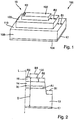
- FIG. 1 schematically shows a perspective view of a first embodiment of a stacked III-V semiconductor device 10 according to the invention.
- the semiconductor device 10 has a stack 100 comprising a plurality of semiconductor layers, with a rectangular upper side 102, a rectangular lower side 104 and a side surface 106 connecting the upper side 102 and the lower side 104.
- the lower side 104 is larger than the upper side 102.
- the side surface 106 consists of four Stair-shaped surfaces, so that form in the region of the side surface 106, a first circumferential paragraph-shaped edge 110 with a first width 120 B1 and a second circumferential paragraph-shaped edge with a second width B2.
- the underside 104 of the stack 100 is completely covered by a first contact layer K1.
- a second contact layer K2 is arranged on the upper side 102 of the semiconductor component 10.
- a first embodiment of the layer sequence of the semiconductor layers of the stack 100 of the semiconductor device 10 is shown in the figure FIG. 2 shown.
- the stack 100 has along a longitudinal axis L a layered p + region 12 with a dopant concentration of 5 ⁇ 10 18 -5 ⁇ 10 20 N / cm 3 , an n - layer with a dopant concentration of 10 12 -10 17 N / cm 3 and a layered n + region with a dopant concentration of at least 10 19 N / cm 3 , each layer having a bottom and a top.
- the p + layer 12 is formed as a substrate with a layer thickness D1, wherein the underside of the p + layer 12 forms the bottom of the stack 100.
- a first part of the top of the p + layer 12 forms the circumferential first edge 110 with the width B1.
- the underside of the n - layer 14 is arranged on a second part of the top of the p + layer 12.
- the n - layer 14 has a layer thickness D2.
- a part of the top of the n - layer forms the circumferential second edge 130 with a width B2.
- the underside of the n + -layer 16 is arranged on a second part of the upper side of the n - -layer 14.
- the n + -layer 16 has a layer thickness D3.
- the top of the n + layer 16 forms the top of the stack 100.
- the underside of the stack 100 is completely covered by the first contact layer K1.
- the second contact layer K2 is formed flat on a central region of the upper side of the stack 100, so that the upper side of the stack 100, in this case the n + -layer 16, forms a third peripheral, stepped edge 130 with a width B3.
- All layers 12, 14 and 16 are monolithic and comprise a GaAs compound or consist of a GaAs compound.
- the stack 100 has a defect layer 30 with a layer thickness D4, wherein the defect layer is arranged within the n - layer 14 and to the underside of the n - layer 14 or the top of the p + layer 12 has a distance A1.
- FIG. 3 In the picture of the FIG. 3 a further embodiment of a layer sequence according to the invention of the III-V semiconductor device is shown. The following are just the differences from the illustration of FIG. 2 explained.
- n + layer 16 is formed as a substrate layer, followed by the n - layer 14, a p- or n-doped intermediate layer 18 with a layer thickness D5 and the p + layer 12.
- an area of the stack 100 adjacent to the side surface is made insulating from the first circumferential edge 110 to an edge adjacent to the top side of the stack 100 and forms a first insulation layer 20.
- a second insulating layer 22, e.g. an oxide layer or a combination of an oxide layer and a nitride layer is deposited by chemical vapor deposition on the side surfaces in the region from the first circumferential edge 110 to an edge adjacent to the top of the stack 100.
- the insulating layer 22 may extend to the surface 102
Landscapes
- Engineering & Computer Science (AREA)
- Microelectronics & Electronic Packaging (AREA)
- Power Engineering (AREA)
- Physics & Mathematics (AREA)
- Ceramic Engineering (AREA)
- Condensed Matter Physics & Semiconductors (AREA)
- General Physics & Mathematics (AREA)
- Computer Hardware Design (AREA)
- Manufacturing & Machinery (AREA)
- Electrodes Of Semiconductors (AREA)
- Recrystallisation Techniques (AREA)
Abstract
Stapelförmiges III-V-Halbleiterbauelement (10) aufweisen einen Stapel (100) mit einer Oberseite (102), einer Unterseite (104), einer Seitenfläche (106) und einer Längsachse (L), wobei der Stapel (100) einen p+-Bereich (12), eine n--Schicht (14) und einen n+-Bereich (16) aufweist, der p+-Bereiche (12), die n--Schicht (14) und der n+-Bereich (16) entlang der Längsachse (L) in der genannten Reihenfolge aufeinander folgen, monolithisch ausgebildet sind und eine GaAs-Verbindung umfassen, der n+-Bereich (16) oder der p+-Bereich (12) als Substratschicht ausgebildet ist, der Stapel (100) im Bereich der Seitenfläche (106) einen ersten und einen zweiten umlaufenden absatzförmigen Rand (110, 120) aufweist, der erste Rand (110) von der Substratschicht gebildet wird, der zweite Rand (120) von der n--Schicht (16) oder von einer an die n--Schicht (16) und den p+-Bereich (12) angrenzenden Zwischenschicht (18) gebildet wird und der erste und der zweite umlaufende Rand (110, 120) jeweils eine Breite von mindestens 10 µm aufweisen.

Description
Die Erfindung betrifft ein stapelförmiges III-V-Halbleiterbauelement.The invention relates to a stacked III-V semiconductor device.
Aus
Aus "
Vor diesem Hintergrund besteht die Aufgabe der Erfindung darin, eine Vorrichtung anzugeben, die den Stand der Technik weiterbildet.Against this background, the object of the invention is to provide a device which further develops the prior art.
Die Aufgabe wird durch ein stapeiförmiges III-V-Haibleiterbauelement mit den Merkmalen des Patentanspruchs 1 gelöst. Vorteilhafte Ausgestaltungen der Erfindung sind Gegenstand von Unteransprüchen.The object is achieved by a stapeiförmiges III-V Haibleiterbauelement with the features of claim 1. Advantageous embodiments of the invention are the subject of dependent claims.
Gegenstand der Erfindung ist ein stapelförmiges III-V-Halbleiterbauelement, aufweisend einen Stapel mit einer Oberseite, einer Unterseite, einer die Oberseite und die Unterseite verbindenden Seitenfläche und einer durch die Oberseite und die Unterseite verlaufenden Längsachse.The invention relates to a stacked III-V semiconductor device, comprising a stack having an upper side, a lower side, a side surface connecting the upper side and the lower side, and a longitudinal axis extending through the upper side and the lower side.
Der Stapel weist einen p+-Bereich mit einer Oberseite, einer Unterseite und einer Dotierstoffkonzentration von 5•1018-5•1020 N/cm3, eine n--Schicht mit einer Oberseite und einer Unterseite, einer Dotierstoffkonzentration von 1012-1017 N/cm3 und einer Schichtdicke von 10 - 300 µm sowie einen n+-Bereich mit einer Oberseite, einer Unterseite und einer Dotierstoffkonzentration von mindestens 1019 N/cm3 auf.The stack has a p + region with a top, a bottom and a dopant concentration of 5 • 10 18 -5 • 10 20 N / cm 3 , an n - layer with a top and a bottom, a dopant concentration of 10 12 - 10 17 N / cm 3 and a layer thickness of 10 - 300 microns and an n + region with a top side, a bottom side and a dopant concentration of at least 10 19 N / cm 3 .
Der p+-Bereiche, die n--Schicht und der n+-Bereich folgen entlang der Längsachse des Stapels in der genannten Reihenfolge aufeinander, sind jeweils monolithisch ausgebildet und umfassen jeweils eine GaAs-Verbindung oder bestehen jeweils aus einer GaAs-Verbindung. Der n+-Bereich oder der p+-Bereich ist als Substratschicht ausgebildet.The p + region, the n - layer, and the n + region follow each other along the longitudinal axis of the stack in the order named, each formed monolithically and each comprise a GaAs compound or each consist of a GaAs compound. The n + region or the p + region is formed as a substrate layer.
Der Stapel weist im Bereich der Seitenfläche einen ersten umlaufenden, absatzförmigen Rand und einen zweiten umlaufenden absatzförmigen Rand auf, wobei der erste Rand von der Substratschicht gebildet wird, der zweite Rand von der n--Schicht oder von einer an die n--Schicht und den p+-Bereich angrenzenden Zwischenschicht gebildet wird und der erste umlaufende Rand und der zweite umlaufende Rand jeweils eine Breite von mindestens 10 µm aufweisen.The stack has, in the region of the side surface, a first peripheral, heel-shaped edge and a second circumferential heel-shaped edge, wherein the first edge is formed by the substrate layer, the second edge by the n - layer or one to the n - layer and The p + region adjacent intermediate layer is formed and the first peripheral edge and the second peripheral edge each have a width of at least 10 microns.
Die Oberseite und Unterseite des Stapels sind beispielsweise rechteckig, quadratisch oder rund ausgebildet. Als Seitenfläche werden alle die Unterseite mit der Oberseite verbindenden Flächenabschnitte bezeichnet, die den Stapel seitlich umschließen. Durch die absatzförmigen Ränder ist die Seitenfläche stufenförmig ausgebildet.The top and bottom of the stack are rectangular, square or round, for example. As a side surface all the underside connecting to the top surface sections are referred to, which surround the stack side. Due to the heel-shaped edges, the side surface is step-shaped.
Es sei angemerkt, dass die Schichten bevorzugt mittels einer Flüssigphasenepitaxie oder mittels einer MOVPE Anlage hergestellt werden.It should be noted that the layers are preferably produced by means of liquid phase epitaxy or by means of an MOVPE system.
Es versteht sich, dass das das Halbleiterbauelement mindestens zwei bevorzugt als Schichten ausgebildete Anschlusskontakte aufweist, wobei die Anschlusskontakte jeweils elektrisch leitfähig sind und metallische Eigenschaften aufweisen.It is understood that this has the semiconductor component at least two preferably formed as layers terminal contacts, wherein the terminal contacts are each electrically conductive and have metallic properties.
Bevorzugt bestehen die Anschlusskontaktschichten aus metallisch leitfähigen Halbleiterschichten oder Metallschichten oder einer Kombination aus beiden. Die Anschlusskontakte stellen einen elektrisch niederohmigen Kontakt zu den unmittelbar angrenzenden dotierten Halbleiterschichten her. Des Weiteren versteht es sich, dass die Anschlusskontakte vorzugsweise mittels Bonddrähte mit Kontaktfinger, den sogenannten Pins, verschaltet sind.The connection contact layers preferably consist of metallically conductive semiconductor layers or metal layers or a combination of both. The connection contacts provide an electrically low-resistance contact with the directly adjacent doped semiconductor layers ago. Furthermore, it is understood that the connection contacts are preferably connected by means of bonding wires with contact fingers, the so-called pins.
Die Anschlusskontakte sind bevorzugt auf einer Oberseite bzw. einer Unterseite des aus den Halbleiterbereichen bzw. Halbleiterschichten gebildeten Stapels angeordnet.The connection contacts are preferably arranged on an upper side or a lower side of the stack formed from the semiconductor regions or semiconductor layers.
Die umlaufenden absatzförmigen Ränder sind jeweils mittels eines Ätzprozesses hergestellt. Die Tiefe der Stufen, also der Abstand zwischen der Oberseite des Stapels und dem ersten Rand bzw. zwischen dem ersten Rand und dem zweiten Rand, wird bevorzugt über eine jeweilige Ätzzeit in Abhängigkeit von der Ätzrate kontrolliert.The circumferential heel-shaped edges are each produced by means of an etching process. The depth of the steps, that is to say the distance between the top side of the stack and the first edge or between the first edge and the second edge, is preferably controlled over a respective etching time as a function of the etching rate.
Ein Vorteil ist, dass sich mit der Strukturierung des Randes sich die Bauelementeigenschaften verbessern lassen. Insbesondere lassen sich die Sperrspannungen erhöhen und die Leckströme an der Oberfläche unterdrücken.One advantage is that the structuring of the edge improves the device properties. In particular, the blocking voltages can be increased and suppress the leakage currents at the surface.
Anders ausgedrückt lassen sich mit der erfindungsgemäßen III-V-Halbleiterdiode auf einfache Weise niedrige Leckströme bei Sperrspannungen in einem Bereich von 200V - 3000 V mit kleineren Einschaltwiderständen und geringeren Kapazitäten pro Fläche als herkömmliche hochsperrende Dioden aus Si oder aus SiC herstellen.In other words, with the III-V semiconductor diode of the present invention, low leakage currents at reverse voltages in a range of 200V-3000V with smaller on-resistances and lower capacitance per area can be easily produced than conventional Si high-blocking diodes or SiC.
Hierdurch sind Schaltfrequenzen von 30 kHz bis zu 0,5 GHz und Stromdichten von 0,5 A/mm2 bis 5 A/mm2 erreichbar.As a result, switching frequencies of 30 kHz to 0.5 GHz and current densities of 0.5 A / mm 2 to 5 A / mm 2 can be achieved.
Ein anderer Vorteil ist, dass sich die III-V-Halbleiterdioden kostengünstiger als vergleichbare hochsperrende Dioden aus SiC herstellen lassen.Another advantage is that the III-V semiconductor diodes can be produced more cost-effectively than comparable high-blocking diodes made of SiC.
Insbesondere lassen sich die erfindungsgemäßen III-V-Halbleiterdioden als Freilaufdioden verwenden.In particular, the III-V semiconductor diodes according to the invention can be used as freewheeling diodes.
Es sei angemerkt, dass die erfindungsgemäßen III-V-Halbleiterdioden vorliegend kleine Einschaltwiderstände in einem Bereich zwischen 1 mOhm und 200 mOhm aufweisen. Die Kapazitäten pro Fläche liegen in einem Bereich zwischen 2 pF und 100 pF.It should be noted that the III-V semiconductor diodes according to the invention in the present case have small turn-on resistances in a range between 1 mOhm and 200 mOhm. The capacities per area are in a range between 2 pF and 100 pF.
Ein anderer Vorteil der erfindungsgemäßen III-V-Halbleiterdiode ist eine hohe Temperaturfestigkeit von bis zu 300°C. Anders ausgedrückt lassen sich die III-V-Halbleiterdioden auch in heißen Umgebungen einsetzten. Hierbei sind niedrige Leckströme aufgrund des exponentiellen Anstiegs mit steigender Temperatur besonders hilfreich.Another advantage of the III-V semiconductor diode according to the invention is a high temperature resistance of up to 300 ° C. In other words, the III-V semiconductor diodes can also be used in hot environments. In this case, low leakage currents due to the exponential increase with increasing temperature are particularly helpful.
In einer Weiterbildung ist zumindest entlang eines Teils der Seitenflächen des Stapels in dem Stapel eine durch Implantation erzeugte erste Isolationsschicht ausgebildet. Die Isolationsschicht ist beispielsweise als amorphisierter Randbereich ausgebildet, wobei die Amorphisierung beispielsweise durch Implantation von Wasserstoff-Ionen erreicht wird.In a development, at least along a part of the side surfaces of the stack in the stack, a first insulation layer produced by implantation is formed. The insulation layer is formed for example as an amorphized edge region, wherein the amorphization is achieved for example by implantation of hydrogen ions.
Gemäß einer weiteren Weiterbildung erstreckt sich zumindest entlang eines Teils der Seitenfläche des Stapels eine Isolationsschicht. Beispielsweise wird mittels chemischer Gasphasenabscheidung (chemical vapor desposition, CVD) eine Oxidschicht auf die Seitenfläche aufgebracht. Die Oxidschicht weist bevorzugt eine Dicke von 10 µm -15 µm oder von 20 µm - 30 µm auf.According to a further development, an insulation layer extends at least along a part of the side surface of the stack. For example, an oxide layer is applied to the side surface by means of chemical vapor deposition (CVD). The oxide layer preferably has a thickness of 10 μm -15 μm or of 20 μm-30 μm.
In einer anderen Ausführungsform umfasst das Halbleiterbauelement eine erste Kontaktschicht und eine zweite Kontaktschicht, wobei die zweite Kontaktschicht die Oberseite des Stapels teilweise überdeckt, so dass die Oberseite des Stapels einen dritten umlaufenden Rand mit einer Breite von mindestens 10 µm um die zweite Kontaktschicht herum ausbildet. Die erste Kontaktschlcht überdeckt die Unterseite des Stapels bevorzugt vollständig.In another embodiment, the semiconductor device comprises a first contact layer and a second contact layer, the second contact layer partially covering the top of the stack so that the top of the stack forms a third circumferential edge of at least 10 μm width around the second contact layer. The first contact layer preferably completely covers the underside of the stack.
Gemäß einer anderen Ausführungsform sind der p+-Bereich und der n+-Bereich schichtförmig ausgebildet, wobei der schichtförmige n+-Bereich und der schichtförmige p+-Bereich jeweils stoffschlüssig mit der n--Schicht verbunden sind, der schichtförmige n+-Bereich eine Schichtdicke von 50 - 675 µm aufweist, der schichtförmige p+-Bereich eine Schichtdicke größer 2 µm aufweist, das stapelförmige III-V-Halbleiterbauelement eine erste Defektschicht mit einer Schichtdicke zwischen 0,5 µm und 50 µm aufweist und die Defektschicht innerhalb der n--Schicht angeordnet ist und eine Defektkonzentration in einem Bereich zwischen 1•1013 N/cm3 und 5•1016 N/cm3 aufweist.According to another embodiment, the p + region and the n + region are layered, wherein the layered n + region and the layered p + region are each connected in a materially bonded manner to the n - layer, the layered n + region a layer thickness of 50-675 has the layered p + region has a layer thickness greater than 2 microns, the stacked III-V semiconductor device has a first defect layer with a layer thickness between 0.5 .mu.m and 50 .mu.m and the defect layer is disposed within the n - layer and has a defect concentration in a range between 1 • 10 13 N / cm 3 and 5 • 10 16 N / cm 3 .
Es versteht sich, dass sich die Defektschicht auf unterschiedliche Weise, beispielsweise durch Implantation oder mittels Einbau von Fremdatomen erzeugen lässt und innerhalb der Defektschicht eine Rekombination von Ladungsträger erreicht wird. Vorzugsweise werden die Defekte bzw. die Rekombinationszentren durch Einbau von Chrom erreicht.It is understood that the defect layer can be produced in different ways, for example by implantation or by incorporation of foreign atoms, and recombination of charge carriers is achieved within the defect layer. Preferably, the defects or the recombination centers are achieved by incorporation of chromium.
Gemäß einer Weiterbildung beträgt eine Schichtdicke der Defektsicht ein Abstand der Defektschicht zu einer Grenzfläche zwischen der n--Schicht und der p+-Bereich höchstens die Hälfte der Schichtdicke der n--Schicht.According to a development, a layer thickness of the defect view is a distance of the defect layer to an interface between the n - layer and the p + region at most half the layer thickness of the n - layer.
Es sei angemerkt, dass die Defektschicht vorzugsweise nicht innerhalb der Raumladungszone ausgebildet ist. Vorzugsweise ist die Dicke der n--Schicht derart ausgebildet, dass die Defektschicht von der Raumladungszone beabstandet ist.It should be noted that the defect layer is preferably not formed within the space charge region. Preferably, the thickness of the n - layer is formed such that the defect layer is spaced from the space charge zone.
In einer weiteren Ausführungsform sind der p+-Bereich und der n+-Bereich schichtförmig ausgebildet, wobei der schichtförmige n+-Bereich stoffschlüssig mit der n--Schicht verbunden ist, zwischen der n--Schicht und der p+-Schicht eine dotierte Zwischenschicht mit einer Schichtdicke von 1-50 µm und einer Dotierstoffkonzentration von 1012-1017 cm-3 angeordnet ist und die Zwischenschicht mit der n--Schicht und mit der p+-Schicht stoffschlüssig verbunden ist.In another embodiment, the p + -type region and the n + -type region are formed in layers, wherein the layer-shaped n + region cohesively with the n - layer is connected, between the n - layer and p + layer, a doped Intermediate layer with a layer thickness of 1-50 microns and a dopant concentration of 10 12 -10 17 cm -3 is arranged and the intermediate layer with the n - layer and with the p + layer is firmly bonded.
Es versteht sich, dass die Zwischenschicht eine im Vergleich zu den stoffschlüssig verbundenen Schichten wenigstens eine unterschiedliche Dotierstoffkonzentration aufweist.It is understood that the intermediate layer has at least one different dopant concentration compared to the cohesively connected layers.
Bevorzugt ist die Zwischenschicht p-dotiert und umfasst besonders bevorzugt Zink oder Kohlenstoff als Dotierstoffe. Die Dotierstoffkonzentration der p-dotierten Zwischenschicht ist besonders bevorzugt kleiner als die Dotierstoffkonzentration des p+-Bereichs, insbesondere um einen Faktor 2 bis zu einem Faktor von 5 Größenordnungen.The intermediate layer is preferably p-doped and particularly preferably comprises zinc or carbon as dopants. The dopant concentration of the p-doped intermediate layer is particularly preferably smaller than the dopant concentration of the p + region, in particular by a factor of 2 up to a factor of 5 orders of magnitude.
Alternativ ist die Zwischenschicht n-dotiert und umfasst bevorzugt Silizium und/oder Zinn, wobei die Dotierstoffkonzentration der n-dotierten Zwischenschicht besonders bevorzugt um bis zu einem Faktor 100 kleiner als die Dotierstoffkonzentration des n--Bereichs ist.Alternatively, the intermediate layer is n-doped and preferably comprises silicon and / or tin, wherein the dopant concentration of the n-doped intermediate layer is particularly preferably smaller by up to a factor of 100 than the dopant concentration of the n - region.
In einer Weiterbildung ist die III-V-Halbleiterdiode monolithisch ausgebildet, d.h. die einzelnen monolithisch ausgebildeten Schichten sind zueinander ebenfalls monolithisch ausgebildet.In a further development, the III-V semiconductor diode is monolithic, i. the individual monolithically formed layers are also monolithic to each other.
In einer anderen Ausführungsform umfasst die III-V Halbleiterdiode wenigstens einen Halbleiterbond.In another embodiment, the III-V semiconductor diode comprises at least one semiconductor bond.
Es wird angemerkt, dass der Ausdruck Halbleiterbond synonym mit dem Ausdruck Waferbond verwendet wird.It is noted that the term semiconductor bond is used synonymously with the term wafer-bond.
In einer weiteren Ausführungsform ist der Halbleiterbond bei dem stapelförmigen Schichtaufbau, bestehend aus dem p+-Schicht, der p-dotierten Zwischenschicht, der n--Schicht und der n+-Schicht, zwischen der n--Schicht und der p-dotierten Zwischenschicht ausgebildet.In a further embodiment, the semiconductor bond in the stacked layer structure consisting of the p + layer, the p-doped intermediate layer, the n - layer and the n + layer, between the n - layer and the p-doped intermediate layer educated.
In einer Ausführungsform bildet der Schichtaufbau bestehend aus einem p+-Schicht und der p-dotierten Zwischenschicht einen ersten Teilstapel und der Schichtaufbau bestehend aus der n+-Schicht und der n--Schicht einen zweiten Teilstapel.In one embodiment, the layer structure consisting of a p + layer and the p-doped intermediate layer forms a first partial stack and the layer structure consisting of the n + layer and the n - layer forms a second partial stack.
In einer Weiterbildung wird der erste Teilstapel gebildet, in dem ausgehend von einem p+-Schicht mittels Epitaxie die p-dotierten Zwischenschicht hergestellt wird.In a development, the first partial stack is formed in which, starting from a p + layer, the p-doped intermediate layer is produced by means of epitaxy.
Vorzugsweise weist die als p--Schicht ausgebildete Zwischenschicht eine Dotierung kleiner als 1013 N/cm3 oder eine Dotierung zwischen 1013 N/cm3 und 1015 N/cm3 auf. In einer Ausführungsform wird das p+-Schicht vor oder nach dem Bonden durch einen Schleifprozess auf eine Dicke zwischen 200 µm und 500 µm gedünnt.The intermediate layer formed as a p - layer preferably has a doping of less than 10 13 N / cm 3 or a doping of between 10 13 N / cm 3 and 10 15 N / cm 3 . In one embodiment, the p + layer is thinned before or after bonding by a grinding process to a thickness of between 200 μm and 500 μm.
In einer Weiterbildung sind der erste Teilstapel und der zweite Teilstapel jeweils monolithisch ausgebildet.In a development, the first partial stack and the second partial stack are each formed monolithically.
In einer Ausführungsform wird der zweite Stapel gebildet, in dem ausgehend von einem n--Substrat, das n--Substrat mit dem zweiten Stapel durch einen weiteren Waferbondprozess verbunden wird.In one embodiment, the second stack is formed in which, starting from an n - substrate, the n - substrate is connected to the second stack by a further wafer bonding process.
In einem weiteren Prozessschritt wird das n--Substrat auf die gewünschte Dicke gedünnt. Vorzugsweise liegt die Dicke des n--Substrats in einem Bereich zwischen 50 µm bis 250µm. Vorzugsweise liegt die Dotierung des n'-Substrats in einem Bereich zwischen 1013 N/cm3 und 1015 N/cm3.In a further process step, the n - substrate is thinned to the desired thickness. Preferably, the thickness of the n - substrate is in a range between 50 .mu.m to 250 .mu.m. Preferably, the doping of the n'-substrate is in a range between 10 13 N / cm 3 and 10 15 N / cm 3 .
Ein Vorteil des Waferbondens ist es, dass sich dicke n--Schichten ohne weiteres herstellen lassen. Ein langer Abscheideprozess bei der Epitaxie entfällt hierdurch. Auch lassen sich mittels des Bondens die Anzahl der Stapelfehler bei den dicken n--Schichten verringern.An advantage of wafer bondering is that thick n - layers can be readily prepared. This eliminates a long epitaxial deposition process. Also, by means of bonding, the number of stacking faults in the thick n - layers can be reduced.
In einer anderen Weiterbildung wird vor dem Bonden die Defektschicht vorzugsweise mittels Implantation von Ionen in die Oberfläche des ersten Teilstapels, d.h. in die p-dotierten Zwischenschicht erzeugt.In another embodiment, prior to bonding, the defect layer is preferably formed by implanting ions into the surface of the first sub-stack, i. generated in the p-doped intermediate layer.
In eine alternativen Ausführungsform weist das n--Substrat eine Dotierung größer als 1010 N/cm-3 und kleiner als 1013 N/cm-3 auf. In dem die Dotierung extrem gering ist, lässt sich das n--Substrat auch als eine intrinsische Schicht auffassen.In an alternative embodiment, the n - substrate has a doping greater than 10 10 N / cm -3 and less than 10 13 N / cm -3 . In that the doping is extremely low, the n - substrate can also be considered as an intrinsic layer.
In einer Weiterbildung wird nach dem Dünnen des n--Substrats mittels Epitaxie oder Hochdosisimplantation auf dem n--Substrat die n+-Schicht in einem Bereich zwischen 1018 N/cm3 und kleiner als 5x10¹⁹ N/cm3 erzeugt.Substrate by means of epitaxy or high-dose implantation in the n - - In a further development, after thinning the substrate generates n n + layer in a range between 10 18 N / cm 3 and less than 5x10 19 N / cm 3.
Es versteht sich, dass das Dünnen des n--Substrats vorzugsweise mittels eines CMP Schrittes, d.h. mittels chemischen mechanischen Polierens erfolgt.It is understood that the thinning of the n - substrate preferably takes place by means of a CMP step, ie by means of chemical mechanical polishing.
In einer anderen Weiterbildung wird auf der Vorderseite der Dioden-Struktur eine Hilfsschicht aufgetragen. Anschließend lässt die Rückseite der Dioden-Struktur dünnen und auf einem Träger ablegen. In einer anderen Weiterbildung wird anschließend die Hilfsschicht von der Vorderseite abgelöst.In another development, an auxiliary layer is applied to the front side of the diode structure. Subsequently, the back of the diode structure leaves thin and placed on a support. In another development, the auxiliary layer is then detached from the front side.
In einer Ausführungsform werden die Oberfläche des n+-Substrats und die Oberfläche der p+-Schicht metallisiert, um die Halbleiter-Diode elektrisch anzuschließen. Vorzugsweise wird die Kathode der Halbleiter-Diode nach der Metallisierung mit einer als Wärmesenke ausgebildeten Unterlage stoffschlüssig verbunden. Anders ausgedrückt, die Anode ist an der Oberfläche der Diode auf der p+-Schicht ausgebildet.In one embodiment, the surface of the n + substrate and the surface of the p + layer are metallized to electrically connect the semiconductor diode. Preferably, the cathode of the semiconductor diode after the metallization is materially connected to a trained as a heat sink pad. In other words, the anode is formed on the surface of the diode on the p + layer.
Untersuchungen haben gezeigt, dass sich mit bestimmten Kombinationen von einer p-- Zwischenschicht und n--Schicht verschiedene Sperrspannungen erzielen lassen.Investigations have shown that different blocking voltages can be achieved with certain combinations of a p - - interlayer and n - layer.
In einer ersten Variante umfasst die:
p-- Zwischenschicht eine Dicke zwischen 10 µm bis 25 µm und für die n--Schicht eine Dicke zwischen 40 µm und 90 µm eine Sperrspannung von ca. 900 V ergibt.In a first variant, the:
p - - intermediate layer has a thickness between 10 .mu.m to 25 .mu.m and for the n - layer a thickness between 40 .mu.m and 90 .mu.m gives a blocking voltage of about 900 V.
In einer zweiten Variante umfasst die:
p-- Zwischenschicht eine Dicke zwischen 25 µm bis 35 µm und für die n--Schicht eine Dicke zwischen 40 µm und 70 µm eine Sperrspannung von ca. 1200 V ergibt.In a second variant, the:
p - - intermediate layer has a thickness between 25 μm to 35 μm and for the n - layer a thickness between 40 μm and 70 μm results in a blocking voltage of about 1200 V.
In einer dritten Variante umfasst die:
p-- Zwischenschicht eine Dicke zwischen 35 µm bis 50 µm und für die n--Schicht eine Dicke zwischen 70µm und 150 µm und 70 µm eine Sperrspannung von ca. 1500 V ergibt.In a third variant, the:
p - - intermediate layer has a thickness between 35 microns to 50 microns and the n - layer results in a thickness of between 70 .mu.m and 150 .mu.m and 70 .mu.m a reverse voltage of about 1500 V.
Die Dioden in der ersten bis dritten Variante lassen sich auch als Punsch- Dioden bezeichnen.The diodes in the first to third variants can also be referred to as punch diodes.
In einer vierten Variante umfasst die:
p-- Zwischenschicht eine Dicke zwischen 10 µm bis 25 µm und für die n--Schicht eine Dicke zwischen 60 µm und 110 µm.In a fourth variant, the:
p - - intermediate layer has a thickness between 10 .mu.m to 25 .mu.m and for the n - layer has a thickness between 60 .mu.m and 110 .mu.m.
In einer fünften Variante umfasst die:
p-- Zwischenschicht eine Dicke zwischen 10 µm bis 25 µm und für die n--Schicht eine Dicke zwischen 70 µm und 140.In a fifth variant, it includes:
p - - intermediate layer has a thickness between 10 μm to 25 μm and for the n - layer a thickness between 70 μm and 140.
In einer sechsten Variante umfasst die:
p-- Zwischenschicht eine Dicke zwischen 35 µm bis 50 µm und für die n--Schicht eine Dicke zwischen 80µm und 200 µm.In a sixth variant, the:
p - - intermediate layer has a thickness between 35 μm to 50 μm and for the n - layer a thickness between 80 μm and 200 μm.
Die Dioden in der vierten bis sechsten Variante lassen sich auch als "non - reach - through" - Dioden bezeichnen.The diodes in the fourth to sixth variants can also be referred to as "non - reach - through" diodes.
Die Erfindung wird nachfolgend unter Bezugnahme auf die Zeichnungen näher erläutert. Hierbei werden gleichartige Teile mit identischen Bezeichnungen beschriftet. Die dargestellten Ausführungsformen sind stark schematisiert, d.h. die Abstände und die lateralen und die vertikalen Erstreckungen sind nicht maßstäblich und weisen, sofern nicht anders angegeben, auch keine ableitbaren geometrischen Relationen zueinander auf. Darin zeigt:
- Figur 1
- eine schematische Ansicht auf eine erste erfindungsgemäße Ausführungsform eines Halbleiterbauelements,
- Figur 2
- eine schematische Schnittansicht der Schichtenfolge einer erfindungsgemäße Ausführungsform eines Halbleiterbauelements,
- Figur 3
- eine schematisch Schnittansicht der Schichtfolgen einer zweiten erfindungsgemäßen Ausführungsform eines Halbleiterbauelements.
- FIG. 1
- a schematic view of a first embodiment of a semiconductor device according to the invention,
- FIG. 2
- a schematic sectional view of the layer sequence of an embodiment of a semiconductor device according to the invention,
- FIG. 3
- a schematic sectional view of the layer sequences of a second embodiment of a semiconductor device according to the invention.
Die Abbildung der
Das Halbleiterbauelement 10 weist einen aus mehreren Halbleiterschichten bestehenden Stapel 100 mit einer rechteckigen Oberseite 102, einer rechteckigen Unterseite 104 und einer die Oberseite 102 und die Unterseite 104 verbindenden Seitenfläche 106. Die Unterseite 104 ist größer als die Oberseite 102. Die Seitenfläche 106 besteht aus vier Treppenförmigen Flächen, so dass sich im Bereich der Seitenfläche 106 ein erster umlaufender absatzförmiger Rand 110 mit einer ersten Breite 120 B1 und ein zweiter umlaufender absatzförmiger Rand mit einer zweiten Breite B2 ausbilden.The
Die Unterseite 104 des Stapels 100 ist vollständig von einer ersten Kontaktschicht K1 bedeckt. Eine zweite Kontaktschicht K2 ist auf der Oberseite 102 des Halbleiterbauelements 10 angeordnet.The
Eine erste Ausführungsform der Schichtenfolge der Halbleiterschichten des Stapels 100 des Halbleiterbauelements 10 ist in der Abbildung der
Der Stapel 100 weist entlang einer Längsachse L einen schichtförmigen p+-Bereich 12 mit einer Dotierstoffkonzentration von 5•1018-5•1020 N/cm3, eine n--Schicht mit einer Dotierstoffkonzentration von 1012-1017 N/cm3 und einen schichtförmigen n+-Bereich mit einer Dotierstoffkonzentration von mindestens 1019 N/cm3 auf, wobei jede Schicht eine Unterseite und eine Oberseite aufweist.The
Die p+-Schicht 12 ist als Substrat mit einer Schichtdicke D1 ausgebildet, wobei die Unterseite der p+-Schicht 12 die Unterseite des Stapels 100 ausbildet. Ein erster Teil der Oberseite der p+-Schicht 12 bildet den umlaufenden ersten Rand 110 mit der Breite B1 aus. Auf einem zweiten Teil der Oberseite der p+-Schicht 12 ist die Unterseite der n--Schicht 14 angeordnet. Die n--Schicht 14 weist eine Schichtdicke D2 auf. Ein Teil der Oberseite der n--Schicht bildet den umlaufenden zweiten Rand 130 mit einer Breite B2 aus. Auf einem zweiten Teil der Oberseite der n--Schicht 14 ist die Unterseite der n+-Schicht 16 angeordnet. Die n+-Schicht 16 weist eine Schichtdicke D3 auf. Die Oberseite der n+-Schicht 16 bildet die Oberseite des Stapels 100 aus.The p + layer 12 is formed as a substrate with a layer thickness D1, wherein the underside of the p + layer 12 forms the bottom of the
Die Unterseite des Stapels 100 ist vollständig von der ersten Kontaktschicht K1 bedeckt. Die zweite Kontaktschicht K2 ist flächig auf einem zentralen Bereich der Oberseite des Stapels 100 ausgebildet, so dass die Oberseite des Stapels 100, also hier die n+-Schicht 16, einen dritten umlaufenden, absatzförmigen Rand 130 mit einer Breite B3 ausbildet.The underside of the
Alle Schichten 12, 14 und 16 sind monolithisch ausgebildet und umfassen eine GaAs-Verbindung oder bestehen aus einer GaAs-Verbindung.
Optional und daher gestrichelt eingezeichnet, weist der Stapel 100 eine Defektschicht 30 mit einer Schichtdicke D4 auf, wobei die Defektschicht innerhalb der n--Schicht 14 angeordnet ist und zu der Unterseite der n--Schicht 14 bzw. der Oberseite der p+-Schicht 12 einen Abstand A1 aufweist.All layers 12, 14 and 16 are monolithic and comprise a GaAs compound or consist of a GaAs compound.
Optionally and therefore shown in dashed lines, the
In der Abbildung der
Die n+-Schicht 16 ist als Substratschicht ausgebildet, gefolgt von der n--Schicht 14, einer p- oder n-dotierten Zwischenschicht 18 mit einer Schichtdicke D5 und der p+-Schicht 12.The n + layer 16 is formed as a substrate layer, followed by the n - layer 14, a p- or n-doped intermediate layer 18 with a layer thickness D5 and the p + layer 12.
Durch Implantation ist ein an die Seitenfläche angrenzender Bereich des Stapels 100 von dem ersten umlaufenden Rand 110 bis zu einem an die Oberseite des Stapels 100 angrenzenden Kante isolierend ausgebildet und bildet eine erste Isolationsschicht 20 aus.By implantation, an area of the
Eine zweite Isolationsschicht 22, z.B. eine Oxidschicht oder eine Kombination aus einer Oxidschicht und einer Nitridschicht, ist mittels chemischer Gasphasenabscheidung auf die Seitenflächen im Bereich von dem ersten umlaufenden Rand 110 bis zu einer an die Oberseite des Stapels 100 angrenzenden Kante aufgebracht. Dabei kann sich die Isolationsschicht 22 bis zur Oberfläche 102 erstreckenA second insulating
Claims (9)
dadurch gekennzeichnet, dass
characterized in that
Applications Claiming Priority (1)
| Application Number | Priority Date | Filing Date | Title |
|---|---|---|---|
| DE102018002895.0A DE102018002895A1 (en) | 2018-04-09 | 2018-04-09 | Stacked III-V semiconductor device |
Publications (2)
| Publication Number | Publication Date |
|---|---|
| EP3553827A1 true EP3553827A1 (en) | 2019-10-16 |
| EP3553827B1 EP3553827B1 (en) | 2020-07-22 |
Family
ID=66101786
Family Applications (1)
| Application Number | Title | Priority Date | Filing Date |
|---|---|---|---|
| EP19000163.6A Active EP3553827B1 (en) | 2018-04-09 | 2019-04-01 | Stacked iii-v semi-conductor device |
Country Status (5)
| Country | Link |
|---|---|
| US (1) | US10784381B2 (en) |
| EP (1) | EP3553827B1 (en) |
| JP (1) | JP6885619B2 (en) |
| CN (1) | CN110364565B (en) |
| DE (1) | DE102018002895A1 (en) |
Cited By (2)
| Publication number | Priority date | Publication date | Assignee | Title |
|---|---|---|---|---|
| EP3882980A3 (en) * | 2020-03-20 | 2021-09-29 | AZUR SPACE Solar Power GmbH | Stacked blocking iii-v power semiconductor diode |
| EP3886179A1 (en) * | 2020-03-20 | 2021-09-29 | AZUR SPACE Solar Power GmbH | Stacked high-barrier ingaas semiconductor power diode |
Families Citing this family (1)
| Publication number | Priority date | Publication date | Assignee | Title |
|---|---|---|---|---|
| DE102021001116A1 (en) * | 2021-03-02 | 2022-09-08 | Azur Space Solar Power Gmbh | Method of plating |
Citations (3)
| Publication number | Priority date | Publication date | Assignee | Title |
|---|---|---|---|---|
| US5213994A (en) * | 1989-05-30 | 1993-05-25 | Motorola, Inc. | Method of making high voltage semiconductor device |
| US20060281263A1 (en) * | 2005-05-20 | 2006-12-14 | Shinya Yamazaki | Semiconductor devices and method of manufacturing them |
| US20170069714A1 (en) * | 2015-09-04 | 2017-03-09 | Kabushiki Kaisha Toshiba | Semiconductor device and method of manufacturing the same |
Family Cites Families (13)
| Publication number | Priority date | Publication date | Assignee | Title |
|---|---|---|---|---|
| JPS4915908B1 (en) | 1969-09-02 | 1974-04-18 | ||
| JP2851044B2 (en) * | 1988-03-30 | 1999-01-27 | 株式会社東芝 | Method for manufacturing semiconductor device |
| IL101966A (en) * | 1992-05-22 | 1998-04-05 | Ramot Ramatsity Authority For | PROCESS FOR FABRICATING Gallium Arsenide p-i-n STRUCTURE |
| US6054369A (en) * | 1997-06-30 | 2000-04-25 | Intersil Corporation | Lifetime control for semiconductor devices |
| JPH11307806A (en) * | 1998-04-17 | 1999-11-05 | Matsushita Electric Ind Co Ltd | Photodetector and its manufacture |
| US20070228505A1 (en) * | 2006-04-04 | 2007-10-04 | Mazzola Michael S | Junction barrier schottky rectifiers having epitaxially grown p+-n junctions and methods of making |
| WO2008019377A2 (en) * | 2006-08-07 | 2008-02-14 | Semi-Photonics Co., Ltd. | Method of separating semiconductor dies |
| US20100213513A1 (en) | 2009-02-26 | 2010-08-26 | Skyworks Solutions, Inc. | Hyperabrupt Diode Structure And Method For Making Same |
| CN103700712B (en) * | 2012-09-27 | 2017-05-03 | 比亚迪股份有限公司 | Structure of fast recovery diode (FRD) and manufacturing method thereof |
| CN104952909A (en) | 2014-09-03 | 2015-09-30 | 安徽省祁门县黄山电器有限责任公司 | Junction terminal structure of diode chip |
| DE102015208097B4 (en) * | 2015-04-30 | 2022-03-31 | Infineon Technologies Ag | Manufacturing a semiconductor device by epitaxy |
| DE102015007326B3 (en) * | 2015-06-12 | 2016-07-21 | Azur Space Solar Power Gmbh | optocoupler |
| JP6611532B2 (en) | 2015-09-17 | 2019-11-27 | ローム株式会社 | Semiconductor device and manufacturing method of semiconductor device |
-
2018
- 2018-04-09 DE DE102018002895.0A patent/DE102018002895A1/en not_active Withdrawn
-
2019
- 2019-04-01 EP EP19000163.6A patent/EP3553827B1/en active Active
- 2019-04-08 JP JP2019073590A patent/JP6885619B2/en active Active
- 2019-04-09 US US16/379,008 patent/US10784381B2/en active Active
- 2019-04-09 CN CN201910279531.1A patent/CN110364565B/en active Active
Patent Citations (3)
| Publication number | Priority date | Publication date | Assignee | Title |
|---|---|---|---|---|
| US5213994A (en) * | 1989-05-30 | 1993-05-25 | Motorola, Inc. | Method of making high voltage semiconductor device |
| US20060281263A1 (en) * | 2005-05-20 | 2006-12-14 | Shinya Yamazaki | Semiconductor devices and method of manufacturing them |
| US20170069714A1 (en) * | 2015-09-04 | 2017-03-09 | Kabushiki Kaisha Toshiba | Semiconductor device and method of manufacturing the same |
Non-Patent Citations (2)
| Title |
|---|
| A. KOEL: "Characterization of the temperature dependent behavior of snappy phenomenon by the switching-off of GaAs power diode structures", ADVANCES IN FLUID MECHANICS XI, vol. 1, 1 July 2014 (2014-07-01), Southampton UK, pages 439 - 449, XP055545469, ISSN: 1746-4471, ISBN: 978-1-78466-105-2, DOI: 10.2495/HT140381 * |
| VIKTOR VOITOVICH ET AL: "LPE technology for power GaAs diode structures", ESTONIAN JOURNAL OF ENGINEERING, vol. 16, no. 1, 1 January 2010 (2010-01-01), pages 11 - 22, XP055498749, DOI: 10.3176/eng.2010.1.04 * |
Cited By (2)
| Publication number | Priority date | Publication date | Assignee | Title |
|---|---|---|---|---|
| EP3882980A3 (en) * | 2020-03-20 | 2021-09-29 | AZUR SPACE Solar Power GmbH | Stacked blocking iii-v power semiconductor diode |
| EP3886179A1 (en) * | 2020-03-20 | 2021-09-29 | AZUR SPACE Solar Power GmbH | Stacked high-barrier ingaas semiconductor power diode |
Also Published As
| Publication number | Publication date |
|---|---|
| US20190312151A1 (en) | 2019-10-10 |
| EP3553827B1 (en) | 2020-07-22 |
| CN110364565B (en) | 2022-11-01 |
| JP6885619B2 (en) | 2021-06-16 |
| US10784381B2 (en) | 2020-09-22 |
| CN110364565A (en) | 2019-10-22 |
| DE102018002895A1 (en) | 2019-10-10 |
| JP2019186549A (en) | 2019-10-24 |
Similar Documents
| Publication | Publication Date | Title |
|---|---|---|
| EP3514837B1 (en) | Iii-v semiconductor diode | |
| EP3557632B1 (en) | Gaas-based iii-v semiconductor diode | |
| EP3321970B1 (en) | Iii-v semiconductor diode | |
| EP3379577B1 (en) | Gaas-based iii-v semiconductor diode | |
| EP3522233B1 (en) | Stacked iii-v semiconductor diode | |
| DE102006056139B4 (en) | Semiconductor device with an improved structure for high withstand voltage | |
| DE112018003362T5 (en) | OXIDE SEMICONDUCTOR UNIT AND METHOD FOR PRODUCING AN OXID SEMICONDUCTOR UNIT | |
| EP3503204B1 (en) | Iii-v semi-conductor device | |
| EP3553827B1 (en) | Stacked iii-v semi-conductor device | |
| DE19701189A1 (en) | Semiconductor device | |
| DE102011080258A1 (en) | Super junction Schottky oxide PiN diode | |
| EP0760528A2 (en) | Semiconductor device on silicium base with a high blocking voltage edge termination | |
| EP3343636B1 (en) | Igbt semiconductor structure | |
| EP3321972B1 (en) | Stacked schottky diode | |
| WO2000016403A1 (en) | Semiconductor device and semiconductor structure with contact | |
| EP3734667B1 (en) | Stacked iii-v power semiconductor diode with high blocking voltage | |
| DE1805261A1 (en) | Temperature compensated reference diode and method of making the same | |
| DE102019003068A1 (en) | InGaAS stacked high-blocking semiconductor power diode | |
| EP3882980A2 (en) | Stacked blocking iii-v power semiconductor diode | |
| EP3882979A1 (en) | Stacked blocking iii-v power semiconductor diode | |
| DE102021205424A1 (en) | semiconductor device | |
| DE102023134083A1 (en) | semiconductor device | |
| DE102020001841A1 (en) | Stacked high-blocking III-V semiconductor power diode |
Legal Events
| Date | Code | Title | Description |
|---|---|---|---|
| PUAI | Public reference made under article 153(3) epc to a published international application that has entered the european phase |
Free format text: ORIGINAL CODE: 0009012 |
|
| STAA | Information on the status of an ep patent application or granted ep patent |
Free format text: STATUS: THE APPLICATION HAS BEEN PUBLISHED |
|
| STAA | Information on the status of an ep patent application or granted ep patent |
Free format text: STATUS: REQUEST FOR EXAMINATION WAS MADE |
|
| AK | Designated contracting states |
Kind code of ref document: A1 Designated state(s): AL AT BE BG CH CY CZ DE DK EE ES FI FR GB GR HR HU IE IS IT LI LT LU LV MC MK MT NL NO PL PT RO RS SE SI SK SM TR |
|
| AX | Request for extension of the european patent |
Extension state: BA ME |
|
| 17P | Request for examination filed |
Effective date: 20190923 |
|
| RBV | Designated contracting states (corrected) |
Designated state(s): AL AT BE BG CH CY CZ DE DK EE ES FI FR GB GR HR HU IE IS IT LI LT LU LV MC MK MT NL NO PL PT RO RS SE SI SK SM TR |
|
| GRAJ | Information related to disapproval of communication of intention to grant by the applicant or resumption of examination proceedings by the epo deleted |
Free format text: ORIGINAL CODE: EPIDOSDIGR1 |
|
| GRAP | Despatch of communication of intention to grant a patent |
Free format text: ORIGINAL CODE: EPIDOSNIGR1 |
|
| GRAP | Despatch of communication of intention to grant a patent |
Free format text: ORIGINAL CODE: EPIDOSNIGR1 |
|
| RIC1 | Information provided on ipc code assigned before grant |
Ipc: H01L 29/36 20060101ALN20200312BHEP Ipc: H01L 29/20 20060101ALI20200312BHEP Ipc: H01L 21/18 20060101ALN20200312BHEP Ipc: H01L 29/06 20060101ALI20200312BHEP Ipc: H01L 29/861 20060101AFI20200312BHEP Ipc: H01L 29/34 20060101ALI20200312BHEP Ipc: H01L 29/32 20060101ALI20200312BHEP Ipc: H01L 21/329 20060101ALI20200312BHEP |
|
| STAA | Information on the status of an ep patent application or granted ep patent |
Free format text: STATUS: GRANT OF PATENT IS INTENDED |
|
| INTG | Intention to grant announced |
Effective date: 20200416 |
|
| RIC1 | Information provided on ipc code assigned before grant |
Ipc: H01L 21/329 20060101ALI20200406BHEP Ipc: H01L 29/06 20060101ALI20200406BHEP Ipc: H01L 29/861 20060101AFI20200406BHEP Ipc: H01L 29/34 20060101ALI20200406BHEP Ipc: H01L 21/18 20060101ALN20200406BHEP Ipc: H01L 29/20 20060101ALI20200406BHEP Ipc: H01L 29/36 20060101ALN20200406BHEP Ipc: H01L 29/32 20060101ALI20200406BHEP |
|
| GRAS | Grant fee paid |
Free format text: ORIGINAL CODE: EPIDOSNIGR3 |
|
| GRAA | (expected) grant |
Free format text: ORIGINAL CODE: 0009210 |
|
| STAA | Information on the status of an ep patent application or granted ep patent |
Free format text: STATUS: THE PATENT HAS BEEN GRANTED |
|
| AK | Designated contracting states |
Kind code of ref document: B1 Designated state(s): AL AT BE BG CH CY CZ DE DK EE ES FI FR GB GR HR HU IE IS IT LI LT LU LV MC MK MT NL NO PL PT RO RS SE SI SK SM TR |
|
| REG | Reference to a national code |
Ref country code: GB Ref legal event code: FG4D Free format text: NOT ENGLISH |
|
| REG | Reference to a national code |
Ref country code: CH Ref legal event code: EP |
|
| REG | Reference to a national code |
Ref country code: DE Ref legal event code: R096 Ref document number: 502019000090 Country of ref document: DE |
|
| REG | Reference to a national code |
Ref country code: AT Ref legal event code: REF Ref document number: 1294221 Country of ref document: AT Kind code of ref document: T Effective date: 20200815 |
|
| REG | Reference to a national code |
Ref country code: IE Ref legal event code: FG4D Free format text: LANGUAGE OF EP DOCUMENT: GERMAN |
|
| REG | Reference to a national code |
Ref country code: CH Ref legal event code: NV Representative=s name: KIRKER AND CIE S.A., CH |
|
| REG | Reference to a national code |
Ref country code: LT Ref legal event code: MG4D |
|
| PG25 | Lapsed in a contracting state [announced via postgrant information from national office to epo] |
Ref country code: ES Free format text: LAPSE BECAUSE OF FAILURE TO SUBMIT A TRANSLATION OF THE DESCRIPTION OR TO PAY THE FEE WITHIN THE PRESCRIBED TIME-LIMIT Effective date: 20200722 Ref country code: BG Free format text: LAPSE BECAUSE OF FAILURE TO SUBMIT A TRANSLATION OF THE DESCRIPTION OR TO PAY THE FEE WITHIN THE PRESCRIBED TIME-LIMIT Effective date: 20201022 Ref country code: GR Free format text: LAPSE BECAUSE OF FAILURE TO SUBMIT A TRANSLATION OF THE DESCRIPTION OR TO PAY THE FEE WITHIN THE PRESCRIBED TIME-LIMIT Effective date: 20201023 Ref country code: NO Free format text: LAPSE BECAUSE OF FAILURE TO SUBMIT A TRANSLATION OF THE DESCRIPTION OR TO PAY THE FEE WITHIN THE PRESCRIBED TIME-LIMIT Effective date: 20201022 Ref country code: LT Free format text: LAPSE BECAUSE OF FAILURE TO SUBMIT A TRANSLATION OF THE DESCRIPTION OR TO PAY THE FEE WITHIN THE PRESCRIBED TIME-LIMIT Effective date: 20200722 Ref country code: FI Free format text: LAPSE BECAUSE OF FAILURE TO SUBMIT A TRANSLATION OF THE DESCRIPTION OR TO PAY THE FEE WITHIN THE PRESCRIBED TIME-LIMIT Effective date: 20200722 Ref country code: PT Free format text: LAPSE BECAUSE OF FAILURE TO SUBMIT A TRANSLATION OF THE DESCRIPTION OR TO PAY THE FEE WITHIN THE PRESCRIBED TIME-LIMIT Effective date: 20201123 Ref country code: SE Free format text: LAPSE BECAUSE OF FAILURE TO SUBMIT A TRANSLATION OF THE DESCRIPTION OR TO PAY THE FEE WITHIN THE PRESCRIBED TIME-LIMIT Effective date: 20200722 Ref country code: HR Free format text: LAPSE BECAUSE OF FAILURE TO SUBMIT A TRANSLATION OF THE DESCRIPTION OR TO PAY THE FEE WITHIN THE PRESCRIBED TIME-LIMIT Effective date: 20200722 |
|
| PG25 | Lapsed in a contracting state [announced via postgrant information from national office to epo] |
Ref country code: LV Free format text: LAPSE BECAUSE OF FAILURE TO SUBMIT A TRANSLATION OF THE DESCRIPTION OR TO PAY THE FEE WITHIN THE PRESCRIBED TIME-LIMIT Effective date: 20200722 Ref country code: PL Free format text: LAPSE BECAUSE OF FAILURE TO SUBMIT A TRANSLATION OF THE DESCRIPTION OR TO PAY THE FEE WITHIN THE PRESCRIBED TIME-LIMIT Effective date: 20200722 Ref country code: RS Free format text: LAPSE BECAUSE OF FAILURE TO SUBMIT A TRANSLATION OF THE DESCRIPTION OR TO PAY THE FEE WITHIN THE PRESCRIBED TIME-LIMIT Effective date: 20200722 Ref country code: IS Free format text: LAPSE BECAUSE OF FAILURE TO SUBMIT A TRANSLATION OF THE DESCRIPTION OR TO PAY THE FEE WITHIN THE PRESCRIBED TIME-LIMIT Effective date: 20201122 |
|
| PG25 | Lapsed in a contracting state [announced via postgrant information from national office to epo] |
Ref country code: NL Free format text: LAPSE BECAUSE OF FAILURE TO SUBMIT A TRANSLATION OF THE DESCRIPTION OR TO PAY THE FEE WITHIN THE PRESCRIBED TIME-LIMIT Effective date: 20200722 |
|
| REG | Reference to a national code |
Ref country code: DE Ref legal event code: R097 Ref document number: 502019000090 Country of ref document: DE |
|
| PG25 | Lapsed in a contracting state [announced via postgrant information from national office to epo] |
Ref country code: RO Free format text: LAPSE BECAUSE OF FAILURE TO SUBMIT A TRANSLATION OF THE DESCRIPTION OR TO PAY THE FEE WITHIN THE PRESCRIBED TIME-LIMIT Effective date: 20200722 Ref country code: DK Free format text: LAPSE BECAUSE OF FAILURE TO SUBMIT A TRANSLATION OF THE DESCRIPTION OR TO PAY THE FEE WITHIN THE PRESCRIBED TIME-LIMIT Effective date: 20200722 Ref country code: CZ Free format text: LAPSE BECAUSE OF FAILURE TO SUBMIT A TRANSLATION OF THE DESCRIPTION OR TO PAY THE FEE WITHIN THE PRESCRIBED TIME-LIMIT Effective date: 20200722 Ref country code: EE Free format text: LAPSE BECAUSE OF FAILURE TO SUBMIT A TRANSLATION OF THE DESCRIPTION OR TO PAY THE FEE WITHIN THE PRESCRIBED TIME-LIMIT Effective date: 20200722 Ref country code: SM Free format text: LAPSE BECAUSE OF FAILURE TO SUBMIT A TRANSLATION OF THE DESCRIPTION OR TO PAY THE FEE WITHIN THE PRESCRIBED TIME-LIMIT Effective date: 20200722 Ref country code: IT Free format text: LAPSE BECAUSE OF FAILURE TO SUBMIT A TRANSLATION OF THE DESCRIPTION OR TO PAY THE FEE WITHIN THE PRESCRIBED TIME-LIMIT Effective date: 20200722 |
|
| PLBE | No opposition filed within time limit |
Free format text: ORIGINAL CODE: 0009261 |
|
| STAA | Information on the status of an ep patent application or granted ep patent |
Free format text: STATUS: NO OPPOSITION FILED WITHIN TIME LIMIT |
|
| PG25 | Lapsed in a contracting state [announced via postgrant information from national office to epo] |
Ref country code: AL Free format text: LAPSE BECAUSE OF FAILURE TO SUBMIT A TRANSLATION OF THE DESCRIPTION OR TO PAY THE FEE WITHIN THE PRESCRIBED TIME-LIMIT Effective date: 20200722 |
|
| 26N | No opposition filed |
Effective date: 20210423 |
|
| PG25 | Lapsed in a contracting state [announced via postgrant information from national office to epo] |
Ref country code: SK Free format text: LAPSE BECAUSE OF FAILURE TO SUBMIT A TRANSLATION OF THE DESCRIPTION OR TO PAY THE FEE WITHIN THE PRESCRIBED TIME-LIMIT Effective date: 20200722 |
|
| PG25 | Lapsed in a contracting state [announced via postgrant information from national office to epo] |
Ref country code: SI Free format text: LAPSE BECAUSE OF FAILURE TO SUBMIT A TRANSLATION OF THE DESCRIPTION OR TO PAY THE FEE WITHIN THE PRESCRIBED TIME-LIMIT Effective date: 20200722 |
|
| REG | Reference to a national code |
Ref country code: NL Ref legal event code: MP Effective date: 20200722 |
|
| PG25 | Lapsed in a contracting state [announced via postgrant information from national office to epo] |
Ref country code: MC Free format text: LAPSE BECAUSE OF FAILURE TO SUBMIT A TRANSLATION OF THE DESCRIPTION OR TO PAY THE FEE WITHIN THE PRESCRIBED TIME-LIMIT Effective date: 20200722 |
|
| PG25 | Lapsed in a contracting state [announced via postgrant information from national office to epo] |
Ref country code: LU Free format text: LAPSE BECAUSE OF NON-PAYMENT OF DUE FEES Effective date: 20210401 |
|
| PG25 | Lapsed in a contracting state [announced via postgrant information from national office to epo] |
Ref country code: IE Free format text: LAPSE BECAUSE OF NON-PAYMENT OF DUE FEES Effective date: 20210401 |
|
| PG25 | Lapsed in a contracting state [announced via postgrant information from national office to epo] |
Ref country code: IS Free format text: LAPSE BECAUSE OF FAILURE TO SUBMIT A TRANSLATION OF THE DESCRIPTION OR TO PAY THE FEE WITHIN THE PRESCRIBED TIME-LIMIT Effective date: 20201122 |
|
| PG25 | Lapsed in a contracting state [announced via postgrant information from national office to epo] |
Ref country code: CY Free format text: LAPSE BECAUSE OF FAILURE TO SUBMIT A TRANSLATION OF THE DESCRIPTION OR TO PAY THE FEE WITHIN THE PRESCRIBED TIME-LIMIT Effective date: 20200722 |
|
| PG25 | Lapsed in a contracting state [announced via postgrant information from national office to epo] |
Ref country code: HU Free format text: LAPSE BECAUSE OF FAILURE TO SUBMIT A TRANSLATION OF THE DESCRIPTION OR TO PAY THE FEE WITHIN THE PRESCRIBED TIME-LIMIT; INVALID AB INITIO Effective date: 20190401 |
|
| PG25 | Lapsed in a contracting state [announced via postgrant information from national office to epo] |
Ref country code: MK Free format text: LAPSE BECAUSE OF FAILURE TO SUBMIT A TRANSLATION OF THE DESCRIPTION OR TO PAY THE FEE WITHIN THE PRESCRIBED TIME-LIMIT Effective date: 20200722 |
|
| PGFP | Annual fee paid to national office [announced via postgrant information from national office to epo] |
Ref country code: GB Payment date: 20240429 Year of fee payment: 6 |
|
| PGFP | Annual fee paid to national office [announced via postgrant information from national office to epo] |
Ref country code: DE Payment date: 20240320 Year of fee payment: 6 |
|
| PGFP | Annual fee paid to national office [announced via postgrant information from national office to epo] |
Ref country code: CH Payment date: 20240625 Year of fee payment: 6 |
|
| PGFP | Annual fee paid to national office [announced via postgrant information from national office to epo] |
Ref country code: FR Payment date: 20240429 Year of fee payment: 6 |
|
| PGFP | Annual fee paid to national office [announced via postgrant information from national office to epo] |
Ref country code: BE Payment date: 20240429 Year of fee payment: 6 |
|
| PG25 | Lapsed in a contracting state [announced via postgrant information from national office to epo] |
Ref country code: MT Free format text: LAPSE BECAUSE OF FAILURE TO SUBMIT A TRANSLATION OF THE DESCRIPTION OR TO PAY THE FEE WITHIN THE PRESCRIBED TIME-LIMIT Effective date: 20200722 |