EP3550296A1 - Halbleiterbauelement und potenzialmessvorrichtung - Google Patents
Halbleiterbauelement und potenzialmessvorrichtung Download PDFInfo
- Publication number
- EP3550296A1 EP3550296A1 EP17875259.8A EP17875259A EP3550296A1 EP 3550296 A1 EP3550296 A1 EP 3550296A1 EP 17875259 A EP17875259 A EP 17875259A EP 3550296 A1 EP3550296 A1 EP 3550296A1
- Authority
- EP
- European Patent Office
- Prior art keywords
- potential
- supply unit
- electrode
- amplifier
- supply
- Prior art date
- Legal status (The legal status is an assumption and is not a legal conclusion. Google has not performed a legal analysis and makes no representation as to the accuracy of the status listed.)
- Pending
Links
Images






Classifications
-
- G—PHYSICS
- G01—MEASURING; TESTING
- G01N—INVESTIGATING OR ANALYSING MATERIALS BY DETERMINING THEIR CHEMICAL OR PHYSICAL PROPERTIES
- G01N27/00—Investigating or analysing materials by the use of electric, electrochemical, or magnetic means
- G01N27/26—Investigating or analysing materials by the use of electric, electrochemical, or magnetic means by investigating electrochemical variables; by using electrolysis or electrophoresis
- G01N27/27—Association of two or more measuring systems or cells, each measuring a different parameter, where the measurement results may be either used independently, the systems or cells being physically associated, or combined to produce a value for a further parameter
-
- C—CHEMISTRY; METALLURGY
- C25—ELECTROLYTIC OR ELECTROPHORETIC PROCESSES; APPARATUS THEREFOR
- C25D—PROCESSES FOR THE ELECTROLYTIC OR ELECTROPHORETIC PRODUCTION OF COATINGS; ELECTROFORMING; APPARATUS THEREFOR
- C25D21/00—Processes for servicing or operating cells for electrolytic coating
- C25D21/12—Process control or regulation
-
- G—PHYSICS
- G01—MEASURING; TESTING
- G01N—INVESTIGATING OR ANALYSING MATERIALS BY DETERMINING THEIR CHEMICAL OR PHYSICAL PROPERTIES
- G01N27/00—Investigating or analysing materials by the use of electric, electrochemical, or magnetic means
- G01N27/26—Investigating or analysing materials by the use of electric, electrochemical, or magnetic means by investigating electrochemical variables; by using electrolysis or electrophoresis
- G01N27/28—Electrolytic cell components
- G01N27/30—Electrodes, e.g. test electrodes; Half-cells
-
- G—PHYSICS
- G01—MEASURING; TESTING
- G01N—INVESTIGATING OR ANALYSING MATERIALS BY DETERMINING THEIR CHEMICAL OR PHYSICAL PROPERTIES
- G01N27/00—Investigating or analysing materials by the use of electric, electrochemical, or magnetic means
- G01N27/26—Investigating or analysing materials by the use of electric, electrochemical, or magnetic means by investigating electrochemical variables; by using electrolysis or electrophoresis
- G01N27/28—Electrolytic cell components
- G01N27/30—Electrodes, e.g. test electrodes; Half-cells
- G01N27/301—Reference electrodes
-
- G—PHYSICS
- G01—MEASURING; TESTING
- G01N—INVESTIGATING OR ANALYSING MATERIALS BY DETERMINING THEIR CHEMICAL OR PHYSICAL PROPERTIES
- G01N27/00—Investigating or analysing materials by the use of electric, electrochemical, or magnetic means
- G01N27/26—Investigating or analysing materials by the use of electric, electrochemical, or magnetic means by investigating electrochemical variables; by using electrolysis or electrophoresis
- G01N27/416—Systems
-
- G—PHYSICS
- G01—MEASURING; TESTING
- G01N—INVESTIGATING OR ANALYSING MATERIALS BY DETERMINING THEIR CHEMICAL OR PHYSICAL PROPERTIES
- G01N33/00—Investigating or analysing materials by specific methods not covered by groups G01N1/00 - G01N31/00
- G01N33/48—Biological material, e.g. blood, urine; Haemocytometers
- G01N33/483—Physical analysis of biological material
- G01N33/487—Physical analysis of biological material of liquid biological material
- G01N33/48785—Electrical and electronic details of measuring devices for physical analysis of liquid biological material not specific to a particular test method, e.g. user interface or power supply
-
- G—PHYSICS
- G01—MEASURING; TESTING
- G01R—MEASURING ELECTRIC VARIABLES; MEASURING MAGNETIC VARIABLES
- G01R29/00—Arrangements for measuring or indicating electric quantities not covered by groups G01R19/00 - G01R27/00
- G01R29/12—Measuring electrostatic fields or voltage-potential
-
- H—ELECTRICITY
- H03—ELECTRONIC CIRCUITRY
- H03F—AMPLIFIERS
- H03F1/00—Details of amplifiers with only discharge tubes, only semiconductor devices or only unspecified devices as amplifying elements
- H03F1/52—Circuit arrangements for protecting such amplifiers
- H03F1/523—Circuit arrangements for protecting such amplifiers for amplifiers using field-effect devices
-
- H—ELECTRICITY
- H10—SEMICONDUCTOR DEVICES; ELECTRIC SOLID-STATE DEVICES NOT OTHERWISE PROVIDED FOR
- H10D—INORGANIC ELECTRIC SEMICONDUCTOR DEVICES
- H10D89/00—Aspects of integrated devices not covered by groups H10D84/00 - H10D88/00
- H10D89/60—Integrated devices comprising arrangements for electrical or thermal protection, e.g. protection circuits against electrostatic discharge [ESD]
- H10D89/601—Integrated devices comprising arrangements for electrical or thermal protection, e.g. protection circuits against electrostatic discharge [ESD] for devices having insulated gate electrodes, e.g. for IGFETs or IGBTs
- H10D89/611—Integrated devices comprising arrangements for electrical or thermal protection, e.g. protection circuits against electrostatic discharge [ESD] for devices having insulated gate electrodes, e.g. for IGFETs or IGBTs using diodes as protective elements
-
- G—PHYSICS
- G01—MEASURING; TESTING
- G01N—INVESTIGATING OR ANALYSING MATERIALS BY DETERMINING THEIR CHEMICAL OR PHYSICAL PROPERTIES
- G01N33/00—Investigating or analysing materials by specific methods not covered by groups G01N1/00 - G01N31/00
- G01N33/48—Biological material, e.g. blood, urine; Haemocytometers
- G01N33/483—Physical analysis of biological material
- G01N33/487—Physical analysis of biological material of liquid biological material
- G01N33/48707—Physical analysis of biological material of liquid biological material by electrical means
- G01N33/48735—Investigating suspensions of cells, e.g. measuring microbe concentration
-
- H—ELECTRICITY
- H03—ELECTRONIC CIRCUITRY
- H03F—AMPLIFIERS
- H03F2200/00—Indexing scheme relating to amplifiers
- H03F2200/444—Diode used as protection means in an amplifier, e.g. as a limiter or as a switch
Definitions
- the present disclosure relates to a semiconductor apparatus and a potential measuring apparatus, and more particularly, to a semiconductor apparatus and a potential measuring apparatus capable of preventing electrostatic breakdown during manufacturing.
- the present disclosure has been made in configuration of such circumstances, and particularly prevents deterioration in signal characteristics in potential measurement while providing a configuration for realizing plating processing in a potential measuring apparatus.
- a semiconductor apparatus includes a reference potential generating unit and a reference potential electrode that supply a reference potential to liquid filled into a container, a read electrode and an amplifier that read a signal from the liquid, a potential supply unit that fills plating solution instead of the liquid in the container and supplies a predetermined potential to the reference potential electrode and the read electrode when plating processing is performed on the reference potential electrode and the read electrode, and a breaker that blocks the supply of the predetermined potential from the potential supply unit at a position close to the amplifier at a time of potential measurement when the container is filled with the liquid, the reference potential generating unit supplies the reference potential to the liquid, the read electrode reads a signal from the liquid, and the signal read by the amplifier is amplified and output, and supplies the predetermined potential from the potential supply unit when the container is filled with the plating solution and the plating processing is performed, in which the reference potential generating unit, the reference potential electrode, the read electrode, the amplifier, the potential supply unit, and the breaker are installed on a same substrate.
- the breaker is a Field Effect Transistor (FET) switch and is controlled to be turned off at the time of the potential measurement to block the supply of the potential from the potential supply unit at a position close to the amplifier and is controlled to be turned on when the plating processing is performed so as to supply the predetermined potential from the potential supply unit.
- FET Field Effect Transistor
- the breaker can be a diode of which a cathode is connected to the potential supply unit and an anode is connected to the amplifier, and at the time of the potential measurement, it is possible that the potential supply unit supplies a first predetermined potential and blocks the supply of the potential from the potential supply unit at a position close to the amplifier, and when the plating processing is performed, it is possible that the potential supply unit supplies a second predetermined potential.
- the potential supply unit supplies a potential higher than the reference potential as a first predetermined potential and blocks the supply of the potential from the potential supply unit at a position close to the amplifier, and when the plating processing is performed, it is possible that the potential supply unit supplies a potential lower than a potential of the plating solution as a second predetermined potential.
- the potential supply unit can supply the predetermined potential from a power source of the amplifier.
- An additional diode can be further included that has the same characteristics as the diode and is formed by a same process as the diode, and of which a cathode is connected to the anode of the diode and an anode is connected to a ground potential.
- Another breaker can be included that blocks the supply of the predetermined potential from the potential supply unit at a position close to the reference potential generating unit at the time of the potential measurement and supplies the predetermined potential from the potential supply unit when the plating processing is performed.
- the another breaker is a Field Effect Transistor (FET) switch and is controlled to be turned off at the time of the potential measurement to block the supply of the potential from the potential supply unit at a position close to the reference potential generating unit and is controlled to be turned on when the plating processing is performed so as to supply the predetermined potential from the potential supply unit.
- FET Field Effect Transistor
- the another breaker can be another diode of which a cathode is connected to the potential supply unit and an anode is connected to the amplifier, and at the time of the potential measurement, it is possible that the potential supply unit supplies a first predetermined potential and blocks the supply of the potential from the potential supply unit at a position close to the amplifier, and when the plating processing is performed, it is possible that the potential supply unit supplies a second predetermined potential.
- the potential supply unit supplies a potential higher than the reference potential as a first predetermined potential and blocks the supply of the potential from the potential supply unit at a position close to the amplifier, and when the plating processing is performed, it is possible that the potential supply unit supplies a potential lower than a potential of the plating solution as a second predetermined potential.
- the potential supply unit can supply the predetermined potential from a power source of the amplifier.
- Another additional diode can be further included that has same characteristics as the another diode and is formed by a same process as the another diode, of which a cathode is connected to the anode of the another diode and an anode is connected to a ground potential.
- a potential measuring apparatus includes a reference potential generating unit and a reference potential electrode that supply a reference potential to liquid filled into a container, a read electrode and an amplifier that read a signal from the liquid, a potential supply unit that fills plating solution instead of the liquid in the container and supplies a predetermined potential to the reference potential electrode and the read electrode when plating processing is performed on the reference potential electrode and the read electrode, and a breaker that blocks the supply of the predetermined potential from the potential supply unit at a position close to the amplifier at a time of potential measurement when the container is filled with the liquid, the reference potential generating unit supplies the reference potential to the liquid, the read electrode reads a signal from the liquid, and the signal read by the amplifier is amplified and output, and supplies the predetermined potential from the potential supply unit when the container is filled with the plating solution and the plating processing is performed, in which the reference potential generating unit, the reference potential electrode, the read electrode, the amplifier, the potential supply unit, and the breaker are installed on a same substrate
- a reference potential generating unit and a reference potential electrode supply a reference potential to liquid filled in a container, a read electrode and an amplifier read a signal from the liquid, a potential supply unit fills plating solution instead of the liquid in the container, when plating processing is performed on the reference potential electrode and the read electrode, a predetermined potential is supplied to the reference potential electrode and the read electrode, the liquid is filled in the container, the reference potential generating unit supplies a reference potential to the liquid, at the time of potential measurement when the read electrode reads the signal from the liquid and the amplifier amplifies and outputs the read signal, a breaker blocks supply of the predetermined potential from the potential supply unit at a position close to the amplifier, and when the plating solution is filled in the container and the plating processing is performed, the predetermined potential from the potential supply unit is supplied, and the reference potential generating unit, the reference potential electrode, the read electrode, the amplifier, the potential supply unit, and the breaker are installed on a same substrate.
- FIG. 1 An upper part of Fig. 1 is a schematic perspective diagram of a potential measuring apparatus 1, a middle part of Fig. 1 is a wiring diagram corresponding to a top view of a petri dish 11 and an electrode substrate 12, and a lower part of Fig. 1 is a wiring diagram of a side cross section of the potential measuring unit 1.
- the potential measuring apparatus 1 includes the petri dish 11, the electrode substrate 12, and an Analog Digital Converter (ADC) 13.
- the petri dish 11 includes molded resin and is filled with liquid 51 such as normal saline, and cells to be specimens are input to the petri dish 11.
- electrodes 31-1 to 31-4 are provided on a bottom surface of the petri dish 11 and respectively output measured potentials to amplifiers 41-1 to 41-4 via terminals 32-1 to 32-4.
- the amplifiers 42-1 to 42-4 amplify the measured potentials supplied from the electrodes 31-1 to 31-4 and output the measured potentials to the ADC 13.
- the ADC 13 converts the measured potentials which are amplified analog signals supplied from the amplifiers 42-1 to 42-4 into digital signals and output the digital signals to a subsequent apparatus.
- a change in an action potential of a cell as a specimen in the liquid 51 is detected by the electrodes 31-1 to 31-4 and output to the ADC 13 via the terminals 32-1 to 32-4 and the amplifiers 41-1 to 41-4 as the digital signals.
- the electrodes 31-1 to 31-4, the terminals 32-1 to 32-4, and the amplifiers 41-1 to 41-4 are respectively and simply referred to as an electrode 31, a terminal 32, and an amplifier 41, and other components are similarly referred.
- the electrodes 31-1 and 31-2 respectively include, for example, plating portions 61-1 and 61-2 and terminals 62-1 and 62-2, and plating processing is performed on the terminals 62-1 and 62-2 to add the plating portions 61-1 and 61-2, and the plating portions 61-1 and 61-2 have contact with the liquid 51. Note that, although not illustrated, the same applies to the electrodes 31-3 and 31-4.
- the measured potential of the electrode 31-2 is read from the terminal 32-2, and an average potential is compared with the measured potential supplied from the electrode 32-1 via the terminal 32-1 as a reference potential Vref so as to measure a local potential change in the vicinity of the electrode 31-1.
- the potential measuring apparatus prevents the deterioration in the signal characteristics in potential measurement while providing the configuration for realizing the plating processing.
- FIG. 2 An exemplary configuration of the potential measuring apparatus which is a semiconductor apparatus according to the present disclosure will be described with reference to Fig. 2 .
- a configuration of a substrate 110 of a potential measuring apparatus 101 is illustrated, and a configuration corresponding to the top view of the electrode substrate 12 in the middle part of Fig. 1 is illustrated.
- the potential measuring apparatus 101 in Fig. 2 includes electrodes 111-1 to 111-4 and 111-11, amplifiers 112-1 to 112-4, switches 113-1 to 113-4, vertical transfer lines 114-1 and 114-2, a transfer controller 115, an output unit 116, terminals 117-1 to 117-4, terminals 118-1 and 118-2, and a reference potential generating unit 119.
- the electrodes 111-1 to 111-4 and 111-11 are provided in the petri dish 11 including molded resin, and the electrodes 111-1 to 111-4 respectively correspond to the electrodes 31-1 to 31-4.
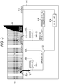
- the electrodes 111-1 to 111-4 have contact with liquid 131 ( Fig. 3 ) in the petri dish 11 including molded resin, measure an action potential of a specimen in the liquid 131, and respectively transmit the action potentials to the amplifiers 112-1 to 112-4. Furthermore, the electrode 111-11 supplies a reference potential generated by the reference potential generating unit 119 to the liquid 131.
- the amplifiers 112-1 to 112-4 are respectively provided directly below the electrodes 111-1 to 111-4 in the single substrate and respectively amplify voltages detected by the electrodes 111-1 to 111-4 and output the detected voltages to the switches 113-1 to 113-4.
- the switches 113-1 and 113-2 are controlled to be turned on or off by the transfer controller 115. When being turned on, the switches 113-1 and 113-2 output outputs from the amplifiers 112-1 and 112-2 to the output unit 116 via the vertical transfer line 114-1.
- the switches 113-3 and 113-4 are controlled to be turned on or off by the transfer controller 115. When being turned on, the switches 113-3 and 113-4 output outputs from the amplifiers 112-3 and 112-4 to the output unit 116 via the vertical transfer line 114-2.
- the output unit 116 converts amplified signals supplied from the amplifiers 112-1 to 112-4 via the vertical transfer lines 114-1 and 114-2 into digital signals and outputs the digital signals from the terminals 117-1 to 117-4.
- the terminals 118-1 and 118-2 receive power and the like supplied from outside.
- the reference potential generating unit 119 generates the reference potential and supplies the reference potential to the liquid 131 by the electrode 111-11.
- the electrode 111-11 has contact with the liquid 131 ( Fig. 3 ) in the petri dish 11 including molded resin and supplies the reference potential to the liquid 131.
- the electrodes 111-1 and 111-11 respectively include plating portions 151-1 and 151-11 including platinum and the like and metal portions 152-1 and 152-11.
- the electrode 111 includes only the metal portion 152 in general. However, since the metal portion 152 is a portion having contact with the liquid 131, the plating portion 151 is provided to prevent corrosion and the like.
- the electrode 111-1 is an electrode which reads a signal, is connected to a gate of the amplifier 112 including an amplifying transistor, and transmits a potential of the liquid 131.
- the amplifier 112 includes an amplifying transistor, and a source and a drain of the amplifying transistor are connected to a power source VDD.
- the amplifier 112 outputs a voltage according to a potential V supplied from the electrode 111-1 to the gate to the output unit 116.
- the output unit 116 analog-digital converts the output voltage which is the analog signal from the amplifier 112 and outputs the digital signal from the terminal 117.
- the electrode 111-11 is an electrode which applies the reference potential output from the reference potential generating unit 119 to the liquid 131.
- Breakers 191-1 and 191-2 are provided between the respective electrodes 111-1 and 111-11 and the power source VDD.
- the breakers 191-1 and 191-2 are connected to the power source VDD when the plating processing is performed on the electrodes 111-1 and 111-11 at the time of manufacturing and apply the voltage of the power source VDD to the electrodes 111-1 and 111-11 to form the plating portions 151-1 and 151-2.
- the breakers 191-1 and 191-2 measure potentials by the electrode 111-1, and when the reference potential is output by the electrode 111-11, the breakers 191-1 and 191-2 are in a high-impedance state and block conduction between the power source VDD and the electrodes 111-1 and 111-11.
- the power source VDD which exists at the subsequent stage of the breakers 191-1 and 191-2 is a necessary component for an electrode plating process for forming the plating portions 151-1 and 151-2 at the time of manufacturing.
- signal transmission characteristics are deteriorated due to a capacitance caused by being parasitic in a circuit for applying voltages to the electrodes 111-1 and 111-11. Therefore, after the manufacturing, by blocking the conduction between the power source VDD and the electrodes 111-1 and 111-11, the breakers 191-1 and 191-2 prevent the deterioration in the signal transmission characteristics.
- each of the breakers 191-1 and 191-2 is connected to the power source VDD.
- the electrodes 111-1 and 111-11 may be ground potentials in the electrode plating process. Therefore, in this case, the breakers 191-1 and 191-2 may be controlled to be turned on or off relative to the ground.
- the breakers 191-1 and 191-2 respectively include Field Effect Transistor (FET) switches 2111-1 and 211-2.
- FET Field Effect Transistor
- the petri dish 11 is filled with plating solution 221, and in addition, the FET switches 211-1 and 211-2 are controlled to be turned on. With this operation, as indicated by an alternate long and short dash line, the voltage of the power source VDD is applied to the electrodes 111-1 and 111-11. As a result, the plating processing is performed on the plating solution 221 on the metal portions 152-1 and 152-11 of the respective electrodes 111-1 and 111-11, and the plating portions 151-1 and 151-11 are formed.
- the petri dish 11 is filled with the liquid 131 in which the specimens are input, and the FET switches 211-1 and 211-2 are turned off.
- the potential of the power source VDD is blocked relative to the electrodes 111-1 and 111-11, and as indicated by a heavy line, the potential V is transmitted by the electrode 111-11, and the electrode 111-1 outputs the reference potential.
- the voltage from the power source VDD is not applied to the gate of the amplifier 112, and the signal from the electrode 111-1 is appropriately transmitted. Therefore, the deterioration in the signal transmission characteristics can be prevented.
- the FET switches 211-1 and 211-2 are provided as the specific configurations of the breakers 191-1 and 191-2.
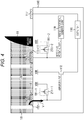
- the specific configurations of the breakers 191-1 and 191-2 may be diodes 231-1 and 231-2.
- anodes of the diodes 231-1 and 231-2 are respectively connected to the electrodes 111-1 and 111-11, and cathodes of the diodes 231-1 and 231-2 are connected to the terminal 118.
- a voltage with a potential lower than the potential of the plating solution 221 is applied to the terminal 118.
- the potential from the terminal 118 is blocked relative to the electrodes 111-1 and 111-11, and as indicated by a heavy line, the potential V is transmitted by the electrode 111-1, and the electrode 111-11 outputs the reference potential.
- the signal from the electrode 111-1 is appropriately transmitted to the gate of the amplifier 112, the deterioration in the signal transmission characteristics can be prevented.
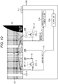
- an impedance of the reference potential generating unit 119 is small. Therefore, as illustrated in Fig. 10 , when a leakage current Ia is generated as indicated by an alternate long and short dash line, there is a possibility that a current to the reference potential generating unit 119 is generated, a potential difference from the reference voltage is generated by an external resistance r to a bias supply unit 171 by the liquid 131, and an input potential to the gate of the amplifying transistor configuring the amplifier 112 differs from the reference potential. Therefore, when the leakage current Ia and the external resistance r vary, the input potential to the gate of the amplifier 112 varies.
- the impedance of the reference potential generating unit 119 is small. Therefore, as illustrated in Fig. 11 , when the leakage current Ia is generated as indicated by an alternate long and short dash line, there is a possibility that the current to the reference potential generating unit 119 is generated, the potential difference from the reference voltage is generated by the external resistance r to the bias supply unit 171 by the liquid 131, and an input potential to the gate of the amplifying transistor configuring the amplifier 112 differs from the reference potential. Therefore, when the leakage current Ia and the external resistance r vary, the input potential to the gate of the amplifier 112 varies.
- a cathode of a diode 251-1 having the same IV conversion characteristics (current voltage conversion characteristics) as the diode 231-1 is connected to a previous stage of the gate of the amplifying transistor configuring the amplifier 112, and an anode is grounded. Furthermore, a cathode of a diode 251-2 having the same characteristics as the diode 231-2 is connected to a previous stage of the reference potential generating unit 119, and an anode is grounded.
- the diodes 231-1 and 251-1 having the equal characteristics are connected in series, and the diodes 231-2 and 251-2 having the equal characteristics are connected in series.
- the leakage currents Ia and Ib indicated by the solid lines are equal to each other, the potentials of the electrodes 111-1 and 111-11 are substantially the same, and the leakage current indicated by the dotted line is not flowed by an internal resistance r. Therefore, the input voltage to the gate of the amplifying transistor configuring the amplifier 112 can be stabilized.
- the input voltage to the gate of the amplifying transistor configuring the amplifier 112 can be stabilized without increasing the number of processes in the manufacturing.
- the power supplied to the breakers 191-1 and 191-2 is external power supplied from the terminal 118 or the power source VDD which has been individually provided.
- the power may be supplied by the power source VDD of the amplifier 112.
- the cathodes of the diodes 231-1 and 231-2 are connected to the power source VDD of the amplifier 112.
- the electrodes 111-1 to 111-4 and 111-11, the amplifiers 112-1 to 112-4, and the reference potential generating unit 119 are formed on the same substrate.
- the electrode 111, the amplifier 112, and the reference potential 119 are formed on the same substrate, a configuration other than the configuration in which the electrodes 111-1 to 111-4 are arranged in two rows and two columns as illustrated in Fig. 2 may be used.
- an electrode configuration in which electrodes are arranged in n rows and m columns may be used.
- the number of electrodes 111-11 used to supply the reference potential may be equal to or more than one.
- a configuration may be used in which an electrode group 111-31 including black electrodes arranged in an array of three rows and three columns and an amplifier group 112-31 of which amplifiers are respectively connected to the electrodes are included, the electrode group 111-31 and the amplifier group 112-31 are connected to a multiplexer (Mux) 271, and the multiplexer 271 time-divisionally outputs output signals.
- Mcux multiplexer
- a configuration may be used in which an electrode group 111-41 including electrodes arranged in an array of three rows and three columns is controlled by the transfer controller 115 in unit of three rows, outputs are transferred to three vertical transfer lines 114-11 to 114-13, are amplified by an amplifier group 112-41 including amplifiers respectively provided on the vertical transfer lines 114-11 to 114-13, and are output to the output unit 116.
- three gray electrodes arranged in the upper and the lower stages in Fig. 9 are controlled to be turned on or off by switches.
- three black electrodes in the middle stage do not have a switch and constantly perform output.
- a configuration may be used in which a lower left black electrode, an upper left electrode, and an upper right electrode, that is, three electrodes in total of the electrode group 111-51 including electrodes arranged in an array of three rows and two columns are respectively connected to three amplifiers of an amplifier group 112-51.
- each electrode included in the electrode group 111-51 includes a local memory denoted with "m" in Fig. 9 .
- the present disclosure may have the following configuration.
Landscapes
- Chemical & Material Sciences (AREA)
- Health & Medical Sciences (AREA)
- Life Sciences & Earth Sciences (AREA)
- Engineering & Computer Science (AREA)
- Physics & Mathematics (AREA)
- General Physics & Mathematics (AREA)
- Electrochemistry (AREA)
- Chemical Kinetics & Catalysis (AREA)
- Analytical Chemistry (AREA)
- Biochemistry (AREA)
- General Health & Medical Sciences (AREA)
- Immunology (AREA)
- Pathology (AREA)
- Molecular Biology (AREA)
- Biomedical Technology (AREA)
- Organic Chemistry (AREA)
- Materials Engineering (AREA)
- Metallurgy (AREA)
- Power Engineering (AREA)
- Biophysics (AREA)
- Automation & Control Theory (AREA)
- Human Computer Interaction (AREA)
- Hematology (AREA)
- Urology & Nephrology (AREA)
- Food Science & Technology (AREA)
- Medicinal Chemistry (AREA)
- Electrodes Of Semiconductors (AREA)
- Electroplating Methods And Accessories (AREA)
- Apparatus Associated With Microorganisms And Enzymes (AREA)
Applications Claiming Priority (2)
| Application Number | Priority Date | Filing Date | Title |
|---|---|---|---|
| JP2016235131 | 2016-12-02 | ||
| PCT/JP2017/041417 WO2018101076A1 (ja) | 2016-12-02 | 2017-11-17 | 半導体装置、および電位測定装置 |
Publications (2)
| Publication Number | Publication Date |
|---|---|
| EP3550296A1 true EP3550296A1 (de) | 2019-10-09 |
| EP3550296A4 EP3550296A4 (de) | 2019-12-18 |
Family
ID=62241568
Family Applications (1)
| Application Number | Title | Priority Date | Filing Date |
|---|---|---|---|
| EP17875259.8A Pending EP3550296A4 (de) | 2016-12-02 | 2017-11-17 | Halbleiterbauelement und potenzialmessvorrichtung |
Country Status (5)
| Country | Link |
|---|---|
| US (1) | US11492722B2 (de) |
| EP (1) | EP3550296A4 (de) |
| JP (1) | JP6987781B2 (de) |
| CN (1) | CN109952505B (de) |
| WO (1) | WO2018101076A1 (de) |
Families Citing this family (2)
| Publication number | Priority date | Publication date | Assignee | Title |
|---|---|---|---|---|
| JP2021096208A (ja) * | 2019-12-19 | 2021-06-24 | ソニーセミコンダクタソリューションズ株式会社 | 電位測定装置 |
| JP2021099229A (ja) * | 2019-12-20 | 2021-07-01 | ソニーセミコンダクタソリューションズ株式会社 | 電位測定装置 |
Family Cites Families (17)
| Publication number | Priority date | Publication date | Assignee | Title |
|---|---|---|---|---|
| US5846708A (en) | 1991-11-19 | 1998-12-08 | Massachusetts Institiute Of Technology | Optical and electrical methods and apparatus for molecule detection |
| JP3193471B2 (ja) | 1992-09-04 | 2001-07-30 | 松下電器産業株式会社 | 一体化複合電極 |
| US6476751B1 (en) * | 2000-03-29 | 2002-11-05 | Photobit Corporation | Low voltage analog-to-digital converters with internal reference voltage and offset |
| JP3909738B2 (ja) | 2000-07-13 | 2007-04-25 | 松下電器産業株式会社 | 細胞外記録用一体化複合電極 |
| JP2004064650A (ja) | 2002-07-31 | 2004-02-26 | Toppan Printing Co Ltd | 携帯端末装置 |
| CN100420139C (zh) * | 2003-09-19 | 2008-09-17 | 株式会社三社电机制作所 | 电镀电源装置 |
| CN1671054B (zh) * | 2004-03-15 | 2010-04-07 | 中芯国际集成电路制造(上海)有限公司 | 用于低非线性度模-数转换器的器件与方法 |
| JP4921255B2 (ja) * | 2007-06-22 | 2012-04-25 | ルネサスエレクトロニクス株式会社 | 逐次型ad変換器 |
| GB0820629D0 (en) | 2008-11-11 | 2008-12-17 | Univ Bath | Biocompatible electrode |
| CN104681079B (zh) * | 2009-11-06 | 2018-02-02 | 株式会社半导体能源研究所 | 半导体装置及用于驱动半导体装置的方法 |
| WO2011153216A2 (en) | 2010-06-01 | 2011-12-08 | The Regents Of The University Of California | Integrated electric field sensor |
| US20140142458A1 (en) | 2011-04-08 | 2014-05-22 | Cyberonics, Inc. | Implantable monitoring device with selectable reference channel and optimized electrode placement |
| JP5796373B2 (ja) * | 2011-06-28 | 2015-10-21 | 大日本印刷株式会社 | 検査用器具および検査用デバイス |
| JP5769020B2 (ja) | 2011-10-25 | 2015-08-26 | 国立大学法人東北大学 | 複数の電極を備えたicチップ |
| JP2013108831A (ja) | 2011-11-21 | 2013-06-06 | Seiko Epson Corp | センサー装置およびセンサー装置の製造方法 |
| CN110023746B (zh) * | 2016-12-02 | 2022-11-18 | 索尼半导体解决方案公司 | 半导体装置和电位测量装置 |
| US11395873B2 (en) | 2017-06-14 | 2022-07-26 | Smith & Nephew, Inc. | Control of wound closure and fluid removal management in wound therapy |
-
2017
- 2017-11-17 WO PCT/JP2017/041417 patent/WO2018101076A1/ja not_active Ceased
- 2017-11-17 US US16/343,611 patent/US11492722B2/en active Active
- 2017-11-17 CN CN201780068778.8A patent/CN109952505B/zh active Active
- 2017-11-17 EP EP17875259.8A patent/EP3550296A4/de active Pending
- 2017-11-17 JP JP2018553776A patent/JP6987781B2/ja active Active
Also Published As
| Publication number | Publication date |
|---|---|
| US11492722B2 (en) | 2022-11-08 |
| JP6987781B2 (ja) | 2022-01-05 |
| JPWO2018101076A1 (ja) | 2019-10-24 |
| US20200048787A1 (en) | 2020-02-13 |
| CN109952505B (zh) | 2022-10-18 |
| CN109952505A (zh) | 2019-06-28 |
| WO2018101076A1 (ja) | 2018-06-07 |
| EP3550296A4 (de) | 2019-12-18 |
Similar Documents
| Publication | Publication Date | Title |
|---|---|---|
| JP4351632B2 (ja) | センサ配置およびセンサ配置の駆動方法 | |
| JP3701241B2 (ja) | センサ配列のトランジスタの状態を検出するセンサ配列および方法 | |
| US10481123B2 (en) | Ion-sensing charge-accumulation circuits and methods | |
| US7019305B2 (en) | Biosensor circuit and sensor array consisting of a plurality of said biosensor circuits and biosensor array | |
| US8702921B2 (en) | Biosensors array and method for operating a biosensor array | |
| CN108291887B (zh) | 电位测量装置 | |
| US10657902B2 (en) | Sensing circuit of display device for sensing pixel current | |
| CN114019006A (zh) | 阵列列积分器 | |
| EP3550296A1 (de) | Halbleiterbauelement und potenzialmessvorrichtung | |
| KR102347625B1 (ko) | 메모리에서의 ai를 위한 dac/adc 아키텍처 | |
| CN107076569A (zh) | 用于感测的装置和方法 | |
| Zeng et al. | A 128× 128 current-mode ultra-high frame rate ISFET array for ion imaging | |
| TWI740517B (zh) | 記憶體內計算裝置以及記憶體內計算方法 | |
| EP3550297A1 (de) | Halbleiterbauelement und potenzialmessvorrichtung | |
| US10073052B2 (en) | Ion concentration sensor | |
| US11468146B2 (en) | Array of integrated pixel and memory cells for deep in-sensor, in-memory computing | |
| CN105263404B (zh) | 信号检测装置、信号检测方法、以及信号检测装置的制造方法 | |
| US20230003678A1 (en) | Potential measurement device | |
| JP2011222547A (ja) | テストエレメントグループおよび半導体装置 | |
| WO2024091986A1 (en) | Electrochemical systems with massively parallel array of controllable electrochemical cells and sensor system for sparse sensing | |
| EP4681183A1 (de) | Sensor und verfahren zum betreiben eines sensors | |
| HK40060883A (en) | Nanopore sequencing circuit, sequencing method and device | |
| US20170040377A1 (en) | Sensing device |
Legal Events
| Date | Code | Title | Description |
|---|---|---|---|
| STAA | Information on the status of an ep patent application or granted ep patent |
Free format text: STATUS: THE INTERNATIONAL PUBLICATION HAS BEEN MADE |
|
| PUAI | Public reference made under article 153(3) epc to a published international application that has entered the european phase |
Free format text: ORIGINAL CODE: 0009012 |
|
| STAA | Information on the status of an ep patent application or granted ep patent |
Free format text: STATUS: REQUEST FOR EXAMINATION WAS MADE |
|
| 17P | Request for examination filed |
Effective date: 20190624 |
|
| AK | Designated contracting states |
Kind code of ref document: A1 Designated state(s): AL AT BE BG CH CY CZ DE DK EE ES FI FR GB GR HR HU IE IS IT LI LT LU LV MC MK MT NL NO PL PT RO RS SE SI SK SM TR |
|
| AX | Request for extension of the european patent |
Extension state: BA ME |
|
| A4 | Supplementary search report drawn up and despatched |
Effective date: 20191114 |
|
| RIC1 | Information provided on ipc code assigned before grant |
Ipc: G01N 27/27 20060101ALI20191108BHEP Ipc: G01N 27/416 20060101AFI20191108BHEP Ipc: H03F 1/52 20060101ALI20191108BHEP Ipc: H01L 27/02 20060101ALI20191108BHEP Ipc: G01N 27/30 20060101ALI20191108BHEP Ipc: G01N 33/487 20060101ALI20191108BHEP Ipc: G01N 33/483 20060101ALI20191108BHEP Ipc: C25D 21/12 20060101ALI20191108BHEP Ipc: C25D 7/12 20060101ALI20191108BHEP Ipc: G01N 33/543 20060101ALI20191108BHEP Ipc: G01R 29/12 20060101ALI20191108BHEP |
|
| DAV | Request for validation of the european patent (deleted) | ||
| DAX | Request for extension of the european patent (deleted) | ||
| STAA | Information on the status of an ep patent application or granted ep patent |
Free format text: STATUS: EXAMINATION IS IN PROGRESS |
|
| 17Q | First examination report despatched |
Effective date: 20220414 |
|
| STAA | Information on the status of an ep patent application or granted ep patent |
Free format text: STATUS: THE APPLICATION IS DEEMED TO BE WITHDRAWN |