EP3546822A1 - Mikrospiegel aufweisendes lichtmodul für einen kraftfahrzeugscheinwerfer - Google Patents
Mikrospiegel aufweisendes lichtmodul für einen kraftfahrzeugscheinwerfer Download PDFInfo
- Publication number
- EP3546822A1 EP3546822A1 EP19161297.7A EP19161297A EP3546822A1 EP 3546822 A1 EP3546822 A1 EP 3546822A1 EP 19161297 A EP19161297 A EP 19161297A EP 3546822 A1 EP3546822 A1 EP 3546822A1
- Authority
- EP
- European Patent Office
- Prior art keywords
- housing
- light module
- micromirrors
- light
- dust
- Prior art date
- Legal status (The legal status is an assumption and is not a legal conclusion. Google has not performed a legal analysis and makes no representation as to the accuracy of the status listed.)
- Granted
Links
Images




Classifications
-
- F—MECHANICAL ENGINEERING; LIGHTING; HEATING; WEAPONS; BLASTING
- F21—LIGHTING
- F21S—NON-PORTABLE LIGHTING DEVICES; SYSTEMS THEREOF; VEHICLE LIGHTING DEVICES SPECIALLY ADAPTED FOR VEHICLE EXTERIORS
- F21S41/00—Illuminating devices specially adapted for vehicle exteriors, e.g. headlamps
- F21S41/20—Illuminating devices specially adapted for vehicle exteriors, e.g. headlamps characterised by refractors, transparent cover plates, light guides or filters
- F21S41/25—Projection lenses
-
- F—MECHANICAL ENGINEERING; LIGHTING; HEATING; WEAPONS; BLASTING
- F21—LIGHTING
- F21S—NON-PORTABLE LIGHTING DEVICES; SYSTEMS THEREOF; VEHICLE LIGHTING DEVICES SPECIALLY ADAPTED FOR VEHICLE EXTERIORS
- F21S41/00—Illuminating devices specially adapted for vehicle exteriors, e.g. headlamps
- F21S41/20—Illuminating devices specially adapted for vehicle exteriors, e.g. headlamps characterised by refractors, transparent cover plates, light guides or filters
- F21S41/29—Attachment thereof
- F21S41/295—Attachment thereof specially adapted to projection lenses
-
- F—MECHANICAL ENGINEERING; LIGHTING; HEATING; WEAPONS; BLASTING
- F21—LIGHTING
- F21S—NON-PORTABLE LIGHTING DEVICES; SYSTEMS THEREOF; VEHICLE LIGHTING DEVICES SPECIALLY ADAPTED FOR VEHICLE EXTERIORS
- F21S41/00—Illuminating devices specially adapted for vehicle exteriors, e.g. headlamps
- F21S41/30—Illuminating devices specially adapted for vehicle exteriors, e.g. headlamps characterised by reflectors
- F21S41/32—Optical layout thereof
- F21S41/36—Combinations of two or more separate reflectors
-
- F—MECHANICAL ENGINEERING; LIGHTING; HEATING; WEAPONS; BLASTING
- F21—LIGHTING
- F21S—NON-PORTABLE LIGHTING DEVICES; SYSTEMS THEREOF; VEHICLE LIGHTING DEVICES SPECIALLY ADAPTED FOR VEHICLE EXTERIORS
- F21S41/00—Illuminating devices specially adapted for vehicle exteriors, e.g. headlamps
- F21S41/30—Illuminating devices specially adapted for vehicle exteriors, e.g. headlamps characterised by reflectors
- F21S41/32—Optical layout thereof
- F21S41/36—Combinations of two or more separate reflectors
- F21S41/365—Combinations of two or more separate reflectors successively reflecting the light
-
- F—MECHANICAL ENGINEERING; LIGHTING; HEATING; WEAPONS; BLASTING
- F21—LIGHTING
- F21S—NON-PORTABLE LIGHTING DEVICES; SYSTEMS THEREOF; VEHICLE LIGHTING DEVICES SPECIALLY ADAPTED FOR VEHICLE EXTERIORS
- F21S41/00—Illuminating devices specially adapted for vehicle exteriors, e.g. headlamps
- F21S41/60—Illuminating devices specially adapted for vehicle exteriors, e.g. headlamps characterised by a variable light distribution
- F21S41/67—Illuminating devices specially adapted for vehicle exteriors, e.g. headlamps characterised by a variable light distribution by acting on reflectors
- F21S41/675—Illuminating devices specially adapted for vehicle exteriors, e.g. headlamps characterised by a variable light distribution by acting on reflectors by moving reflectors
-
- F—MECHANICAL ENGINEERING; LIGHTING; HEATING; WEAPONS; BLASTING
- F21—LIGHTING
- F21S—NON-PORTABLE LIGHTING DEVICES; SYSTEMS THEREOF; VEHICLE LIGHTING DEVICES SPECIALLY ADAPTED FOR VEHICLE EXTERIORS
- F21S45/00—Arrangements within vehicle lighting devices specially adapted for vehicle exteriors, for purposes other than emission or distribution of light
- F21S45/10—Protection of lighting devices
-
- F—MECHANICAL ENGINEERING; LIGHTING; HEATING; WEAPONS; BLASTING
- F21—LIGHTING
- F21S—NON-PORTABLE LIGHTING DEVICES; SYSTEMS THEREOF; VEHICLE LIGHTING DEVICES SPECIALLY ADAPTED FOR VEHICLE EXTERIORS
- F21S45/00—Arrangements within vehicle lighting devices specially adapted for vehicle exteriors, for purposes other than emission or distribution of light
- F21S45/40—Cooling of lighting devices
- F21S45/47—Passive cooling, e.g. using fins, thermal conductive elements or openings
-
- F—MECHANICAL ENGINEERING; LIGHTING; HEATING; WEAPONS; BLASTING
- F21—LIGHTING
- F21W—INDEXING SCHEME ASSOCIATED WITH SUBCLASSES F21K, F21L, F21S and F21V, RELATING TO USES OR APPLICATIONS OF LIGHTING DEVICES OR SYSTEMS
- F21W2102/00—Exterior vehicle lighting devices for illuminating purposes
-
- F—MECHANICAL ENGINEERING; LIGHTING; HEATING; WEAPONS; BLASTING
- F21—LIGHTING
- F21W—INDEXING SCHEME ASSOCIATED WITH SUBCLASSES F21K, F21L, F21S and F21V, RELATING TO USES OR APPLICATIONS OF LIGHTING DEVICES OR SYSTEMS
- F21W2107/00—Use or application of lighting devices on or in particular types of vehicles
- F21W2107/10—Use or application of lighting devices on or in particular types of vehicles for land vehicles
Definitions
- the present invention relates to a light module for a motor vehicle headlight according to the preamble of claim 1.
- a light module is known from DE 198 22 142 C2 known and has a light source, a primary optics, an array of micromirrors whose mirror position is controlled and a secondary optics, which has at least one secondary optics lens.
- the light source, the primary optics, the arrangement of micromirrors and the secondary optics are arranged relative to each other so that light emanating from the light source and directed by the primary optics on the arrangement of micromirrors, from the arrangement of micromirrors on the refractive secondary optics is reflected ,
- the arrangement of micromirrors is part of a DMD chip (digital mirror device).
- DMD chips can have a large number (greater than one million) of micromirrors exhibit.
- Each individual micromirror is, for example, only 8 x 8 microns in size.
- One position of each individual micromirror can be switched between two positions. In one position he reflects the incident light to the secondary optics, and in the other position he reflects the light, for example, on an absorber.
- the secondary optics form the arrangement of the micromirrors in the apron of the light module, which is in the case of a motor vehicle headlight, for example, on the roadway from.
- Micro mirrors that reflect light onto the secondary optics appear as bright pixels in the light distribution resulting from the image, whereas the micromirrors that reflect light onto the absorber appear as dark pixels in the light distribution.
- the shape of the light distribution with a given by the number of pixels and thus by the number of micromirrors fineness is controllable, which allows, for example, camera-controlled light distributions, in which areas that would dazzle other road users, can be specifically darkened and other areas For example, traffic signs or pedestrians, are specifically illuminated so that they are recognized by the driver.
- the object of the invention is to provide a light module of the type mentioned, whose light distributions do not have the disadvantageous dark spots and blurred images.
- the light module according to the invention is characterized in that the light module is a dust-tight Interior and that the light source, the primary optics and the arrangement of micromirrors are arranged in the dust-tight interior.
- the invention is based on the finding that the locally undesirable dark spots and blurred images of individual micromirrors are produced by dust particles which are located in the beam path of the light, in particular between the arrangement of the micromirrors and the secondary optics.
- the size of dust particles is between 0.1 microns and 100 microns.
- a typical construction volume of a light module is 0.2 mx 0.2 mx 0.1 m. It has been found that smaller particles, for example 0.5 micron particles, lead to light losses due to blurred images and that particles larger than about 10 microns must be kept completely out of the beam path.
- the dust-free interior is preferably IP6K2 rated.
- the assembly of the components of the light modules involved in the dust-tight sealing of the interior is preferably carried out in a clean room.
- a preferred embodiment is characterized in that the dust-tight interior is enclosed by a front housing part, a central support element, a DMD chip, a first printed circuit board, the secondary optics lens and by a dust-tight pressure compensation membrane. This already existing components are used for sealing.
- the housing front part has a housing window in a part of the housing front part, which faces the first printed circuit board, which is covered dust-tight by the first printed circuit board.
- This embodiment allows electrical contact the first circuit board, which is completely in the dust-tight interior except for the housing window covering surface area, without the circuit board or a wiring harness through a sealing surface (ie by a surface in which a seal is located) must be passed.
- the housing front part has a light exit opening, which is covered dust-tight by the secondary optics lens.
- the dust-proof interior must inevitably have a transparent window through which the light can escape from the interior. Using the secondary optics lens for this feature eliminates the need for an additional window, eliminating light losses and reducing complexity and component count.
- a further preferred embodiment is characterized in that the housing front part has a pressure compensation opening which is covered by the dust-tight pressure compensation membrane, wherein the pressure compensation membrane is gas-permeable. This embodiment allows a pressure equalization despite the difficult due to the dust-tight seal particle exchange between the interior and its surroundings.
- the central carrier element has a carrier element window whose opening is covered by a DMD chip carrying the arrangement of the micromirrors. This feature allows an arrangement of the micromirror-carrying front in the dust-tight outer space, while the electrical contact can be made by a completely outside the interior lying second circuit board.
- the DMD chip is arranged on a rear side of the central carrier element facing away from the interior, wherein the arrangement of micromirrors is arranged in front of the opening of the carrier element window.
- the DMD chip itself is used for sealing, which reduces the complexity of the structure.
- a further preferred refinement is characterized in that the central carrier element has an interior-side flange region which runs along a closed spatial curve, and in that the housing front part has a housing flange region whose shape is a negative of the shape of the flange region of the central carrier element that, when the front part of the housing and the central support element are joined together, the two flange areas contact one another over the entire length of the spatial curve of the flange area or contact a seal lying between them in a planar manner.
- a seal is located on an inner space-side edge of the housing window over the entire length of the edge of the housing window.
- the housing front part consists of plastic and that the seals and sealing lips formed on flange regions of the front part of the housing are made of sealing material.
- FIG. 1 a section through an embodiment of a light module according to the invention 10 of a motor vehicle headlight.
- the light module has a light source 12, a primary optics 14, a DMD chip 16 and a secondary optics 18.
- the light source 12 is a semiconductor light source which is arranged on a first printed circuit board 20 and which emits light 22 in the direction of the primary optics 14.
- the primary optics 14 has a refractive part 14.1 and a reflector 14.2.
- the refractive part 14.1 is illuminated by the light source 12 and directs the light 22 to the reflector 14.2.
- the reflector 14.2 deflects the light 22 incident thereon from the refractive part 14.1 onto a reflecting surface of a front side 16.1 of the DMD chip 16, the reflecting surface consisting of a multiplicity of micromirrors. It is essential that the primary optics direct the light from the light source onto the DMD chip. How and with which optical elements this is done in detail is not essential to the invention.
- a pivot position of the micromirrors can be switched individually for each micromirror or at least for a subset of the micromirrors between a first pivot position and a second pivot position.
- Each micromirror, which is in the first pivot position deflects the light incident on it from the primary optics 14 to the secondary optics 18.
- Each micromirror, which is in the second pivot position is located, deflects the light 22 incident on it from the primary optics 14 so that this light 22.1 does not fall on the secondary optics 18.
- This light 22.1 is directed, for example, onto an absorber 24 and absorbed there, so that it can not produce disturbing light effects.
- the secondary optics 18 directs the light 22 incident on them from the DMD chip 16 into the apron of the light module 10. When the light module is used as intended, this light 22 illuminates the road ahead of the motor vehicle.
- the secondary optics 18 has a secondary optic lens 18.1 of transparent plastic or glass.
- the secondary optics 18 may also have a plurality of lenses, for example an arrangement of an achromatic lens and an imaging lens.
- the path of the light 22 from the light source 12 to its exit from the secondary optics 18 through the secondary optics 18 lies completely in a dust-tightly sealed interior space 26.
- This interior space 26 is replaced by a housing front part 28, a central support element 30 , the DMD chip 16, the first circuit board 20, the secondary optics 18 and a dust-tight pressure compensation membrane 32 limited.
- the central support element 30 has a front side 30.1 facing the inner space 26 and a rear side 30.2.
- the central carrier element 30 has a light source and primary optics side first portion 30.3 and a DMD chip side second portion 30.4. These two sections 30.3 and 30.4 are spatially separated from each other, but are cohesively cohesive and together form the one-piece central support member 30.
- the two sections 30.3 and 30.4 close an angle which is greater than 90 ° but less than 180 °.
- the central support element 30 is preferably made of metal and also serves as a heat sink, which absorbs the heat released in the light source 12 and emits heat to the surroundings of the light module 10.
- the first circuit board 20 is fixedly connected to the front side 30.1 of the central support element 30 in its first portion 30.3.
- the connection is for example a screw and / or adhesive connection.
- a front side 20.1 of the first printed circuit board 20 carries the light source 12 realized as a semiconductor light source and the primary optics 14.
- a rear side 20.2 of the first printed circuit board 20 faces the front side 30.1 of the central support element 30.
- the central carrier element 30 In directions transverse to the front side 20. 1 and toward the rear side 20. 2 of the first printed circuit board 20, the central carrier element 30 protrudes beyond the first printed circuit board 20. These directions are also referred to below as lateral directions 34.
- An example of a lateral direction 34 is in FIG FIG. 1 specified. Other lateral directions are perpendicular to the plane of the drawing.
- the laterally projecting edge of the front side 30. 1 of the central carrier element 30 forms part of an interior-side flange region 30. 5 of the central carrier element 30.
- the second subregion 30. 4 of the central carrier element 30 has a carrier element window 35.
- a window edge area surrounding the carrier element window 35 forms a window flange area 36 on the rear side 30.2 of the central carrier element 30.
- the DMD chip 16 is arranged on the rear side 30.2 of the central carrier element 30 in its second partial area 30.4 such that it surrounds the carrier element window 35 covers.
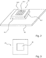
- the DMD chip 16 has two broad sides in the form of a front 16.1 and a back, the front and back sides are separated by lying between them lateral narrow sides 16.3. In this case, its front side 16.1 carrying the micromirrors 16.4 faces the support element window 35 and thus the interior 26.
- the front side 16. 1 of the DMD chip 16 has a central chip area in which the micromirrors 16. 4 are arranged, and it has a flange area 16. 5 surrounding the central chip area in a closed curve, in which no micromirrors 16. 4 are arranged.
- the number of micromirrors is about 1.3 million, arranged in a matrix of 1152 columns and 1152 rows.
- Such DMD chips digital mirror device
- Such DMD chips are manufactured and sold, for example, by the company Texas Instruments.
- FIG. 1 and FIG. 2 show in combination with each other that the DMD chip 16 is arranged in total so that the two flange portions 36 and 16.5 are opposed to each other. Between the two flange portions 36 and 16.5 is a DMD chip seal 38 in the form of a flat gasket, which is held by the flange portions 36 and 16.5 with these flange portions pressing together pressing force and rotates the support member window 35 in a closed curve.
- FIG. 2 also shows that the DMD chip 16 is arranged and held in a socket 40.1 of a second printed circuit board 40.
- the mechanical support of the DMD chip 16 in the base 40.1 on the lateral narrow sides 16.3 and possibly additionally on parts of the back of the DMD chip 16, and the electrical contact is also made on the side Narrow sides 16.3 and / or over the back of the DMD chip 16.
- the second circuit board 40 is fixedly connected to the second portion 30.4 of the central support member 30.
- the compound is preferably carried out as an adhesive bond. In the FIG. 1 this is represented by the contact of the second circuit board 40 by screw domes 30.6 of the central support element.
- the second printed circuit board 40 does not exert the pressing force acting perpendicular to the surface of the second printed circuit board 40 and the front side 16.1 of the DMD chip 16.
- the second circuit board 40 holds the DMD chip 16 with its socket tangentially to the front 16.1 of the DMD chip 16 and the second circuit board 40 facing directions.
- the second circuit board 40 is completely outside the sealed interior 26.
- a central area of the back side of the DMD chip 16 serves as an interface for dissipating heat from the DMD chip 16 and therefore has no electrical connections.
- FIG. 3 schematically shows a plan view of the second circuit board 40 with a circuit board window 42.
- the opening of the circuit board window 42 is in the assembled state, the no electrical connections having central area of the back of the DMD chip 16 opposite.
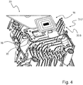
- FIG. 4 shows an oblique view of the back 30.2 of a central support member 30 prior to assembly of the DMD chip 16.
- the central support member 30 has on its rear side 30.2 a the carrier element window 35 in a closed curve encircling outer flange portion which in the FIG. 4 is covered by the DMD chip seal 38.
- the contours of the DMD chip seal 38 correspond to the Contours of the outer flange portion and the support member window 35th
- FIG. 4 also shows screw domes 30.6, with the help of the DMD chip 16 is pressed by additional components on the DMD chip seal 38. As a result, the sealing function is ensured, and the DMD chip 16 is additionally fixed in its end position.
- FIG. 1 shows how the force acting perpendicular to the front 16.1 and the back of the DMD chip 16 pressing force generated by an elastic member 44 and a punch 46 by the in FIG. 3 shown printed circuit board window 42 is applied to the central part of the back of the DMD chip 16.
- the elastic member 44 has a proximal portion 44.1 and two distal ends 44.2 with respect to the punch 46.
- the distal ends 44. 2 are rigidly connected to the central carrier element 30, in particular to its second subarea 30. 4.
- the proximal region 44.1 is positively and / or positively connected to a first end 46.1 of the punch 46.
- a second end 46.2 of the punch 46 is biased against the back of the DMD chip 16.
- the bias corresponds to a restoring force of the elastic member 44, which is generated by elastic deformation of the elastic member 44 in the assembly of the light module 10.
- the screw domes 30.6 are preferably used in addition to the attachment of the distal ends 44.2 of the elastic member 44 to the central support member 30.
- the DMD chip 16 is held tangentially to its broad sides by the base 40.1 and thus by the second printed circuit board 42.
- the pressing force generated by the elastic element 44 is simultaneously exerted on the DMD chip seal 38, which contributes to the dust-tight sealing of the interior 26.
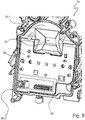
- FIG. 5 schematically shows a plan view of the front side 30.1 of the central support member 30 with the first circuit board 20, carrier element window 35 and an inner side flange portion 30.5 of the central support member 30 which has the shape of a closed curve.
- the curve lies in the in the FIG. 1 illustrated embodiment in which the two portions 30.3 and 30.4 form an angle with each other, which is greater than 90 ° and less than 180 °, not in a plane.
- the curve can, depending on the design, but also run in a plane. In any case, the curve forms a curve running in space and therefore spatial.
- a flat gasket or a flange reinforcement 50 can rest, which runs around the housing window 48 of the housing front part in the assembled state with the housing front part 28.
- FIG. 6 shows this to the central support member 30 FIG. 5 complementary housing front part 28.
- the housing front part 28 has a housing flange region 28.1, the shape of which is a negative of the shape of the flange region 30.5 of the central support element 30, so that both flange regions 28.1, 30.5 are joined together when the housing front part 28 and of the central support member 30 along the entire length of the spatial curve of the flange portion 30.5 surface contact or touching a lying seal between them each surface.
- On the housing flange portion 28.1 is located over the entire length of a seal 52. Over the length of the edge of the housing window 48 is on the edge of a seal 54.
- the seals 52 and 54 are preferably sealing lips made of sealing material, which is integrally formed on the preferably made of plastic housing front part 28.
- the sealing material is for example a plastically deformable plastic, for example silicone. Silicone has the advantage that it can be baked out prior to assembly, which avoids any subsequent impairment of optical surfaces of the light module 10 by precipitation of vaporized sealing material.
- the projection module 10 preferably has screw connections, with which the flange portions 30.5 and 28.1 are pressed against one another. In the assembled state, the housing front part 28 and the central support element 30 surround the interior 26.
- FIG. 1 lies at least the back 20.2 of the first circuit board 20, which faces the interior side front side 30.1 of the central support member 30, in the interior 26.
- a the light source 12 and the primary optics 14-bearing front 20.1 of the first Printed circuit board 20 faces the front housing part 28.
- the housing front part 28 has a housing window 48 in a part of the housing front part 20, which faces the first printed circuit board 20.
- the housing window allows an electrical connection of the electrical components, in particular the light source 12, arranged in the dust-tightly sealed interior 26 of the light module 10, with a cable harness 29 brought up from the outside.
- the edge of the housing window 48 forms on its side facing the first circuit board 20 a Gesimouserousflansch, the surface of the first printed circuit board 20 over its entire length or touched at least over its entire length across the opening of the window circumferential seal 54 surface, the in turn, over its entire length, the first circuit board 20 touched flat.
- the first circuit board 20 covers the housing window 48 dustproof.
- the shape of the front housing part is matched to the position of the first circuit board 20 on the central support member 30 so that a contact between the first circuit board 20 and the Genzouserousflansch, or between the first circuit board 20, the seal 54 and the GeHouseivelyflansch already done if between the housing flange portion 28.1 and the inner side flange portion 30.5 of the central support member 30 is still a small distance.
- the narrow side of the first printed circuit board 20 that extends around the broad sides of the first printed circuit board 20 lies in its entire length within the inner space 26.
- the electrical contacting does not have to run in a sealing plane, which improves the reliability of the sealing.
- the housing front part 28 on a light exit opening 56 The width of the light exit opening 56 encircling edge of the front part of the housing is configured as an inner sealing region 58 of the front housing part 28.
- the inner sealing region 58 is also covered with sealing material.
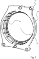
- FIG. 7 shows a mounting piece 60 which serves to hold a secondary optic lens in the front housing part 28.
- the attachment piece 60 has an outer sealing region 62, the shape of which is a negative of the inner sealing region 58 of the front part of the housing 28.
- An opening 64 in the attachment piece 60 and the edge that surrounds this opening 64 have a shape that corresponds to the shape of an edge region of the secondary optic lens so far that the attachment piece 60 receives the secondary optic lens in the opening 64 in a form-fitting manner.
- An inner edge of the attachment piece 60, which orbits the opening 64 of the attachment piece, is designed as an inner sealing area 65.
- the inner sealing region 65 is also covered with sealing material.
- FIG. 8 shows the front housing part 28 with its inner sealing portion 58 from the front.
- the attachment piece 60 is in the assembly of the front and thus against the Light exit direction is inserted into the light exit opening 56 of the front housing part 28 and attached to the front housing part 28.
- the attachment is done for example with screw.
- a further opening 68 in the front housing part 28 is covered by a dust-tight, but gas-permeable and water vapor-permeable pressure equalizing membrane 70, which allows a pressure equalization between the sealed interior 26 and the surroundings of the light module 10.
- FIG. 9 shows the attachment piece 60 with inserted secondary lens 18.1 and housing front part 28.
- the secondary lens 18.1 covers the remaining opening 64 of the attachment piece 60, and the connection of attachment piece and 60 and secondary lens 18.1 is sealed with sealing material of the inner sealing portion 65 of the attachment piece 60.
- the attachment piece 60 fixes the position of the secondary optic lens 18.1 in the one direction of an optical axis of the secondary optics 18 by a collar projecting radially into the opening 64 in a form-fitting manner (cf. Fig. 7 ,
- a lens holder not shown in the figures detects a front edge of the secondary lens 18.1 by positive engagement and determines the position of the secondary lens 18.1 positively in the other direction of the optical axis and thereby exerts an interior 26 directed contact pressure on the secondary lens 18.1 and thus also on the between the secondary optic lens 18.1 and the inner sealing portion 65 of the fixing piece 60 lying sealing material.
- the lens holder is preferably attached to the central support member 30. This can be done for example by screw.
Landscapes
- Engineering & Computer Science (AREA)
- General Engineering & Computer Science (AREA)
- Mechanical Light Control Or Optical Switches (AREA)
- Projection Apparatus (AREA)
Abstract
Description
- Die vorliegende Erfindung betrifft ein Lichtmodul für einen Kraftfahrzeugscheinwerfer nach dem Oberbegriff des Anspruchs 1. Ein solches Lichtmodul ist aus der
DE 198 22 142 C2 bekannt und weist eine Lichtquelle, eine Primäroptik, eine Anordnung von Mikrospiegeln, deren Spiegelstellung steuerbar ist und eine Sekundäroptik auf, die wenigstens eine Sekundäroptiklinse aufweist. Die Lichtquelle, die Primäroptik, die Anordnung von Mikrospiegeln und die Sekundäroptik sind relativ zueinander so angeordnet, dass Licht, das von der Lichtquelle ausgeht und von der Primäroptik auf die Anordnung von Mikrospiegeln gerichtet wird, von der Anordnung von Mikrospiegeln auf die lichtbrechende Sekundäroptik reflektierbar ist. - Die Anordnung von Mikrospiegeln ist Bestandteil eines DMD-Chips (digital mirror device). Solche DMD-Chips können eine große Zahl (größer als eine Million) von Mikrospiegeln aufweisen. Jeder einzelne Mikrospiegel ist dabei zum Beispiel nur 8 x 8 Mikrometer groß. Eine Stellung jedes einzelnen Mikrospiegels ist zwischen zwei Stellungen umschaltbar. In einer Stellung reflektiert er das einfallende Licht auf die Sekundäroptik, und in der anderen Stellung reflektiert er das Licht zum Beispiel auf einen Absorber. Die Sekundäroptik bildet die Anordnung der Mikrospiegel in das Vorfeld des Lichtmoduls, das bei einem Kraftfahrzeugscheinwerfer zum Beispiel auf der Fahrbahn liegt, ab. Mikrospiegel, die Licht auf die Sekundäroptik spiegeln, erscheinen in der aus der Abbildung resultierenden Lichtverteilung als helle Pixel, während die Mikrospiegel, die Licht auf den Absorber spiegeln, in der Lichtverteilung als dunkle Pixel erscheinen. Im Ergebnis ist damit die Form der Lichtverteilung mit einer durch die Zahl der Pixel und damit durch die Zahl der Mikrospiegel vorgegebenen Feinheit steuerbar, was zum Beispiel kameragesteuerte Lichtverteilungen ermöglicht, bei denen Bereiche, die andere Verkehrsteilnehmer blenden würden, gezielt abgedunkelt werden können und andere Bereiche, zum Beispiel Verkehrsschilder oder Fußgänger, gezielt beleuchtet werden, damit sie vom Fahrer erkannt werden.
- Es hat sich gezeigt, dass mit bekannten Lichtmodulen erzeugte Lichtverteilungen lokal dunkle Stellen oder unscharfe Abbildungen einzelner Mikrospiegel aufweisen.
- Die Aufgabe der Erfindung besteht in der Angabe eines Lichtmoduls der eingangs genannten Art, dessen Lichtverteilungen die nachteiligen dunklen Stellen und unscharfen Abbildungen nicht aufweisen.
- Diese Aufgabe wird mit den Merkmalen des Anspruchs 1 gelöst. Das erfindungsgemäße Lichtmodul zeichnet sich dadurch aus, dass das Lichtmodul einen staubdichten Innenraum aufweist und dass die Lichtquelle, die Primäroptik und die Anordnung von Mikrospiegeln in dem staubdichten Innenraum angeordnet sind.
- Damit basiert die Erfindung auf der Erkenntnis, dass die lokal unerwünscht dunklen stellen und unscharfen Abbildungen einzelner Mikrospiegel durch Staubpartikel erzeugt werden, die sich im Strahlengang des Lichtes insbesondere zwischen der Anordnung der Mikrospiegel und der Sekundäroptik befinden. Die Größe von Staubpartikeln liegt zwischen 0,1 Mikrometern und 100 Mikrometern. Ein typisches Bauvolumen eines Lichtmoduls liegt bei 0,2 m x 0,2 m x 0,1 m. Es hat sich gezeigt, dass kleinere Partikel, zum Beispiel 0,5 Mikrometer große Partikel, zu Lichteinbußen durch unscharfe Abbildungen führen und dass Partikel, die größer als etwa 10 Mikrometer sind vollständig aus dem Strahlengang heraus gehalten werden müssen. Die Staubfreiheit des Innenraums entspricht bevorzugt der Schutzklasse IP6K2. Die Montage der an der staubdichten Abdichtung des Innenraums beteiligten Bauteile der Lichtmodule erfolgt bevorzugt in einem Reinraum.
- Eine bevorzugte Ausgestaltung zeichnet sich dadurch aus, dass der staubdichte Innenraum durch ein Gehäusevorderteil, ein zentrales Trägerelement, einen DMD-Chip, eine erste Leiterplatte, die Sekundäroptiklinse und durch eine staubdichte Druckausgleichsmembrane umschlossen wird. Damit werden ohnehin vorhandene Bauteile für die Abdichtung verwendet.
- Bevorzugt ist auch, dass das Gehäusevorderteil in einem Teil des Gehäusevorderteils, welcher der ersten Leiterplatte zugewandt ist, ein Gehäusefenster aufweist, das von der ersten Leiterplatte staubdicht abgedeckt wird. Diese Ausgestaltung erlaubt eine elektrische Kontaktierung der ersten Leiterplatte, die bis auf ihren das Gehäusefenster abdeckenden Oberflächenbereich vollständig im staubdichten Innenraum liegt, ohne dass die Leiterplatte oder ein Kabelbaum durch eine Dichtungsfläche (d.h. durch eine Fläche, in der eine Dichtung liegt) hindurchgeführt werden muss.
- Weiter ist bevorzugt, dass das Gehäusevorderteil eine Lichtaustrittsöffnung aufweist, die durch die Sekundäroptiklinse staubdicht abgedeckt wird. Der staubdichte Innenraum muss zwangsläufig ein transparentes Fenster aufweisen, durch welches das Licht aus dem Innenraum austreten kann. Die Nutzung der Sekundäroptiklinse für diese Funktion macht eine Verwendung eines zusätzlichen Fensters unnötig, was Lichtverluste vermeidet und eine Komplexität und Bauteilezahl reduziert.
- Eine weitere bevorzugte Ausgestaltung zeichnet sich dadurch aus, dass das Gehäusevorderteil eine Druckausgleichsöffnung aufweist, die durch die staubdichte Druckausgleichsmembran abgedeckt wird, wobei die Druckausgleichsmembran gasdurchlässig ist. Diese Ausgestaltung erlaubt einen Druckausgleich trotz des aufgrund der staubdichten Abdichtung erschwerten Teilchenaustausches zwischen Innenraum und dessen Umgebung.
- Bevorzugt ist auch, dass das zentrale Trägerelement ein Trägerelementfenster aufweist, dessen Öffnung von einem die Anordnung der Mikrospiegel tragenden DMD-Chip abgedeckt wird. Dieses Merkmal erlaubt eine Anordnung der die Mikrospiegel tragenden Vorderseite im staubdichten Außenraum, während die elektrische Kontaktierung durch eine vollständig außerhalb des Innenraums liegend zweite Leiterplatte erfolgen kann.
- Weiter ist bevorzugt, dass der DMD-Chip auf einer dem Innenraum abgewandten Rückseite des zentralen Trägerelements angeordnet ist, wobei die Anordnung von Mikrospiegeln vor der Öffnung des Trägerelementfensters angeordnet ist. Damit wird der DMD-Chip selbst zur Abdichtung verwendet, was die Komplexität des Aufbaus reduziert.
- Eine weitere bevorzugte Ausgestaltung zeichnet sich dadurch aus, dass das zentrale Trägerelement einen innenraumseitigen Flanschbereich aufweist, der entlang einer geschlossenen räumlichen Kurve verläuft, und dass das Gehäusevorderteil einen Gehäuse-Flanschbereich aufweist, dessen Form ein Negativ der Form des Flanschbereichs des zentralen Trägerelements ist, so dass sich beide Flanschbereiche bei einem Zusammenfügen des Gehäusevorderteils und des zentralen Trägerelements entlang der gesamten Länge der räumlichen Kurve des Flanschbereichs flächig berühren oder eine zwischen ihnen liegende Dichtung jeweils flächig berühren.
- Bevorzugt ist auch, dass eine Dichtung auf einem innenraumseitigen Rand des Gehäusefensters über die gesamte Länge des Randes des Gehäusefensters liegt.
- Weiter ist bevorzugt, dass das Gehäusevorderteil aus Kunststoff besteht und dass die Dichtungen und an Flanschbereiche des Gehäusevorderteils angeformte Dichtlippen aus Dichtungsmaterial sind.
- Weitere Vorteile ergeben sich aus der nachfolgenden Beschreibung, den Zeichnungen und den Unteransprüchen. Es versteht sich, dass die vorstehend genannten und die nachstehend noch zu erläuternden Merkmale nicht nur in der jeweils angegebenen Kombination, sondern auch in anderen Kombinationen oder in Alleinstellung verwendbar sind, ohne den Rahmen der vorliegenden Erfindung zu verlassen.
- Ausführungsbeispiele der Erfindung sind in den Zeichnungen dargestellt und werden in der nachfolgenden Beschreibung näher erläutert.
- Dabei zeigen, jeweils in schematischer Form:
- Figur 1
- ein Ausführungsbeispiel eines erfindungsgemäßen Lichtmoduls in einem zu einer optischen Achse des Lichtmoduls parallelen Schnitt;
- Figur 2
- einen DMD-Chip;
- Figur 3
- eine zweite Leiterplatte mit einem Leiterplattenfenster;
- Figur 4
- eine Schrägansicht der Rückseite eines zentralen Trägerelements vor der Montage des DMD-Chips;
- Figur 5
- eine Draufsicht auf die Vorderseite eines zentralen Trägerelements mit erster Leiterplatte, Trägerelementfenster und einem innenraumseitigen Flanschbereich des zentralen Trägerelements;
- Figur 6
-
Figur 6 zeigt ein zu dem zentralen Trägerelement ausFigur 5 komplementäres Gehäusevorderteil; - Figur 7
- ein Befestigungsstück, das zur Halterung einer Sekundäroptiklinse in dem Gehäusevorderteil dient;
- Figur 8
- das Gehäusevorderteil mit einem inneren Dichtbereich von vorn; und
- Figur 9
- das Befestigungsstück mit eingesetzter Sekundäroptiklinse.
- Dabei bezeichnen gleiche Bezugszeichen in verschiedenen Figuren jeweils gleiche oder zumindest ihrer Funktion nach vergleichbare Elemente.
- Im Einzelnen zeigt die
Figur 1 einen Schnitt durch ein Ausführungsbeispiel eines erfindungsgemäßen Lichtmoduls 10 eines Kraftfahrzeugscheinwerfers. Das Lichtmodul weist eine Lichtquelle 12, eine Primäroptik 14, einen DMD-Chip 16 und eine Sekundäroptik 18 auf. Die Lichtquelle 12 ist eine Halbleiterlichtquelle, die auf einer ersten Leiterplatte 20 angeordnet ist und die Licht 22 in Richtung zu der Primäroptik 14 abstrahlt. Die Primäroptik 14 weist einen lichtbrechenden Teil 14.1 und einen Reflektor 14.2 auf. Der lichtbrechende Teil 14.1 wird von der Lichtquelle 12 beleuchtet und richtet das Licht 22 auf den Reflektor 14.2. Der Reflektor 14.2 lenkt das auf ihn vom lichtbrechenden Teil 14.1 her einfallende Licht 22 auf eine spiegelnde Fläche einer Vorderseite 16.1 des DMD-Chips 16, wobei die spiegelnde Fläche aus einer Vielzahl von Mikrospiegeln besteht. Wesentlich ist dabei, dass die Primäroptik das Licht der Lichtquelle auf den DMD-Chip richtet. Wie und mit welchen optischen Elementen dies im Einzelnen geschieht, ist für die Erfindung nicht wesentlich. - Eine Schwenkstellung der Mikrospiegel ist individuell für jeden Mikrospiegel oder zumindest für eine Teilmenge der Mikrospiegel zwischen einer ersten Schwenkstellung und einer zweiten Schwenkstellung umschaltbar. Jeder Mikrospiegel, der sich in der ersten Schwenkstellung befindet, lenkt das auf ihn von der Primäroptik 14 her einfallende Licht auf die Sekundäroptik 18 um. Jeder Mikrospiegel, der sich in der zweiten Schwenkstellung befindet, lenkt das auf ihn von der Primäroptik 14 her einfallende Licht 22 so ab, dass dieses Licht 22.1 nicht auf die Sekundäroptik 18 fällt. Dieses Licht 22.1 wird zum Beispiel auf einen Absorber 24 gelenkt und dort absorbiert, so dass es keine störenden Lichteffekte erzeugen kann.
- Die Sekundäroptik 18 richtet das auf sie von dem DMD-Chip 16 her einfallende Licht 22 in das Vorfeld des Lichtmoduls 10. Bei einer bestimmungsgemäßen Verwendung des Lichtmoduls wird mit diesem Licht 22 die vor dem Kraftfahrzeug liegende Fahrbahn ausgeleuchtet. Die Sekundäroptik 18 weist eine Sekundäroptiklinse 18.1 aus transparentem Kunststoff oder Glas auf. Die Sekundäroptik 18 kann auch mehrere Linsen aufweisen, zum Beispiel eine Anordnung aus einem Achromaten und einer abbildenden Linse.
- Bei dem erfindungsgemäßen Lichtmodul 10 liegt der Weg des Lichtes 22 von der Lichtquelle 12 bis zu seinem durch die Sekundäroptik 18 hindurch erfolgenden Austritt aus der Sekundäroptik 18 vollständig in einem staubdicht abgedichteten Innenraum 26. Dieser Innenraum 26 wird durch ein Gehäusevorderteil 28, ein zentrales Trägerelement 30, den DMD-Chip 16, die erste Leiterplatte 20, die Sekundäroptik 18 und eine staubdichte Druckausgleichsmembrane 32 begrenzt.
- Das zentrale Trägerelement 30 weist eine dem Innenraum 26 zugewandte Vorderseite 30.1 und eine Rückseite 30.2 auf. Das zentrale Trägerelement 30 weist einen Lichtquellen- und Primäroptik-seitigen ersten Teilbereich 30.3 und einen DMD-Chip-seitigen zweiten Teilbereich 30.4 auf. Diese beiden Teilbereiche 30.3 und 30.4 sind räumlich voneinander getrennt, hängen aber stoffschlüssig zusammen und bilden zusammen das einstückige zentrale Trägerelement 30. Die beiden Teilbereiche 30.3 und 30.4 schließen einen Winkel ein, der größer als 90°, aber kleiner als 180° ist. Das zentrale Trägerelement 30 besteht bevorzugt aus Metall und dient auch als Kühlkörper, der die in der Lichtquelle 12 frei werdende Wärme aufnimmt und an die Umgebung des Lichtmoduls 10 abgibt.
- Die erste Leiterplatte 20 ist fest mit der Vorderseite 30.1 des zentralen Trägerelements 30 in dessen erstem Teilbereich 30.3 verbunden. Die Verbindung ist zum Beispiel eine Schraub- und/oder Klebeverbindung. Eine Vorderseite 20.1 der ersten Leiterplatte 20 trägt die als Halbleiterlichtquelle verwirklichte Lichtquelle 12 und die Primäroptik 14. Eine Rückseite 20.2 der ersten Leiterplatte 20 ist der Vorderseite 30.1 des zentralen Trägerelements 30 zugewandt. In quer zur Vorderseite 20.1 und zur Rückseite 20.2 der ersten Leiterplatte 20 weisenden Richtungen ragt das zentrale Trägerelement 30 über die erste Leiterplatte 20 hinaus. Diese Richtungen werden im Folgenden auch als seitliche Richtungen 34 bezeichnet. Ein Beispiel einer seitlichen Richtung 34 ist in der
Figur 1 angegeben. Andere seitliche Richtungen stehen senkrecht auf der Zeichnungsebene. Der seitlich überstehende Rand der Vorderseite 30.1 des zentralen Trägerelements 30 bildet einen Teil eines innenraumseitigen Flanschbereiches 30.5 des zentralen Trägerelements 30. - Der zweite Teilbereich 30.4 des zentralen Trägerelements 30 weist ein Trägerelementfenster 35 auf. Ein das Trägerelementfenster 35 umlaufender Fenster-Randbereich bildet auf der Rückseite 30.2 des zentralen Trägerelements 30 einen Fenster-Flanschbereich 36. Der DMD-Chip 16 ist auf der Rückseite 30.2 des zentralen Trägerelements 30 in dessen zweiten Teilbereich 30.4 so angeordnet, dass er das Trägerelementfenster 35 abdeckt.
- Wie
Figur 2 zeigt, weist der DMD-Chip 16 zwei Breitseiten in Form einer Vorderseite 16.1 und einer Rückseite auf, wobei Vorderseite und Rückseiten durch zwischen ihnen liegende seitliche Schmalseiten 16.3 voneinander getrennt sind. Dabei ist seine die Mikrospiegel 16.4 tragende Vorderseite 16.1 dem Trägerelementfenster 35 und damit dem Innenraum 26 zugewandt. Die Vorderseite 16.1 des DMD-Chips 16 weist einen zentralen Chip-Bereich auf, in dem die Mikrospiegel 16.4 angeordnet sind, und er weist einen den zentralen Chip-Bereich in einer geschlossenen Kurve umlaufenden Flanschbereich 16.5 auf, in dem keine Mikrospiegel 16.4 angeordnet sind. Die Zahl der Mikrospiegel beträgt zum Beispiel ca. 1,3 Millionen, die in einer Matrix mit 1152 Spalten und 1152 Reihen angeordnet sind. Derartige DMD-Chips (digital mirror device) werden zum Beispiel von der Firma Texas Instruments hergestellt und vertrieben. -
Figur 1 undFigur 2 zeigen in Kombination miteinander, dass der DMD-Chip 16 insgesamt so angeordnet ist, dass die beiden Flanschbereiche 36 und 16.5 einander gegenüberliegen. Zwischen den beiden Flanschbereichen 36 und 16.5 liegt eine DMD-Chip-Dichtung 38 in Form einer Flachdichtung, die von den Flanschbereichen 36 und 16.5 mit einer diese Flanschbereiche aufeinander pressenden Anpresskraft gehalten wird und die das Trägerelementfenster 35 in einer geschlossenen Kurve umläuft. -
Figur 2 zeigt auch, dass der DMD-Chip 16 in einem Sockel 40.1 einer zweiten Leiterplatte 40 angeordnet ist und gehalten wird. Dabei erfolgt die mechanische Halterung des DMD-Chips 16 in dem Sockel 40.1 über die seitlichen Schmalseiten 16.3 und ggf. zusätzlich über Teile der Rückseite des DMD-Chips 16, und die elektrische Kontaktierung erfolgt ebenfalls über die seitlichen Schmalseiten 16.3 und/oder über die Rückseite des DMD-Chips 16. - Die zweite Leiterplatte 40 ist fest mit dem zweiten Teilbereich 30.4 des zentralen Trägerelements 30 verbunden. Die Verbindung erfolgt bevorzugt als Klebeverbindung. In der
Figur 1 wird dies durch die Berührung der zweiten Leiterplatte 40 durch Schraubdome 30.6 des zentralen Trägerelements repräsentiert. Dabei übt die zweite Leiterplatte 40 aber nicht die senkrecht zur Fläche der zweiten Leiterplatte 40 und der Vorderseite 16.1 des DMD-Chips 16 wirkende Anpresskraft aus. Die zweite Leiterplatte 40 hält den DMD-Chip 16 mit ihrem Sockel jedoch in tangential zur Vorderseite 16.1 des DMD-Chips 16 und der zweiten Leiterplatte 40 weisenden Richtungen fest. Die zweite Leiterplatte 40 liegt vollständig außerhalb des abgedichteten Innenraums 26. Ein zentraler Bereich der Rückseite des DMD-Chips 16 dient als Schnittstelle zur Ableitung von Wärme aus dem DMD-Chip 16 und weist daher keine elektrischen Anschlüsse auf. -
Figur 3 zeigt schematisch eine Draufsicht auf die zweite Leiterplatte 40 mit einem Leiterplattenfenster 42. Die Öffnung des Leiterplattenfensters 42 liegt im fertig montierten Zustand dem keine elektrischen Anschlüsse aufweisenden zentralen Bereich der Rückseite des DMD-Chips 16 gegenüber. -
Figur 4 zeigt eine Schrägansicht der Rückseite 30.2 eines zentralen Trägerelements 30 vor der Montage des DMD-Chips 16. Das zentrale Trägerelement 30 weist auf seiner Rückseite 30.2 einen das Trägerelementfenster 35 in einer geschlossenen Kurve umlaufenden äußeren Flanschbereich auf, der in derFigur 4 durch die DMD-Chip-Dichtung 38 abgedeckt wird. Die Konturen der DMD-Chip-Dichtung 38 entsprechen den Konturen des äußeren Flanschbereichs und des Trägerelementfensters 35.Figur 4 zeigt auch Schraubdome 30.6, mit deren Hilfe der DMD-Chip 16 durch zusätzliche Bauteile auf die DMD-Chip-Dichtung 38 gepresst wird. Dadurch wird die Dichtfunktion sichergestellt, und der DMD-Chip 16 wird zusätzlich in seiner Endlage fixiert. -
Figur 1 zeigt, wie die senkrecht zu der Vorderseite 16.1 und der Rückseite des DMD-Chips 16 wirkende Anpresskraft von einem elastischen Element 44 erzeugt und mit einem Stempel 46 durch das inFigur 3 dargestellte Leiterplattenfenster 42 hindurch auf den zentralen Teil der Rückseite des DMD-Chips 16 ausgeübt wird. - Das elastische Element 44 weist in Bezug auf den Stempel 46 einen proximalen Bereich 44.1 und zwei distale Enden 44.2 auf. Die distalen Enden 44.2 sind starr mit dem zentralen Trägerelement 30, insbesondere mit dessen zweitem Teilbereich 30.4 verbunden. Der proximale Bereich 44.1 ist kraft-und/oder formschlüssig mit einem ersten Ende 46.1 des Stempels 46 verbunden. Ein zweites Ende 46.2 des Stempels 46 liegt unter Vorspannung an der Rückseite des DMD-Chips 16 an. Die Vorspannung entspricht dabei einer Rückstellkraft des elastischen Elements 44, die durch elastische Verformung des elastischen Elements 44 bei dem Zusammenbau des Lichtmoduls 10 erzeugt wird.
- Die Schraubdome 30.6 werden bevorzugt zusätzlich zur Befestigung der distalen Enden 44.2 des elastischen Elements 44 an dem zentralen Trägerelement 30 verwendet. Insgesamt wird der DMD Chip 16 tangential zu seinen Breitseiten durch den Sockel 40.1 und damit durch die zweite Leiterplatte 42 gehalten. In der zu den Breitseiten des DMD-Chips 16 senkrechten Richtungen wird der DMD-Chip 16 zwischen dem federbelasteten Stempel 46 und dem äußeren Flanschbereich klemmend gehalten, der auf der Rückseite 30.2 des zentralen Trägerelements 30 das Trägerelementfenster 35 in einer geschlossenen Kurve umläuft. Dabei wird die vom elastischen Element 44 erzeugte Anpresskraft gleichzeitig auch auf die DMD-Chip-Dichtung 38 ausgeübt, was damit zu der staubdichten Abdichtung des Innenraums 26 beiträgt.
-
Figur 5 zeigt schematisch eine Draufsicht auf die Vorderseite 30.1 des zentralen Trägerelements 30 mit erster Leiterplatte 20, Trägerelementfenster 35 und einem innenraumseitigen Flanschbereich 30.5 des zentralen Trägerelements 30, der die Form einer geschlossenen Kurve besitzt. Die Kurve liegt bei dem in derFigur 1 dargestellten Ausführungsbeispiel, bei dem die beiden Teilbereiche 30.3 und 30.4 einen Winkel miteinander einschließen, der größer als 90° und kleiner als 180° ist, nicht in einer Ebene. Die Kurve kann, je nach Ausgestaltung, aber auch in einer Ebene verlaufen. In jedem Fall bildet die Kurve eine im Raum verlaufende und damit räumliche Kurve. Auf der ersten Leiterplatte 20 kann eine Flachdichtung oder eine Flanschverstärkung 50 aufliegen, die im mit dem Gehäusevorderteil 28 zusammengebauten Zustand um das Gehäusefenster 48 des Gehäusevorderteils herum läuft. -
Figur 6 zeigt das zu dem zentralen Trägerelement 30 ausFigur 5 komplementäre Gehäusevorderteil 28. Dabei ist insbesondere eine dem Innenraum 26 des Lichtmoduls 10 zugewandte Innenseite des Gehäusevorderteils 28 mit dem Gehäuse-Flanschbereich 28.1 sichtbar. Das Gehäusevorderteil 28 weist einen Gehäuse-Flanschbereich 28.1 auf, dessen Form ein Negativ der Form des Flanschbereichs 30.5 des zentralen Trägerelements 30 ist, so dass sich beide Flanschbereiche 28.1, 30.5 beim Zusammenfügen des Gehäusevorderteils 28 und des zentralen Trägerelements 30 entlang der gesamten Länge der räumlichen Kurve des Flanschbereichs 30.5 flächig berühren oder eine zwischen ihnen liegende Dichtung jeweils flächig berühren. Auf dem Gehäuse-Flanschbereich 28.1 liegt über dessen gesamter Länge eine Dichtung 52 auf. Über die Länge des Randes des Gehäusefensters 48 liegt auf dem Rand eine Dichtung 54 auf. - Die Dichtungen 52 und 54 sind bevorzugt Dichtlippen aus Dichtungsmaterial, das an das bevorzugt aus Kunststoff bestehende Gehäusevorderteil 28 angeformt ist. Das Dichtungsmaterial ist beispielsweise ein plastisch verformbarer Kunststoff, beispielsweise Silikon. Silikon hat den Vorteil, dass es vor dem Zusammenbau ausgeheizt werden kann, was spätere Beeinträchtigungen optischer Flächen des Lichtmoduls 10 durch Niederschläge von verdampftem Dichtungsmaterial vermeidet. Beim Zusammenbau des Lichtmoduls 10 wird die Dichtung 52 zwischen den Flanschbereichen 28.1 und 30.5 zusammengepresst, und die Dichtung 54 wird zwischen der Flanschverstärkung 50 oder der ersten Leiterplatte 20 auf der eines Seite und dem Rand des Gehäusefensters 48 auf der anderen Seite zusammengepresst.
- Das Projektionsmodul 10 weist bevorzugt Schraubverbindungen auf, mit denen die Flanschbereiche 30.5 und 28.1 aufeinander gepresst werden. Im zusammengefügten Zustand umgeben das Gehäusevorderteil 28 und das zentrale Trägerelement 30 den Innenraum 26.
- Wie
Figur 1 zeigt, liegt dabei zumindest die Rückseite 20.2 der ersten Leiterplatte 20, die der innenraumseitigen Vorderseite 30.1 des zentralen Trägerelements 30 zugewandt ist, in dem Innenraum 26. Eine die Lichtquelle 12 und die Primäroptik 14 tragende Vorderseite 20.1 der ersten Leiterplatte 20 ist dem Gehäusevorderteil 28 zugewandt. Das Gehäusevorderteil 28 weist in einem Teil des Gehäusevorderteils 20, welcher der ersten Leiterplatte 20 zugewandt ist, ein Gehäusefenster 48 auf. Das Gehäusefenster ermöglicht eine elektrische Verbindung der in dem staubdicht abgedichteten Innenraum 26 des Lichtmoduls 10 angeordneten elektrischen Komponenten, insbesondere der Lichtquelle 12, mit einem von außen herangeführten Kabelbaum 29. - Der Rand des Gehäusefensters 48 bildet dabei auf seiner der ersten Leiterplatte 20 zugewandten Seite einen Gehäusefensterflansch, der die erste Leiterplatte 20 über seine ganze Länge hinweg flächig berührt oder der zumindest über seine ganze Länge hinweg eine die Öffnung des Fensters umlaufende Dichtung 54 flächig berührt, die ihrerseits über ihre ganze Länge hinweg die erste Leiterplatte 20 flächig berührt. Damit deckt die erste Leiterplatte 20 das Gehäusefenster 48 staubdicht ab.
- Die Form des Gehäusevorderteils ist dabei mit der Lage der ersten Leiterplatte 20 auf dem zentralen Trägerelement 30 so abgestimmt, dass einen Berührung zwischen der ersten Leiterplatte 20 und dem Gehäusefensterflansch, beziehungsweise zwischen der ersten Leiterplatte 20, der Dichtung 54 und dem Gehäusefensterflansch bereits erfolgt, wenn zwischen dem Gehäuse-Flanschbereich 28.1 und dem innenraumseiteigen Flanschbereich 30.5 des zentralen Trägerelements 30 noch ein kleiner Abstand besteht. Beim weiteren Zusammenfügen und Befestigen des Gehäusevorderteils 28 an dem zentralen Trägerelement 30 ergibt sich damit eine abdichtend wirkende Anpresskraft zwischen dem Gehäusefensterflansch und der ersten Leiterplatte 20, beziehungsweise zwischen dem Gehäusefensterflansch, der Dichtung 54 und der ersten Leiterplatte. Die Dichtungen 52 und 54 liegen also in zueinander versetzten Dichtebenen. Die um die Breitseiten der ersten Leiterplatte 20 herum verlaufende Schmalseite der ersten Leiterplatte 20 liegt in ihrer ganzen Länge innerhalb des Innenraums 26. Die elektrische Kontaktierung muss dadurch nicht in einer Dichtebene verlaufen, was die Zuverlässigkeit der Abdichtung verbessert.
- Wie
Figur 6 zeigt, weist das Gehäusevorderteil 28 eine Lichtaustrittsöffnung 56 auf. Der die lichte Weite der Lichtaustrittsöffnung 56 umlaufende Rand des Gehäusevorderteils ist als ein innerer Dichtbereich 58 des Gehäusevorderteils 28 ausgestaltet. In einer bevorzugten Ausgestaltung ist der innere Dichtbereich 58 ebenfalls mit Dichtungsmaterial belegt. -
Figur 7 zeigt ein Befestigungsstück 60, das zur Halterung einer Sekundäroptiklinse in dem Gehäusevorderteil 28 dient. Das Befestigungsstück 60 besitzt einen äußeren Dichtbereich 62, dessen Form ein Negativ des inneren Dichtbereichs 58 des Gehäusevorderteils 28 ist. Eine Öffnung 64 im Befestigungsstück 60 und der diese Öffnung 64 umlaufende Rand besitzen eine Form, die soweit der Form eines Randbereichs der Sekundäroptiklinse entspricht, dass das Befestigungsstück 60 die Sekundäroptiklinse in der Öffnung 64 formschlüssig aufnimmt. Ein innerer Rand des Befestigungsstücks 60, der die Öffnung 64 des Befestigungsstücks umläuft, ist als innerer Dichtbereich 65 ausgestaltet. In einer bevorzugten Ausgestaltung ist der innere Dichtbereich 65 ebenfalls mit Dichtungsmaterial belegt. -
Figur 8 zeigt das Gehäusevorderteil 28 mit seinem inneren Dichtbereich 58 von vorn. Das Befestigungsstück 60 wird beim Zusammenbau von vorn und damit entgegen der Lichtaustrittsrichtung in die Lichtaustrittsöffnung 56 des Gehäusevorderteils 28 eingesetzt und an dem Gehäusevorderteil 28 befestigt. Die Befestigung erfolgt zum Beispiel mit Schraubverbindungen. Eine weitere Öffnung 68 im Gehäusevorderteil 28 wird durch eine staubdichte, aber gasdurchlässige und für Wasserdampf durchlässige Druckausgleichsmembran 70 abgedeckt, die einen Druckausgleich zwischen dem abgedichteten Innenraum 26 und der Umgebung des Lichtmoduls 10 ermöglicht. -
Figur 9 zeigt das Befestigungsstück 60 mit eingesetzter Sekundäroptiklinse 18.1 und Gehäusevorderteil 28. Die Sekundäroptiklinse 18.1 deckt die verbleibende Öffnung 64 des Befestigungsstücks 60 ab, und die Verbindung aus Befestigungsstück und 60 und Sekundäroptiklinse 18.1 wird mit Dichtungsmaterial des inneren Dichtbereichs 65 des Befestigungsstücks 60 abgedichtet. - Das Befestigungsstück 60 legt die Position der Sekundäroptiklinse 18.1 in der einen Richtung einer optischen Achse der Sekundäroptik 18 durch einen in die Öffnung 64 radial hineinragenden Kragen formschlüssig fest (vergleiche
Fig. 7 . - Ein in den Figuren nicht dargestellter Linsenhalter erfasst einen vorderen Rand der Sekundäroptiklinse 18.1 durch Formschluss und legt die Position der Sekundäroptiklinse 18.1 in der anderen Richtung der optischen Achse formschlüssig fest und übt dabei eine zum Innenraum 26 gerichtete Anpresskraft auf die Sekundäroptiklinse 18.1 und damit auch auf das zwischen der Sekundäroptiklinse 18.1 und dem inneren Dichtbereich 65 des Befestigungsstücks 60 liegende Dichtungsmaterial aus. Der Linsenhalter wird bevorzugt am zentralen Trägerelement 30 befestigt. Dies kann zum Beispiel durch Schraubverbindungen erfolgen.
Claims (10)
- Lichtmodul (10) für einen Kraftfahrzeugscheinwerfer, mit einer Lichtquelle (12), einer Primäroptik (14), einer Anordnung von Mikrospiegeln (16.4), deren Spiegelstellung steuerbar ist und mit einer Sekundäroptik (18), die wenigstens eine Sekundäroptiklinse (18.1) aufweist, wobei die Lichtquelle (12), die Primäroptik (14), die Anordnung von Mikrospiegeln (16.4) und die Sekundäroptik (18) relativ zueinander so angeordnet sind, dass Licht (22), das von der Lichtquelle (12) ausgeht und von der Primäroptik (14) auf die Anordnung von Mikrospiegeln (16.4) gerichtet wird, von der Anordnung von Mikrospiegeln (16.4) auf die lichtbrechende Sekundäroptik (18) reflektierbar ist, dadurch gekennzeichnet, dass das Lichtmodul (10) einen staubdichten Innenraum (26) aufweist und dass die Lichtquelle (12), die Primäroptik (14) und die Anordnung von Mikrospiegeln in dem staubdichten Innenraum (26) angeordnet sind.
- Lichtmodul (10) nach Anspruch 1, dadurch gekennzeichnet, dass der staubdichte Innenraum (26) durch ein Gehäusevorderteil (28), ein zentrales Trägerelement (30), einen DMD-Chip (16), eine erste Leiterplatte (20), die Sekundäroptiklinse (18.1) und durch eine staubdichte Druckausgleichsmembrane (32) umschlossen wird.
- Lichtmodul (10) nach Anspruch 2, dadurch gekennzeichnet, dass das Gehäusevorderteil (28) in einem Teil des Gehäusevorderteils (28), welcher der ersten Leiterplatte (20) zugewandt ist, ein Gehäusefenster (48) aufweist, das von der ersten Leiterplatte (20) staubdicht abgedeckt wird.
- Lichtmodul (10) nach einem der Ansprüche 2 und 3, dadurch gekennzeichnet, dass das Gehäusevorderteil (28) eine Lichtaustrittsöffnung (56) aufweist, die durch die Sekundäroptiklinse (18.1) staubdicht abgedeckt wird.
- Lichtmodul (10) nach einem der Ansprüche 2 bis 4, dadurch gekennzeichnet, dass das Gehäusevorderteil (28) eine Druckausgleichsöffnung (31) aufweist, die durch die staubdichte Druckausgleichsmembran (32) abgedeckt wird, wobei die Druckausgleichsmembran (32) gasdurchlässig ist.
- Lichtmodul (10) nach einem der Ansprüche 2 bis 5, dadurch gekennzeichnet, dass das zentrale Trägerelement (30) ein Trägerelementfenster (35) aufweist, dessen Öffnung von einem die Anordnung der Mikrospiegel (16.4) tragenden DMD-Chip (16) abgedeckt wird.
- Lichtmodul (10) nach Anspruch 6, dadurch gekennzeichnet, dass der DMD-Chip (16) auf einer dem Innenraum (26) abgewandten Rückseite (30.2) des zentralen Trägerelements (30) angeordnet ist, wobei die Anordnung von Mikrospiegeln (16.4) vor der Öffnung des Trägerelementfensters (35) angeordnet ist.
- Lichtmodul (10) nach einem der Ansprüche 2 bis 7, dadurch gekennzeichnet, dass das zentrale Trägerelement (30) einen innenraumseitigen Flanschbereich (30.5) aufweist, der entlang einer geschlossenen räumlichen Kurve verläuft, und dass das Gehäusevorderteil (28) einen Gehäuse-Flanschbereich (28.1) aufweist, dessen Form ein Negativ der Form des Flanschbereichs (30.5) des zentralen Trägerelements (30) ist, so dass sich beide Flanschbereiche (28.1, 30.5) beim Zusammenfügen des Gehäusevorderteils (28) und des zentralen Trägerelements (30) entlang der gesamten Länge der räumlichen Kurve des Flanschbereichs (30.5) flächig berühren oder eine zwischen ihnen liegende Dichtung (52) jeweils flächig berühren.
- Lichtmodul (10) nach einem der Ansprüche 2 bis 8, dadurch gekennzeichnet, dass eine Dichtung (54) auf einem innenraumseitigen Rand des Gehäusefensters (48) über die gesamte Länge des Randes des Gehäusefensters (48)liegt.
- Lichtmodul (10) nach Anspruch 8 und 9, dadurch gekennzeichnet, dass das Gehäusevorderteil (28) aus Kunststoff besteht und dass die Dichtungen (52) und (54) an Flanschbereiche des Gehäusevorderteils (28) angeformte Dichtlippen aus Dichtungsmaterial sind.
Applications Claiming Priority (1)
| Application Number | Priority Date | Filing Date | Title |
|---|---|---|---|
| DE102018107678.9A DE102018107678A1 (de) | 2018-03-29 | 2018-03-29 | Mikrospiegel aufweisendes Lichtmodul für einen Kraftfahrzeugscheinwerfer |
Publications (2)
| Publication Number | Publication Date |
|---|---|
| EP3546822A1 true EP3546822A1 (de) | 2019-10-02 |
| EP3546822B1 EP3546822B1 (de) | 2022-05-04 |
Family
ID=65724265
Family Applications (1)
| Application Number | Title | Priority Date | Filing Date |
|---|---|---|---|
| EP19161297.7A Active EP3546822B1 (de) | 2018-03-29 | 2019-03-07 | Mikrospiegel aufweisendes lichtmodul für einen kraftfahrzeugscheinwerfer |
Country Status (3)
| Country | Link |
|---|---|
| EP (1) | EP3546822B1 (de) |
| CN (1) | CN110319418B (de) |
| DE (1) | DE102018107678A1 (de) |
Cited By (3)
| Publication number | Priority date | Publication date | Assignee | Title |
|---|---|---|---|---|
| US20230097767A1 (en) * | 2020-02-07 | 2023-03-30 | Koito Manufacturing Co., Ltd. | Lamp unit |
| WO2023134814A1 (de) * | 2022-01-13 | 2023-07-20 | Docter Optics Se | Kraftfahrzeugscheinwerfer |
| EP3788297B1 (de) * | 2018-05-03 | 2024-03-20 | Marelli Automotive Lighting Reutlingen (Germany) GmbH | Dmd-lichtmodul mit einem klemmend gehaltenen dmd-chip |
Families Citing this family (3)
| Publication number | Priority date | Publication date | Assignee | Title |
|---|---|---|---|---|
| EP3819534A1 (de) * | 2019-11-08 | 2021-05-12 | ZKW Group GmbH | Beleuchtungsvorrichtung für einen kraftfahrzeugscheinwerfer |
| US20250257857A1 (en) * | 2024-02-14 | 2025-08-14 | Rivian Ip Holdings, Llc | Digital micromirror device in high resolution lamp |
| CN119508761A (zh) * | 2025-01-20 | 2025-02-25 | 深圳拜波赫技术有限公司 | 智能车灯和车辆 |
Citations (7)
| Publication number | Priority date | Publication date | Assignee | Title |
|---|---|---|---|---|
| DE19822142C2 (de) | 1998-05-16 | 2000-08-17 | Bosch Gmbh Robert | Verfahren und Vorrichtung zum Erzeugen eines vor einem Kraftfahrzeug auf die Fahrbahn auftreffenden Lichtbündels |
| US20150092435A1 (en) * | 2013-10-02 | 2015-04-02 | Koito Manufacturing Co., Ltd. | Vehicle headlamp |
| US20150211703A1 (en) * | 2014-01-24 | 2015-07-30 | Koito Manufacturing Co., Ltd. | Vehicular lamp |
| JP2016091976A (ja) * | 2014-11-11 | 2016-05-23 | 株式会社小糸製作所 | 車両用灯具 |
| US20170067613A1 (en) * | 2015-09-07 | 2017-03-09 | Toyota Jidosha Kabushiki Kaisha | Vehicle lamp |
| US20170160542A1 (en) * | 2015-12-08 | 2017-06-08 | Toyota Jidosha Kabushiki Kaisha | Vehicle headlamp |
| EP3382268A1 (de) * | 2017-03-28 | 2018-10-03 | ZKW Group GmbH | Fahrzeugscheinwerfer und kühlsystem |
Family Cites Families (5)
| Publication number | Priority date | Publication date | Assignee | Title |
|---|---|---|---|---|
| CN1570692A (zh) * | 2003-07-22 | 2005-01-26 | 吕兴增 | 投影显示装置 |
| DE102007012703A1 (de) * | 2006-12-22 | 2008-06-26 | Robert Bosch Gmbh | Druckausgleichselement für ein Gehäuse und Kraftfahrzeug-Elektrokomponente mit einem solchen Druckausgleichselement |
| KR101220063B1 (ko) * | 2010-11-19 | 2013-01-08 | 주식회사 에스엘라이팅 | 차량의 지능형 헤드 램프 어셈블리 |
| KR101823384B1 (ko) * | 2016-02-12 | 2018-03-14 | 현대모비스 주식회사 | 능동 램프 습기제거기 및 그의 습기 제거 방법 |
| US10006601B2 (en) * | 2016-07-19 | 2018-06-26 | GM Global Technology Operations LLC | Integrally formed heat sink and lamp housing for vehicle lamp assembly |
-
2018
- 2018-03-29 DE DE102018107678.9A patent/DE102018107678A1/de not_active Ceased
-
2019
- 2019-03-07 EP EP19161297.7A patent/EP3546822B1/de active Active
- 2019-03-12 CN CN201910184365.7A patent/CN110319418B/zh active Active
Patent Citations (7)
| Publication number | Priority date | Publication date | Assignee | Title |
|---|---|---|---|---|
| DE19822142C2 (de) | 1998-05-16 | 2000-08-17 | Bosch Gmbh Robert | Verfahren und Vorrichtung zum Erzeugen eines vor einem Kraftfahrzeug auf die Fahrbahn auftreffenden Lichtbündels |
| US20150092435A1 (en) * | 2013-10-02 | 2015-04-02 | Koito Manufacturing Co., Ltd. | Vehicle headlamp |
| US20150211703A1 (en) * | 2014-01-24 | 2015-07-30 | Koito Manufacturing Co., Ltd. | Vehicular lamp |
| JP2016091976A (ja) * | 2014-11-11 | 2016-05-23 | 株式会社小糸製作所 | 車両用灯具 |
| US20170067613A1 (en) * | 2015-09-07 | 2017-03-09 | Toyota Jidosha Kabushiki Kaisha | Vehicle lamp |
| US20170160542A1 (en) * | 2015-12-08 | 2017-06-08 | Toyota Jidosha Kabushiki Kaisha | Vehicle headlamp |
| EP3382268A1 (de) * | 2017-03-28 | 2018-10-03 | ZKW Group GmbH | Fahrzeugscheinwerfer und kühlsystem |
Cited By (5)
| Publication number | Priority date | Publication date | Assignee | Title |
|---|---|---|---|---|
| EP3788297B1 (de) * | 2018-05-03 | 2024-03-20 | Marelli Automotive Lighting Reutlingen (Germany) GmbH | Dmd-lichtmodul mit einem klemmend gehaltenen dmd-chip |
| US20230097767A1 (en) * | 2020-02-07 | 2023-03-30 | Koito Manufacturing Co., Ltd. | Lamp unit |
| US12078309B2 (en) * | 2020-02-07 | 2024-09-03 | Koito Manufacturing Co., Ltd. | Lamp unit |
| WO2023134814A1 (de) * | 2022-01-13 | 2023-07-20 | Docter Optics Se | Kraftfahrzeugscheinwerfer |
| US20240272424A1 (en) * | 2022-01-13 | 2024-08-15 | Docter Optics Se | Vehicle headlamp |
Also Published As
| Publication number | Publication date |
|---|---|
| CN110319418B (zh) | 2023-03-24 |
| CN110319418A (zh) | 2019-10-11 |
| DE102018107678A1 (de) | 2019-10-02 |
| EP3546822B1 (de) | 2022-05-04 |
Similar Documents
| Publication | Publication Date | Title |
|---|---|---|
| EP3546822B1 (de) | Mikrospiegel aufweisendes lichtmodul für einen kraftfahrzeugscheinwerfer | |
| DE10344768B3 (de) | Optisches Modul mit federndem Element zwischen Linsenhalter und Schaltungsträger und optisches System | |
| EP3387323B1 (de) | Fahrzeugscheinwerfer umfassend eine halterungsvorrichtung für ein elektronisches bauteil | |
| EP3423747B1 (de) | Bauteilgehäuse eines fahrzeugscheinwerfers | |
| DE102018125065B3 (de) | Haltevorrichtung zur Halterung wenigstens einer Fahrerassistenzsensoreinheit sowie Anordnung einer Haltevorrichtung | |
| DE102015222507A1 (de) | Head-up-Anzeigevorrichtung und Hintergrundbeleuchtungseinrichtung | |
| DE112019001810T5 (de) | Fahrzeugleuchte, Raum-Lichtmodulationseinheit und Leuchteneinheit | |
| DE102013205165A1 (de) | Kameraanordnung für ein Fahrzeug und Fahrzeug mit einer derartigen Kameraanordnung | |
| DE102019207699B4 (de) | Leuchteneinheit | |
| EP3527875A1 (de) | Kraftfahrzeugscheinwerfer mit einem brennglasblech | |
| DE102014216127A1 (de) | Projektionslichtmodul für einen Kraftfahrzeugscheinwerfermit einem zentralen Linsenträger | |
| AT521281B1 (de) | DMD-Lichtmodul mit einem Peltierelement | |
| DE202021103136U1 (de) | Integrierte Kamera-Umfeldleuchtenvorrichtung und diese aufweisender Seitenspiegel | |
| DE102005022594A1 (de) | Bildgebende Vorrichtung | |
| DE202021103134U1 (de) | Integrierte Kamera-Umfeldleuchtenvorrichtung und diese aufweisender Seitenspiegel | |
| WO2011131164A1 (de) | Optische vorrichtung und verfahren zur positionierung eines optischen elements über einem bildaufnahmeelement | |
| EP3788297B1 (de) | Dmd-lichtmodul mit einem klemmend gehaltenen dmd-chip | |
| DE10105362B4 (de) | Gehäuse, insbesondere für eine Anzeigevorrichtung | |
| EP3578875B1 (de) | Verfahren zum montieren und justieren eines dmd-chips in einem lichtmodul für einen kraftfahrzeugscheinwerfer | |
| DE102018217651A1 (de) | Lichtmodul für eine Beleuchtungsvorrichtung eines Kraftfahrzeugs | |
| DE202021103135U1 (de) | Integrierte Kamera-Umfeldleuchtenvorrichtung und diese aufweisender Seitenspiegel | |
| EP3699487A1 (de) | Kraftfahrzeugscheinwerferlichtmodul mit einer veränderlichen fokusweite | |
| DE202013009156U1 (de) | Kraftfahrzeugbeleuchtungseinrichtung | |
| DE102006041428A1 (de) | Projektionssystem für eine Kraftfahrzeugleuchte | |
| DE102009056659A1 (de) | Objektiv für eine Halbleiterkamera und Verfahren zum Fokussieren einer Halbleiterkamera |
Legal Events
| Date | Code | Title | Description |
|---|---|---|---|
| PUAI | Public reference made under article 153(3) epc to a published international application that has entered the european phase |
Free format text: ORIGINAL CODE: 0009012 |
|
| STAA | Information on the status of an ep patent application or granted ep patent |
Free format text: STATUS: THE APPLICATION HAS BEEN PUBLISHED |
|
| AK | Designated contracting states |
Kind code of ref document: A1 Designated state(s): AL AT BE BG CH CY CZ DE DK EE ES FI FR GB GR HR HU IE IS IT LI LT LU LV MC MK MT NL NO PL PT RO RS SE SI SK SM TR |
|
| AX | Request for extension of the european patent |
Extension state: BA ME |
|
| STAA | Information on the status of an ep patent application or granted ep patent |
Free format text: STATUS: REQUEST FOR EXAMINATION WAS MADE |
|
| 17P | Request for examination filed |
Effective date: 20200330 |
|
| RBV | Designated contracting states (corrected) |
Designated state(s): AL AT BE BG CH CY CZ DE DK EE ES FI FR GB GR HR HU IE IS IT LI LT LU LV MC MK MT NL NO PL PT RO RS SE SI SK SM TR |
|
| STAA | Information on the status of an ep patent application or granted ep patent |
Free format text: STATUS: EXAMINATION IS IN PROGRESS |
|
| 17Q | First examination report despatched |
Effective date: 20210125 |
|
| GRAP | Despatch of communication of intention to grant a patent |
Free format text: ORIGINAL CODE: EPIDOSNIGR1 |
|
| STAA | Information on the status of an ep patent application or granted ep patent |
Free format text: STATUS: GRANT OF PATENT IS INTENDED |
|
| RIC1 | Information provided on ipc code assigned before grant |
Ipc: F21S 41/25 20180101ALI20211020BHEP Ipc: F21S 41/365 20180101ALI20211020BHEP Ipc: F21S 41/29 20180101ALI20211020BHEP Ipc: F21S 41/675 20180101AFI20211020BHEP |
|
| INTG | Intention to grant announced |
Effective date: 20211117 |
|
| GRAS | Grant fee paid |
Free format text: ORIGINAL CODE: EPIDOSNIGR3 |
|
| GRAA | (expected) grant |
Free format text: ORIGINAL CODE: 0009210 |
|
| STAA | Information on the status of an ep patent application or granted ep patent |
Free format text: STATUS: THE PATENT HAS BEEN GRANTED |
|
| AK | Designated contracting states |
Kind code of ref document: B1 Designated state(s): AL AT BE BG CH CY CZ DE DK EE ES FI FR GB GR HR HU IE IS IT LI LT LU LV MC MK MT NL NO PL PT RO RS SE SI SK SM TR |
|
| REG | Reference to a national code |
Ref country code: GB Ref legal event code: FG4D Free format text: NOT ENGLISH |
|
| REG | Reference to a national code |
Ref country code: CH Ref legal event code: EP |
|
| REG | Reference to a national code |
Ref country code: AT Ref legal event code: REF Ref document number: 1489412 Country of ref document: AT Kind code of ref document: T Effective date: 20220515 |
|
| REG | Reference to a national code |
Ref country code: IE Ref legal event code: FG4D Free format text: LANGUAGE OF EP DOCUMENT: GERMAN Ref country code: DE Ref legal event code: R096 Ref document number: 502019004239 Country of ref document: DE |
|
| REG | Reference to a national code |
Ref country code: LT Ref legal event code: MG9D |
|
| REG | Reference to a national code |
Ref country code: NL Ref legal event code: MP Effective date: 20220504 |
|
| PG25 | Lapsed in a contracting state [announced via postgrant information from national office to epo] |
Ref country code: SE Free format text: LAPSE BECAUSE OF FAILURE TO SUBMIT A TRANSLATION OF THE DESCRIPTION OR TO PAY THE FEE WITHIN THE PRESCRIBED TIME-LIMIT Effective date: 20220504 Ref country code: PT Free format text: LAPSE BECAUSE OF FAILURE TO SUBMIT A TRANSLATION OF THE DESCRIPTION OR TO PAY THE FEE WITHIN THE PRESCRIBED TIME-LIMIT Effective date: 20220905 Ref country code: NO Free format text: LAPSE BECAUSE OF FAILURE TO SUBMIT A TRANSLATION OF THE DESCRIPTION OR TO PAY THE FEE WITHIN THE PRESCRIBED TIME-LIMIT Effective date: 20220804 Ref country code: NL Free format text: LAPSE BECAUSE OF FAILURE TO SUBMIT A TRANSLATION OF THE DESCRIPTION OR TO PAY THE FEE WITHIN THE PRESCRIBED TIME-LIMIT Effective date: 20220504 Ref country code: LT Free format text: LAPSE BECAUSE OF FAILURE TO SUBMIT A TRANSLATION OF THE DESCRIPTION OR TO PAY THE FEE WITHIN THE PRESCRIBED TIME-LIMIT Effective date: 20220504 Ref country code: HR Free format text: LAPSE BECAUSE OF FAILURE TO SUBMIT A TRANSLATION OF THE DESCRIPTION OR TO PAY THE FEE WITHIN THE PRESCRIBED TIME-LIMIT Effective date: 20220504 Ref country code: GR Free format text: LAPSE BECAUSE OF FAILURE TO SUBMIT A TRANSLATION OF THE DESCRIPTION OR TO PAY THE FEE WITHIN THE PRESCRIBED TIME-LIMIT Effective date: 20220805 Ref country code: FI Free format text: LAPSE BECAUSE OF FAILURE TO SUBMIT A TRANSLATION OF THE DESCRIPTION OR TO PAY THE FEE WITHIN THE PRESCRIBED TIME-LIMIT Effective date: 20220504 Ref country code: ES Free format text: LAPSE BECAUSE OF FAILURE TO SUBMIT A TRANSLATION OF THE DESCRIPTION OR TO PAY THE FEE WITHIN THE PRESCRIBED TIME-LIMIT Effective date: 20220504 Ref country code: BG Free format text: LAPSE BECAUSE OF FAILURE TO SUBMIT A TRANSLATION OF THE DESCRIPTION OR TO PAY THE FEE WITHIN THE PRESCRIBED TIME-LIMIT Effective date: 20220804 |
|
| PG25 | Lapsed in a contracting state [announced via postgrant information from national office to epo] |
Ref country code: RS Free format text: LAPSE BECAUSE OF FAILURE TO SUBMIT A TRANSLATION OF THE DESCRIPTION OR TO PAY THE FEE WITHIN THE PRESCRIBED TIME-LIMIT Effective date: 20220504 Ref country code: PL Free format text: LAPSE BECAUSE OF FAILURE TO SUBMIT A TRANSLATION OF THE DESCRIPTION OR TO PAY THE FEE WITHIN THE PRESCRIBED TIME-LIMIT Effective date: 20220504 Ref country code: LV Free format text: LAPSE BECAUSE OF FAILURE TO SUBMIT A TRANSLATION OF THE DESCRIPTION OR TO PAY THE FEE WITHIN THE PRESCRIBED TIME-LIMIT Effective date: 20220504 Ref country code: IS Free format text: LAPSE BECAUSE OF FAILURE TO SUBMIT A TRANSLATION OF THE DESCRIPTION OR TO PAY THE FEE WITHIN THE PRESCRIBED TIME-LIMIT Effective date: 20220904 |
|
| PG25 | Lapsed in a contracting state [announced via postgrant information from national office to epo] |
Ref country code: SM Free format text: LAPSE BECAUSE OF FAILURE TO SUBMIT A TRANSLATION OF THE DESCRIPTION OR TO PAY THE FEE WITHIN THE PRESCRIBED TIME-LIMIT Effective date: 20220504 Ref country code: SK Free format text: LAPSE BECAUSE OF FAILURE TO SUBMIT A TRANSLATION OF THE DESCRIPTION OR TO PAY THE FEE WITHIN THE PRESCRIBED TIME-LIMIT Effective date: 20220504 Ref country code: RO Free format text: LAPSE BECAUSE OF FAILURE TO SUBMIT A TRANSLATION OF THE DESCRIPTION OR TO PAY THE FEE WITHIN THE PRESCRIBED TIME-LIMIT Effective date: 20220504 Ref country code: EE Free format text: LAPSE BECAUSE OF FAILURE TO SUBMIT A TRANSLATION OF THE DESCRIPTION OR TO PAY THE FEE WITHIN THE PRESCRIBED TIME-LIMIT Effective date: 20220504 Ref country code: DK Free format text: LAPSE BECAUSE OF FAILURE TO SUBMIT A TRANSLATION OF THE DESCRIPTION OR TO PAY THE FEE WITHIN THE PRESCRIBED TIME-LIMIT Effective date: 20220504 Ref country code: CZ Free format text: LAPSE BECAUSE OF FAILURE TO SUBMIT A TRANSLATION OF THE DESCRIPTION OR TO PAY THE FEE WITHIN THE PRESCRIBED TIME-LIMIT Effective date: 20220504 |
|
| REG | Reference to a national code |
Ref country code: DE Ref legal event code: R097 Ref document number: 502019004239 Country of ref document: DE |
|
| PLBE | No opposition filed within time limit |
Free format text: ORIGINAL CODE: 0009261 |
|
| STAA | Information on the status of an ep patent application or granted ep patent |
Free format text: STATUS: NO OPPOSITION FILED WITHIN TIME LIMIT |
|
| PG25 | Lapsed in a contracting state [announced via postgrant information from national office to epo] |
Ref country code: AL Free format text: LAPSE BECAUSE OF FAILURE TO SUBMIT A TRANSLATION OF THE DESCRIPTION OR TO PAY THE FEE WITHIN THE PRESCRIBED TIME-LIMIT Effective date: 20220504 |
|
| 26N | No opposition filed |
Effective date: 20230207 |
|
| PG25 | Lapsed in a contracting state [announced via postgrant information from national office to epo] |
Ref country code: SI Free format text: LAPSE BECAUSE OF FAILURE TO SUBMIT A TRANSLATION OF THE DESCRIPTION OR TO PAY THE FEE WITHIN THE PRESCRIBED TIME-LIMIT Effective date: 20220504 |
|
| P01 | Opt-out of the competence of the unified patent court (upc) registered |
Effective date: 20230508 |
|
| PG25 | Lapsed in a contracting state [announced via postgrant information from national office to epo] |
Ref country code: MC Free format text: LAPSE BECAUSE OF FAILURE TO SUBMIT A TRANSLATION OF THE DESCRIPTION OR TO PAY THE FEE WITHIN THE PRESCRIBED TIME-LIMIT Effective date: 20220504 |
|
| REG | Reference to a national code |
Ref country code: CH Ref legal event code: PL |
|
| GBPC | Gb: european patent ceased through non-payment of renewal fee |
Effective date: 20230307 |
|
| REG | Reference to a national code |
Ref country code: BE Ref legal event code: MM Effective date: 20230331 |
|
| PG25 | Lapsed in a contracting state [announced via postgrant information from national office to epo] |
Ref country code: LU Free format text: LAPSE BECAUSE OF NON-PAYMENT OF DUE FEES Effective date: 20230307 |
|
| REG | Reference to a national code |
Ref country code: IE Ref legal event code: MM4A |
|
| PG25 | Lapsed in a contracting state [announced via postgrant information from national office to epo] |
Ref country code: GB Free format text: LAPSE BECAUSE OF NON-PAYMENT OF DUE FEES Effective date: 20230307 |
|
| PG25 | Lapsed in a contracting state [announced via postgrant information from national office to epo] |
Ref country code: LI Free format text: LAPSE BECAUSE OF NON-PAYMENT OF DUE FEES Effective date: 20230331 Ref country code: IT Free format text: LAPSE BECAUSE OF FAILURE TO SUBMIT A TRANSLATION OF THE DESCRIPTION OR TO PAY THE FEE WITHIN THE PRESCRIBED TIME-LIMIT Effective date: 20220504 Ref country code: IE Free format text: LAPSE BECAUSE OF NON-PAYMENT OF DUE FEES Effective date: 20230307 Ref country code: GB Free format text: LAPSE BECAUSE OF NON-PAYMENT OF DUE FEES Effective date: 20230307 Ref country code: CH Free format text: LAPSE BECAUSE OF NON-PAYMENT OF DUE FEES Effective date: 20230331 |
|
| PG25 | Lapsed in a contracting state [announced via postgrant information from national office to epo] |
Ref country code: BE Free format text: LAPSE BECAUSE OF NON-PAYMENT OF DUE FEES Effective date: 20230331 |
|
| PG25 | Lapsed in a contracting state [announced via postgrant information from national office to epo] |
Ref country code: BG Free format text: LAPSE BECAUSE OF FAILURE TO SUBMIT A TRANSLATION OF THE DESCRIPTION OR TO PAY THE FEE WITHIN THE PRESCRIBED TIME-LIMIT Effective date: 20220504 |
|
| PG25 | Lapsed in a contracting state [announced via postgrant information from national office to epo] |
Ref country code: BG Free format text: LAPSE BECAUSE OF FAILURE TO SUBMIT A TRANSLATION OF THE DESCRIPTION OR TO PAY THE FEE WITHIN THE PRESCRIBED TIME-LIMIT Effective date: 20220504 |
|
| PG25 | Lapsed in a contracting state [announced via postgrant information from national office to epo] |
Ref country code: CY Free format text: LAPSE BECAUSE OF FAILURE TO SUBMIT A TRANSLATION OF THE DESCRIPTION OR TO PAY THE FEE WITHIN THE PRESCRIBED TIME-LIMIT; INVALID AB INITIO Effective date: 20190307 |
|
| PG25 | Lapsed in a contracting state [announced via postgrant information from national office to epo] |
Ref country code: HU Free format text: LAPSE BECAUSE OF FAILURE TO SUBMIT A TRANSLATION OF THE DESCRIPTION OR TO PAY THE FEE WITHIN THE PRESCRIBED TIME-LIMIT; INVALID AB INITIO Effective date: 20190307 |
|
| PG25 | Lapsed in a contracting state [announced via postgrant information from national office to epo] |
Ref country code: TR Free format text: LAPSE BECAUSE OF FAILURE TO SUBMIT A TRANSLATION OF THE DESCRIPTION OR TO PAY THE FEE WITHIN THE PRESCRIBED TIME-LIMIT Effective date: 20220504 |
|
| REG | Reference to a national code |
Ref country code: DE Ref legal event code: R081 Ref document number: 502019004239 Country of ref document: DE Owner name: MARELLI GERMANY GMBH, DE Free format text: FORMER OWNER: AUTOMOTIVE LIGHTING REUTLINGEN GMBH, 72762 REUTLINGEN, DE |
|
| PGFP | Annual fee paid to national office [announced via postgrant information from national office to epo] |
Ref country code: DE Payment date: 20260219 Year of fee payment: 8 |
|
| PGFP | Annual fee paid to national office [announced via postgrant information from national office to epo] |
Ref country code: AT Payment date: 20260223 Year of fee payment: 8 |
|
| PGFP | Annual fee paid to national office [announced via postgrant information from national office to epo] |
Ref country code: FR Payment date: 20260220 Year of fee payment: 8 |