EP3540499A1 - Capteur d'images comprenant un séparateur de couleur ayant deux indices de réfraction différents - Google Patents
Capteur d'images comprenant un séparateur de couleur ayant deux indices de réfraction différents Download PDFInfo
- Publication number
- EP3540499A1 EP3540499A1 EP18305265.3A EP18305265A EP3540499A1 EP 3540499 A1 EP3540499 A1 EP 3540499A1 EP 18305265 A EP18305265 A EP 18305265A EP 3540499 A1 EP3540499 A1 EP 3540499A1
- Authority
- EP
- European Patent Office
- Prior art keywords
- image sensor
- color splitter
- wavelength
- pixels
- splitter structure
- Prior art date
- Legal status (The legal status is an assumption and is not a legal conclusion. Google has not performed a legal analysis and makes no representation as to the accuracy of the status listed.)
- Withdrawn
Links
- 230000005855 radiation Effects 0.000 claims abstract description 14
- 238000001228 spectrum Methods 0.000 claims abstract description 5
- 239000000463 material Substances 0.000 claims description 52
- 239000011521 glass Substances 0.000 claims description 2
- 239000002861 polymer material Substances 0.000 claims description 2
- 239000003086 colorant Substances 0.000 description 17
- 238000003491 array Methods 0.000 description 12
- 238000000926 separation method Methods 0.000 description 8
- 230000000737 periodic effect Effects 0.000 description 7
- 230000001419 dependent effect Effects 0.000 description 4
- 230000000694 effects Effects 0.000 description 4
- 230000003595 spectral effect Effects 0.000 description 4
- NCGICGYLBXGBGN-UHFFFAOYSA-N 3-morpholin-4-yl-1-oxa-3-azonia-2-azanidacyclopent-3-en-5-imine;hydrochloride Chemical compound Cl.[N-]1OC(=N)C=[N+]1N1CCOCC1 NCGICGYLBXGBGN-UHFFFAOYSA-N 0.000 description 3
- 101100420681 Caenorhabditis elegans tir-1 gene Proteins 0.000 description 3
- 230000003287 optical effect Effects 0.000 description 3
- 238000004088 simulation Methods 0.000 description 3
- 239000003989 dielectric material Substances 0.000 description 2
- 230000014509 gene expression Effects 0.000 description 2
- 238000000034 method Methods 0.000 description 2
- 238000004458 analytical method Methods 0.000 description 1
- 230000015572 biosynthetic process Effects 0.000 description 1
- 239000006185 dispersion Substances 0.000 description 1
- 230000009977 dual effect Effects 0.000 description 1
- 238000005286 illumination Methods 0.000 description 1
- 230000004048 modification Effects 0.000 description 1
- 238000012986 modification Methods 0.000 description 1
- 150000004767 nitrides Chemical class 0.000 description 1
- 239000000758 substrate Substances 0.000 description 1
Images


Classifications
-
- G—PHYSICS
- G02—OPTICS
- G02B—OPTICAL ELEMENTS, SYSTEMS OR APPARATUS
- G02B27/00—Optical systems or apparatus not provided for by any of the groups G02B1/00 - G02B26/00, G02B30/00
- G02B27/10—Beam splitting or combining systems
- G02B27/1006—Beam splitting or combining systems for splitting or combining different wavelengths
- G02B27/1013—Beam splitting or combining systems for splitting or combining different wavelengths for colour or multispectral image sensors, e.g. splitting an image into monochromatic image components on respective sensors
-
- H—ELECTRICITY
- H01—ELECTRIC ELEMENTS
- H01L—SEMICONDUCTOR DEVICES NOT COVERED BY CLASS H10
- H01L27/00—Devices consisting of a plurality of semiconductor or other solid-state components formed in or on a common substrate
- H01L27/14—Devices consisting of a plurality of semiconductor or other solid-state components formed in or on a common substrate including semiconductor components sensitive to infrared radiation, light, electromagnetic radiation of shorter wavelength or corpuscular radiation and specially adapted either for the conversion of the energy of such radiation into electrical energy or for the control of electrical energy by such radiation
- H01L27/144—Devices controlled by radiation
- H01L27/146—Imager structures
- H01L27/14601—Structural or functional details thereof
- H01L27/14625—Optical elements or arrangements associated with the device
-
- G—PHYSICS
- G01—MEASURING; TESTING
- G01J—MEASUREMENT OF INTENSITY, VELOCITY, SPECTRAL CONTENT, POLARISATION, PHASE OR PULSE CHARACTERISTICS OF INFRARED, VISIBLE OR ULTRAVIOLET LIGHT; COLORIMETRY; RADIATION PYROMETRY
- G01J3/00—Spectrometry; Spectrophotometry; Monochromators; Measuring colours
- G01J3/46—Measurement of colour; Colour measuring devices, e.g. colorimeters
- G01J3/50—Measurement of colour; Colour measuring devices, e.g. colorimeters using electric radiation detectors
- G01J3/51—Measurement of colour; Colour measuring devices, e.g. colorimeters using electric radiation detectors using colour filters
-
- G—PHYSICS
- G02—OPTICS
- G02B—OPTICAL ELEMENTS, SYSTEMS OR APPARATUS
- G02B27/00—Optical systems or apparatus not provided for by any of the groups G02B1/00 - G02B26/00, G02B30/00
- G02B27/56—Optics using evanescent waves, i.e. inhomogeneous waves
-
- H—ELECTRICITY
- H01—ELECTRIC ELEMENTS
- H01L—SEMICONDUCTOR DEVICES NOT COVERED BY CLASS H10
- H01L27/00—Devices consisting of a plurality of semiconductor or other solid-state components formed in or on a common substrate
- H01L27/14—Devices consisting of a plurality of semiconductor or other solid-state components formed in or on a common substrate including semiconductor components sensitive to infrared radiation, light, electromagnetic radiation of shorter wavelength or corpuscular radiation and specially adapted either for the conversion of the energy of such radiation into electrical energy or for the control of electrical energy by such radiation
- H01L27/144—Devices controlled by radiation
- H01L27/146—Imager structures
- H01L27/14601—Structural or functional details thereof
- H01L27/1462—Coatings
- H01L27/14621—Colour filter arrangements
Definitions
- the present disclosure relates to the field of optics and photonics, and more specifically to optical devices used in image sensors.
- an image sensor In order to acquire color components during the acquisition of an image, usually an image sensor can either use a Bayer filter (which is a way of discretizing the color space, that requires the execution of a kind of interpolation later for generating a color image), or a Fovea sensor (being able to record three color components per pixel via a stack of color sensors, i.e. the color sensors are piled up on each other's).
- a Bayer filter which is a way of discretizing the color space, that requires the execution of a kind of interpolation later for generating a color image
- a Fovea sensor being able to record three color components per pixel via a stack of color sensors, i.e. the color sensors are piled up on each other's.
- references in the specification to "one embodiment”, “an embodiment”, “an example embodiment”, indicate that the embodiment described may include a particular feature, structure, or characteristic, but every embodiment may not necessarily include the particular feature, structure, or characteristic. Moreover, such phrases are not necessarily referring to the same embodiment. Further, when a particular feature, structure, or characteristic is described in connection with an embodiment, it is submitted that it is within the knowledge of one skilled in the art to affect such feature, structure, or characteristic in connection with other embodiments whether or not explicitly described.
- an image sensor comprising pixels for acquiring color information from incoming visible light, wherein said image sensor being associated with a three-dimensional cartesian coordinate system defined by axis x, y and z, wherein the z-axis being normal to said image sensor, said image sensor comprising at least two pixels being partially covered by a color splitter structure comprising a first part and a second part, that are positioned side by side along said x-axis, and each of said first and second parts being adjacent to a dielectric part along said x-axis, each of said dielectric part having a first refractive index n 1 , said first part having a second refractive index n 2 , and said second part having a third refractive index n 3 , wherein n 1 ⁇ n 3 ⁇ n 2 , and wherein according to a cross section with a plane xz, the first part of said color splitter structure has a first width W 1 along the x-axis, a height H along
- the image sensor has parameters with n 3 > n 1 n 2 and a width W of said color splitter structure, equal to W 1 + W 2 , is greater than 390 nm, and said one of said at least two pixels that records light associated with a first wavelength ⁇ 1 is located at the normal of said first part of said color splitter structure, in the case said first wavelength ⁇ 1 is high in a range of visible light.
- the image sensor has parameters with n 3 > n 1 n 2 and a width W of said color splitter structure, equal to W 1 + W 2 , is greater than 390 nm, and said one of said at least two pixels that records light associated with a first wavelength ⁇ 1 is located at the normal of said second part of said color splitter structure, in the case said first wavelength ⁇ 1 is small in a range of visible light.
- the image sensor has parameters with n 3 ⁇ n 1 n 2 and a width W of said color splitter structure, equal to W 1 + W 2 , is greater than 390 nm, and said one of said at least two pixels that records light associated with a first wavelength ⁇ 1 is located at the normal of said second part of said color splitter structure, in the case said first wavelength ⁇ 1 is high in a range of visible light.
- the image sensor has parameters with n 3 ⁇ n 1 n 2 and a width W of said color splitter structure, equal to W 1 + W 2 , is greater than 390 nm, and said one of said at least two pixels that records light associated with a first wavelength ⁇ 1 is located at the normal of said first part of said color splitter structure, in the case said first wavelength ⁇ 1 is small in a range of visible light.
- said visible light comprises electromagnetic waves having wavelengths that go from 390 nm to 700 nm.
- said wavelength ⁇ 1 belongs to range [390nm, 450 nm].
- said wavelength ⁇ 1 belongs to range [620 nm, 700nm].
- said first width W 1 and said second width W 2 are equal to each other.
- each pair of pixels is partially covered by a structure identical to said color splitter structure.
- each pair of pixels is partially covered by a structure that is alternatively either a structure identical to said color splitter structure, or a structure comprising first and second parts which are inverted compared to said color splitter structure.
- each successive structure is separated by an identical dielectric part having a width, along the x-axis, equal to W 3 , and wherein the value of W 3 is comprised between 250 nm and 600 nm.
- each first and second part, and said dielectric part are made of a material that belongs to the group comprising:
- At least one pixel of said at least two pixels further comprises conventional color filter positioned between said color splitter structure and photosensitive materials associated with each of said at least two pixels.
- said height H is around ⁇ 5% of the value H B .
- said radiation angles of said first and said third beams ⁇ B 1 and ⁇ B 3 are equal to 90 ° ⁇ ⁇ TIRj + ⁇ j 2 , where angles ⁇ j , with j equals to 1 or 3, are the base angles for said first and third edges, and ⁇ TIRj , with j equals to 1 or 3, are critical angles of refraction associated with respectively said first and third edges.
- the image sensor is remarkable in that said one of said at least two pixels that records light associated with said first wavelength ⁇ 1 , further receives light associated with said first wavelength from another neighbor color splitter structure.
- the image sensor is remarkable in that said other of said at least two pixels further receives light, having a spectrum in which no or few electromagnetic waves having a wavelength equal to ⁇ 1 are present, from another neighbor color splitter structure.
- the present disclosure relates to a technique for splitting color-bands of an incident visible light by combining two or more dielectric materials with different refractive indexes (the refractive indexes of constitutive parts are higher than the surrounding material) in such a way that all the nanojets (NJ) beams, originating from different edges (associated with different blocks/layers) of the microstructure, recombine and contribute to the formation of a spectral-dependent NJ beam deflection.
- NJ nanojets
- an element or structure that can perform such color splitting or deviating structure is a specific configuration of a more general design of a NJ beam forming element (also called hereafter a double-material structure) which is a combination of at least two dielectric materials with different refractive indexes having a nonsymmetrical or a symmetrical system in a vertical cross-section.
- a NJ beam forming element also called hereafter a double-material structure
- structures having such a topology are referred to as structures based on a combination of different materials.
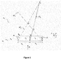
- Figure 1 illustrates the cross-section view, in a XZ plane of a double-material structure 10 according to an embodiment of the present disclosure.
- Such a double-material structure 10, in cross-section view, corresponds to a combination of two different blocks of materials, referenced 12 and 13.
- Such blocks 12, 13 may have a shape of cuboid, for example in the 3D XYZ space, or a shape of semicircular ring.
- Their cross-section is rectangular (as illustrated in figure 1 ), but could also be trapezoidal or cuboid-shaped.
- Blocks referenced 12 and 13 respectively have refractive indexes n 2 and n 3 ( n 2 > n 3 ) embedded in a homogeneous dielectric host medium 11 with a refractive index n 1 ⁇ n 3 .
- refractive index n 2 and n 3 embedded in a homogeneous dielectric host medium 11 with a refractive index n 1 ⁇ n 3 .
- Blocks 12 and 13 could also be placed on a dielectric substrate (not illustrated) acting as a support layer.
- Block 12 has a width W 1 and a height H, while block 13 has a width W 2 and the same height H.
- base angle ⁇ 90°.
- some prismatic structures with arbitrary base angles
- Variation of the base angle value provides additional degree of freedom in the control of the NJ beam radiation.
- the double-material structure 10 once it receives an incident light or electromagnetic wave 14, generates several nanojets beams (the three nanojets beams NJ1, NJ2 and NJ3 generated respectively by edges of the double-material structure 10) that can intersect in different hot spots or focused points or locations referenced as points A, B and C.
- the materials and size of the constitutive parts 11, 12 and 13 can be optimized in order to manage the position of NJ hot spots, intensity, direction and angle of deviation of NJ beams.
- the beam-forming phenomenon appears on an edge between two materials of different refractive indexes, and is associated solely with this edge.
- the ratio of refractive indexes between both materials contributes to controlling an elevation angle of the generated nanojet beam, which is an angular position of a projection of the NJ beam in the vertical xz plane.
- the point of intersection of two equal NJ beams radiated from the opposite sides of the element determines the focal length of the NJ structure.
- the focal length of the NJ structure can be characterized as the function of the size (width) and index ratio of the media inside and outside the structure. The total radiated NJ beam will be directed along the symmetry axis of the system.
- the NJ beam radiation angle at the third edge, between block 13 and host medium 11, corresponds to: ⁇ B 3 ⁇ 90 ° ⁇ ⁇ TIR 3 2 .
- ⁇ TIR 3 sin ⁇ 1 n 1 n 3 .
- the three nanojet beams generated at the boundaries between the materials of different refractive indexes of optical device 10 may partially or totally combine, to produce a total focused beam, which corresponds to the interference pattern caused by the three primary nanojet beams associated with the three edges of device 10.
- the point A of first (NJ1) and second (NJ2) NJs' intersection has the coordinates ( W A , H A ), where: W A ⁇ tan ⁇ B 2 ⁇ H A , H A ⁇ W 1 tan ⁇ B 1 + tan ⁇ B 2 .
- NJ1 and third (NJ3) NJs will intersect at a point B with the coordinates ( W B , H B ), where: W B ⁇ tan ⁇ B 3 ⁇ H B ⁇ W 2 , H B ⁇ W 1 + W 2 tan ⁇ B 1 + tan ⁇ B 3 .
- color components such as the blue, green and red components
- figure 3 presents the power density distribution in xz-plane with n 3 > n 1 n 2 . More precisely, in figure 3 , the height H of the structure is chosen such as H ⁇ H B i.e. the focus point B is close to the surface of the structure.
- the spectral-dependent NJ beam deflection takes place if H ⁇ H B and focal point B for the NJs related to the external boundaries of the structure (NJ1 and NJ3) is close to the surface of structure or within the structure. Playing with the materials of the layers, we can change power density distribution for different colors.
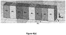
- First array ( figure 4(a) ) corresponds to the periodic alternation of the double-material structures separated by the blocks with refractive index n 1 (in our numerical simulations n 1 is the refractive index of the host medium).
- W 3 is the width of this block (i.e. the block having a material with a refractive index equal to n 1 ).
- second array ( figure 4(b) ) medium with refractive index n 1 separate the blocks with the same refractive indexes.
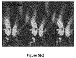
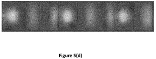
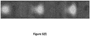
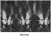
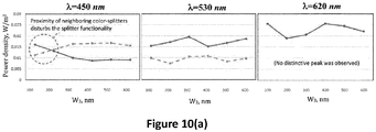
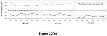
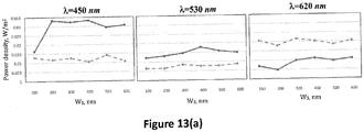
- Figures 5(a) -(f) and figures 6(a) -(f) illustrate power density distribution in the xz-and xy-planes at wavelengths corresponding to the blue, green and red colors for two arrays of double-material dielectric structures with n 3 > n 1 n 2 .
- Each array contains three double-material structures.
- W 3 600 nm.
- W 3 the neighbouring NJs will affect each other just slightly.
- the intensity of the NJ for blue color is higher and distance between the spots for green and red colors is bigger. So, second arrangement is preferable for color splitter application.
- left part (X ⁇ 0) is the part with higher refractive index n 2 ; for the array presented in figure 4(b) (medium with refractive index n1 separate the blocks with the same refractive indexes), left part is the part with lower refractive index n 3 .
- n 2 refractive index
- left part is the part with lower refractive index n 3 .
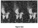
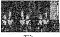
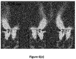
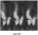
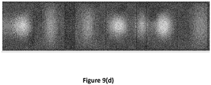
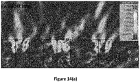
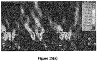
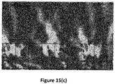
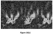
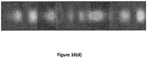
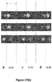
- FIGS 17(a) and 17(b) illustrate the splitting effect of the color splitter microstructures from figures 5(a) -(f) and figures 6(a) -(f).
- the color splitting result of this splitter structure as "blue separation”.
- red separation the color splitting result of this splitter structure
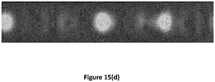
- Figures 17(a) presents a blue separation, as the result of a color splitter design demonstrated in figures 5(a) -(f).
- Figures 17(b) presents a red separation, as the result of a color splitter design demonstrated in figures 7(a) -(f).
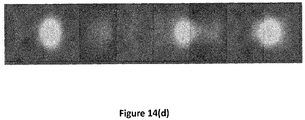
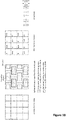
- Figure 18 presents an embodiment showing the 2D arrangement of the splitter elements on top of the regular 2D grid of the image sensor pixels, together with a suggested demosaicing function.
- FIG. 17(a) and 17(b) This embodiment uses the two types of color splitter structures shown figures 17(a) and 17(b) , one tailored for the "blue separation” and the other one tailored for the “red separation” functionality.
- Figure 18 also illustrates the light components received by each pixel on the image sensor together with a suggested demosaicing function.
- Figure 19 presents an embodiment where a color splitter structure as previously presented partially covers at least two pixels.
- each pixel (between pixel 1 and pixel 2) record a different value, for different colors.
- a conventional color filter is added at the top of the photosensitive material in order to filter residual electromagnetic waves.
- Figure 20 provides a cross-section view of a double-material structure with nonvertical edges.
- the NJ beam radiation angle ⁇ Bj can be determined using the approximate formula (08): ⁇ Bj ⁇ 90 ° ⁇ ⁇ ′ TIRj 2 .
- ⁇ ' TIRj are the critical angles of refraction from the nonvertical edges.
- the NJ beam radiation angle can be estimated as: ⁇ Bj ⁇ 90 ° ⁇ ⁇ TIRj + ⁇ j 2 .
- the change of the base angle will change the direction of the NJs and so it affects the crossing points of the nanojet and the color splitting effect.
- the design rule for a color splitter with non-vertical base angle is to calculate the new NJ deviation angles, and the calculate the height H B in which the crossing of the NJs happen and then choose H equal to H B to acheive the color splitting effect.
Landscapes
- Physics & Mathematics (AREA)
- General Physics & Mathematics (AREA)
- Spectroscopy & Molecular Physics (AREA)
- Power Engineering (AREA)
- Engineering & Computer Science (AREA)
- Optics & Photonics (AREA)
- Condensed Matter Physics & Semiconductors (AREA)
- Electromagnetism (AREA)
- Computer Hardware Design (AREA)
- Microelectronics & Electronic Packaging (AREA)
- Spectrometry And Color Measurement (AREA)
- Color Television Image Signal Generators (AREA)
- Solid State Image Pick-Up Elements (AREA)
Priority Applications (7)
| Application Number | Priority Date | Filing Date | Title |
|---|---|---|---|
| EP18305265.3A EP3540499A1 (fr) | 2018-03-13 | 2018-03-13 | Capteur d'images comprenant un séparateur de couleur ayant deux indices de réfraction différents |
| US16/980,326 US11604363B2 (en) | 2018-03-13 | 2019-03-08 | Image sensor comprising a color splitter with two different refractive indexes |
| PCT/EP2019/055905 WO2019175062A1 (fr) | 2018-03-13 | 2019-03-08 | Capteur d'image comprenant un diviseur de couleur à deux indices de réfraction différents |
| RU2020132589A RU2020132589A (ru) | 2018-03-13 | 2019-03-08 | Датчик изображения, содержащий разделитель цветов с двумя различными показателями преломления |
| CN201980029966.9A CN112219153B (zh) | 2018-03-13 | 2019-03-08 | 包括具有两种不同折射率的颜色分离器的图像传感器 |
| EP19708560.8A EP3765893A1 (fr) | 2018-03-13 | 2019-03-08 | Capteur d'image comprenant un diviseur de couleur à deux indices de réfraction différents |
| JP2020548739A JP7339271B2 (ja) | 2018-03-13 | 2019-03-08 | 2つの異なる屈折率を有する色スプリッタを含む画像センサ |
Applications Claiming Priority (1)
| Application Number | Priority Date | Filing Date | Title |
|---|---|---|---|
| EP18305265.3A EP3540499A1 (fr) | 2018-03-13 | 2018-03-13 | Capteur d'images comprenant un séparateur de couleur ayant deux indices de réfraction différents |
Publications (1)
| Publication Number | Publication Date |
|---|---|
| EP3540499A1 true EP3540499A1 (fr) | 2019-09-18 |
Family
ID=62631034
Family Applications (2)
| Application Number | Title | Priority Date | Filing Date |
|---|---|---|---|
| EP18305265.3A Withdrawn EP3540499A1 (fr) | 2018-03-13 | 2018-03-13 | Capteur d'images comprenant un séparateur de couleur ayant deux indices de réfraction différents |
| EP19708560.8A Pending EP3765893A1 (fr) | 2018-03-13 | 2019-03-08 | Capteur d'image comprenant un diviseur de couleur à deux indices de réfraction différents |
Family Applications After (1)
| Application Number | Title | Priority Date | Filing Date |
|---|---|---|---|
| EP19708560.8A Pending EP3765893A1 (fr) | 2018-03-13 | 2019-03-08 | Capteur d'image comprenant un diviseur de couleur à deux indices de réfraction différents |
Country Status (6)
| Country | Link |
|---|---|
| US (1) | US11604363B2 (fr) |
| EP (2) | EP3540499A1 (fr) |
| JP (1) | JP7339271B2 (fr) |
| CN (1) | CN112219153B (fr) |
| RU (1) | RU2020132589A (fr) |
| WO (1) | WO2019175062A1 (fr) |
Cited By (3)
| Publication number | Priority date | Publication date | Assignee | Title |
|---|---|---|---|---|
| US11573356B2 (en) | 2018-03-13 | 2023-02-07 | Interdigital Ce Patent Holdings | Diffraction grating comprising double-materials structures |
| US11604363B2 (en) | 2018-03-13 | 2023-03-14 | Interdigital Ce Patent Holdings | Image sensor comprising a color splitter with two different refractive indexes |
| US11972508B2 (en) | 2018-07-02 | 2024-04-30 | Interdigital Ce Patent Holdings, Sas | Image sensor comprising a color splitter with two different refractive indexes, and different height |
Families Citing this family (2)
| Publication number | Priority date | Publication date | Assignee | Title |
|---|---|---|---|---|
| EP3671310A1 (fr) * | 2018-12-18 | 2020-06-24 | Thomson Licensing | Appareil de manipulation optique pour piéger ou déplacer des micro ou des nanoparticules |
| WO2022023170A1 (fr) | 2020-07-30 | 2022-02-03 | Interdigital Ce Patent Holdings, Sas | Système de séparateur de couleur |
Citations (3)
| Publication number | Priority date | Publication date | Assignee | Title |
|---|---|---|---|---|
| US20130099343A1 (en) * | 2010-07-02 | 2013-04-25 | Panasonic Corporation | Solid-state imaging device |
| EP3223062A1 (fr) * | 2016-03-24 | 2017-09-27 | Thomson Licensing | Dispositif de formation d'au moins un faisceau focalisé dans la zone proche, à partir des ondes électromagnétiques incidentes |
| EP3223063A1 (fr) | 2016-03-24 | 2017-09-27 | Thomson Licensing | Dispositif de formation d'un motif d'intensité de champ dans la zone proche, à partir des ondes électromagnétiques incidentes |
Family Cites Families (71)
| Publication number | Priority date | Publication date | Assignee | Title |
|---|---|---|---|---|
| US3718383A (en) | 1971-04-19 | 1973-02-27 | Eastman Kodak Co | Plastic optical element having refractive index gradient |
| JP3891628B2 (ja) | 1997-02-04 | 2007-03-14 | オリンパス株式会社 | 照明光学系及びこれを備えた内視鏡システム |
| EP1406098A4 (fr) | 2001-07-10 | 2005-09-21 | Sumitomo Electric Industries | Dispositif a reseau de diffraction de guide d'ondes optiques et procede de fabrication correspondant |
| WO2003025635A1 (fr) | 2001-09-19 | 2003-03-27 | Technion Research & Development Foundation Ltd. | Reseau dielectrique sub-$g(l) a variation spatiale et ses applications |
| US7573638B2 (en) | 2002-09-19 | 2009-08-11 | Sumitomo Electric Industries, Ltd. | Diffractive optical element and method of its formation |
| TWI319124B (en) | 2003-02-27 | 2010-01-01 | Asml Netherlands Bv | Stationary and dynamic radial transverse electric polarizer for high numerical aperture systems |
| FI115169B (fi) | 2003-05-13 | 2005-03-15 | Nokia Corp | Menetelmä ja optinen järjestelmä valon kytkemiseksi aaltojohteeseen |
| US7456384B2 (en) * | 2004-12-10 | 2008-11-25 | Sony Corporation | Method and apparatus for acquiring physical information, method for manufacturing semiconductor device including array of plurality of unit components for detecting physical quantity distribution, light-receiving device and manufacturing method therefor, and solid-state imaging device and manufacturing method therefor |
| WO2007031991A2 (fr) | 2005-09-14 | 2007-03-22 | Mirage Innovations Ltd. | Dispositif optique a diffraction et systeme |
| JP4893200B2 (ja) | 2006-09-28 | 2012-03-07 | ブラザー工業株式会社 | 光束転送用の光学系、及び、これを用いた網膜走査型ディスプレイ |
| US8212859B2 (en) | 2006-10-13 | 2012-07-03 | Apple Inc. | Peripheral treatment for head-mounted displays |
| US7394535B1 (en) | 2007-03-20 | 2008-07-01 | Tokyo Electron Limited | Optical metrology using a photonic nanojet |
| WO2009083977A2 (fr) | 2008-01-02 | 2009-07-09 | Mirage Innovations Ltd. | Dispositif optique pour relayer une lumière polychrome |
| WO2010045366A1 (fr) | 2008-10-17 | 2010-04-22 | The Arizona Board Of Regents On Behalf Of The University Of Arizona | Appareil et procédé de génération de faisceaux pratiquement non diffractants à partir de fibres optiques multimodales |
| EP2196729A1 (fr) | 2008-12-12 | 2010-06-16 | BAE Systems PLC | Améliorations de guides d'ondes ou relatives à ceux-ci |
| JP6007830B2 (ja) | 2012-03-26 | 2016-10-12 | 旭硝子株式会社 | 透過型回折素子 |
| US8989535B2 (en) | 2012-06-04 | 2015-03-24 | Microsoft Technology Licensing, Llc | Multiple waveguide imaging structure |
| US9140602B2 (en) | 2012-08-11 | 2015-09-22 | The Board Of Trustees Of The Leland Stanford Junior University | Nanophotonic light-field sensor |
| US8885997B2 (en) | 2012-08-31 | 2014-11-11 | Microsoft Corporation | NED polarization system for wavelength pass-through |
| JP6094832B2 (ja) | 2012-09-03 | 2017-03-15 | パナソニックIpマネジメント株式会社 | 固体撮像素子および撮像装置 |
| FI125270B (en) | 2012-09-20 | 2015-08-14 | Teknologian Tutkimuskeskus Vtt Oy | Optical device with diffractive grating |
| JP6011826B2 (ja) | 2012-10-18 | 2016-10-19 | パナソニックIpマネジメント株式会社 | 固体撮像素子 |
| WO2014176277A1 (fr) | 2013-04-22 | 2014-10-30 | Cornell University | Dispositifs optiques athermiques à base de structures composites |
| US10371898B2 (en) | 2013-09-05 | 2019-08-06 | Southern Methodist University | Enhanced coupling strength grating having a cover layer |
| KR102276432B1 (ko) * | 2014-04-07 | 2021-07-09 | 삼성전자주식회사 | 색분리 소자 및 상기 색분리 소자를 포함하는 이미지 센서 |
| KR102159166B1 (ko) | 2014-05-09 | 2020-09-23 | 삼성전자주식회사 | 색분리 소자 및 상기 색분리 소자를 포함하는 이미지 센서 |
| KR102261855B1 (ko) | 2014-06-13 | 2021-06-07 | 삼성전자주식회사 | 색분리 소자를 포함하는 적층형 이미지 센서 및 상기 이미지 센서를 포함하는 촬상 장치 |
| US9726794B2 (en) | 2014-06-13 | 2017-08-08 | The Regents Of The University Of California | High index contrast grating structure for light manipulation and related method |
| GB2529003B (en) | 2014-08-03 | 2020-08-26 | Wave Optics Ltd | Optical device |
| KR20160023158A (ko) | 2014-08-21 | 2016-03-03 | 삼성전자주식회사 | 광 이용 효율이 향상된 이미지 센서 및 그 제조방법 |
| KR102323204B1 (ko) | 2014-08-22 | 2021-11-08 | 삼성전자주식회사 | 선명한 색 구현이 가능한 이미지 센서 및 그 제조방법 |
| US20160064172A1 (en) | 2014-09-02 | 2016-03-03 | Delta Systems, Inc. | Plunger switch assembly and method of operation |
| KR102307458B1 (ko) | 2014-10-20 | 2021-09-30 | 삼성전자주식회사 | 색분리 소자 및 그 제조 방법 및 이를 포함하는 이미지 센서 |
| US9513480B2 (en) | 2015-02-09 | 2016-12-06 | Microsoft Technology Licensing, Llc | Waveguide |
| EP3113478A1 (fr) | 2015-06-30 | 2017-01-04 | Thomson Licensing | Caméra à fonction plenoptique par fovéation |
| US10431624B2 (en) | 2015-07-08 | 2019-10-01 | Samsung Electronics Co., Ltd. | Method of manufacturing image sensor including nanostructure color filter |
| US10866360B2 (en) | 2015-08-19 | 2020-12-15 | President And Fellows Of Harvard College | Broadband multifunctional efficient meta-gratings based on dielectric waveguide phase shifters |
| US20180252850A1 (en) | 2015-08-20 | 2018-09-06 | Hoya Lens Thailand Ltd. | Optical device |
| KR102501643B1 (ko) | 2015-09-24 | 2023-02-20 | 삼성전자주식회사 | 고굴절률 광학 기능층을 포함하는 광학 장치 및 상기 광학 장치의 제조 방법 |
| KR102519178B1 (ko) * | 2015-09-25 | 2023-04-06 | 삼성전자주식회사 | 색분리 소자를 포함하는 이미지 센서 및 이를 포함하는 촬상 장치 |
| KR102465995B1 (ko) | 2015-09-30 | 2022-11-25 | 삼성전자주식회사 | 색분할기 구조와 그 제조방법, 색분할기 구조를 포함하는 이미지센서 및 이미지센서를 포함하는 광학장치 |
| KR102409389B1 (ko) | 2015-10-06 | 2022-06-15 | 삼성전자주식회사 | 색분리 소자를 포함하는 이미지 센서 |
| KR102556008B1 (ko) * | 2015-10-06 | 2023-07-17 | 삼성전자주식회사 | 이미지 센서의 컬러 스플리터 |
| KR102561097B1 (ko) | 2015-12-22 | 2023-07-28 | 삼성전자주식회사 | 색분리 소자 어레이, 이를 포함한 이미지 센서 및 전자 장치 |
| US9927614B2 (en) | 2015-12-29 | 2018-03-27 | Microsoft Technology Licensing, Llc | Augmented reality display system with variable focus |
| US9720237B1 (en) | 2016-01-27 | 2017-08-01 | Microsoft Technology Licensing, Llc. | Mixed environment display device and waveguide cross-coupling suppressors |
| US9891436B2 (en) | 2016-02-11 | 2018-02-13 | Microsoft Technology Licensing, Llc | Waveguide-based displays with anti-reflective and highly-reflective coating |
| US9791703B1 (en) | 2016-04-13 | 2017-10-17 | Microsoft Technology Licensing, Llc | Waveguides with extended field of view |
| US10197804B2 (en) | 2016-04-25 | 2019-02-05 | Microsoft Technology Licensing, Llc | Refractive coating for diffractive optical elements |
| US10061124B2 (en) | 2016-04-29 | 2018-08-28 | Microsoft Technology Licensing, Llc | Robust architecture for large field of view components |
| EP3240046A1 (fr) | 2016-04-29 | 2017-11-01 | BASF Coatings GmbH | Collecteur de lumière solaire |
| WO2018067074A1 (fr) | 2016-10-05 | 2018-04-12 | Agency For Science, Technology And Research | Élément optique diffractif et procédé de formation de celui-ci |
| EP3312646A1 (fr) | 2016-10-21 | 2018-04-25 | Thomson Licensing | Dispositif et procédé de protection d'au moins un objet à l'échelle de la sous-longueur d'onde à partir d'une onde électromagnétique incidente |
| EP3312674A1 (fr) | 2016-10-21 | 2018-04-25 | Thomson Licensing | Dispositif de photolithographie pour générer un motif sur un substrat de résine photosensible |
| EP3312660A1 (fr) | 2016-10-21 | 2018-04-25 | Thomson Licensing | Dispositif de formation d'au moins un faisceau incliné focalisé dans la zone proche à partir des ondes électromagnétiques incidentes |
| JP6960994B2 (ja) | 2016-10-26 | 2021-11-05 | マジック リープ, インコーポレイテッドMagic Leap, Inc. | 拡張現実システムのための外部結合回折格子 |
| US10175564B2 (en) | 2016-12-01 | 2019-01-08 | Magic Leap, Inc. | Projector with scanning array light engine |
| US11513350B2 (en) | 2016-12-02 | 2022-11-29 | Digilens Inc. | Waveguide device with uniform output illumination |
| CN106772734A (zh) | 2017-01-03 | 2017-05-31 | 中国科学院上海光学精密机械研究所 | 宽带高衍射效率非对称形貌反射型光栅 |
| IL268261B2 (en) | 2017-02-15 | 2024-04-01 | Magic Leap Inc | A projector architecture that incorporates false discovery reduction |
| EP3385219B1 (fr) | 2017-04-07 | 2021-07-14 | InterDigital CE Patent Holdings | Procédé de fabrication d'un dispositif de formation d'au moins un faisceau focalisé dans une zone proche |
| US10534115B1 (en) | 2017-09-22 | 2020-01-14 | Facebook Technologies, Llc | Gray-tone electron-beam lithography |
| AU2018351321B9 (en) | 2017-10-20 | 2023-09-21 | Magic Leap, Inc. | Configuring optical layers in imprint lithography processes |
| EP3499278A1 (fr) | 2017-12-13 | 2019-06-19 | Thomson Licensing | Structure de réseau de diffraction comprenant plusieurs lignes de réseau |
| EP3540499A1 (fr) | 2018-03-13 | 2019-09-18 | Thomson Licensing | Capteur d'images comprenant un séparateur de couleur ayant deux indices de réfraction différents |
| EP3540479A1 (fr) | 2018-03-13 | 2019-09-18 | Thomson Licensing | Réseau de diffraction comprenant des structures à double matériau |
| EP3588150A1 (fr) | 2018-06-29 | 2020-01-01 | Thomson Licensing | Dispositif optique comprenant des guide d'ondes à plusieurs couches |
| EP3591700A1 (fr) | 2018-07-02 | 2020-01-08 | Thomson Licensing | Capteur d'images comprenant un séparateur de couleur ayant deux indices de réfraction différents et une hauteur différente |
| EP3671322A1 (fr) | 2018-12-18 | 2020-06-24 | Thomson Licensing | Dispositif de formation d'une onde électromagnétique sortant d'une onde électromagnétique incidente |
| EP3671293A1 (fr) | 2018-12-21 | 2020-06-24 | Thomson Licensing | Dispositif optique comprenant au moins un réseau de diffraction doté d'un pas de réseau supérieur à la longueur d'onde |
| EP4031927A1 (fr) | 2019-09-19 | 2022-07-27 | InterDigital CE Patent Holdings | Dispositif optique pour coupler un champ de vision élevé de lumière incidente |
-
2018
- 2018-03-13 EP EP18305265.3A patent/EP3540499A1/fr not_active Withdrawn
-
2019
- 2019-03-08 US US16/980,326 patent/US11604363B2/en active Active
- 2019-03-08 EP EP19708560.8A patent/EP3765893A1/fr active Pending
- 2019-03-08 WO PCT/EP2019/055905 patent/WO2019175062A1/fr unknown
- 2019-03-08 JP JP2020548739A patent/JP7339271B2/ja active Active
- 2019-03-08 CN CN201980029966.9A patent/CN112219153B/zh active Active
- 2019-03-08 RU RU2020132589A patent/RU2020132589A/ru unknown
Patent Citations (3)
| Publication number | Priority date | Publication date | Assignee | Title |
|---|---|---|---|---|
| US20130099343A1 (en) * | 2010-07-02 | 2013-04-25 | Panasonic Corporation | Solid-state imaging device |
| EP3223062A1 (fr) * | 2016-03-24 | 2017-09-27 | Thomson Licensing | Dispositif de formation d'au moins un faisceau focalisé dans la zone proche, à partir des ondes électromagnétiques incidentes |
| EP3223063A1 (fr) | 2016-03-24 | 2017-09-27 | Thomson Licensing | Dispositif de formation d'un motif d'intensité de champ dans la zone proche, à partir des ondes électromagnétiques incidentes |
Non-Patent Citations (1)
| Title |
|---|
| VICTOR V. KOTLYAR ET AL: "Photonic nanojets generated using square-profile microsteps", APPLIED OPTICS, vol. 53, no. 24, 20 August 2014 (2014-08-20), WASHINGTON, DC; US, pages 5322, XP055357764, ISSN: 0003-6935, DOI: 10.1364/AO.53.005322 * |
Cited By (3)
| Publication number | Priority date | Publication date | Assignee | Title |
|---|---|---|---|---|
| US11573356B2 (en) | 2018-03-13 | 2023-02-07 | Interdigital Ce Patent Holdings | Diffraction grating comprising double-materials structures |
| US11604363B2 (en) | 2018-03-13 | 2023-03-14 | Interdigital Ce Patent Holdings | Image sensor comprising a color splitter with two different refractive indexes |
| US11972508B2 (en) | 2018-07-02 | 2024-04-30 | Interdigital Ce Patent Holdings, Sas | Image sensor comprising a color splitter with two different refractive indexes, and different height |
Also Published As
| Publication number | Publication date |
|---|---|
| WO2019175062A1 (fr) | 2019-09-19 |
| EP3765893A1 (fr) | 2021-01-20 |
| US11604363B2 (en) | 2023-03-14 |
| CN112219153A (zh) | 2021-01-12 |
| JP7339271B2 (ja) | 2023-09-05 |
| JP2021517765A (ja) | 2021-07-26 |
| CN112219153B (zh) | 2023-07-18 |
| RU2020132589A (ru) | 2022-04-04 |
| US20210041709A1 (en) | 2021-02-11 |
Similar Documents
| Publication | Publication Date | Title |
|---|---|---|
| US11604363B2 (en) | Image sensor comprising a color splitter with two different refractive indexes | |
| JP4455677B2 (ja) | 撮像用光検出装置 | |
| JP4264465B2 (ja) | 撮像用光検出装置 | |
| JP7396898B2 (ja) | 赤外マルチスペクトル撮像用の装置及び方法 | |
| US10393576B2 (en) | Image sensor including color filter isolation layer and method of manufacturing the same | |
| US9853073B2 (en) | Image sensor for producing vivid colors and method of manufacturing the same | |
| CN105280655B (zh) | 光电转换装置与成像系统 | |
| US9099370B2 (en) | Solid-state imaging element and imaging device | |
| EP2037298A1 (fr) | Élément optique et dispositif optique le comprenant | |
| US11972508B2 (en) | Image sensor comprising a color splitter with two different refractive indexes, and different height | |
| KR102395775B1 (ko) | 컬러 필터를 포함하는 이미지 센서 및 상기 이미지 센서의 제조 방법 | |
| JP5188107B2 (ja) | アレイ型受光素子 | |
| EP3513229A1 (fr) | Ensemble lentille de métasurface pour séparation chromatique | |
| US11158661B2 (en) | Image sensor with micro-structured color filter | |
| US10276612B2 (en) | Photoelectric conversion apparatus and image pickup system | |
| WO2022023170A1 (fr) | Système de séparateur de couleur | |
| JP2007079325A (ja) | マイクロレンズアレイ | |
| CN104166228B (zh) | 数字全像显微镜 | |
| JP2017167115A (ja) | 光検出装置 | |
| CN105575985A (zh) | 半导体光学感测器 | |
| KR20110065178A (ko) | 이미지 센서의 마이크로 렌즈 및 이미지 센서의 마이크로 렌즈 제조 방법 |
Legal Events
| Date | Code | Title | Description |
|---|---|---|---|
| PUAI | Public reference made under article 153(3) epc to a published international application that has entered the european phase |
Free format text: ORIGINAL CODE: 0009012 |
|
| AK | Designated contracting states |
Kind code of ref document: A1 Designated state(s): AL AT BE BG CH CY CZ DE DK EE ES FI FR GB GR HR HU IE IS IT LI LT LU LV MC MK MT NL NO PL PT RO RS SE SI SK SM TR |
|
| AX | Request for extension of the european patent |
Extension state: BA ME |
|
| RAP1 | Party data changed (applicant data changed or rights of an application transferred) |
Owner name: INTERDIGITAL CE PATENT HOLDINGS |
|
| STAA | Information on the status of an ep patent application or granted ep patent |
Free format text: STATUS: THE APPLICATION IS DEEMED TO BE WITHDRAWN |
|
| 18D | Application deemed to be withdrawn |
Effective date: 20200603 |