EP3540499A1 - Image sensor comprising a color splitter with two different refractive indexes - Google Patents
Image sensor comprising a color splitter with two different refractive indexes Download PDFInfo
- Publication number
- EP3540499A1 EP3540499A1 EP18305265.3A EP18305265A EP3540499A1 EP 3540499 A1 EP3540499 A1 EP 3540499A1 EP 18305265 A EP18305265 A EP 18305265A EP 3540499 A1 EP3540499 A1 EP 3540499A1
- Authority
- EP
- European Patent Office
- Prior art keywords
- image sensor
- color splitter
- wavelength
- pixels
- splitter structure
- Prior art date
- Legal status (The legal status is an assumption and is not a legal conclusion. Google has not performed a legal analysis and makes no representation as to the accuracy of the status listed.)
- Withdrawn
Links
- 230000005855 radiation Effects 0.000 claims abstract description 14
- 238000001228 spectrum Methods 0.000 claims abstract description 5
- 239000000463 material Substances 0.000 claims description 52
- 239000011521 glass Substances 0.000 claims description 2
- 239000002861 polymer material Substances 0.000 claims description 2
- 239000003086 colorant Substances 0.000 description 17
- 238000003491 array Methods 0.000 description 12
- 238000000926 separation method Methods 0.000 description 8
- 230000000737 periodic effect Effects 0.000 description 7
- 230000001419 dependent effect Effects 0.000 description 4
- 230000000694 effects Effects 0.000 description 4
- 230000003595 spectral effect Effects 0.000 description 4
- NCGICGYLBXGBGN-UHFFFAOYSA-N 3-morpholin-4-yl-1-oxa-3-azonia-2-azanidacyclopent-3-en-5-imine;hydrochloride Chemical compound Cl.[N-]1OC(=N)C=[N+]1N1CCOCC1 NCGICGYLBXGBGN-UHFFFAOYSA-N 0.000 description 3
- 101100420681 Caenorhabditis elegans tir-1 gene Proteins 0.000 description 3
- 230000003287 optical effect Effects 0.000 description 3
- 238000004088 simulation Methods 0.000 description 3
- 239000003989 dielectric material Substances 0.000 description 2
- 230000014509 gene expression Effects 0.000 description 2
- 238000000034 method Methods 0.000 description 2
- 238000004458 analytical method Methods 0.000 description 1
- 230000015572 biosynthetic process Effects 0.000 description 1
- 239000006185 dispersion Substances 0.000 description 1
- 230000009977 dual effect Effects 0.000 description 1
- 238000005286 illumination Methods 0.000 description 1
- 230000004048 modification Effects 0.000 description 1
- 238000012986 modification Methods 0.000 description 1
- 150000004767 nitrides Chemical class 0.000 description 1
- 239000000758 substrate Substances 0.000 description 1
Images


Classifications
-
- G—PHYSICS
- G02—OPTICS
- G02B—OPTICAL ELEMENTS, SYSTEMS OR APPARATUS
- G02B27/00—Optical systems or apparatus not provided for by any of the groups G02B1/00 - G02B26/00, G02B30/00
- G02B27/10—Beam splitting or combining systems
- G02B27/1006—Beam splitting or combining systems for splitting or combining different wavelengths
- G02B27/1013—Beam splitting or combining systems for splitting or combining different wavelengths for colour or multispectral image sensors, e.g. splitting an image into monochromatic image components on respective sensors
-
- H—ELECTRICITY
- H01—ELECTRIC ELEMENTS
- H01L—SEMICONDUCTOR DEVICES NOT COVERED BY CLASS H10
- H01L27/00—Devices consisting of a plurality of semiconductor or other solid-state components formed in or on a common substrate
- H01L27/14—Devices consisting of a plurality of semiconductor or other solid-state components formed in or on a common substrate including semiconductor components sensitive to infrared radiation, light, electromagnetic radiation of shorter wavelength or corpuscular radiation and specially adapted either for the conversion of the energy of such radiation into electrical energy or for the control of electrical energy by such radiation
- H01L27/144—Devices controlled by radiation
- H01L27/146—Imager structures
- H01L27/14601—Structural or functional details thereof
- H01L27/14625—Optical elements or arrangements associated with the device
-
- G—PHYSICS
- G01—MEASURING; TESTING
- G01J—MEASUREMENT OF INTENSITY, VELOCITY, SPECTRAL CONTENT, POLARISATION, PHASE OR PULSE CHARACTERISTICS OF INFRARED, VISIBLE OR ULTRAVIOLET LIGHT; COLORIMETRY; RADIATION PYROMETRY
- G01J3/00—Spectrometry; Spectrophotometry; Monochromators; Measuring colours
- G01J3/46—Measurement of colour; Colour measuring devices, e.g. colorimeters
- G01J3/50—Measurement of colour; Colour measuring devices, e.g. colorimeters using electric radiation detectors
- G01J3/51—Measurement of colour; Colour measuring devices, e.g. colorimeters using electric radiation detectors using colour filters
-
- G—PHYSICS
- G02—OPTICS
- G02B—OPTICAL ELEMENTS, SYSTEMS OR APPARATUS
- G02B27/00—Optical systems or apparatus not provided for by any of the groups G02B1/00 - G02B26/00, G02B30/00
- G02B27/56—Optics using evanescent waves, i.e. inhomogeneous waves
-
- H—ELECTRICITY
- H01—ELECTRIC ELEMENTS
- H01L—SEMICONDUCTOR DEVICES NOT COVERED BY CLASS H10
- H01L27/00—Devices consisting of a plurality of semiconductor or other solid-state components formed in or on a common substrate
- H01L27/14—Devices consisting of a plurality of semiconductor or other solid-state components formed in or on a common substrate including semiconductor components sensitive to infrared radiation, light, electromagnetic radiation of shorter wavelength or corpuscular radiation and specially adapted either for the conversion of the energy of such radiation into electrical energy or for the control of electrical energy by such radiation
- H01L27/144—Devices controlled by radiation
- H01L27/146—Imager structures
- H01L27/14601—Structural or functional details thereof
- H01L27/1462—Coatings
- H01L27/14621—Colour filter arrangements
Definitions
- the present disclosure relates to the field of optics and photonics, and more specifically to optical devices used in image sensors.
- an image sensor In order to acquire color components during the acquisition of an image, usually an image sensor can either use a Bayer filter (which is a way of discretizing the color space, that requires the execution of a kind of interpolation later for generating a color image), or a Fovea sensor (being able to record three color components per pixel via a stack of color sensors, i.e. the color sensors are piled up on each other's).
- a Bayer filter which is a way of discretizing the color space, that requires the execution of a kind of interpolation later for generating a color image
- a Fovea sensor being able to record three color components per pixel via a stack of color sensors, i.e. the color sensors are piled up on each other's.
- references in the specification to "one embodiment”, “an embodiment”, “an example embodiment”, indicate that the embodiment described may include a particular feature, structure, or characteristic, but every embodiment may not necessarily include the particular feature, structure, or characteristic. Moreover, such phrases are not necessarily referring to the same embodiment. Further, when a particular feature, structure, or characteristic is described in connection with an embodiment, it is submitted that it is within the knowledge of one skilled in the art to affect such feature, structure, or characteristic in connection with other embodiments whether or not explicitly described.
- an image sensor comprising pixels for acquiring color information from incoming visible light, wherein said image sensor being associated with a three-dimensional cartesian coordinate system defined by axis x, y and z, wherein the z-axis being normal to said image sensor, said image sensor comprising at least two pixels being partially covered by a color splitter structure comprising a first part and a second part, that are positioned side by side along said x-axis, and each of said first and second parts being adjacent to a dielectric part along said x-axis, each of said dielectric part having a first refractive index n 1 , said first part having a second refractive index n 2 , and said second part having a third refractive index n 3 , wherein n 1 ⁇ n 3 ⁇ n 2 , and wherein according to a cross section with a plane xz, the first part of said color splitter structure has a first width W 1 along the x-axis, a height H along
- the image sensor has parameters with n 3 > n 1 n 2 and a width W of said color splitter structure, equal to W 1 + W 2 , is greater than 390 nm, and said one of said at least two pixels that records light associated with a first wavelength ⁇ 1 is located at the normal of said first part of said color splitter structure, in the case said first wavelength ⁇ 1 is high in a range of visible light.
- the image sensor has parameters with n 3 > n 1 n 2 and a width W of said color splitter structure, equal to W 1 + W 2 , is greater than 390 nm, and said one of said at least two pixels that records light associated with a first wavelength ⁇ 1 is located at the normal of said second part of said color splitter structure, in the case said first wavelength ⁇ 1 is small in a range of visible light.
- the image sensor has parameters with n 3 ⁇ n 1 n 2 and a width W of said color splitter structure, equal to W 1 + W 2 , is greater than 390 nm, and said one of said at least two pixels that records light associated with a first wavelength ⁇ 1 is located at the normal of said second part of said color splitter structure, in the case said first wavelength ⁇ 1 is high in a range of visible light.
- the image sensor has parameters with n 3 ⁇ n 1 n 2 and a width W of said color splitter structure, equal to W 1 + W 2 , is greater than 390 nm, and said one of said at least two pixels that records light associated with a first wavelength ⁇ 1 is located at the normal of said first part of said color splitter structure, in the case said first wavelength ⁇ 1 is small in a range of visible light.
- said visible light comprises electromagnetic waves having wavelengths that go from 390 nm to 700 nm.
- said wavelength ⁇ 1 belongs to range [390nm, 450 nm].
- said wavelength ⁇ 1 belongs to range [620 nm, 700nm].
- said first width W 1 and said second width W 2 are equal to each other.
- each pair of pixels is partially covered by a structure identical to said color splitter structure.
- each pair of pixels is partially covered by a structure that is alternatively either a structure identical to said color splitter structure, or a structure comprising first and second parts which are inverted compared to said color splitter structure.
- each successive structure is separated by an identical dielectric part having a width, along the x-axis, equal to W 3 , and wherein the value of W 3 is comprised between 250 nm and 600 nm.
- each first and second part, and said dielectric part are made of a material that belongs to the group comprising:
- At least one pixel of said at least two pixels further comprises conventional color filter positioned between said color splitter structure and photosensitive materials associated with each of said at least two pixels.
- said height H is around ⁇ 5% of the value H B .
- said radiation angles of said first and said third beams ⁇ B 1 and ⁇ B 3 are equal to 90 ° ⁇ ⁇ TIRj + ⁇ j 2 , where angles ⁇ j , with j equals to 1 or 3, are the base angles for said first and third edges, and ⁇ TIRj , with j equals to 1 or 3, are critical angles of refraction associated with respectively said first and third edges.
- the image sensor is remarkable in that said one of said at least two pixels that records light associated with said first wavelength ⁇ 1 , further receives light associated with said first wavelength from another neighbor color splitter structure.
- the image sensor is remarkable in that said other of said at least two pixels further receives light, having a spectrum in which no or few electromagnetic waves having a wavelength equal to ⁇ 1 are present, from another neighbor color splitter structure.
- the present disclosure relates to a technique for splitting color-bands of an incident visible light by combining two or more dielectric materials with different refractive indexes (the refractive indexes of constitutive parts are higher than the surrounding material) in such a way that all the nanojets (NJ) beams, originating from different edges (associated with different blocks/layers) of the microstructure, recombine and contribute to the formation of a spectral-dependent NJ beam deflection.
- NJ nanojets
- an element or structure that can perform such color splitting or deviating structure is a specific configuration of a more general design of a NJ beam forming element (also called hereafter a double-material structure) which is a combination of at least two dielectric materials with different refractive indexes having a nonsymmetrical or a symmetrical system in a vertical cross-section.
- a NJ beam forming element also called hereafter a double-material structure
- structures having such a topology are referred to as structures based on a combination of different materials.
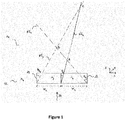
- Figure 1 illustrates the cross-section view, in a XZ plane of a double-material structure 10 according to an embodiment of the present disclosure.
- Such a double-material structure 10, in cross-section view, corresponds to a combination of two different blocks of materials, referenced 12 and 13.
- Such blocks 12, 13 may have a shape of cuboid, for example in the 3D XYZ space, or a shape of semicircular ring.
- Their cross-section is rectangular (as illustrated in figure 1 ), but could also be trapezoidal or cuboid-shaped.
- Blocks referenced 12 and 13 respectively have refractive indexes n 2 and n 3 ( n 2 > n 3 ) embedded in a homogeneous dielectric host medium 11 with a refractive index n 1 ⁇ n 3 .
- refractive index n 2 and n 3 embedded in a homogeneous dielectric host medium 11 with a refractive index n 1 ⁇ n 3 .
- Blocks 12 and 13 could also be placed on a dielectric substrate (not illustrated) acting as a support layer.
- Block 12 has a width W 1 and a height H, while block 13 has a width W 2 and the same height H.
- base angle ⁇ 90°.
- some prismatic structures with arbitrary base angles
- Variation of the base angle value provides additional degree of freedom in the control of the NJ beam radiation.
- the double-material structure 10 once it receives an incident light or electromagnetic wave 14, generates several nanojets beams (the three nanojets beams NJ1, NJ2 and NJ3 generated respectively by edges of the double-material structure 10) that can intersect in different hot spots or focused points or locations referenced as points A, B and C.
- the materials and size of the constitutive parts 11, 12 and 13 can be optimized in order to manage the position of NJ hot spots, intensity, direction and angle of deviation of NJ beams.
- the beam-forming phenomenon appears on an edge between two materials of different refractive indexes, and is associated solely with this edge.
- the ratio of refractive indexes between both materials contributes to controlling an elevation angle of the generated nanojet beam, which is an angular position of a projection of the NJ beam in the vertical xz plane.
- the point of intersection of two equal NJ beams radiated from the opposite sides of the element determines the focal length of the NJ structure.
- the focal length of the NJ structure can be characterized as the function of the size (width) and index ratio of the media inside and outside the structure. The total radiated NJ beam will be directed along the symmetry axis of the system.
- the NJ beam radiation angle at the third edge, between block 13 and host medium 11, corresponds to: ⁇ B 3 ⁇ 90 ° ⁇ ⁇ TIR 3 2 .
- ⁇ TIR 3 sin ⁇ 1 n 1 n 3 .
- the three nanojet beams generated at the boundaries between the materials of different refractive indexes of optical device 10 may partially or totally combine, to produce a total focused beam, which corresponds to the interference pattern caused by the three primary nanojet beams associated with the three edges of device 10.
- the point A of first (NJ1) and second (NJ2) NJs' intersection has the coordinates ( W A , H A ), where: W A ⁇ tan ⁇ B 2 ⁇ H A , H A ⁇ W 1 tan ⁇ B 1 + tan ⁇ B 2 .
- NJ1 and third (NJ3) NJs will intersect at a point B with the coordinates ( W B , H B ), where: W B ⁇ tan ⁇ B 3 ⁇ H B ⁇ W 2 , H B ⁇ W 1 + W 2 tan ⁇ B 1 + tan ⁇ B 3 .
- color components such as the blue, green and red components
- figure 3 presents the power density distribution in xz-plane with n 3 > n 1 n 2 . More precisely, in figure 3 , the height H of the structure is chosen such as H ⁇ H B i.e. the focus point B is close to the surface of the structure.
- the spectral-dependent NJ beam deflection takes place if H ⁇ H B and focal point B for the NJs related to the external boundaries of the structure (NJ1 and NJ3) is close to the surface of structure or within the structure. Playing with the materials of the layers, we can change power density distribution for different colors.
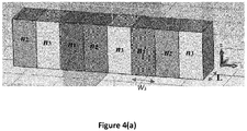
- First array ( figure 4(a) ) corresponds to the periodic alternation of the double-material structures separated by the blocks with refractive index n 1 (in our numerical simulations n 1 is the refractive index of the host medium).
- W 3 is the width of this block (i.e. the block having a material with a refractive index equal to n 1 ).
- second array ( figure 4(b) ) medium with refractive index n 1 separate the blocks with the same refractive indexes.
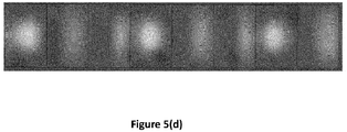
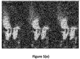
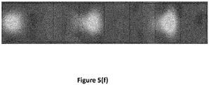
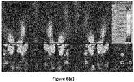
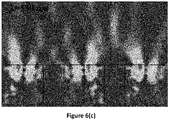
- Figures 5(a) -(f) and figures 6(a) -(f) illustrate power density distribution in the xz-and xy-planes at wavelengths corresponding to the blue, green and red colors for two arrays of double-material dielectric structures with n 3 > n 1 n 2 .
- Each array contains three double-material structures.
- W 3 600 nm.
- W 3 the neighbouring NJs will affect each other just slightly.
- the intensity of the NJ for blue color is higher and distance between the spots for green and red colors is bigger. So, second arrangement is preferable for color splitter application.
- left part (X ⁇ 0) is the part with higher refractive index n 2 ; for the array presented in figure 4(b) (medium with refractive index n1 separate the blocks with the same refractive indexes), left part is the part with lower refractive index n 3 .
- n 2 refractive index
- left part is the part with lower refractive index n 3 .
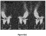
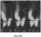
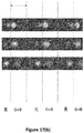
- FIGS 17(a) and 17(b) illustrate the splitting effect of the color splitter microstructures from figures 5(a) -(f) and figures 6(a) -(f).
- the color splitting result of this splitter structure as "blue separation”.
- red separation the color splitting result of this splitter structure
- Figures 17(a) presents a blue separation, as the result of a color splitter design demonstrated in figures 5(a) -(f).
- Figures 17(b) presents a red separation, as the result of a color splitter design demonstrated in figures 7(a) -(f).
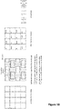
- Figure 18 presents an embodiment showing the 2D arrangement of the splitter elements on top of the regular 2D grid of the image sensor pixels, together with a suggested demosaicing function.
- FIG. 17(a) and 17(b) This embodiment uses the two types of color splitter structures shown figures 17(a) and 17(b) , one tailored for the "blue separation” and the other one tailored for the “red separation” functionality.
- Figure 18 also illustrates the light components received by each pixel on the image sensor together with a suggested demosaicing function.
- Figure 19 presents an embodiment where a color splitter structure as previously presented partially covers at least two pixels.
- each pixel (between pixel 1 and pixel 2) record a different value, for different colors.
- a conventional color filter is added at the top of the photosensitive material in order to filter residual electromagnetic waves.
- Figure 20 provides a cross-section view of a double-material structure with nonvertical edges.
- the NJ beam radiation angle ⁇ Bj can be determined using the approximate formula (08): ⁇ Bj ⁇ 90 ° ⁇ ⁇ ′ TIRj 2 .
- ⁇ ' TIRj are the critical angles of refraction from the nonvertical edges.
- the NJ beam radiation angle can be estimated as: ⁇ Bj ⁇ 90 ° ⁇ ⁇ TIRj + ⁇ j 2 .
- the change of the base angle will change the direction of the NJs and so it affects the crossing points of the nanojet and the color splitting effect.
- the design rule for a color splitter with non-vertical base angle is to calculate the new NJ deviation angles, and the calculate the height H B in which the crossing of the NJs happen and then choose H equal to H B to acheive the color splitting effect.
Abstract
The disclosure relates to an image sensor comprising pixels for acquiring color information from incoming visible light, wherein said image sensor comprising at least two pixels being partially covered by a color splitter structure comprising a first part and a second part, each of said first and second parts being adjacent to a dielectric part, each of said dielectric part having a first refractive index n 1, said first part having a second refractive index n 2, and said second part having a third refractive index n 3, wherein n 1 < n 3 < n 2, and wherein according to a cross section, the first part of said color splitter structure has a first width W 1, a height H and the second part of said color splitter structure has a second width W 2, and the same height H, and wherein said color splitter structure has a first, a second and a third edges at the interfaces between parts having different refractive indexes, each edge generating beams or nanojets, and wherein said height H is close to a value 
where Θ B1 and Θ B3 are respectively radiation angles of a first and a third beams generated by said first and third edges, and wherein one of said at least two pixels records light associated with a first wavelength λ1 and the other of said at least two pixels records light having a spectrum in which no or few electromagnetic waves having a wavelength equal to λ1 are present, wherein said first wavelength λ1 being either high or small in a range of visible light.
Description
- The present disclosure relates to the field of optics and photonics, and more specifically to optical devices used in image sensors.
- This section is intended to introduce the reader to various aspects of art, which may be related to various aspects of the present invention that are described and/or claimed below. This discussion is believed to be helpful in providing the reader with background information to facilitate a better understanding of the various aspects of the present invention. Accordingly, it should be understood that these statements are to be read in this light, and not as admissions of prior art.
- In order to acquire color components during the acquisition of an image, usually an image sensor can either use a Bayer filter (which is a way of discretizing the color space, that requires the execution of a kind of interpolation later for generating a color image), or a Fovea sensor (being able to record three color components per pixel via a stack of color sensors, i.e. the color sensors are piled up on each other's).
- In order to provide alternatives to the known techniques, it is proposed in the following a specific structure/architecture for achieving the color splitting functionality within image sensors.
- References in the specification to "one embodiment", "an embodiment", "an example embodiment", indicate that the embodiment described may include a particular feature, structure, or characteristic, but every embodiment may not necessarily include the particular feature, structure, or characteristic. Moreover, such phrases are not necessarily referring to the same embodiment. Further, when a particular feature, structure, or characteristic is described in connection with an embodiment, it is submitted that it is within the knowledge of one skilled in the art to affect such feature, structure, or characteristic in connection with other embodiments whether or not explicitly described.
- In one aspect, it is proposed an image sensor comprising pixels for acquiring color information from incoming visible light, wherein said image sensor being associated with a three-dimensional cartesian coordinate system defined by axis x, y and z, wherein the z-axis being normal to said image sensor, said image sensor comprising at least two pixels being partially covered by a color splitter structure comprising a first part and a second part, that are positioned side by side along said x-axis, and each of said first and second parts being adjacent to a dielectric part along said x-axis, each of said dielectric part having a first refractive index n 1, said first part having a second refractive index n 2, and said second part having a third refractive index n 3, wherein n 1 < n 3 < n 2, and wherein according to a cross section with a plane xz, the first part of said color splitter structure has a first width W 1 along the x-axis, a height H along the z-axis and the second part of said color splitter structure has a second width W 2 along the x-axis, and the same height H along the z-axis, and wherein said color splitter structure further comprises, according to said cross-section:
- a first edge between one of said dielectric parts and said first part of said color splitter structure along said z-axis that can generate a first beam (NJ1) in a near field zone;
- a second edge between said first part of said color splitter structure and said second part of said color splitter structure along said z-axis that can generate a second beam (NJ2) in a near field zone;
- a third edge between said second part of said color splitter structure and one of said dielectric parts along said z-axis that can generate a third beam (NJ3) in a near field zone,
- Indeed, lengths of the NJ beams generated by the edges of the color splitter structure, at the interface between two different materials, are directly proportional to the incident wavelength. These NJs will interfere and the result will determine which direction is the overall splitting direction for the color splitter element. The design rule H=HB gives a simple recipe for the case where these two directions are easily distinguishable and so the color splitting is pronounced.
- In a variant, the image sensor has parameters with

- In a variant, the image sensor has parameters with

- In a variant, the image sensor has parameters with

- In a variant, the image sensor has parameters with

- In a variant, said visible light comprises electromagnetic waves having wavelengths that go from 390 nm to 700 nm.
- In a variant, said wavelength λ1 belongs to range [390nm, 450 nm].
- In a variant, said wavelength λ1 belongs to range [620 nm, 700nm].
- In a variant, said first width W 1 and said second width W 2 are equal to each other.
- In a variant, each pair of pixels is partially covered by a structure identical to said color splitter structure.
- In a variant, each pair of pixels is partially covered by a structure that is alternatively either a structure identical to said color splitter structure, or a structure comprising first and second parts which are inverted compared to said color splitter structure.
- In a variant, each successive structure is separated by an identical dielectric part having a width, along the x-axis, equal to W 3, and wherein the value of W 3 is comprised between 250 nm and 600 nm.
- In a variant, each first and second part, and said dielectric part are made of a material that belongs to the group comprising:
- glass;
- plastic;
- a polymer material;
- oxides;
- nitrides.
- In a variant, at least one pixel of said at least two pixels further comprises conventional color filter positioned between said color splitter structure and photosensitive materials associated with each of said at least two pixels.
- In a variant, said height H is around ±5% of the value HB.
- In a variant, said radiation angles of said first and said third beams Θ B1 and Θ B3 are equal to

- In a variant, the image sensor is remarkable in that said one of said at least two pixels that records light associated with said first wavelength λ1, further receives light associated with said first wavelength from another neighbor color splitter structure.
- In a variant, the image sensor is remarkable in that said other of said at least two pixels further receives light, having a spectrum in which no or few electromagnetic waves having a wavelength equal to λ1 are present, from another neighbor color splitter structure.
- The present disclosure can be better understood with reference to the following description and drawings, given by way of example and not limiting the scope of protection, and in which:
-
Figure 1 illustrates the cross-section view, in a XZ plane of a double-material structure according to an embodiment of the present disclosure; -
Figures 2(a) -(d) present roughly the same structure as infigure 1 but adapted to the context of the color splitting problem; -
Figure 3 presents the power density distribution, for three different incident electromagnetic waves, having for respective wavelength λ = 620 nm (i.e. red light), λ = 530 nm (i.e. green light), and λ = 450 nm (i.e. blue light), in xz-plane for the structure defined with such parameters: n1=1, n2= 1.8, n3= 1.6, W1= W2= 600nm; and H=1200nm; -
Figures 4(a) and(b) present two different topologies of arrays of double-material structures according to embodiments of the disclosure; -
Figures 5(a) -(f) andfigures 6(a) -(f) illustrate power density distribution in the xz- and xy-planes at wavelengths corresponding to the blue, green and red colors for two arrays of double-material dielectric structures with n 3 >
-
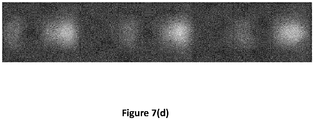
Figures 7(a) -(f) show the power density distribution in the xz- and xy-planes at wavelengths corresponding to the blue, green and red colors for a second periodic arrangement (figure 4(b) ) of double-material dielectric structure with
-
Figures 8(a) -(f) show the power density distribution in the xz- and xy-planes at wavelengths corresponding to the blue, green and red colors for a periodic arrangement (figure 4(a) ) of double-material dielectric structure with n 3 <
-
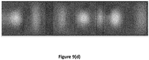
Figures 9(a) -(f) show the power density distribution in the xz- and xy-planes at wavelengths corresponding to the blue, green and red colors for a periodic arrangement (figure 4(b) ) of double-material dielectric structure with n 3 <
-
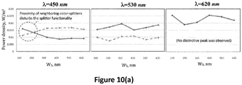
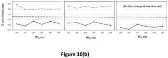
Figures 10 present a peak power density (a) and X-coordinate of NJ hot spot (b) versus W3 for the single (central) element of the array presented infigure 4(a) with such parameters n1=1, n2= 1.8, n3= 1.6, W1= W2= 600nm, H=1200nm, Z=1700nm; -
Figures 11 present a peak power density (a) and X-coordinate of NJ hot spot (b) versus W3 for the single (central) element of the array presented infigure 4(b) with such parameters n1=1, n2= 1.8, n3= 1.6, W1= W2=600nm, H=1200nm, Z=1700nm; -
Figures 12 present a peak power density (a) and X-coordinate of NJ hot spot (b) versus W3 for the single (central) element of the array presented infigure 4(a) with such parameters n1=1, n2= 2, n3= 1.2, W1= W2=600nm, H=1300nm, Z=1500nm; -
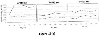
Figures 13 present a peak power density (a) and X-coordinate of NJ hot spot (b) versus W3 for the single (central) element of the array presented infigure 4(b) with such parameters n1=1, n2= 2, n3= 1.2, W1= W2=600nm, H=1300nm, Z=1500nm; -
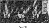
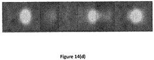
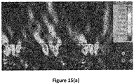
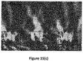
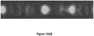
Figures 14(a) -(f) and 15(a)-(f) show the power density distribution in xz- and xy- for 1D arrays of NJ-based dielectric color splitters presented infigure 4(b) and Θ i = ±15° (i.e. for non-normal incident electromagnetic waves); -
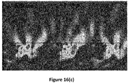
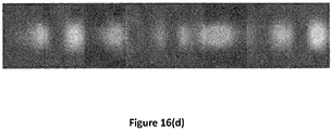
Figure 16(a) -(f) show the power density distribution in xz- and xy- for 1D arrays of NJ-based dielectric color splitters presented infigure 4(b) and Θ i = ±30° (i.e. for non-normal incident electromagnetic waves); -
Figures 17(a) and17(b) illustrate the splitting effect of the color splitter microstructures fromfigures 5(a) -(f) andfigures 6(a) -(f); -
Figure 18 presents an embodiment showing the 2D arrangement of the splitter elements on top of the regular 2D grid of the image sensor pixels, together with a suggested demosaicing function; -
Figure 19 presents an embodiment where a color splitter structure as previously presented partially covers at least two pixels; -
Figure 20 provides a cross-section view of a double-material structure with nonvertical edges. - The components in the figures are not necessarily to scale, emphasis instead being placed upon illustrating the principles of the invention.
- The present disclosure relates to a technique for splitting color-bands of an incident visible light by combining two or more dielectric materials with different refractive indexes (the refractive indexes of constitutive parts are higher than the surrounding material) in such a way that all the nanojets (NJ) beams, originating from different edges (associated with different blocks/layers) of the microstructure, recombine and contribute to the formation of a spectral-dependent NJ beam deflection.
- For reminders, the generation of NJ beams is described in document
EP3223 063 . Numerical simulations demonstrate that proposed principle of color splitting based on the NJ beam deflection can generate focused color images. The characteristics of the generated NJ beams are controlled by the parameters of the corresponding blocks, i.e. refractive index ratios between the blocks, dimensions of the blocks and angle of wave incidence. - In the following an element or structure that can perform such color splitting or deviating structure is a specific configuration of a more general design of a NJ beam forming element (also called hereafter a double-material structure) which is a combination of at least two dielectric materials with different refractive indexes having a nonsymmetrical or a symmetrical system in a vertical cross-section. Hereafter, structures having such a topology are referred to as structures based on a combination of different materials.
-
Figure 1 illustrates the cross-section view, in a XZ plane of a double-material structure 10 according to an embodiment of the present disclosure. - Such a double-material structure 10, in cross-section view, corresponds to a combination of two different blocks of materials, referenced 12 and 13.
Such blocks figure 1 ), but could also be trapezoidal or cuboid-shaped. - Blocks referenced 12 and 13 respectively have refractive indexes n 2 and n 3 (n 2 > n 3) embedded in a homogeneous
dielectric host medium 11 with a refractive index n 1 < n3. For simplicity, we assume that all the materials are lossless and non-dispersive. -
Blocks -
Block 12 has a width W1 and a height H, whileblock 13 has a width W2 and the same height H. - Hereafter, we consider that
blocks - The double-material structure 10, once it receives an incident light or
electromagnetic wave 14, generates several nanojets beams (the three nanojets beams NJ1, NJ2 and NJ3 generated respectively by edges of the double-material structure 10) that can intersect in different hot spots or focused points or locations referenced as points A, B and C. - According to the present disclosure, the materials and size of the
constitutive parts - In this Section, we present a set of equations to estimate the optimal combinations of materials and dimensions of the
blocks - As demonstrated in patent document
EP 3 223 063 in the name of the same Applicant, the beam-forming phenomenon appears on an edge between two materials of different refractive indexes, and is associated solely with this edge. The ratio of refractive indexes between both materials contributes to controlling an elevation angle of the generated nanojet beam, which is an angular position of a projection of the NJ beam in the vertical xz plane. Actually, the NJ beam radiation angle is defined by the Snell's law and can be determined using the approximate formula:

host medium 11, and n 2 is the refractive index of a part of the double-material structure. The point of intersection of two equal NJ beams radiated from the opposite sides of the element determines the focal length of the NJ structure. In a first approximation, in the case of a single material element the focal length of the NJ structure can be characterized as the function of the size (width) and index ratio of the media inside and outside the structure. The total radiated NJ beam will be directed along the symmetry axis of the system. - As illustrated in
figure 1 , when asecond element 13 with refractive index n 3 and width W 2, is attached in direct contact with thefirst element 12 with refractive index n2, the angle of NJ beam radiation from the boundary between bothelements 

- The NJ beam radiation angle at the third edge, between
block 13 andhost medium 11, corresponds to:

- Let us note that the length and intensity of these three NJs, generated by the three edges between the
materials figure 1 , it will be the NJ refracted at the angle Θ B1 generated at the boundary betweenblock 12 andhost medium 11. - The three nanojet beams generated at the boundaries between the materials of different refractive indexes of optical device 10 may partially or totally combine, to produce a total focused beam, which corresponds to the interference pattern caused by the three primary nanojet beams associated with the three edges of device 10.
- To explain the behavior of total NJs radiated by the double-material structure 10, we should determine the points of intersection (denoted A, B and C on
figure 1 ) of these initial, or primary, NJs associated with the edges of the system 10 and radiated at the angles Θ B1, Θ B2 and Θ B3. - The point A of first (NJ1) and second (NJ2) NJs' intersection has the coordinates (W A,H A), where:

- First (NJ1) and third (NJ3) NJs will intersect at a point B with the coordinates (W B,H B), where:

- It is necessary to note, that second (NJ2) and third (NJ3) nanojets will intersect only if


- Our numerical simulations presented below have demonstrated that spectral-dependent NJ beam deflection for 3 different wavelengths (λ1 <λ2 <λ3) is observed for W≅λ2 and H≅HB. For such parameters of the system, the direction of NJ deviation depends on the wavelength of incident wave. Particularly, we have observed that for

Figure 2(b) ) at λ =λ1 we obtain long intensive NJ deviated towards the part with lower refractive index n3. In this case the main input will be from the short but most intensive NJ associated with the right edge of the system inFigure 2(b) - NJ1. For a case of longer wavelengths (λ =λ2,3) the maximal total response will be determined by the input of the NJ2 and NJ3 beams which are longer but less intensive. As the result, the long intensive NJs will be deviated towards the part with higher refractive index n2. Taking
Figure 2(c) ) we observe the opposite situation. It will be demonstrated that at λ =λ1 the main input is NJ3 (for the chosen parameters NJ3 is less intensive than NJ1 and NJ2) and resulting NJ is deviated towards the part with higher refractive index n2. The most intensive NJ1 determines the response of the system at λ =λ2. For both discussed cases response of the system at λ =λ3 is related to the input of the NJs of medium intensity. - Here, we discuss the influence of the angle of plane wave incidence (Θ i ,
Fig.2d ) on the characteristics of proposed double-material NJ microlens. It is necessary to take into account that for oblique incidence the approximate formula for NJ beam radiation angles should be modified and will be presented in the form:
- Based on the identified properties of the structure depicted in the
figure 1 , it is proposed in the following to determine how to adapt the parameters of such structure (i.e. the refractive index values, and/or the width and/or the height of such structure) in order to obtain a color splitter function. Such color splitter function is of interest especially in the field of the image sensors. - Indeed, in one embodiment of the disclosure, it is possible to deviate color components (such as the blue, green and red components) of the light in different directions that can be later recorded by photodiodes in an image sensor.
- The
figures 2(a) -(d) present roughly the same structure as infigure 1 but adapted to the context of the color splitting problem. -
Figure 3 presents the power density distribution, for three different incident electromagnetic waves, having for respective wavelength A = 620 nm (i.e. red light), A = 530 nm (i.e. green light), and A = 450 nm (i.e. blue light), in xz-plane for the structure defined with such parameters: n1=1, n2= 1.8, n3= 1.6, W1= W2= 600nm; and H=1200nm. - Hence,
figure 3 presents the power density distribution in xz-plane with n 3 >
figure 3 , the height H of the structure is chosen such as H ≅ HB i.e. the focus point B is close to the surface of the structure. - It is possible to see 2 NJs (one NJ is the combination of NJ1 and NJ2) of different length situated above the constitutive parts of the structure. The length of these NJs is different (longest NJ is situated above the part with higher refractive index n 2). By selecting the height of the structure up to or around H ≅ HB we can observe redistribution of the power density between two generated NJs situated above the constitutive parts of the structure. As the result, we obtain that for λ = 450 nm right NJ will be longer than left. So, at some distance from the top surface of the element, we will observe that the spot for a blue color will be situated above the part with lower refractive index and the spots for green and red colors will be above the part with higher refractive index. Hence, the spectral-dependent NJ beam deflection takes place if H ≅ HB and focal point B for the NJs related to the external boundaries of the structure (NJ1 and NJ3) is close to the surface of structure or within the structure. Playing with the materials of the layers, we can change power density distribution for different colors.
- To study the mutual influence of the neighbouring NJs on the power density redistribution, we consider two different arrays of double-material structures. The investigated topologies are presented in
figures 4(a) and(b). First array (figure 4(a) ) corresponds to the periodic alternation of the double-material structures separated by the blocks with refractive index n 1 (in our numerical simulations n 1 is the refractive index of the host medium). We assume that W 3 is the width of this block (i.e. the block having a material with a refractive index equal to n 1). For the second array (figure 4(b) ) medium with refractive index n 1 separate the blocks with the same refractive indexes. -
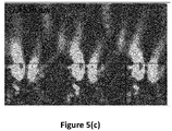
Figures 5(a) -(f) andfigures 6(a) -(f) illustrate power density distribution in the xz-and xy-planes at wavelengths corresponding to the blue, green and red colors for two arrays of double-material dielectric structures with
figure 4(b) ) the intensity of the NJ for blue color is higher and distance between the spots for green and red colors is bigger. So, second arrangement is preferable for color splitter application. - More precisely,
figures 5(a) , (c) and(e) present the power density distribution in a xz-plane (Y=0) for the array presented infigure 4(a) with such parameters: n1=1, n2= 1.8, n3= 1.6, W1= W2= W3= 600nm, H=1200nm. -
Figures 5(b) , (d) and(f) present the power density distribution xy-plane (Z=1700nm) for the array presented infigure 4(a) with such parameters: n1=1, n2= 1.8, n3= 1.6, W1= W2= W3= 600nm, H=1200nm. -
Figures 6(a) , (c) and(e) present the power density distribution in a xz-plane (Y=0) for the array presented infigure 4(b) with such parameters: n1=1, n2= 1.8, n3= 1.6, W1= W2= W3= 600nm, H=1200nm. -
Figures 6(b) , (d) and(f) present the power density distribution xy-plane (Z=1700nm) for the array presented infigure 4(b) with such parameters: n1=1, n2= 1.8, n3= 1.6, W1= W2= W3= 600nm, H=1200nm. - Hence, with the configuration described in
figures 6(a) -(f), we obtain a blue color splitting in the sense that the structure deviates the light associated with thewavelength 450 nm in one direction, and the other components in another direction. - Let us note that for double-material dielectric structure with

-
Figures 7(a) -(f) show the power density distribution in the xz- and xy-planes at wavelengths corresponding to the blue, green and red colors for a second periodic arrangement (figure 4(b) ) of double-material dielectric structure with
- Indeed,
figures 7(a) , (c) and(e) present the power density distribution in a xz-plane (Y=0) for the array presented infigure 4(a) with such parameters: n1=1, n2= 2, n3= 1.2, W1= W2= W3= 600nm, H=1300nm. -
Figures 7(b) , (d) and(f) present the power density distribution xy-plane (Z=1500nm) for the array presented infigure 4(a) with such parameters: n1=1, n2= 2, n3= 1.2, W1= W2= W3= 600nm, H=1300nm. - The neighbouring NJs more affect each other if we reduce the width W3 (
figures 8(a) -(f) andfigures 9(a) -(f); W3=200nm). We can see that for both arrays of structures the positions of the spots corresponding to the different colors will be changed. As the result, at the distance Z=1700nm we cannot easily distinguish the spots corresponding to the different colors. It is necessary to change the position of the detector. But for lower width W3, first arrangement is preferable. - Indeed,
figures 8(a) , (c) and(e) present the power density distribution in a xz-plane (Y=0) for the array presented infigure 4(a) with such parameters: n1=1, n2= 1.8, n3= 1.6, W1= W2= 600 nm and W3= 200nm, H=1200nm. -
Figures 8(b) , (d) and(f) present the power density distribution xy-plane (Z=1700nm) for the array presented infigure 4(a) with such parameters: n1=1, n2= 1.8, n3= 1.6, W1= W2= 600 nm and W3= 200nm, H=1200nm. -
Figures 9(a) , (c) and(e) present the power density distribution in a xz-plane (Y=0) for the array presented infigure 4(b) with such parameters: n1=1, n2= 1.8, n3= 1.6, W1= W2= 600 nm and W3= 200nm, H=1200nm. -
Figures 9(b) , (d) and(f) present the power density distribution xy-plane (Z=1700nm) for the array presented infigure 4(b) with such parameters: n1=1, n2= 1.8, n3= 1.6, W1= W2= 600 nm and W3= 200nm, H=1200nm. - To analyze the influence of the distance between the elements in the array on the color splitting phenomenon, we consider the dependence of peak power density and x-coordinate of the NJ hot spot on W3 (
figures 10(a) -(b) to 13(a)-(b)). The presented numerical data correspond to the single central element in two different arrays (seefigures 4(a) -(b)) of three double-material elements. It was assumed that boundary between the constitutive parts of the element corresponds to X=0. For the array presented infigure 4(a) (periodic array), left part (X<0) is the part with higher refractive index n2; for the array presented infigure 4(b) (medium with refractive index n1 separate the blocks with the same refractive indexes), left part is the part with lower refractive index n3. Almost in all considered cases we can observe 2 NJ hot spots of different power density above the constitutive parts of the elements. As the result of analysis of these Figures we can conclude that for the fixed wavelength the position of the hot spot is almost independent on the distance W3. At the same time, for a small distance W3 we can have power density redistribution affecting color separation. - Indeed,
figures 10 present a peak power density (a) and X-coordinate of NJ hot spot (b) versus W3 for the single (central) element of the array presented infigure 4(a) with such parameters n1=1, n2= 1.8, n3= 1.6, W1= W2= 600nm, H=1200nm, Z=1700nm. -
Figures 11 present a peak power density (a) and X-coordinate of NJ hot spot (b) versus W3 for the single (central) element of the array presented infigure 4(b) with such parameters n1=1, n2= 1.8, n3= 1.6, W1= W2=600nm, H=1200nm, Z=1700nm. -
Figures 12 present a peak power density (a) and X-coordinate of NJ hot spot (b) versus W3 for the single (central) element of the array presented infigure 4(a) with such parameters n1=1, n2= 2, n3= 1.2, W1= W2=600nm, H=1300nm, Z=1500nm. -
Figures 13 present a peak power density (a) and X-coordinate of NJ hot spot (b) versus W3 for the single (central) element of the array presented infigure 4(b) with such parameters n1=1, n2= 2, n3= 1.2, W1= W2=600nm, H=1300nm, Z=1500nm. - NJ field distribution dramatically changes with the angle of wave incidence. Let us consider the possibility to use double material dielectric structures for color splitting in the case of oblique incidence. It was observed that for oblique incidence, we have additional deviation of the NJs related to the edges of the system. So, the position of point B will be changed. The dispersion of NJ response and mutual influence of the neighbouring NJs will lead to the shift of the spots corresponding to the different colors and totally new redistribution of the power density.
Figures 14(a) -(f) and 15(a)-(f) show the power density distribution in xz- and xy- for 1D arrays of NJ-based dielectric color splitters presented infigure 4(b) and Θ i = ±15°. We can distinguish intensive spots corresponding to the blue and red colors above different structures for the detector at Z=1400nm. The periodic arrays (figure 4(a) ) does not provide color splitting function. -
Figures 14(a) , (c) and(e) present the power density distribution in a xz-plane (Y=0) for the array presented infigure 4(b) with such parameters: n1=1, n2= 1.8, n3= 1.6, W1= W2=W3= 600 nm, H=1180 nm and Θ i = 15°. -
Figures 14(b) , (d) and(f) present the power density distribution xy-plane (Z=1400nm) for the array presented infigure 4(b) with such parameters: n1=1, n2= 1.8, n3= 1.6, W1= W2=W3= 600 nm, H=1180 nm and Θ i = 15°. -
Figures 15(a) , (c) and(e) present the power density distribution in a xz-plane (Y=0) for the array presented infigure 4(b) with such parameters: n1=1, n2= 1.8, n3= 1.6, W1= W2=W3= 600 nm, H=1180 nm and Θ i = -15°. -
Figures 15(b) , (d) and(f) present the power density distribution xy-plane (Z=1700nm) for the array presented infigure 4(b) with such parameters: n1=1, n2= 1.8, n3= 1.6, W1= W2=W3= 600 nm, H=1180 nm and Θ i = -15°. - Increasing the angle of electromagnetic wave incidence (
figures 16(a) , (c) and(e), with Θ i = ±30°), we still can obtain desirable optical function. In this case the distance between the intensive spots corresponding to the blue and red colors will be small. -
Figures 16(a) , (c) and(e) present the power density distribution in a xz-plane (Y=0) for the array presented infigure 4(b) with such parameters: n1=1, n2= 1.8, n3= 1.6, W1= W2=W3= 600 nm, H=1100 nm and Θ i = 30°. -
Figures 16(b) , (d) and(f) present the power density distribution xy-plane (Z=1300nm) for the array presented infigure 4(b) with such parameters: n1=1, n2= 1.8, n3= 1.6, W1= W2=W3= 600 nm, H=1100 nm and Θ i = 30°. - In this section, we propose one embodiment that uses the designs in the previous section (5.2.4) to realize a full 2D arrangement of the color splitter elements on top of the image sensor pixels.
Figures 17(a) and17(b) illustrate the splitting effect of the color splitter microstructures fromfigures 5(a) -(f) andfigures 6(a) -(f).Figure 17(a) shows the case where the green (λ = 530 nm) and red (λ = 620 nm) wavelengths are deflected to one direction and the blue wavelength (λ = 450 nm) to the opposite direction. We name the color splitting result of this splitter structure as "blue separation".Figure 17(b) shows the case where the green (λ = 530 nm) and blue (λ = 450 nm) wavelengths are deflected to one direction and the red wavelength (λ = 620 nm) to the opposite direction. We name the color splitting result of this splitter structure as "red separation". -
Figures 17(a) presents a blue separation, as the result of a color splitter design demonstrated infigures 5(a) -(f). -
Figures 17(b) presents a red separation, as the result of a color splitter design demonstrated infigures 7(a) -(f). -
Figure 18 presents an embodiment showing the 2D arrangement of the splitter elements on top of the regular 2D grid of the image sensor pixels, together with a suggested demosaicing function. - This embodiment uses the two types of color splitter structures shown
figures 17(a) and17(b) , one tailored for the "blue separation" and the other one tailored for the "red separation" functionality.Figure 18 also illustrates the light components received by each pixel on the image sensor together with a suggested demosaicing function. -
Figure 19 presents an embodiment where a color splitter structure as previously presented partially covers at least two pixels. - It is possible to design a color splitter structure that can "deviate" electromagnetic waves with a specific wavelength λ1 and that can deviate in another direction light having a spectrum in which no or few electromagnetic waves having a wavelength equal to λ1 are present. Hence, each pixel (between
pixel 1 and pixel 2) record a different value, for different colors. In a variant, a conventional color filter is added at the top of the photosensitive material in order to filter residual electromagnetic waves. -
Figure 20 provides a cross-section view of a double-material structure with nonvertical edges. - In this subsection, we consider the structures with nonvertical edges and top/bottom surface parallel to xy-plane. Let us assume that αi (with i equals to 1, 2 or 3) are the base angles for a double-material system. The general topology of the double-material NJ structure is illustrated in
figure 20 . This cross-section view may correspond to the double-material prismatic system embedded in a homogeneous dielectric host media with a refractive index n 1 < n 2< n 3. - For the structure with the base angles αi (with i equals to 1, 2 or 3) the NJ beam radiation angle Θ Bj can be determined using the approximate formula (08):


- To explain the behavior of total NJs radiated by the double-material structure 10 we should substitute these expressions for NJ radiation angles into the formulas (04)-(07).
- In the case of the system with nonvertical edges the main performance characteristics of the double-material system discussed before are preserved.
- The change of the base angle will change the direction of the NJs and so it affects the crossing points of the nanojet and the color splitting effect. The design rule for a color splitter with non-vertical base angle is to calculate the new NJ deviation angles, and the calculate the height HB in which the crossing of the NJs happen and then choose H equal to HB to acheive the color splitting effect.
- More precisely, to explain the behavior of total NJs radiated by the double-material structure we should substitute new expressions for NJ radiation angles into the formulas (4)-(7). This will give us the coordinates of the cross sections of the NJ beams (points A, B and C in
Fig. 1 ). We use the same design rule to get color separation property for the case of the double material element with non-vertical base angles: the spectral-dependent NJ beam deflection (the color splitting functionality) takes place if H ≈ HB and focal point B for the NJs related to the external boundaries of the system (NJ1 and NJ3) is close to the surface of microlens or within the system. The only difference will be that the value for HB is calculated using the modified formula (Eq. 09) for the NJ beam angles.
Claims (16)
- An image sensor comprising pixels for acquiring color information from incoming visible light, wherein said image sensor being associated with a three-dimensional cartesian coordinate system defined by axis x, y and z, wherein the z-axis being normal to said image sensor, said image sensor comprising at least two pixels being partially covered by a color splitter structure comprising a first part and a second part, that are positioned side by side along said x-axis, and each of said first and second parts being adjacent to a dielectric part along said x-axis, each of said dielectric part having a first refractive index n 1, said first part having a second refractive index n 2, and said second part having a third refractive index n 3, wherein n 1 < n 3 < n 2, and wherein according to a cross section with a plane xz, the first part of said color splitter structure has a first width W 1 along the x-axis, a height H along the z-axis and the second part of said color splitter structure has a second width W 2 along the x-axis, and the same height H along the z-axis , and wherein said color splitter structure further comprises, according to said cross-section:- a first edge between one of said dielectric parts and said first part of said color splitter structure along said z-axis that can generate a first beam (NJ1) in a near field zone;- a second edge between said first part of said color splitter structure and said second part of said color splitter structure along said z-axis that can generate a second beam (NJ2) in a near field zone;- a third edge between said second part of said color splitter structure and one of said dielectric parts along said z-axis that can generate a third beam (NJ3) in a near field zone,wherein said height H is close to a value

- The image sensor according to claim 1, wherein

- The image sensor according to claim 1, wherein n 3 >

- The image sensor according to claim 1, wherein

- The image sensor according to claim 1, wherein

- The image sensor according to any claims 1 to 5, wherein said visible light comprises electromagnetic waves having wavelengths that go from 390 nm to 700 nm.
- The image sensor according to any claims 1,3 or 5, wherein said wavelength λ1 belongs to range [390 nm, 450 nm].
- The image sensor according to any claims 1, 2 or 4, wherein said wavelength λ1 belongs to range [620 nm, 700 nm].
- The image sensor according to any claims 1 to 8, wherein said first width W 1 and said second width W 2 are equal to each other.
- The image sensor according to any claims 1 to 9, wherein each pair of pixels is partially covered by a structure identical to said color splitter structure.
- The image sensor according to any claims 1 to 9, wherein each pair of pixels is partially covered by a structure that is alternatively either a structure identical to said color splitter structure, or a structure comprising first and second parts which are inverted compared to said color splitter structure.
- The image sensor according to any claims 10 to 11, wherein each successive structure is separated by an identical dielectric part having a width, along the x-axis, equal to W 3, and wherein the value of W 3 is comprised between 250 nm and 600 nm.
- The image sensor according to any claims 1 to 12, wherein each first and second part, and said dielectric part are made of a material that belongs to the group comprising:- glass;- plastic;- a polymer material;- oxides;- nitrides.
- The image sensor according to any claims 1 to 13, wherein at least one pixel of said at least two pixels further comprises conventional color filter positioned between said color splitter structure and photosensitive materials associated with each of said at least two pixels.
- The image sensor according to any claims 1 to 14, wherein said height H is around ±5% of the value HB.
- The image sensor according to any claims 1 to 15, wherein said radiation angles of said first and said third beams Θ B1 and Θ B3 are equal to

Priority Applications (7)
| Application Number | Priority Date | Filing Date | Title |
|---|---|---|---|
| EP18305265.3A EP3540499A1 (en) | 2018-03-13 | 2018-03-13 | Image sensor comprising a color splitter with two different refractive indexes |
| JP2020548739A JP7339271B2 (en) | 2018-03-13 | 2019-03-08 | Image sensor containing a color splitter with two different refractive indices |
| CN201980029966.9A CN112219153B (en) | 2018-03-13 | 2019-03-08 | Image sensor comprising a color separator having two different refractive indices |
| EP19708560.8A EP3765893A1 (en) | 2018-03-13 | 2019-03-08 | Image sensor comprising a color splitter with two different refractive indexes |
| PCT/EP2019/055905 WO2019175062A1 (en) | 2018-03-13 | 2019-03-08 | Image sensor comprising a color splitter with two different refractive indexes |
| RU2020132589A RU2020132589A (en) | 2018-03-13 | 2019-03-08 | IMAGE SENSOR CONTAINING A COLOR SEPARATOR WITH TWO DIFFERENT REFRACTIVE INDICES |
| US16/980,326 US11604363B2 (en) | 2018-03-13 | 2019-03-08 | Image sensor comprising a color splitter with two different refractive indexes |
Applications Claiming Priority (1)
| Application Number | Priority Date | Filing Date | Title |
|---|---|---|---|
| EP18305265.3A EP3540499A1 (en) | 2018-03-13 | 2018-03-13 | Image sensor comprising a color splitter with two different refractive indexes |
Publications (1)
| Publication Number | Publication Date |
|---|---|
| EP3540499A1 true EP3540499A1 (en) | 2019-09-18 |
Family
ID=62631034
Family Applications (2)
| Application Number | Title | Priority Date | Filing Date |
|---|---|---|---|
| EP18305265.3A Withdrawn EP3540499A1 (en) | 2018-03-13 | 2018-03-13 | Image sensor comprising a color splitter with two different refractive indexes |
| EP19708560.8A Pending EP3765893A1 (en) | 2018-03-13 | 2019-03-08 | Image sensor comprising a color splitter with two different refractive indexes |
Family Applications After (1)
| Application Number | Title | Priority Date | Filing Date |
|---|---|---|---|
| EP19708560.8A Pending EP3765893A1 (en) | 2018-03-13 | 2019-03-08 | Image sensor comprising a color splitter with two different refractive indexes |
Country Status (6)
| Country | Link |
|---|---|
| US (1) | US11604363B2 (en) |
| EP (2) | EP3540499A1 (en) |
| JP (1) | JP7339271B2 (en) |
| CN (1) | CN112219153B (en) |
| RU (1) | RU2020132589A (en) |
| WO (1) | WO2019175062A1 (en) |
Cited By (2)
| Publication number | Priority date | Publication date | Assignee | Title |
|---|---|---|---|---|
| US11573356B2 (en) | 2018-03-13 | 2023-02-07 | Interdigital Ce Patent Holdings | Diffraction grating comprising double-materials structures |
| US11604363B2 (en) | 2018-03-13 | 2023-03-14 | Interdigital Ce Patent Holdings | Image sensor comprising a color splitter with two different refractive indexes |
Families Citing this family (3)
| Publication number | Priority date | Publication date | Assignee | Title |
|---|---|---|---|---|
| EP3591700A1 (en) * | 2018-07-02 | 2020-01-08 | Thomson Licensing | Image sensor comprising a color splitter with two different refractive indexes, and different height |
| EP3671310A1 (en) * | 2018-12-18 | 2020-06-24 | Thomson Licensing | Optical manipulation apparatus for trapping or moving micro or nanoparticles |
| WO2022023170A1 (en) | 2020-07-30 | 2022-02-03 | Interdigital Ce Patent Holdings, Sas | Color splitter system |
Citations (3)
| Publication number | Priority date | Publication date | Assignee | Title |
|---|---|---|---|---|
| US20130099343A1 (en) * | 2010-07-02 | 2013-04-25 | Panasonic Corporation | Solid-state imaging device |
| EP3223063A1 (en) | 2016-03-24 | 2017-09-27 | Thomson Licensing | Device for forming a field intensity pattern in the near zone, from incident electromagnetic waves |
| EP3223062A1 (en) * | 2016-03-24 | 2017-09-27 | Thomson Licensing | Device for forming at least one focused beam in the near zone, from incident electromagnetic waves |
Family Cites Families (71)
| Publication number | Priority date | Publication date | Assignee | Title |
|---|---|---|---|---|
| US3718383A (en) | 1971-04-19 | 1973-02-27 | Eastman Kodak Co | Plastic optical element having refractive index gradient |
| JP3891628B2 (en) | 1997-02-04 | 2007-03-14 | オリンパス株式会社 | Illumination optical system and endoscope system including the same |
| CN1526079A (en) | 2001-07-10 | 2004-09-01 | 住友电气工业株式会社 | Optical waveguide type defraction grating device and a method of manufacturing thereof |
| WO2003025635A1 (en) | 2001-09-19 | 2003-03-27 | Technion Research & Development Foundation Ltd. | Space-variant subwavelength dielectric grating and applications thereof |
| WO2004027464A1 (en) | 2002-09-19 | 2004-04-01 | Sumitomo Electric Industries, Ltd. | Diffractive optical device and method for producing same |
| FI115169B (en) | 2003-05-13 | 2005-03-15 | Nokia Corp | Method and optical system for coupling light to a waveguide |
| KR100597039B1 (en) | 2004-02-26 | 2006-07-04 | 에이에스엠엘 네델란즈 비.브이. | Stationary and dynamic radial transverse electric polarizer device for high numerical aperture systems, lithographic projection apparatus and manufacturing method of the same |
| US7456384B2 (en) * | 2004-12-10 | 2008-11-25 | Sony Corporation | Method and apparatus for acquiring physical information, method for manufacturing semiconductor device including array of plurality of unit components for detecting physical quantity distribution, light-receiving device and manufacturing method therefor, and solid-state imaging device and manufacturing method therefor |
| EP1932050A2 (en) | 2005-09-14 | 2008-06-18 | Mirage Innovations Ltd. | Diffractive optical device and system |
| JP4893200B2 (en) | 2006-09-28 | 2012-03-07 | ブラザー工業株式会社 | Optical system for light beam transfer, and retinal scanning display using the same |
| US8212859B2 (en) | 2006-10-13 | 2012-07-03 | Apple Inc. | Peripheral treatment for head-mounted displays |
| US7394535B1 (en) | 2007-03-20 | 2008-07-01 | Tokyo Electron Limited | Optical metrology using a photonic nanojet |
| WO2009083977A2 (en) | 2008-01-02 | 2009-07-09 | Mirage Innovations Ltd. | Optical device for relaying polychromatic light |
| US8717669B2 (en) | 2008-10-17 | 2014-05-06 | The Arizona Board Of Regents | Apparatus and method of generating nearly non-diffracting beams from multimode optical fibers |
| EP2196729A1 (en) | 2008-12-12 | 2010-06-16 | BAE Systems PLC | Improvements in or relating to waveguides |
| JP6007830B2 (en) | 2012-03-26 | 2016-10-12 | 旭硝子株式会社 | Transmission diffraction element |
| US8989535B2 (en) | 2012-06-04 | 2015-03-24 | Microsoft Technology Licensing, Llc | Multiple waveguide imaging structure |
| US9140602B2 (en) | 2012-08-11 | 2015-09-22 | The Board Of Trustees Of The Leland Stanford Junior University | Nanophotonic light-field sensor |
| US8885997B2 (en) | 2012-08-31 | 2014-11-11 | Microsoft Corporation | NED polarization system for wavelength pass-through |
| JP6094832B2 (en) | 2012-09-03 | 2017-03-15 | パナソニックIpマネジメント株式会社 | Solid-state imaging device and imaging apparatus |
| FI125270B (en) | 2012-09-20 | 2015-08-14 | Teknologian Tutkimuskeskus Vtt Oy | Optical device with diffractive grating |
| WO2014061173A1 (en) | 2012-10-18 | 2014-04-24 | パナソニック株式会社 | Solid-state imaging element |
| WO2014176277A1 (en) | 2013-04-22 | 2014-10-30 | Cornell University | Athermal optical devices based on composite structures |
| US10371898B2 (en) | 2013-09-05 | 2019-08-06 | Southern Methodist University | Enhanced coupling strength grating having a cover layer |
| KR102276432B1 (en) * | 2014-04-07 | 2021-07-09 | 삼성전자주식회사 | Color separation device and image sensor including the color separation device |
| KR102159166B1 (en) * | 2014-05-09 | 2020-09-23 | 삼성전자주식회사 | Color separation device and image sensor including the color separation device |
| US9726794B2 (en) | 2014-06-13 | 2017-08-08 | The Regents Of The University Of California | High index contrast grating structure for light manipulation and related method |
| KR102261855B1 (en) | 2014-06-13 | 2021-06-07 | 삼성전자주식회사 | Stacked image sensor including color separation element and image pickup apparatus including the stacked image sensor |
| GB2529003B (en) | 2014-08-03 | 2020-08-26 | Wave Optics Ltd | Optical device |
| KR20160023158A (en) | 2014-08-21 | 2016-03-03 | 삼성전자주식회사 | Image sensor having improved light utilization efficiency and method of manufacturing the same |
| KR102323204B1 (en) | 2014-08-22 | 2021-11-08 | 삼성전자주식회사 | Image sensor vividly embodying color and method of manufacturing the same |
| US20160064172A1 (en) | 2014-09-02 | 2016-03-03 | Delta Systems, Inc. | Plunger switch assembly and method of operation |
| KR102307458B1 (en) | 2014-10-20 | 2021-09-30 | 삼성전자주식회사 | Color splitter and method for manufacturing the same and image sensor including the same |
| US9513480B2 (en) | 2015-02-09 | 2016-12-06 | Microsoft Technology Licensing, Llc | Waveguide |
| EP3113478A1 (en) | 2015-06-30 | 2017-01-04 | Thomson Licensing | Plenoptic foveated camera |
| US10431624B2 (en) | 2015-07-08 | 2019-10-01 | Samsung Electronics Co., Ltd. | Method of manufacturing image sensor including nanostructure color filter |
| US10866360B2 (en) | 2015-08-19 | 2020-12-15 | President And Fellows Of Harvard College | Broadband multifunctional efficient meta-gratings based on dielectric waveguide phase shifters |
| EP3339938A4 (en) | 2015-08-20 | 2019-05-01 | Hoya Lens Thailand Ltd. | Optical device |
| KR102501643B1 (en) | 2015-09-24 | 2023-02-20 | 삼성전자주식회사 | Optical device having high refractive index optical functional layer and method of fabricating the same |
| KR102519178B1 (en) | 2015-09-25 | 2023-04-06 | 삼성전자주식회사 | Image sensor including color separation element and image pickup apparatus including the image sensor |
| KR102465995B1 (en) | 2015-09-30 | 2022-11-25 | 삼성전자주식회사 | Color splitter structure, method of manufacturing the same, image sensor including color splitter structure and optical apparatus including image sensor |
| KR102556008B1 (en) * | 2015-10-06 | 2023-07-17 | 삼성전자주식회사 | Color splitter of image sensor |
| KR102409389B1 (en) | 2015-10-06 | 2022-06-15 | 삼성전자주식회사 | Image sensor including color separation element |
| KR102561097B1 (en) | 2015-12-22 | 2023-07-28 | 삼성전자주식회사 | Color separation element array, image sensor having the same, and electronic apparatus |
| US9927614B2 (en) | 2015-12-29 | 2018-03-27 | Microsoft Technology Licensing, Llc | Augmented reality display system with variable focus |
| US9720237B1 (en) | 2016-01-27 | 2017-08-01 | Microsoft Technology Licensing, Llc. | Mixed environment display device and waveguide cross-coupling suppressors |
| US9891436B2 (en) | 2016-02-11 | 2018-02-13 | Microsoft Technology Licensing, Llc | Waveguide-based displays with anti-reflective and highly-reflective coating |
| US9791703B1 (en) | 2016-04-13 | 2017-10-17 | Microsoft Technology Licensing, Llc | Waveguides with extended field of view |
| US10197804B2 (en) | 2016-04-25 | 2019-02-05 | Microsoft Technology Licensing, Llc | Refractive coating for diffractive optical elements |
| US10061124B2 (en) | 2016-04-29 | 2018-08-28 | Microsoft Technology Licensing, Llc | Robust architecture for large field of view components |
| EP3240046A1 (en) | 2016-04-29 | 2017-11-01 | BASF Coatings GmbH | Solar light collector |
| US11204452B2 (en) | 2016-10-05 | 2021-12-21 | Agency For Science, Technology And Research | Diffractive optical element and method of forming thereof |
| EP3312674A1 (en) | 2016-10-21 | 2018-04-25 | Thomson Licensing | A photolithography device for generating pattern on a photoresist substrate |
| EP3312646A1 (en) | 2016-10-21 | 2018-04-25 | Thomson Licensing | Device and method for shielding at least one sub-wavelength-scale object from an incident electromagnetic wave |
| EP3312660A1 (en) | 2016-10-21 | 2018-04-25 | Thomson Licensing | Device for forming at least one tilted focused beam in the near zone, from incident electromagnetic waves |
| NZ752202A (en) | 2016-10-26 | 2023-11-24 | Magic Leap Inc | Outcoupling grating for augmented reality system |
| CN113703270B (en) | 2016-12-01 | 2023-02-17 | 奇跃公司 | Projector with scanning array light engine |
| WO2018102834A2 (en) | 2016-12-02 | 2018-06-07 | Digilens, Inc. | Waveguide device with uniform output illumination |
| CN106772734A (en) | 2017-01-03 | 2017-05-31 | 中国科学院上海光学精密机械研究所 | The asymmetric pattern reflection type optical grid of broadband high-diffraction efficiency |
| CN110300912B (en) | 2017-02-15 | 2022-09-02 | 奇跃公司 | Projector architecture including artifact mitigation |
| EP3385219B1 (en) | 2017-04-07 | 2021-07-14 | InterDigital CE Patent Holdings | Method for manufacturing a device for forming at least one focused beam in a near zone |
| US10534115B1 (en) | 2017-09-22 | 2020-01-14 | Facebook Technologies, Llc | Gray-tone electron-beam lithography |
| CA3078522A1 (en) | 2017-10-20 | 2019-04-25 | Magic Leap, Inc. | Configuring optical layers in imprint lithography processes |
| EP3499278A1 (en) | 2017-12-13 | 2019-06-19 | Thomson Licensing | A diffraction grating structure comprising several grating lines |
| EP3540479A1 (en) | 2018-03-13 | 2019-09-18 | Thomson Licensing | Diffraction grating comprising double-materials structures |
| EP3540499A1 (en) | 2018-03-13 | 2019-09-18 | Thomson Licensing | Image sensor comprising a color splitter with two different refractive indexes |
| EP3588150A1 (en) | 2018-06-29 | 2020-01-01 | Thomson Licensing | An optical device comprising multi-layer waveguides |
| EP3591700A1 (en) | 2018-07-02 | 2020-01-08 | Thomson Licensing | Image sensor comprising a color splitter with two different refractive indexes, and different height |
| EP3671322A1 (en) | 2018-12-18 | 2020-06-24 | Thomson Licensing | Device for forming an outgoing electromagnetic wave from an incident electromagnetic wave |
| EP3671293A1 (en) | 2018-12-21 | 2020-06-24 | Thomson Licensing | An optical device comprising at least one diffraction grating having a grating pitch above the wavelength |
| EP4031927A1 (en) | 2019-09-19 | 2022-07-27 | InterDigital CE Patent Holdings | Optical device for coupling a high field of view of incident light |
-
2018
- 2018-03-13 EP EP18305265.3A patent/EP3540499A1/en not_active Withdrawn
-
2019
- 2019-03-08 JP JP2020548739A patent/JP7339271B2/en active Active
- 2019-03-08 EP EP19708560.8A patent/EP3765893A1/en active Pending
- 2019-03-08 CN CN201980029966.9A patent/CN112219153B/en active Active
- 2019-03-08 RU RU2020132589A patent/RU2020132589A/en unknown
- 2019-03-08 WO PCT/EP2019/055905 patent/WO2019175062A1/en unknown
- 2019-03-08 US US16/980,326 patent/US11604363B2/en active Active
Patent Citations (3)
| Publication number | Priority date | Publication date | Assignee | Title |
|---|---|---|---|---|
| US20130099343A1 (en) * | 2010-07-02 | 2013-04-25 | Panasonic Corporation | Solid-state imaging device |
| EP3223063A1 (en) | 2016-03-24 | 2017-09-27 | Thomson Licensing | Device for forming a field intensity pattern in the near zone, from incident electromagnetic waves |
| EP3223062A1 (en) * | 2016-03-24 | 2017-09-27 | Thomson Licensing | Device for forming at least one focused beam in the near zone, from incident electromagnetic waves |
Non-Patent Citations (1)
| Title |
|---|
| VICTOR V. KOTLYAR ET AL: "Photonic nanojets generated using square-profile microsteps", APPLIED OPTICS, vol. 53, no. 24, 20 August 2014 (2014-08-20), WASHINGTON, DC; US, pages 5322, XP055357764, ISSN: 0003-6935, DOI: 10.1364/AO.53.005322 * |
Cited By (2)
| Publication number | Priority date | Publication date | Assignee | Title |
|---|---|---|---|---|
| US11573356B2 (en) | 2018-03-13 | 2023-02-07 | Interdigital Ce Patent Holdings | Diffraction grating comprising double-materials structures |
| US11604363B2 (en) | 2018-03-13 | 2023-03-14 | Interdigital Ce Patent Holdings | Image sensor comprising a color splitter with two different refractive indexes |
Also Published As
| Publication number | Publication date |
|---|---|
| RU2020132589A (en) | 2022-04-04 |
| CN112219153B (en) | 2023-07-18 |
| US20210041709A1 (en) | 2021-02-11 |
| JP7339271B2 (en) | 2023-09-05 |
| EP3765893A1 (en) | 2021-01-20 |
| US11604363B2 (en) | 2023-03-14 |
| CN112219153A (en) | 2021-01-12 |
| JP2021517765A (en) | 2021-07-26 |
| WO2019175062A1 (en) | 2019-09-19 |
Similar Documents
| Publication | Publication Date | Title |
|---|---|---|
| US11604363B2 (en) | Image sensor comprising a color splitter with two different refractive indexes | |
| JP4455677B2 (en) | Photodetection device for imaging | |
| JP4264465B2 (en) | Photodetection device for imaging | |
| JP7396898B2 (en) | Apparatus and method for infrared multispectral imaging | |
| RU2607727C2 (en) | Photoelectric conversion device and imaging system | |
| US10393576B2 (en) | Image sensor including color filter isolation layer and method of manufacturing the same | |
| US9853073B2 (en) | Image sensor for producing vivid colors and method of manufacturing the same | |
| US9099370B2 (en) | Solid-state imaging element and imaging device | |
| EP2037298A1 (en) | Optical member and optical device comprising the same | |
| JP5188107B2 (en) | Array type photo detector | |
| KR102395775B1 (en) | Image sensor including color filter and method of fabricating the same | |
| EP3513229A1 (en) | Metasurface lens assembly for chromatic separation | |
| US20210233291A1 (en) | Image sensor comprising a color splitter with two different refractive indexes, and different height | |
| JP2015215616A (en) | Color separation element and image sensor including color separation element | |
| US10276612B2 (en) | Photoelectric conversion apparatus and image pickup system | |
| US11158661B2 (en) | Image sensor with micro-structured color filter | |
| WO2022023170A1 (en) | Color splitter system | |
| CN104166228B (en) | Digital holography microscope | |
| JP2017167115A (en) | Optical detection device | |
| CN105575985A (en) | Semiconductor optical sensor | |
| KR20110065178A (en) | Microlens of image sensor and manufacturing method of microlens of image sensor |
Legal Events
| Date | Code | Title | Description |
|---|---|---|---|
| PUAI | Public reference made under article 153(3) epc to a published international application that has entered the european phase |
Free format text: ORIGINAL CODE: 0009012 |
|
| AK | Designated contracting states |
Kind code of ref document: A1 Designated state(s): AL AT BE BG CH CY CZ DE DK EE ES FI FR GB GR HR HU IE IS IT LI LT LU LV MC MK MT NL NO PL PT RO RS SE SI SK SM TR |
|
| AX | Request for extension of the european patent |
Extension state: BA ME |
|
| RAP1 | Party data changed (applicant data changed or rights of an application transferred) |
Owner name: INTERDIGITAL CE PATENT HOLDINGS |
|
| STAA | Information on the status of an ep patent application or granted ep patent |
Free format text: STATUS: THE APPLICATION IS DEEMED TO BE WITHDRAWN |
|
| 18D | Application deemed to be withdrawn |
Effective date: 20200603 |