EP3540335A1 - Heat dissipation apparatus, terminal, and control method for heat dissipation apparatus - Google Patents
Heat dissipation apparatus, terminal, and control method for heat dissipation apparatus Download PDFInfo
- Publication number
- EP3540335A1 EP3540335A1 EP17929627.2A EP17929627A EP3540335A1 EP 3540335 A1 EP3540335 A1 EP 3540335A1 EP 17929627 A EP17929627 A EP 17929627A EP 3540335 A1 EP3540335 A1 EP 3540335A1
- Authority
- EP
- European Patent Office
- Prior art keywords
- conductive layer
- electric field
- heat dissipation
- dissipation device
- power supply
- Prior art date
- Legal status (The legal status is an assumption and is not a legal conclusion. Google has not performed a legal analysis and makes no representation as to the accuracy of the status listed.)
- Ceased
Links
Images



Classifications
-
- H—ELECTRICITY
- H05—ELECTRIC TECHNIQUES NOT OTHERWISE PROVIDED FOR
- H05K—PRINTED CIRCUITS; CASINGS OR CONSTRUCTIONAL DETAILS OF ELECTRIC APPARATUS; MANUFACTURE OF ASSEMBLAGES OF ELECTRICAL COMPONENTS
- H05K7/00—Constructional details common to different types of electric apparatus
- H05K7/20—Modifications to facilitate cooling, ventilating, or heating
-
- F—MECHANICAL ENGINEERING; LIGHTING; HEATING; WEAPONS; BLASTING
- F25—REFRIGERATION OR COOLING; COMBINED HEATING AND REFRIGERATION SYSTEMS; HEAT PUMP SYSTEMS; MANUFACTURE OR STORAGE OF ICE; LIQUEFACTION SOLIDIFICATION OF GASES
- F25B—REFRIGERATION MACHINES, PLANTS OR SYSTEMS; COMBINED HEATING AND REFRIGERATION SYSTEMS; HEAT PUMP SYSTEMS
- F25B21/00—Machines, plants or systems, using electric or magnetic effects
-
- F—MECHANICAL ENGINEERING; LIGHTING; HEATING; WEAPONS; BLASTING
- F25—REFRIGERATION OR COOLING; COMBINED HEATING AND REFRIGERATION SYSTEMS; HEAT PUMP SYSTEMS; MANUFACTURE OR STORAGE OF ICE; LIQUEFACTION SOLIDIFICATION OF GASES
- F25B—REFRIGERATION MACHINES, PLANTS OR SYSTEMS; COMBINED HEATING AND REFRIGERATION SYSTEMS; HEAT PUMP SYSTEMS
- F25B49/00—Arrangement or mounting of control or safety devices
-
- F—MECHANICAL ENGINEERING; LIGHTING; HEATING; WEAPONS; BLASTING
- F28—HEAT EXCHANGE IN GENERAL
- F28F—DETAILS OF HEAT-EXCHANGE AND HEAT-TRANSFER APPARATUS, OF GENERAL APPLICATION
- F28F13/00—Arrangements for modifying heat-transfer, e.g. increasing, decreasing
-
- H—ELECTRICITY
- H04—ELECTRIC COMMUNICATION TECHNIQUE
- H04M—TELEPHONIC COMMUNICATION
- H04M1/00—Substation equipment, e.g. for use by subscribers
- H04M1/72—Mobile telephones; Cordless telephones, i.e. devices for establishing wireless links to base stations without route selection
- H04M1/725—Cordless telephones
-
- H—ELECTRICITY
- H05—ELECTRIC TECHNIQUES NOT OTHERWISE PROVIDED FOR
- H05K—PRINTED CIRCUITS; CASINGS OR CONSTRUCTIONAL DETAILS OF ELECTRIC APPARATUS; MANUFACTURE OF ASSEMBLAGES OF ELECTRICAL COMPONENTS
- H05K1/00—Printed circuits
- H05K1/02—Details
- H05K1/0201—Thermal arrangements, e.g. for cooling, heating or preventing overheating
- H05K1/0203—Cooling of mounted components
- H05K1/0209—External configuration of printed circuit board adapted for heat dissipation, e.g. lay-out of conductors, coatings
-
- H—ELECTRICITY
- H10—SEMICONDUCTOR DEVICES; ELECTRIC SOLID-STATE DEVICES NOT OTHERWISE PROVIDED FOR
- H10W—GENERIC PACKAGES, INTERCONNECTIONS, CONNECTORS OR OTHER CONSTRUCTIONAL DETAILS OF DEVICES COVERED BY CLASS H10
- H10W40/00—Arrangements for thermal protection or thermal control
- H10W40/10—Arrangements for heating
-
- F—MECHANICAL ENGINEERING; LIGHTING; HEATING; WEAPONS; BLASTING
- F25—REFRIGERATION OR COOLING; COMBINED HEATING AND REFRIGERATION SYSTEMS; HEAT PUMP SYSTEMS; MANUFACTURE OR STORAGE OF ICE; LIQUEFACTION SOLIDIFICATION OF GASES
- F25B—REFRIGERATION MACHINES, PLANTS OR SYSTEMS; COMBINED HEATING AND REFRIGERATION SYSTEMS; HEAT PUMP SYSTEMS
- F25B2321/00—Details of machines, plants or systems, using electric or magnetic effects
- F25B2321/001—Details of machines, plants or systems, using electric or magnetic effects by using electro-caloric effects
-
- F—MECHANICAL ENGINEERING; LIGHTING; HEATING; WEAPONS; BLASTING
- F25—REFRIGERATION OR COOLING; COMBINED HEATING AND REFRIGERATION SYSTEMS; HEAT PUMP SYSTEMS; MANUFACTURE OR STORAGE OF ICE; LIQUEFACTION SOLIDIFICATION OF GASES
- F25B—REFRIGERATION MACHINES, PLANTS OR SYSTEMS; COMBINED HEATING AND REFRIGERATION SYSTEMS; HEAT PUMP SYSTEMS
- F25B2700/00—Sensing or detecting of parameters; Sensors therefor
- F25B2700/21—Temperatures
-
- Y—GENERAL TAGGING OF NEW TECHNOLOGICAL DEVELOPMENTS; GENERAL TAGGING OF CROSS-SECTIONAL TECHNOLOGIES SPANNING OVER SEVERAL SECTIONS OF THE IPC; TECHNICAL SUBJECTS COVERED BY FORMER USPC CROSS-REFERENCE ART COLLECTIONS [XRACs] AND DIGESTS
- Y02—TECHNOLOGIES OR APPLICATIONS FOR MITIGATION OR ADAPTATION AGAINST CLIMATE CHANGE
- Y02B—CLIMATE CHANGE MITIGATION TECHNOLOGIES RELATED TO BUILDINGS, e.g. HOUSING, HOUSE APPLIANCES OR RELATED END-USER APPLICATIONS
- Y02B30/00—Energy efficient heating, ventilation or air conditioning [HVAC]
Definitions
- This application relates to the field of heat dissipation, and more particularly to a heat dissipation device and a control method thereof, and a terminal.
- heat dissipation in an apparatus includes active heat dissipation and passive heat dissipation.
- materials with good thermal conductive property are usually used to transfer heat generated by a heat source to the ambient environment of the apparatus through some components of the apparatus (such as a housing).
- the passive heat dissipation mainly depends on the performance of a thermal conductive material, since the thermal conduction process of the thermal conductive material is generally very slow, the passive heat dissipation has a low heat dissipation efficiency.
- the active heat dissipation Compared with the passive heat dissipation, the active heat dissipation usually has higher heat dissipation efficiency.
- Conventional active heat dissipation includes air cooling, water cooling, cooling with an air compressor, and so on.
- the conventional active heat dissipation requires a heat dissipation device (such as an air cooling system, a water cooling system, an air compressor system, etc.) which has a complicated structure be installed inside the device, which occupies a large space.
- the present disclosure provides a heat dissipation device, a terminal, and a method for controlling a heat dissipation device, which can reduce the volume of the heat dissipation device.
- a heat dissipation device includes a first conductive layer and a second conductive layer disposed opposite to each other, and a power supply control circuit coupled with the first conductive layer and the second conductive layer.
- the first conductive layer is made of a thermal conductive material.
- the power supply control circuit is configured to alternately apply, between the first conductive layer and the second conductive layer, a first electric field and a second electric field which are in opposite directions.
- a terminal is provided.
- the terminal includes a housing and the heat dissipation device described in the first aspect.
- the heat dissipation device is received in the housing.
- a method for controlling a heat dissipation device includes a first conductive layer and a second conductive layer disposed opposite to each other, and a power supply control circuit coupled with the first conductive layer and the second conductive layer.
- the first conductive layer is made of a thermal conductive material.
- the power supply control circuit alternately applies, between the first conductive layer and the second conductive layer, a first electric field and a second electric field which are in opposite directions.
- the heat dissipation device provided herein is configured to dissipate heat for the apparatus through active heat dissipation.
- the heat dissipation device controls through the power supply control circuit the first conductive layer and the second conductive layer to exchange free electrons with different intensity of thermal motion, thereby achieving thermal conduction and heat dissipation.
- it is unnecessary to introduce a complicated system structure to the heat dissipation device, thus reducing the volume of the heat dissipation device.
- the heat dissipation device 10 includes a first conductive layer (also known as "electric conductive layer") 12, a second conductive layer 14, and a power supply control circuit 16.
- the first conductive layer 12 can be made of a thermal conductive material.
- the first conductive layer 12 has not only conductive property but also thermal conductive property.
- the material of the first conductive layer 12 can be any material with conductive property and thermal conductive property, which is not limited herein.
- the first conductive layer 12 is a metal conductive layer.
- the first conductive layer 12 is a copper conductive layer or an aluminum conductive layer.
- the first conductive layer 12 can be placed near a heat source of an apparatus to absorb heat generated by the heat source.
- the material of the second conductive layer 14 may be any material having conductive property, which is not limited herein.
- the material of the second conductive layer 14 is metal, that is, the second conductive layer 14 is a metal conductive layer.
- the second conductive layer 14 is a copper conductive layer or an aluminum conductive layer.
- the second conductive layer 14 can also be made of a thermal conductive material, that is, the second conductive layer 14 may have both conductive property and thermal conductive property.
- the first conductive layer 12 and the second conductive layer 14 are disposed opposite to each other and may form a structure like a capacitor.
- both the first conductive layer 12 and the second conductive layer 14 may have a plate-like structure, and one side of the first conductive layer 12 is parallel to one side of the second conductive layer 14.
- the first conductive layer 12 and the second conductive layer 14 can be set apart from each other, such that an electric field can be created between the first conductive layer 12 and the second conductive layer 14.
- the first conductive layer 12 is spaced apart from the second conductive layer 14 via air.
- the first conductive layer 12 is spaced apart from the second conductive layer 14 via an insulating layer 18.
- the insulating layer 18 can be made of any material with insulation characteristic.
- the insulating layer 18 is made of polymer (also known as " high-molecular polymer") materials.
- the power supply control circuit 16 can be coupled with the first conductive layer 12 and the second conductive layer 14.
- the power control circuit 16 is configured to alternately apply, between the first conductive layer 12 and the second conductive layer 14, a first electric field and a second electric field which are in opposite directions.
- the structure of the power supply control circuit 16 is not limited herein.
- the power supply control circuit 16 includes a power supply, a control module, and a switch module.
- the control module can couple the positive electrode of the power supply with the first conductive layer 12 and couple the negative electrode of the power supply with the second conductive layer 14 through the switch module, thereby forming an equivalent circuit as illustrated in FIG. 3 .
- the control module can change connection between the power supply and the first conductive layer 12 as well as the second conductive layer 14 through the switch module, such that the negative electrode of the power supply is coupled with the first conductive layer 12 and the positive electrode of the power supply is coupled with the second conductive layer 14, thereby forming an equivalent circuit as illustrated in FIG. 4 .
- the power supply control circuit 16 includes a first power supply, a second power supply, and a control module.
- the positive electrode of the first power supply is coupled with the first conductive layer 12, and the negative electrode of the first power supply is coupled with the second conductive layer 14.
- the negative electrode of the second power supply is coupled with the first conductive layer 12, and the positive electrode of the second power supply is coupled with the second conductive layer 14.
- the control module can control the first power supply to work, thereby forming the equivalent circuit as illustrated in FIG. 3 .
- the control module can control the second power supply to work, thereby forming the equivalent circuit as illustrated in FIG. 4 .
- temperature represents the intensity of the thermal motion of molecules.
- the thermal motion of free electrons inside the first conductive layer 12 is intensified under influence of the heat source.
- the power supply control circuit 16 alternately applies the first electric field and the second electric field between the first conductive layer 12 and the second conductive layer 14, whereby the free electrons with intense thermal motion in the first conductive layer 12 can be transferred to the second conductive layer 14, and the free electrons with low thermal motion in the second conductive layer 14 can be transferred to the first conductive layer 12. From an overall perspective, the heat of the first conductive layer 12 is transferred to the second conductive layer 14.
- the heat dissipation device 10 provided herein is configured to dissipate heat in an apparatus through active heat dissipation. With microscopic principle of temperature, the heat dissipation device 10 controls through the power supply control circuit 16 the first conductive layer 12 and the second conductive layer 14 to exchange free electrons with different intensity of thermal motion, thereby achieving thermal conduction and heat dissipation. Unlike the conventional active heat dissipation, here, it is unnecessary to introduce a complicated system structure to the heat dissipation device 10, thus reducing the volume of the heat dissipation device 10.
- the manner of controlling of the power supply control circuit 16 is not limited herein. The following will provide several alternative control manners.
- the power supply control circuit 16 can be configured to perform the following alternately. Apply the first electric field between the first conductive layer 12 and the second conductive layer 14 until an electric field strength of the first electric field reaches a preset first threshold. Apply the second electric field between the first conductive layer 12 and the second conductive layer 14 until an electric field strength of the second electric field reaches a preset second threshold. For example, when the first electric field is applied, the power supply control circuit 16 can monitor the electric field strength between the first conductive layer 12 and the second conductive layer 14.
- the power supply control circuit 16 can monitor the electric field strength between the first conductive layer 12 and the second conductive layer 14. When the electric field strength between the first conductive layer 12 and the second conductive layer 14 drops to the preset second threshold (the preset second threshold may be greater than or equal to zero), remove the second electric field and then apply the first electric field between the first conductive layer 12 and the second conductive layer 14.
- the power supply control circuit 16 can be configured to perform the following alternately. Apply the first electric field between the first conductive layer 12 and the second conductive layer 14 until a duration of the first electric field reaches a preset first duration. Apply the second electric field between the first conductive layer 12 and the second conductive layer 14 until a duration of the second electric field reaches a preset second duration. For example, when the first electric field is applied, the power supply control circuit 16 can calculate the duration for which the first electric field is applied. When the duration of first electric field reaches the preset first duration, remove the first electric field and then apply the second electric filed opposite to the first electric field between the first conductive layer 12 and the second conductive layer 14.
- the power supply control circuit 16 can monitor the duration for which the second electric field is applied. When the duration of the second electric field reaches the preset second duration, remove the second electric field and then apply the first electric field between the first conductive layer 12 and the second conductive layer 14.
- a higher frequency of switching between the first electric field and the second electric field results in a higher speed of exchange of free electrons between the first conductive layer 12 and the second conductive layer 14 and a higher efficiency in thermal conduction between the first conductive layer 12 and the second conductive layer 14.
- the frequency of switching between the first electric field and the second electric field is not limited herein, and may be a fixed frequency or determined according to actual needs.
- the heat dissipation device 10 may further include a temperature measuring device 17.
- the temperature measuring device 17 can be configured to measure the temperature of the first conductive layer 12. It should be understood that the temperature measuring device 17 can be in contact with the first conductive layer 12 to measure the temperature of the first conductive layer 12. Alternatively, the temperature measuring device 17 can be near the first conductive layer 12, and air temperature around the first conductive layer 12 can be taken as the temperature of the first conductive layer 12.
- the power supply control circuit 16 can be configured to control the frequency of switching between the first electric field and the second electric field according to the temperature of the first conductive layer 12 measured by the temperature measuring device 17.
- the power supply control circuit 16 can control the frequency of switching between the first electric field and the second electric field in a manner that a higher temperature of the first conductive layer 12 leads to a higher frequency of switching between the first electric field and the second electric field.
- the power supply control circuit 16 may record a correspondence relationship between the temperature of the first conductive layer 12 and the frequency of switching in advance, and the frequency of switching between the first electric field and the second electric field is set to the one corresponding to the current temperature of the first conductive layer 12.
- the frequency of switching between the first electric field and the second electric field is determined according to the temperature of the first conductive layer 12, which improves the intelligence of the heat dissipation device.
- the terminal 60 includes a housing 61 and a heat dissipation device 62 received in the housing 61.
- the heat dissipation device 62 can be the heat dissipation device 10 described in any of the above implementations.
- the terminal mentioned here may be, for example, a mobile terminal such as a "communication terminal” (or “terminal” for short), which can include but is not limited to a device configured via a wired line and/or a wireless interface to receive/transmit communication signals.
- Examples of the wired line may include, but are not limited to, at least one of a public switched telephone network (PSTN), a digital subscriber line (DSL), a digital cable, a direct connection cable, and/or another data connection line or network connection line.
- PSTN public switched telephone network
- DSL digital subscriber line
- DSL digital cable
- direct connection cable a direct connection cable
- Examples of the wireless interface may include, but are not limited to, a wireless interface with a cellular network, a wireless local area network (WLAN), a digital television network (such as a digital video broadcasting-handheld (DVB-H) network), a satellite network, an amplitude modulation-frequency modulation (AM-FM) broadcast transmitter, and/or with another communication terminal.
- a communication terminal configured to communicate via a wireless interface may be called a "wireless communication terminal", a “wireless terminal”, and/or a "mobile terminal”.
- Examples of a mobile terminal may include, but are not limited to, a satellite or cellular telephone, a personal communication system (PCS) terminal capable of cellular radio telephone, data processing, fax, and/or data communication, a personal digital assistant (PDA) equipped with radio telephone, pager, Internet/Intranet access, web browsing, notebook, calendar, and/or global positioning system (GPS) receiver, and/or other electronic devices equipped with radio telephone capability such as a conventional laptop or a handheld receiver.
- PCS personal communication system
- PDA personal digital assistant
- GPS global positioning system
- the mobile terminal (such as a mobile phone) has small internal space and is difficult to accommodate an active heat dissipation system such as an air cooling system and a water cooling system, and thus a conventional mobile terminal usually adopts passive heat dissipation.
- an active heat dissipation system such as an air cooling system and a water cooling system
- a conventional mobile terminal usually adopts passive heat dissipation.
- the heat dissipation device capable of active heat dissipation is installed inside the mobile terminal, and the heat dissipation device has advantages of small volume and high heat dissipation efficiency and is very suitable for the mobile terminal.
- the heat dissipation device and the terminal provided herein are described in detail above with reference to FIGS. 1-6 .
- a method for controlling a heat dissipation device of implementations of the present disclosure will be described in detail with reference to FIG. 7 .
- the heat dissipation device may be any heat dissipation device 10 described above.
- description related to the heat dissipation device reference can be made to the foregoing description, and repeated description will be properly omitted herein.
- the heat dissipation device may include a first conductive layer and a second conductive layer disposed opposite to each other, and a power supply control circuit coupled with the first conductive layer and the second conductive layer.
- the first conductive layer is made of a thermal conductive material.
- the method illustrated in FIG. 7 includes operations at block 710.
- the power supply control circuit applies, between the first conductive layer and the second conductive layer, a first electric field and a second electric field which are in opposite directions.
- operations at block 710 may include the following.
- the first electric field is applied between the first conductive layer and the second conductive layer until an electric field strength of the first electric field reaches a preset first threshold.
- the second electric field is applied between the first conductive layer and the second conductive layer until an electric field strength of the second electric field reaches a preset second threshold.
- operations at block 710 may include the following.
- the first electric field is applied between the first conductive layer and the second conductive layer until a duration of the first electric field reaches a preset first duration.
- the second electric field is applied between the first conductive layer and the second conductive layer until a duration of the second electric field reaches a preset second duration.
- the heat dissipation device may further include a temperature measuring device configured to measure the temperature of the first conductive layer 12.
- the method illustrated in FIG. 7 further includes that the power supply control circuit controls a frequency of switching between the first electric field and the second electric field according to the temperature of the first conductive layer measured by the temperature measuring device.
- the above-mentioned implementations may be implemented, in whole or in part, in software, hardware, firmware, or any other combination thereof.
- the implementations When implemented in software, the implementations may be implemented, in whole or in part, in the form of a computer program product.
- the computer program product includes one or more computer instructions. When the computer program instructions are loaded and executed on a computer, procedures or functions described herein are generated in whole or in part.
- the computer can be a general-purpose computer, a special-purpose computer, a computer network, or other programmable devices.
- the computer instructions may be stored in a computer readable storage medium, or transmitted from one computer readable storage medium to another computer readable storage medium.
- the computer instructions may be transmitted from one website, computer, server, or data center to another website site, computer, server, or data center in a wired manner or a wireless manner.
- the wired manner may include, but are not limited to a coaxial cable, an optical fiber, and a digital subscriber line (DSL).
- Examples of the wireless manner may include, but are not limited to infrared transmission, wireless transmission, and microwave transmission.
- the computer readable storage medium can be any usable medium that is accessible to the computer or a data storage device such as a server, data center, or other one or more usable media integrated devices.
- the usable medium may be a magnetic medium (for example, a floppy disk, a hard disk, a magnetic tape), an optical medium (such as a digital video disc (DVD)), or a semiconductor medium (such as a solid state disk (SSD)).
- a magnetic medium for example, a floppy disk, a hard disk, a magnetic tape
- an optical medium such as a digital video disc (DVD)
- a semiconductor medium such as a solid state disk (SSD)
- the systems, devices, and methods disclosed in several implementations according to the present application may also be implemented in various other manners.
- the above device implementations are merely illustrative, e.g., the division of units is only a division of logical functions, and there may exist other ways of division in practice, e.g., multiple units or components may be combined or may be integrated into another system, or some features may be ignored or not included.
- the coupling or direct coupling or communication connection as illustrated or discussed may be an indirect coupling or communication connection through some interface, device or unit, and may be electrical, mechanical, or otherwise.
- Separated units as illustrated may or may not be physically separated.
- Components or parts displayed as units may or may not be physical units, and may reside at one location or may be distributed to multiple networked units. Some or all of the units may be selectively adopted according to practical needs to achieve desired objectives of the disclosure.
- various functional units described in various implementations according to the present disclosure herein may be integrated into one processing unit or may be present as a number of physically separated units, and two or more units may be integrated into one.
Landscapes
- Engineering & Computer Science (AREA)
- Physics & Mathematics (AREA)
- Thermal Sciences (AREA)
- Mechanical Engineering (AREA)
- General Engineering & Computer Science (AREA)
- Microelectronics & Electronic Packaging (AREA)
- Computer Networks & Wireless Communication (AREA)
- Signal Processing (AREA)
- Cooling Or The Like Of Electrical Apparatus (AREA)
- Chemical & Material Sciences (AREA)
- Materials Engineering (AREA)
Abstract
Description
- This application relates to the field of heat dissipation, and more particularly to a heat dissipation device and a control method thereof, and a terminal.
- Common manners of heat dissipation in an apparatus include active heat dissipation and passive heat dissipation. Under the passive heat dissipation, materials with good thermal conductive property are usually used to transfer heat generated by a heat source to the ambient environment of the apparatus through some components of the apparatus (such as a housing). The passive heat dissipation mainly depends on the performance of a thermal conductive material, since the thermal conduction process of the thermal conductive material is generally very slow, the passive heat dissipation has a low heat dissipation efficiency.
- Compared with the passive heat dissipation, the active heat dissipation usually has higher heat dissipation efficiency. Conventional active heat dissipation includes air cooling, water cooling, cooling with an air compressor, and so on. The conventional active heat dissipation requires a heat dissipation device (such as an air cooling system, a water cooling system, an air compressor system, etc.) which has a complicated structure be installed inside the device, which occupies a large space.
- The present disclosure provides a heat dissipation device, a terminal, and a method for controlling a heat dissipation device, which can reduce the volume of the heat dissipation device.
- According to a first aspect, a heat dissipation device is provided. The heat dissipation device includes a first conductive layer and a second conductive layer disposed opposite to each other, and a power supply control circuit coupled with the first conductive layer and the second conductive layer. The first conductive layer is made of a thermal conductive material. The power supply control circuit is configured to alternately apply, between the first conductive layer and the second conductive layer, a first electric field and a second electric field which are in opposite directions.
- According to a second aspect, a terminal is provided. The terminal includes a housing and the heat dissipation device described in the first aspect. The heat dissipation device is received in the housing.
- According to a third aspect, a method for controlling a heat dissipation device is provided. The heat dissipation device includes a first conductive layer and a second conductive layer disposed opposite to each other, and a power supply control circuit coupled with the first conductive layer and the second conductive layer. The first conductive layer is made of a thermal conductive material. In the method, the power supply control circuit alternately applies, between the first conductive layer and the second conductive layer, a first electric field and a second electric field which are in opposite directions.
- The heat dissipation device provided herein is configured to dissipate heat for the apparatus through active heat dissipation. With microscopic principle of temperature, the heat dissipation device controls through the power supply control circuit the first conductive layer and the second conductive layer to exchange free electrons with different intensity of thermal motion, thereby achieving thermal conduction and heat dissipation. Unlike the conventional active heat dissipation, it is unnecessary to introduce a complicated system structure to the heat dissipation device, thus reducing the volume of the heat dissipation device.
-
-
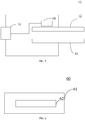
FIG. 1 is a schematic structural diagram illustrating a heat dissipation device according to an implementation of the present disclosure. -
FIG. 2 is a schematic structural diagram illustrating a heat dissipation device according to another implementation of the present disclosure. -
FIG. 3 is a schematic diagram illustrating a manner in which a first electric field is applied according to an implementation of the present disclosure. -
FIG. 4 is a schematic diagram illustrating a manner in which a second electric field is applied according to an implementation of the present disclosure. -
FIG. 5 is a schematic structural diagram illustrating a heat dissipation device according to yet another implementation of the present disclosure. -
FIG. 6 is a schematic structural diagram illustrating a terminal according to an implementation of the present disclosure. -
FIG. 7 is a schematic flowchart illustrating a method for controlling a heat dissipation device according to an implementation of the present disclosure. - A heat dissipation device with a simple structure and a small volume is provided in the present disclosure. As illustrated in
FIG. 1 , theheat dissipation device 10 includes a first conductive layer (also known as "electric conductive layer") 12, a secondconductive layer 14, and a powersupply control circuit 16. - The first
conductive layer 12 can be made of a thermal conductive material. In other words, the firstconductive layer 12 has not only conductive property but also thermal conductive property. The material of the firstconductive layer 12 can be any material with conductive property and thermal conductive property, which is not limited herein. As an example, the firstconductive layer 12 is a metal conductive layer. For example, the firstconductive layer 12 is a copper conductive layer or an aluminum conductive layer. In practice, the firstconductive layer 12 can be placed near a heat source of an apparatus to absorb heat generated by the heat source. - The material of the second
conductive layer 14 may be any material having conductive property, which is not limited herein. As an example, the material of the secondconductive layer 14 is metal, that is, the secondconductive layer 14 is a metal conductive layer. For example, the secondconductive layer 14 is a copper conductive layer or an aluminum conductive layer. In addition, in some implementations, the secondconductive layer 14 can also be made of a thermal conductive material, that is, the secondconductive layer 14 may have both conductive property and thermal conductive property. - The first
conductive layer 12 and the secondconductive layer 14 are disposed opposite to each other and may form a structure like a capacitor. For example, both the firstconductive layer 12 and the secondconductive layer 14 may have a plate-like structure, and one side of the firstconductive layer 12 is parallel to one side of the secondconductive layer 14. - The first
conductive layer 12 and the secondconductive layer 14 can be set apart from each other, such that an electric field can be created between the firstconductive layer 12 and the secondconductive layer 14. As an example, the firstconductive layer 12 is spaced apart from the secondconductive layer 14 via air. As another example, as illustrated inFIG. 2 , the firstconductive layer 12 is spaced apart from the secondconductive layer 14 via aninsulating layer 18. Theinsulating layer 18 can be made of any material with insulation characteristic. For example, theinsulating layer 18 is made of polymer (also known as " high-molecular polymer") materials. - The power
supply control circuit 16 can be coupled with the firstconductive layer 12 and the secondconductive layer 14. Thepower control circuit 16 is configured to alternately apply, between the firstconductive layer 12 and the secondconductive layer 14, a first electric field and a second electric field which are in opposite directions. - The structure of the power
supply control circuit 16 is not limited herein. As an example, the powersupply control circuit 16 includes a power supply, a control module, and a switch module. When the first electric field needs be applied between the firstconductive layer 12 and the secondconductive layer 14, the control module can couple the positive electrode of the power supply with the firstconductive layer 12 and couple the negative electrode of the power supply with the secondconductive layer 14 through the switch module, thereby forming an equivalent circuit as illustrated inFIG. 3 . When the second electric field needs to be applied between the firstconductive layer 12 and the secondconductive layer 14, the control module can change connection between the power supply and the firstconductive layer 12 as well as the secondconductive layer 14 through the switch module, such that the negative electrode of the power supply is coupled with the firstconductive layer 12 and the positive electrode of the power supply is coupled with the secondconductive layer 14, thereby forming an equivalent circuit as illustrated inFIG. 4 . - As another example, the power
supply control circuit 16 includes a first power supply, a second power supply, and a control module. The positive electrode of the first power supply is coupled with the firstconductive layer 12, and the negative electrode of the first power supply is coupled with the secondconductive layer 14. The negative electrode of the second power supply is coupled with the firstconductive layer 12, and the positive electrode of the second power supply is coupled with the secondconductive layer 14. When the first electric field needs to be applied between the firstconductive layer 12 and the secondconductive layer 14, the control module can control the first power supply to work, thereby forming the equivalent circuit as illustrated inFIG. 3 . When the second electric field needs to be applied between the firstconductive layer 12 and the secondconductive layer 14, the control module can control the second power supply to work, thereby forming the equivalent circuit as illustrated inFIG. 4 . - Working of the
heat dissipation device 10 will be described below with reference toFIGS. 3 and 4 . - First, in a narrow sense, temperature represents the intensity of the thermal motion of molecules.
- Assuming that the first
conductive layer 12 is near the heat source inside an apparatus, and the secondconductive layer 14 is away from the heat source, since the firstconductive layer 12 has thermal conductive property, the thermal motion of free electrons inside the firstconductive layer 12 is intensified under influence of the heat source. - When the first electric field illustrated in
FIG. 3 is applied between the firstconductive layer 12 and the secondconductive layer 14, under the action of the first electric field, free electrons with intense thermal motion in the firstconductive layer 12 are transferred to the secondconductive layer 14 via the power supply, and the direction of transfer of the free electrons is illustrated by an arrow inFIG. 3 . In contrast, thermal motion of internal molecules of the secondconductive layer 14 is slow, and the internal molecules interact (e.g., collide) with the free electrons with intense thermal motion from the firstconductive layer 12, which can reduce the intensity of the thermal motion of the free electrons from the firstconductive layer 12. - When the second electric field illustrated in
FIG. 4 is applied between the firstconductive layer 12 and the secondconductive layer 14, under the action of the second electric field, free electrons with low thermal motion in the secondconductive layer 14 are transferred to the firstconductive layer 12 via the power supply, and the direction of transfer of the free electrons is illustrated by an arrow inFIG. 4 . Since the thermal motion of the free electrons transferred from the secondconductive layer 14 to the firstconductive layer 12 is slow, internal molecules of the firstconductive layer 12 can interact with the these free electrons transferred from the secondconductive layer 14, which can reduce the intensity of the thermal motion of the internal molecules of the firstconductive layer 12. - The power
supply control circuit 16 alternately applies the first electric field and the second electric field between the firstconductive layer 12 and the secondconductive layer 14, whereby the free electrons with intense thermal motion in the firstconductive layer 12 can be transferred to the secondconductive layer 14, and the free electrons with low thermal motion in the secondconductive layer 14 can be transferred to the firstconductive layer 12. From an overall perspective, the heat of the firstconductive layer 12 is transferred to the secondconductive layer 14. - The
heat dissipation device 10 provided herein is configured to dissipate heat in an apparatus through active heat dissipation. With microscopic principle of temperature, theheat dissipation device 10 controls through the powersupply control circuit 16 the firstconductive layer 12 and the secondconductive layer 14 to exchange free electrons with different intensity of thermal motion, thereby achieving thermal conduction and heat dissipation. Unlike the conventional active heat dissipation, here, it is unnecessary to introduce a complicated system structure to theheat dissipation device 10, thus reducing the volume of theheat dissipation device 10. - The manner of controlling of the power
supply control circuit 16 is not limited herein. The following will provide several alternative control manners. - As an example, the power
supply control circuit 16 can be configured to perform the following alternately. Apply the first electric field between the firstconductive layer 12 and the secondconductive layer 14 until an electric field strength of the first electric field reaches a preset first threshold. Apply the second electric field between the firstconductive layer 12 and the secondconductive layer 14 until an electric field strength of the second electric field reaches a preset second threshold. For example, when the first electric field is applied, the powersupply control circuit 16 can monitor the electric field strength between the firstconductive layer 12 and the secondconductive layer 14. When the electric field strength between the firstconductive layer 12 and the secondconductive layer 14 reaches the preset first threshold, remove the first electric field, and then apply the second electric filed opposite to the first electric field between the firstconductive layer 12 and the secondconductive layer 14. When the second electric field is applied, the powersupply control circuit 16 can monitor the electric field strength between the firstconductive layer 12 and the secondconductive layer 14. When the electric field strength between the firstconductive layer 12 and the secondconductive layer 14 drops to the preset second threshold (the preset second threshold may be greater than or equal to zero), remove the second electric field and then apply the first electric field between the firstconductive layer 12 and the secondconductive layer 14. - As an example, the power
supply control circuit 16 can be configured to perform the following alternately. Apply the first electric field between the firstconductive layer 12 and the secondconductive layer 14 until a duration of the first electric field reaches a preset first duration. Apply the second electric field between the firstconductive layer 12 and the secondconductive layer 14 until a duration of the second electric field reaches a preset second duration. For example, when the first electric field is applied, the powersupply control circuit 16 can calculate the duration for which the first electric field is applied. When the duration of first electric field reaches the preset first duration, remove the first electric field and then apply the second electric filed opposite to the first electric field between the firstconductive layer 12 and the secondconductive layer 14. When the second electric field is applied, the powersupply control circuit 16 can monitor the duration for which the second electric field is applied. When the duration of the second electric field reaches the preset second duration, remove the second electric field and then apply the first electric field between the firstconductive layer 12 and the secondconductive layer 14. - A higher frequency of switching between the first electric field and the second electric field results in a higher speed of exchange of free electrons between the first
conductive layer 12 and the secondconductive layer 14 and a higher efficiency in thermal conduction between the firstconductive layer 12 and the secondconductive layer 14. The frequency of switching between the first electric field and the second electric field is not limited herein, and may be a fixed frequency or determined according to actual needs. - As an example, as illustrated in
FIG. 5 , theheat dissipation device 10 may further include a temperature measuring device 17. The temperature measuring device 17 can be configured to measure the temperature of the firstconductive layer 12. It should be understood that the temperature measuring device 17 can be in contact with the firstconductive layer 12 to measure the temperature of the firstconductive layer 12. Alternatively, the temperature measuring device 17 can be near the firstconductive layer 12, and air temperature around the firstconductive layer 12 can be taken as the temperature of the firstconductive layer 12. The powersupply control circuit 16 can be configured to control the frequency of switching between the first electric field and the second electric field according to the temperature of the firstconductive layer 12 measured by the temperature measuring device 17. As an example, the powersupply control circuit 16 can control the frequency of switching between the first electric field and the second electric field in a manner that a higher temperature of the firstconductive layer 12 leads to a higher frequency of switching between the first electric field and the second electric field. Specifically, the powersupply control circuit 16 may record a correspondence relationship between the temperature of the firstconductive layer 12 and the frequency of switching in advance, and the frequency of switching between the first electric field and the second electric field is set to the one corresponding to the current temperature of the firstconductive layer 12. - According to the implementations of the present disclosure, the frequency of switching between the first electric field and the second electric field is determined according to the temperature of the first
conductive layer 12, which improves the intelligence of the heat dissipation device. - A terminal is also provided. As illustrated in
FIG. 6 , the terminal 60 includes ahousing 61 and aheat dissipation device 62 received in thehousing 61. Theheat dissipation device 62 can be theheat dissipation device 10 described in any of the above implementations. - The terminal mentioned here may be, for example, a mobile terminal such as a "communication terminal" (or "terminal" for short), which can include but is not limited to a device configured via a wired line and/or a wireless interface to receive/transmit communication signals. Examples of the wired line may include, but are not limited to, at least one of a public switched telephone network (PSTN), a digital subscriber line (DSL), a digital cable, a direct connection cable, and/or another data connection line or network connection line. Examples of the wireless interface may include, but are not limited to, a wireless interface with a cellular network, a wireless local area network (WLAN), a digital television network (such as a digital video broadcasting-handheld (DVB-H) network), a satellite network, an amplitude modulation-frequency modulation (AM-FM) broadcast transmitter, and/or with another communication terminal. A communication terminal configured to communicate via a wireless interface may be called a "wireless communication terminal", a "wireless terminal", and/or a "mobile terminal". Examples of a mobile terminal may include, but are not limited to, a satellite or cellular telephone, a personal communication system (PCS) terminal capable of cellular radio telephone, data processing, fax, and/or data communication, a personal digital assistant (PDA) equipped with radio telephone, pager, Internet/Intranet access, web browsing, notebook, calendar, and/or global positioning system (GPS) receiver, and/or other electronic devices equipped with radio telephone capability such as a conventional laptop or a handheld receiver.
- The mobile terminal (such as a mobile phone) has small internal space and is difficult to accommodate an active heat dissipation system such as an air cooling system and a water cooling system, and thus a conventional mobile terminal usually adopts passive heat dissipation. In implementations of the present disclosure, the heat dissipation device capable of active heat dissipation is installed inside the mobile terminal, and the heat dissipation device has advantages of small volume and high heat dissipation efficiency and is very suitable for the mobile terminal.
- The heat dissipation device and the terminal provided herein are described in detail above with reference to
FIGS. 1-6 . Hereinafter, a method for controlling a heat dissipation device of implementations of the present disclosure will be described in detail with reference toFIG. 7 . The heat dissipation device may be anyheat dissipation device 10 described above. For description related to the heat dissipation device, reference can be made to the foregoing description, and repeated description will be properly omitted herein. - The heat dissipation device may include a first conductive layer and a second conductive layer disposed opposite to each other, and a power supply control circuit coupled with the first conductive layer and the second conductive layer. The first conductive layer is made of a thermal conductive material.
- The method illustrated in
FIG. 7 includes operations atblock 710. - At
block 710, the power supply control circuit applies, between the first conductive layer and the second conductive layer, a first electric field and a second electric field which are in opposite directions. - In some implementations, operations at
block 710 may include the following. The first electric field is applied between the first conductive layer and the second conductive layer until an electric field strength of the first electric field reaches a preset first threshold. The second electric field is applied between the first conductive layer and the second conductive layer until an electric field strength of the second electric field reaches a preset second threshold. - In some implementations, operations at
block 710 may include the following. The first electric field is applied between the first conductive layer and the second conductive layer until a duration of the first electric field reaches a preset first duration. The second electric field is applied between the first conductive layer and the second conductive layer until a duration of the second electric field reaches a preset second duration. - In some implementations, the heat dissipation device may further include a temperature measuring device configured to measure the temperature of the first
conductive layer 12. The method illustrated inFIG. 7 further includes that the power supply control circuit controls a frequency of switching between the first electric field and the second electric field according to the temperature of the first conductive layer measured by the temperature measuring device. - The above-mentioned implementations may be implemented, in whole or in part, in software, hardware, firmware, or any other combination thereof. When implemented in software, the implementations may be implemented, in whole or in part, in the form of a computer program product. The computer program product includes one or more computer instructions. When the computer program instructions are loaded and executed on a computer, procedures or functions described herein are generated in whole or in part. The computer can be a general-purpose computer, a special-purpose computer, a computer network, or other programmable devices. The computer instructions may be stored in a computer readable storage medium, or transmitted from one computer readable storage medium to another computer readable storage medium. For example, the computer instructions may be transmitted from one website, computer, server, or data center to another website site, computer, server, or data center in a wired manner or a wireless manner. Examples of the wired manner may include, but are not limited to a coaxial cable, an optical fiber, and a digital subscriber line (DSL). Examples of the wireless manner may include, but are not limited to infrared transmission, wireless transmission, and microwave transmission. The computer readable storage medium can be any usable medium that is accessible to the computer or a data storage device such as a server, data center, or other one or more usable media integrated devices. The usable medium may be a magnetic medium (for example, a floppy disk, a hard disk, a magnetic tape), an optical medium (such as a digital video disc (DVD)), or a semiconductor medium (such as a solid state disk (SSD)).
- Those of ordinary skill in the art will appreciate that, exemplary units and algorithm steps described in connection with the implementations disclosed herein can be implemented in electronic hardware, or in a combination of computer software and electronic hardware. Whether these functions are implemented in hardware or software depends on the specific application and design constraints of the technical solution. A professional technician could use different methods to implement the functions described herein for each particular application, but such implementations should not be considered to be beyond the scope of the present disclosure.
- It will be appreciated that the systems, devices, and methods disclosed in several implementations according to the present application may also be implemented in various other manners. For example, the above device implementations are merely illustrative, e.g., the division of units is only a division of logical functions, and there may exist other ways of division in practice, e.g., multiple units or components may be combined or may be integrated into another system, or some features may be ignored or not included. In other respects, the coupling or direct coupling or communication connection as illustrated or discussed may be an indirect coupling or communication connection through some interface, device or unit, and may be electrical, mechanical, or otherwise.
- Separated units as illustrated may or may not be physically separated. Components or parts displayed as units may or may not be physical units, and may reside at one location or may be distributed to multiple networked units. Some or all of the units may be selectively adopted according to practical needs to achieve desired objectives of the disclosure.
- Additionally, various functional units described in various implementations according to the present disclosure herein may be integrated into one processing unit or may be present as a number of physically separated units, and two or more units may be integrated into one.
- The above is only implementations of the present disclosure, and the scope of protection of the present disclosure is not limited thereto. Changes or substitutions that can be easily made by those skilled in the art without departing from the scope of the present disclosure shall be covered by the scope of protection of the present disclosure. The scope of protection of the disclosure shall be subject to the scope of protection of the appended claims.
Claims (13)
- A heat dissipation device, comprising:a first conductive layer and a second conductive layer disposed opposite to each other, and the first conductive layer being made of a thermal conductive material; anda power supply control circuit, coupled with the first conductive layer and the second conductive layer and configured to alternately apply, between the first conductive layer and the second conductive layer, a first electric field and a second electric field which are in opposite directions.
- The heat dissipation device of claim 1, further comprising:
an insulating layer, disposed between the first conductive layer and the second conductive layer. - The heat dissipation device of claim 2, wherein the insulating layer is made of a polymer material.
- The heat dissipation device of any of claims 1 to 3, wherein the power supply control circuit is configured to alternately:apply the first electric field between the first conductive layer and the second conductive layer until an electric field strength of the first electric field reaches a preset first threshold; andapply the second electric field between the first conductive layer and the second conductive layer until an electric field strength of the second electric field reaches a preset second threshold.
- The heat dissipation device of any of claims 1 to 3, wherein the power supply control circuit is configured to alternately:apply the first electric field between the first conductive layer and the second conductive layer until a duration of the first electric field reaches a preset first duration; andapply the second electric field between the first conductive layer and the second conductive layer until a duration of the second electric field reaches a preset second duration.
- The heat dissipation device of any of claims 1 to 5, further comprising:a temperature measuring device, configured to measure a temperature of the first conductive layer; andthe power supply control circuit being further configured to control a frequency of switching between the first electric field and the second electric field according to the temperature of the first conductive layer measured by the temperature measuring device.
- The heat dissipation device of any of claims 1 to 6, wherein at least one of the first conductive layer and the second conductive layer is a metal conductive layer.
- A terminal, comprising:a housing; andthe heat dissipation device of any of claims 1 to 7, the heat dissipation device being received in the housing.
- The terminal of claim 8, wherein the terminal is a mobile terminal.
- A method for controlling a heat dissipation device, the heat dissipation device comprising:a first conductive layer and a second conductive layer disposed opposite to each other, and the first conductive layer being made of a thermal conductive material; anda power supply control circuit, coupled with the first conductive layer and the second conductive layer;the method comprising:
applying alternately, by the power supply control circuit, a first electric field and a second electric field which are in opposite directions, between the first conductive layer and the second conductive layer. - The method of claim 10, wherein applying alternately the first electric field and the second electric field which are in opposite directions between the first conductive layer and the second conductive layer comprises:applying the first electric field between the first conductive layer and the second conductive layer until an electric field strength of the first electric field reaches a preset first threshold; andapplying the second electric field between the first conductive layer and the second conductive layer until an electric field strength of the second electric field reaches a preset second threshold.
- The method of claim 10, wherein applying alternately the first electric field and the second electric field which are in opposite directions between the first conductive layer and the second conductive layer comprises:applying the first electric field between the first conductive layer and the second conductive layer until a duration of the first electric field reaches a preset first duration; andapplying the second electric field between the first conductive layer and the second conductive layer until a duration of the second electric field reaches a preset second duration.
- The method of any of claims 10 to 12, wherein the heat dissipation device further comprises a temperature measuring device configured to measure a temperature of the first conductive layer;
the method further comprising:
controlling, by the power supply control circuit, a frequency of switching between the first electric field and the second electric field according to the temperature of the first conductive layer measured by the temperature measuring device.
Applications Claiming Priority (1)
| Application Number | Priority Date | Filing Date | Title |
|---|---|---|---|
| PCT/CN2017/107387 WO2019079953A1 (en) | 2017-10-23 | 2017-10-23 | Heat dissipation apparatus, terminal, and control method for heat dissipation apparatus |
Publications (2)
| Publication Number | Publication Date |
|---|---|
| EP3540335A1 true EP3540335A1 (en) | 2019-09-18 |
| EP3540335A4 EP3540335A4 (en) | 2020-02-12 |
Family
ID=66246145
Family Applications (1)
| Application Number | Title | Priority Date | Filing Date |
|---|---|---|---|
| EP17929627.2A Ceased EP3540335A4 (en) | 2017-10-23 | 2017-10-23 | HEAT DISSIPATION APPARATUS, TERMINAL AND CONTROL METHOD FOR HEAT DISSIPATION APPARATUS |
Country Status (6)
| Country | Link |
|---|---|
| US (1) | US20190269029A1 (en) |
| EP (1) | EP3540335A4 (en) |
| JP (1) | JP7189201B2 (en) |
| KR (1) | KR102318254B1 (en) |
| CN (1) | CN110140017B (en) |
| WO (1) | WO2019079953A1 (en) |
Families Citing this family (1)
| Publication number | Priority date | Publication date | Assignee | Title |
|---|---|---|---|---|
| KR102511597B1 (en) * | 2020-09-07 | 2023-03-17 | 주식회사 케이티앤지 | Aerosol generating apparatus and cartridge used for the same |
Family Cites Families (13)
| Publication number | Priority date | Publication date | Assignee | Title |
|---|---|---|---|---|
| US3415601A (en) * | 1965-07-14 | 1968-12-10 | Burroughs Corp | Magneto-carrier pressure motive force motor |
| US4136525A (en) * | 1976-12-30 | 1979-01-30 | International Business Machines Corporation | Dielectic refrigerator using orientable defect dipoles |
| JPH0810642B2 (en) * | 1988-11-07 | 1996-01-31 | 株式会社亜土電子工業 | PTC thermistor device |
| CN1076809A (en) * | 1992-10-29 | 1993-09-29 | 科尔涅伊·D·托夫斯蒂尤克 | Capacitive thermoelectric device |
| JP2000243546A (en) | 1999-02-18 | 2000-09-08 | Nissan Motor Co Ltd | Heating device, heating method and flow meter |
| CN100477312C (en) * | 2003-01-30 | 2009-04-08 | 松下电器产业株式会社 | Thermal switching element and method for manufacturing the same |
| US8371128B2 (en) * | 2009-11-17 | 2013-02-12 | Empire Technology Development, Llc | Thermal management with electrocaloric effect layer |
| US8695353B2 (en) * | 2009-12-17 | 2014-04-15 | Empire Technology Development Llc | Electrocaloric cooling |
| US20110168378A1 (en) * | 2010-01-14 | 2011-07-14 | Irvine Sensors Corporation | Thermal power distribution system |
| US9157669B2 (en) | 2011-04-20 | 2015-10-13 | Empire Technology Development Llc | Heterogeneous electrocaloric effect heat transfer device |
| CN102244049A (en) * | 2011-06-29 | 2011-11-16 | 鸿富锦精密工业(深圳)有限公司 | Circuit board assembly and heat radiation structure thereof |
| US9109818B2 (en) * | 2013-09-20 | 2015-08-18 | Palo Alto Research Center Incorporated | Electrocaloric cooler and heat pump |
| CN105792619A (en) * | 2016-04-29 | 2016-07-20 | 广东欧珀移动通信有限公司 | Heat sink and mobile terminal |
-
2017
- 2017-10-23 KR KR1020207004501A patent/KR102318254B1/en not_active Expired - Fee Related
- 2017-10-23 EP EP17929627.2A patent/EP3540335A4/en not_active Ceased
- 2017-10-23 WO PCT/CN2017/107387 patent/WO2019079953A1/en not_active Ceased
- 2017-10-23 JP JP2020509513A patent/JP7189201B2/en active Active
- 2017-10-23 CN CN201780063127.XA patent/CN110140017B/en not_active Expired - Fee Related
-
2019
- 2019-05-07 US US16/405,152 patent/US20190269029A1/en not_active Abandoned
Also Published As
| Publication number | Publication date |
|---|---|
| US20190269029A1 (en) | 2019-08-29 |
| WO2019079953A1 (en) | 2019-05-02 |
| KR20200031654A (en) | 2020-03-24 |
| CN110140017A (en) | 2019-08-16 |
| JP2020532116A (en) | 2020-11-05 |
| KR102318254B1 (en) | 2021-10-27 |
| CN110140017B (en) | 2021-08-31 |
| EP3540335A4 (en) | 2020-02-12 |
| JP7189201B2 (en) | 2022-12-13 |
Similar Documents
| Publication | Publication Date | Title |
|---|---|---|
| US11122710B2 (en) | Heat dissipation structure for electronic device and electronic device | |
| US20170118865A1 (en) | Mobile terminal and heat sink thereof | |
| CN110167322A (en) | Shell and electronic equipment | |
| US12547225B2 (en) | Method and apparatus for an enclosed ionic thermal module | |
| CN102832890A (en) | Radio frequency low-temperature low-noise amplifier system of thermoelectric refrigeration | |
| US11812583B2 (en) | Passive thermal-control system of a mesh network device and associated mesh network devices | |
| CN105611126A (en) | Camera heat dissipation structure and mobile terminal | |
| WO2023133362A1 (en) | System and method for a 5g cooling module that directs heat into a thermal loop associated with a processing device | |
| US20190269029A1 (en) | Heat Dissipation Device and Control Method Thereof, Terminal | |
| US20170290194A1 (en) | Thermal modulation of an electronic device | |
| US9099769B2 (en) | Antenna mechanical faceplate design | |
| KR20160001403U (en) | Electronic device thermal management system | |
| HK40009071B (en) | Heat dissipation apparatus, terminal, and control method for heat dissipation apparatus | |
| US20180310360A1 (en) | Wearable wireless access point | |
| HK40009071A (en) | Heat dissipation apparatus, terminal, and control method for heat dissipation apparatus | |
| CN214378862U (en) | Antenna systems and electronic equipment | |
| CN114171879B (en) | Heat dissipation structure, satellite communication device and vehicle | |
| CN113192679B (en) | Coaxial cable and electronic equipment | |
| CN211267233U (en) | Novel circuit board assembly with electronic device protection function | |
| CN215990827U (en) | Wireless signal shielding device module and full-band wireless signal shielding device | |
| US10594015B2 (en) | Dual purpose heat pipe and antenna apparatus | |
| US9414528B2 (en) | Thermal spreading for an externally pluggable electronic module | |
| CN210275024U (en) | Heat conduction shielding body | |
| CN210091010U (en) | Computer mainboard suitable for harsh application environment | |
| CN113904403A (en) | Charging seat, charging seat adjusting method and electronic equipment |
Legal Events
| Date | Code | Title | Description |
|---|---|---|---|
| STAA | Information on the status of an ep patent application or granted ep patent |
Free format text: STATUS: THE INTERNATIONAL PUBLICATION HAS BEEN MADE |
|
| PUAI | Public reference made under article 153(3) epc to a published international application that has entered the european phase |
Free format text: ORIGINAL CODE: 0009012 |
|
| STAA | Information on the status of an ep patent application or granted ep patent |
Free format text: STATUS: REQUEST FOR EXAMINATION WAS MADE |
|
| 17P | Request for examination filed |
Effective date: 20190612 |
|
| AK | Designated contracting states |
Kind code of ref document: A1 Designated state(s): AL AT BE BG CH CY CZ DE DK EE ES FI FR GB GR HR HU IE IS IT LI LT LU LV MC MK MT NL NO PL PT RO RS SE SI SK SM TR |
|
| AX | Request for extension of the european patent |
Extension state: BA ME |
|
| RAP1 | Party data changed (applicant data changed or rights of an application transferred) |
Owner name: GUANGDONG OPPO MOBILE TELECOMMUNICATIONS CORP., LT |
|
| A4 | Supplementary search report drawn up and despatched |
Effective date: 20200114 |
|
| RIC1 | Information provided on ipc code assigned before grant |
Ipc: F25B 21/00 20060101AFI20200108BHEP |
|
| STAA | Information on the status of an ep patent application or granted ep patent |
Free format text: STATUS: EXAMINATION IS IN PROGRESS |
|
| 17Q | First examination report despatched |
Effective date: 20200730 |
|
| DAV | Request for validation of the european patent (deleted) | ||
| DAX | Request for extension of the european patent (deleted) | ||
| APBK | Appeal reference recorded |
Free format text: ORIGINAL CODE: EPIDOSNREFNE |
|
| APBN | Date of receipt of notice of appeal recorded |
Free format text: ORIGINAL CODE: EPIDOSNNOA2E |
|
| APBR | Date of receipt of statement of grounds of appeal recorded |
Free format text: ORIGINAL CODE: EPIDOSNNOA3E |
|
| APAF | Appeal reference modified |
Free format text: ORIGINAL CODE: EPIDOSCREFNE |
|
| REG | Reference to a national code |
Ref country code: DE Ref legal event code: R003 |
|
| APBT | Appeal procedure closed |
Free format text: ORIGINAL CODE: EPIDOSNNOA9E |
|
| STAA | Information on the status of an ep patent application or granted ep patent |
Free format text: STATUS: THE APPLICATION HAS BEEN REFUSED |
|
| 18R | Application refused |
Effective date: 20230420 |