EP3538840B1 - Method and system for multiple f-number lens - Google Patents
Method and system for multiple f-number lens Download PDFInfo
- Publication number
- EP3538840B1 EP3538840B1 EP17869247.1A EP17869247A EP3538840B1 EP 3538840 B1 EP3538840 B1 EP 3538840B1 EP 17869247 A EP17869247 A EP 17869247A EP 3538840 B1 EP3538840 B1 EP 3538840B1
- Authority
- EP
- European Patent Office
- Prior art keywords
- light
- nir
- wavelength range
- region
- pixels
- Prior art date
- Legal status (The legal status is an assumption and is not a legal conclusion. Google has not performed a legal analysis and makes no representation as to the accuracy of the status listed.)
- Active
Links
Images


Classifications
-
- G—PHYSICS
- G01—MEASURING; TESTING
- G01S—RADIO DIRECTION-FINDING; RADIO NAVIGATION; DETERMINING DISTANCE OR VELOCITY BY USE OF RADIO WAVES; LOCATING OR PRESENCE-DETECTING BY USE OF THE REFLECTION OR RERADIATION OF RADIO WAVES; ANALOGOUS ARRANGEMENTS USING OTHER WAVES
- G01S17/00—Systems using the reflection or reradiation of electromagnetic waves other than radio waves, e.g. lidar systems
- G01S17/02—Systems using the reflection of electromagnetic waves other than radio waves
- G01S17/06—Systems determining position data of a target
- G01S17/42—Simultaneous measurement of distance and other co-ordinates
-
- G—PHYSICS
- G01—MEASURING; TESTING
- G01S—RADIO DIRECTION-FINDING; RADIO NAVIGATION; DETERMINING DISTANCE OR VELOCITY BY USE OF RADIO WAVES; LOCATING OR PRESENCE-DETECTING BY USE OF THE REFLECTION OR RERADIATION OF RADIO WAVES; ANALOGOUS ARRANGEMENTS USING OTHER WAVES
- G01S17/00—Systems using the reflection or reradiation of electromagnetic waves other than radio waves, e.g. lidar systems
- G01S17/88—Lidar systems specially adapted for specific applications
- G01S17/89—Lidar systems specially adapted for specific applications for mapping or imaging
- G01S17/894—3D imaging with simultaneous measurement of time-of-flight at a 2D array of receiver pixels, e.g. time-of-flight cameras or flash lidar
-
- G—PHYSICS
- G01—MEASURING; TESTING
- G01S—RADIO DIRECTION-FINDING; RADIO NAVIGATION; DETERMINING DISTANCE OR VELOCITY BY USE OF RADIO WAVES; LOCATING OR PRESENCE-DETECTING BY USE OF THE REFLECTION OR RERADIATION OF RADIO WAVES; ANALOGOUS ARRANGEMENTS USING OTHER WAVES
- G01S7/00—Details of systems according to groups G01S13/00, G01S15/00, G01S17/00
- G01S7/48—Details of systems according to groups G01S13/00, G01S15/00, G01S17/00 of systems according to group G01S17/00
- G01S7/481—Constructional features, e.g. arrangements of optical elements
- G01S7/4816—Constructional features, e.g. arrangements of optical elements of receivers alone
-
- G—PHYSICS
- G01—MEASURING; TESTING
- G01S—RADIO DIRECTION-FINDING; RADIO NAVIGATION; DETERMINING DISTANCE OR VELOCITY BY USE OF RADIO WAVES; LOCATING OR PRESENCE-DETECTING BY USE OF THE REFLECTION OR RERADIATION OF RADIO WAVES; ANALOGOUS ARRANGEMENTS USING OTHER WAVES
- G01S7/00—Details of systems according to groups G01S13/00, G01S15/00, G01S17/00
- G01S7/48—Details of systems according to groups G01S13/00, G01S15/00, G01S17/00 of systems according to group G01S17/00
- G01S7/483—Details of pulse systems
- G01S7/486—Receivers
- G01S7/4865—Time delay measurement, e.g. time-of-flight measurement, time of arrival measurement or determining the exact position of a peak
-
- G—PHYSICS
- G02—OPTICS
- G02B—OPTICAL ELEMENTS, SYSTEMS OR APPARATUS
- G02B13/00—Optical objectives specially designed for the purposes specified below
- G02B13/14—Optical objectives specially designed for the purposes specified below for use with infrared or ultraviolet radiation
-
- G—PHYSICS
- G02—OPTICS
- G02B—OPTICAL ELEMENTS, SYSTEMS OR APPARATUS
- G02B27/00—Optical systems or apparatus not provided for by any of the groups G02B1/00 - G02B26/00, G02B30/00
- G02B27/0093—Optical systems or apparatus not provided for by any of the groups G02B1/00 - G02B26/00, G02B30/00 with means for monitoring data relating to the user, e.g. head-tracking, eye-tracking
-
- G—PHYSICS
- G02—OPTICS
- G02B—OPTICAL ELEMENTS, SYSTEMS OR APPARATUS
- G02B27/00—Optical systems or apparatus not provided for by any of the groups G02B1/00 - G02B26/00, G02B30/00
- G02B27/10—Beam splitting or combining systems
- G02B27/1006—Beam splitting or combining systems for splitting or combining different wavelengths
-
- G—PHYSICS
- G02—OPTICS
- G02B—OPTICAL ELEMENTS, SYSTEMS OR APPARATUS
- G02B27/00—Optical systems or apparatus not provided for by any of the groups G02B1/00 - G02B26/00, G02B30/00
- G02B27/10—Beam splitting or combining systems
- G02B27/14—Beam splitting or combining systems operating by reflection only
- G02B27/141—Beam splitting or combining systems operating by reflection only using dichroic mirrors
-
- G—PHYSICS
- G02—OPTICS
- G02B—OPTICAL ELEMENTS, SYSTEMS OR APPARATUS
- G02B5/00—Optical elements other than lenses
- G02B5/20—Filters
- G02B5/208—Filters for use with infrared or ultraviolet radiation, e.g. for separating visible light from infrared and/or ultraviolet radiation
-
- G—PHYSICS
- G06—COMPUTING OR CALCULATING; COUNTING
- G06T—IMAGE DATA PROCESSING OR GENERATION, IN GENERAL
- G06T7/00—Image analysis
- G06T7/50—Depth or shape recovery
- G06T7/521—Depth or shape recovery from laser ranging, e.g. using interferometry; from the projection of structured light
-
- H—ELECTRICITY
- H04—ELECTRIC COMMUNICATION TECHNIQUE
- H04N—PICTORIAL COMMUNICATION, e.g. TELEVISION
- H04N13/00—Stereoscopic video systems; Multi-view video systems; Details thereof
- H04N13/20—Image signal generators
- H04N13/204—Image signal generators using stereoscopic image cameras
- H04N13/254—Image signal generators using stereoscopic image cameras in combination with electromagnetic radiation sources for illuminating objects
-
- H—ELECTRICITY
- H04—ELECTRIC COMMUNICATION TECHNIQUE
- H04N—PICTORIAL COMMUNICATION, e.g. TELEVISION
- H04N13/00—Stereoscopic video systems; Multi-view video systems; Details thereof
- H04N13/30—Image reproducers
- H04N13/332—Displays for viewing with the aid of special glasses or head-mounted displays [HMD]
-
- H—ELECTRICITY
- H04—ELECTRIC COMMUNICATION TECHNIQUE
- H04N—PICTORIAL COMMUNICATION, e.g. TELEVISION
- H04N13/00—Stereoscopic video systems; Multi-view video systems; Details thereof
- H04N13/30—Image reproducers
- H04N13/366—Image reproducers using viewer tracking
- H04N13/383—Image reproducers using viewer tracking for tracking with gaze detection, i.e. detecting the lines of sight of the viewer's eyes
-
- H—ELECTRICITY
- H04—ELECTRIC COMMUNICATION TECHNIQUE
- H04N—PICTORIAL COMMUNICATION, e.g. TELEVISION
- H04N23/00—Cameras or camera modules comprising electronic image sensors; Control thereof
- H04N23/50—Constructional details
- H04N23/55—Optical parts specially adapted for electronic image sensors; Mounting thereof
-
- H—ELECTRICITY
- H04—ELECTRIC COMMUNICATION TECHNIQUE
- H04N—PICTORIAL COMMUNICATION, e.g. TELEVISION
- H04N23/00—Cameras or camera modules comprising electronic image sensors; Control thereof
- H04N23/56—Cameras or camera modules comprising electronic image sensors; Control thereof provided with illuminating means
-
- H—ELECTRICITY
- H04—ELECTRIC COMMUNICATION TECHNIQUE
- H04N—PICTORIAL COMMUNICATION, e.g. TELEVISION
- H04N23/00—Cameras or camera modules comprising electronic image sensors; Control thereof
- H04N23/60—Control of cameras or camera modules
- H04N23/667—Camera operation mode switching, e.g. between still and video, sport and normal or high- and low-resolution modes
-
- H—ELECTRICITY
- H04—ELECTRIC COMMUNICATION TECHNIQUE
- H04N—PICTORIAL COMMUNICATION, e.g. TELEVISION
- H04N23/00—Cameras or camera modules comprising electronic image sensors; Control thereof
- H04N23/60—Control of cameras or camera modules
- H04N23/67—Focus control based on electronic image sensor signals
- H04N23/671—Focus control based on electronic image sensor signals in combination with active ranging signals, e.g. using light or sound signals emitted toward objects
-
- H—ELECTRICITY
- H04—ELECTRIC COMMUNICATION TECHNIQUE
- H04N—PICTORIAL COMMUNICATION, e.g. TELEVISION
- H04N23/00—Cameras or camera modules comprising electronic image sensors; Control thereof
- H04N23/70—Circuitry for compensating brightness variation in the scene
- H04N23/71—Circuitry for evaluating the brightness variation
-
- H—ELECTRICITY
- H04—ELECTRIC COMMUNICATION TECHNIQUE
- H04N—PICTORIAL COMMUNICATION, e.g. TELEVISION
- H04N23/00—Cameras or camera modules comprising electronic image sensors; Control thereof
- H04N23/70—Circuitry for compensating brightness variation in the scene
- H04N23/75—Circuitry for compensating brightness variation in the scene by influencing optical camera components
-
- H—ELECTRICITY
- H04—ELECTRIC COMMUNICATION TECHNIQUE
- H04N—PICTORIAL COMMUNICATION, e.g. TELEVISION
- H04N25/00—Circuitry of solid-state image sensors [SSIS]; Control thereof
- H04N25/20—Circuitry of solid-state image sensors [SSIS]; Control thereof for transforming only infrared radiation into image signals
-
- H—ELECTRICITY
- H04—ELECTRIC COMMUNICATION TECHNIQUE
- H04N—PICTORIAL COMMUNICATION, e.g. TELEVISION
- H04N25/00—Circuitry of solid-state image sensors [SSIS]; Control thereof
- H04N25/40—Extracting pixel data from image sensors by controlling scanning circuits, e.g. by modifying the number of pixels sampled or to be sampled
- H04N25/42—Extracting pixel data from image sensors by controlling scanning circuits, e.g. by modifying the number of pixels sampled or to be sampled by switching between different modes of operation using different resolutions or aspect ratios, e.g. switching between interlaced and non-interlaced mode
-
- H—ELECTRICITY
- H04—ELECTRIC COMMUNICATION TECHNIQUE
- H04N—PICTORIAL COMMUNICATION, e.g. TELEVISION
- H04N25/00—Circuitry of solid-state image sensors [SSIS]; Control thereof
- H04N25/40—Extracting pixel data from image sensors by controlling scanning circuits, e.g. by modifying the number of pixels sampled or to be sampled
- H04N25/46—Extracting pixel data from image sensors by controlling scanning circuits, e.g. by modifying the number of pixels sampled or to be sampled by combining or binning pixels
-
- G—PHYSICS
- G02—OPTICS
- G02B—OPTICAL ELEMENTS, SYSTEMS OR APPARATUS
- G02B1/00—Optical elements characterised by the material of which they are made; Optical coatings for optical elements
- G02B1/10—Optical coatings produced by application to, or surface treatment of, optical elements
- G02B1/11—Anti-reflection coatings
-
- G—PHYSICS
- G02—OPTICS
- G02B—OPTICAL ELEMENTS, SYSTEMS OR APPARATUS
- G02B27/00—Optical systems or apparatus not provided for by any of the groups G02B1/00 - G02B26/00, G02B30/00
- G02B27/30—Collimators
Definitions
- imaging lenses are utilized to collimate light, focus light, and the like.
- focus light and the like.
- imaging lenses are utilized to collimate light, focus light, and the like.
- the present invention relates to the imaging systems and methods as claimed.
- embodiments of the present invention provide an imaging lens that may be characterized by a lower f-number for NIR light and a higher f-number for visible light by utilizing a wavelength-selective filter at its aperture stop.
- embodiments of the present invention provide an image sensor that may be operated at a lower resolution mode for NIR light using pixel binning and at a higher resolution mode for visible light using native pixel resolution.
- the imaging lens and the image sensor may be suitable for use as a TOF depth sensor with active illumination in the NIR wavelength range where a faster lens and more light integration are desired, as well as a computer vision sensor with passive illumination in the visible wavelength range where higher image resolution and greater depth of field are desired.
- the imaging lens may be suitable for use for both imaging visible light at a lower photo speed and imaging IR light at a faster photo speed.
- the present invention relates generally to imaging systems with a multiple f-number lens.
- the f-number (sometimes referred to as the focal ratio, f-ratio, f-stop, or relative aperture) of a lens is the ratio of the lens's focal length to the diameter of the entrance pupil.
- the f-number is a dimensionless number that is a quantitative measure of lens speed.
- a higher f-number implies a smaller diameter stop for a given focal-length lens.
- the exposure time would need to be four times as long, or alternatively, the illumination would need to be increased to a level four times as high as the original level.
- Increasing the f-number may have the benefit of increasing the depth of field (DoF) and increasing the spatial resolution of an image (e.g., as measured by modulation transfer function or MTF).
- DoF depth of field
- MTF modulation transfer function
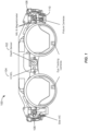
- FIG. 1 illustrates schematically a system 100 that includes an imaging system 102 and an illumination source 104 according to an embodiment of the present invention.
- the system 100 may be integrated in a goggle, as illustrated in FIG. 1 , that can be worn by a user for virtual reality (VR) or augmented reality (AR) experiences.
- the system 100 may include other optical and electronic components for creating VR and AR experiences.
- the imaging system 102 and the illumination source 104 may be used for time-of-flight (TOF) depth sensing.
- the illumination source 104 can be configured to emit a plurality of laser pulses. A portion of each of the plurality of laser pulses may be reflected off of an object in front of the user. The portion of each of the plurality of laser pulses reflected off of one or more objects may be received and imaged by the imaging system 102.
- the imaging system 102 can be configured to determine a time of flight for each of the laser pulses from emission to detection, thereby determining the distance of the object from the user.
- the illumination source 104 may comprise a laser source, such as a vertical-cavity surface-emitting laser (VCSEL).
- VCSEL vertical-cavity surface-emitting laser
- the laser source may be configured to emit laser pulses in the near infrared (NIR) wavelength range, for example in the wavelength range from about 750 nm to about 1400 nm.
- the illumination source 104 may also include a collimation lens for collimating the plurality of laser pulses.
- the imaging system 102 may also be used for computer vision.
- the imaging system 102 is configured to image objects in front of the user that are illuminated by passive ambient light in the visible wavelength range.
- the imaging system 102 may be used in other systems.
- the world cameras (WC) 106 and 108, as well as the picture camera 110 may also be configured for dual functions, i.e., for imaging both visible and infrared light.
- the system 100 may operate the imaging system 102 in a time-shared fashion such that depth sensing and computer vision are alternately performed at different time slots.
- the duration of each time slot may range from about 1 ms to about 50 ms, so that there is no significant latency in either depth sensing or computer vision.
- the system 100 may operate the imaging system 102 to perform depth sensing and computer vision simultaneously, as described in more detailed below.
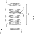
- FIG. 2 illustrates schematically an imaging system 200 that may be used for dual-wavelength sensing according to some embodiments of the present invention.
- the imaging system 200 may be used for both TOF depth sensing in the NIR wavelength range and computer vision in the visible wavelength range.
- the imaging system 200 includes an imaging lens 210 and an image sensor 220 positioned at an image plane of the imaging lens 210.
- the imaging lens 210 may include one or more lens elements 216a-216e disposed along an optical axis.
- the imaging lens may further include an aperture stop 212 that may define the entrance pupil size. In a lens system, the limiting diameter that determines the amount of light that reaches the image is called the aperture stop.
- the aperture stop may be positioned near the front of a compound imaging lens.
- the aperture stop may be positioned between two groups of lens elements of a compound imaging lens (e.g., as illustrated in FIG. 2 ).
- the entrance pupil size is determined by the image of the aperture stop formed by the lens elements preceding the aperture stop. In the following, it is assumed that the entrance pupil size is the same as the aperture stop size.
- the imaging lens 210 When the imaging system 200 is used for TOF depth sensing, it may be advantageous to configure the imaging lens 210 as a fast lens so that a relatively low power laser source may be used for active illumination. Lower power illumination may lead to lower cost, smaller form factor, and lower power consumption, among other advantages. In some cases, a relatively low f /#, for example in a range from about f /1 to about f /1.4, may be desirable for TOF depth sensing. In contrast, when the imaging system 200 is used for computer vision, it may be advantageous to configure the imaging lens 210 as a slow lens so that higher spatial resolution and greater depth of field (DoF) may be achieved.
- DoF depth of field
- a relatively high f /# for example in a range from about f /2 to about f /2.8, may be desirable for computer vision.
- the imaging system 200 may be applied to other applications where it may be desirable to have different lens speeds for sensing light in different wavelength ranges (e.g., for infrared sensing and visible light sensing).
- the imaging lens 210 includes a filter 214 positioned at the aperture stop 212 that functions as a wavelength selective filter.
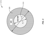
- FIG. 3 shows a schematic plan view of a filter 214 that is used in the imaging lens 210 according to an embodiment of the present invention.
- the filter 214 includes two regions: a central (e.g., circular) region 310 with a first diameter D 1 , and an outer (e.g., annular) region 320 surrounding the central region 310.
- the outer region 320 is characterized by a second diameter D 2 as its outer diameter.
- the second diameter D 2 may be substantially the same as the diameter of the aperture stop 212.
- the central region 310 is depicted as having a circular shape in FIG. 3 , other shapes, such as elliptical, square, rectangular shapes can also be used.
- the outer region 320 is depicted as having an annular shape in FIG. 3 , other shapes are also possible.
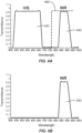
- FIG. 4A is a plot of an exemplary transmittance curve as a function of wavelength for the central region 310 of the filter 214 according to an embodiment of the present invention.
- FIG. 4B is a plot of an exemplary transmittance curve as a function of wavelength for the outer region 320 of the filter 214 according to an embodiment of the present invention.
- the central region 310 of the filter 214 is configured to have a first transmission band 430 in the NIR wavelength range (e.g., from about 800 nm to about 950 nm) and a second transmission band 440 in the visible (VIS) wavelength range (e.g., from about 400 nm to about 700 nm).
- VIS visible
- the central region 310 is characterized by high transmittance values in both the NIR and the visible wavelength ranges.
- the outer region 320 is configured to have only one transmission band 450 in the NIR wavelength range (e.g., from about 800 nm to about 950 nm), such that the outer region 320 is characterized by high transmittance values in the NIR wavelength range but low transmittance values in the visible wavelength range.
- the filter 214 may comprise a multilayer thin film stack formed on a surface of a transparent substrate such as glass.
- a multilayer thin film may comprise a periodic layer system composed from two or more materials of differing indices of refraction. This periodic system may be engineered to significantly enhance the transmittance of the surface in one or more desired wavelength ranges, while suppressing the transmittance of the surface in other wavelength ranges. The maximum transmittance may be increased up to nearly 100% with increasing number of layers in the stack.
- the thicknesses of the layers making up the multilayer thin film stack are generally quarter-wave, designed such that transmitted beams constructively interfere with one another to maximize transmission and minimize reflection.
- the multilayer thin film stack in the central region 310 may be engineered to have two high transmittance bands, one in the visible wavelength range and the other in the NIR wavelength range, and have low transmittance for all other wavelengths.
- the multilayer thin film stack in the annular region 320 may be engineered to have only one high transmittance band in the NIR wavelength range, and have low transmittance for all other wavelengths.
- other types of bandpass filters such as metasurface filter, may be used.
- FIG. 5 illustrates a schematic cross-sectional view of a wavelength-selective filter 500 according to some embodiments of the present invention.
- the filter 500 may include a transparent substrate 502 such as a piece of glass, a first multilayer thin film 510 disposed on a front surface of the substrate 502, and a second multilayer thin film 520 disposed on the first multilayer thin film 510.
- the first multilayer thin film 510 may have a circular shape with a diameter D 2 .
- the second multilayer thin film 520 may have an annular shape with an inner diameter D 1 and an outer diameter D 2 .
- the filter 500 may further include an anti-reflective coating 530 on the back surface of the substrate 502.
- the first multilayer thin film 510 may be configured to have a transmittance curve that exhibits a first transmission band 430 in the NIR wavelength range (e.g., about 800 nm to about 950 nm) and a second transmission band 440 in the visible (VIS) wavelength range (e.g., about 400 nm to about 700 nm), as illustrated in FIG. 4A .
- the second multilayer thin film 520 may be configured as a high-pass filter that transmits light in the NIR wavelength range and blocks light in the visible wavelength range, as illustrated by the dashed curve 460 in FIG. 4A .
- the combination of the first multilayer thin film 510 and the second multilayer thin film 520 may result in an effective transmittance curve 450 as illustrated in FIG. 4B for the outer region of the filter 500.
- the outer region of the filter 500 may effectively transmit only light in the NIR wavelength range, while the central region of the filter 500 may transmit light in both visible and NIR wavelength ranges.
- the filter 214 or 500 may effectively give rise to two different apertures for the imaging lens 210 depending on the wavelength range of the light being imaged.
- the imaging lens 210 is used for imaging NIR light, for example for TOF depth sensing where the illumination laser source 104 (as illustrated in FIG. 1 ) operates in the NIR wavelength range
- the NIR light is transmitted through both the central region 310 and the outer region 320 of the filter 214.
- the effective aperture of the imaging lens 210 for NIR light is the second diameter D 2 .
- the imaging lens 210 When the imaging lens 210 is used for imaging visible light, for example for computer vision where the illumination is from the ambient visible light, the visible light is transmitted only through the central region 310. Thus, the effective aperture of the imaging lens 210 for visible light is the first diameter D 1 .
- the imaging lens 210 with the wavelength-selective filter 214 may be applied to other applications where it may be desirable to have different lens speeds for sensing light in different wavelength ranges.
- the imaging lens 210 has a focal length f .
- the imaging lens 210 can be configured to have a relatively low f / # NIR for TOF depth sensing in the NIR wavelength range, and a relatively high f / # VIS for computer vision in the visible wavelength range.
- a lower f /# means that more active illumination NIR light can pass through the imaging lens 210. Therefore a relatively low power laser source may be used for illumination, which may lead to lower cost, smaller form factor, and lower power consumption, among other advantages.
- the value of D 2 may be chosen such that f / # NIR is in a range from about f /1 to about f /1.4.
- a higher f /# may afford higher spatial resolution at the image plane (e.g., as measured by MTF) and greater DoF, among other advantages.
- a lower f /# may not be desired when imaging visible light in some cases.
- image sensors typically have higher quantum efficiencies in the visible wavelength range than in the NIR wavelength range.
- the image sensor may be saturated when a fast lens is used for imaging visible light.
- the value of D 1 may be chosen such that f / # VIS is in a range from about f /2 to about f /2.8.
- the intensity ratio between VIS and NIR modes can be controlled by setting the ratio D 1 /D 2 accordingly.
- a ratio of D 1 /D 2 may be chosen to be in the range from about 0.4 to about 0.6. In one embodiment the ratio of D 1 /D 2 may be chosen to be about 0.5, so that the value of f / # VIS is about twice as large as the value of f l# NIR .
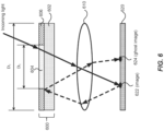
- FIG. 6 illustrates a schematic imaging system according to some embodiments.
- the imaging system includes a wavelength-selective filter 600, an optical lens 610, and an image sensor 620. Although a single lens element is depicted for the optical lens 610 in FIG. 6 for simplicity of illustration, the optical lens 610 may include several lens elements.
- the filter 600 may include a transparent substrate 602 such as a piece of glass, a first multilayer thin film 604 that has a circular shape with a first diameter D 1 , and a second multilayer thin film 606 that has an annular shape surrounding the first multilayer thin film 604 with an outer diameter of D 2 .
- the first multilayer thin film 604 may be configured to have high transmittance for both the visible and NIR wavelength ranges, and the second multilayer thin film 606 may be configured to have high transmittance for only the NIR wavelength range, as discussed above.
- an incoming light ray in the visible wavelength range may be transmitted by the first multilayer thin film 604 and form an image spot 622 at the image sensor, as illustrated by the light path represented by the solid arrows.
- a portion of the incoming light may be reflected by the image sensor 620 and incident on a back side of the second multilayer film 606, as illustrated by the light path represented by the dashed arrows.
- the reflected light may be reflected by the second multilayer thin film 606, as the second multilayer thin film 606 is configured to have low transmittance values and high reflectance values in the visible wavelength range.
- the light reflected by the second multilayer thin film 606 may form a ghost image 624 at the image sensor 620.
- the filter 600 may not present a significant ghost image problem for light in the NIR wavelength range.
- FIG. 7 shows a ray tracing diagram of an exemplary imaging system for a field point (e.g., collimated rays at a certain incidence angle) according to some embodiments.
- the image system may include a wavelength-selective filter 700, an optical lens 710, and an image sensor 720.
- FIG. 8 shows intensity distributions at the image sensor 720 as simulated by the ray tracing. As illustrated, the intensity distributions show an image point 810, as well as a ghost image 820. The ghost image may obscure the real image. Therefore, it may be desirable to prevent the formation of the ghost image.
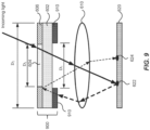
- FIG. 9 illustrates a schematic cross-sectional diagram of a wavelength-selective filter 900 that may be used in an imaging system and may prevent ghost image formation according to some embodiments.
- the filter 900 includes a transparent substrate 602, a first multilayer thin film 604 formed on a front side of the substrate 602 having a circular shape with a first diameter D 1 , and a second multilayer thin film 606 formed on the front side of the substrate 602 having an annular shape surrounding the first multilayer thin film 604 with an outer diameter of D 2 .
- the first multilayer thin film 604 may be configured to have high transmittance values in both the visible and NIR wavelength ranges
- the second multilayer thin film 606 may be configured to have high transmittance values in only the NIR wavelength range, as discussed above.
- the filter 900 may further include a third thin film 910 formed on a back side of the substrate 602.
- the third thin film 910 may have an annular shape with an outer diameter D 2 and an inner diameter D 3 .
- D 3 may be slightly greater than the inner diameter D 1 of the second multilayer thin film 606, so as not to block incoming light rays entering the imaging system through the central region (e.g., the first multilayer thin film 604) of the wavelength-selective filter 600.
- the value of D 3 may depend on the thickness of the substrate 602. For a relatively thin substrate 602, D 3 may be comparable to D 1 .
- the third thin film 910 may be configured to have high absorption coefficients in the visible wavelength range and high transmittance values in the NIR wavelength range.
- the third thin film 910 may be referred to as a "black coating.”
- a significant portion of it may be absorbed by the third thin film 910, and only a small portion of it may be transmitted by the third thin film 910 and incident on the back surface of the second multilayer thin film 606 as illustrated by the light path represented by the thinner dashed arrows in FIG. 9 . Therefore, the intensity of the ghost image 624 may be significantly reduced as compared to the case where the filter 600 without the "black coating" is used as illustrated in FIG. 6 .
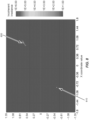
- FIG. 10A shows the intensity distribution of a ghost image from ray tracing simulation using the wavelength-selective filter 600 illustrated in FIG. 6 according to some embodiments.
- FIG. 10B shows the intensity distribution of a ghost image from ray tracing simulation using the wavelength-selective filter 900 illustrated in FIG. 9 that includes the "black coating” 910 according to some embodiments. As illustrated, the intensity of the ghost image may be significantly reduced by including the "black coating” 910 in the wavelength-selective filter 900.
- FIG. 10C shows the ratio of the ghost image intensity using the wavelength-selective filter 600 that does not include a "black coating” and the ghost image intensity using the wavelength-selective filter 900 with the "black coating” 910. As illustrated, the ghost image intensity can be reduced by as much as 20 fold by including the "black coating" 910 in the wavelength-selective filter 900.
- FIG. 11 illustrates a schematic cross-sectional diagram of a wavelength-selective filter 1100 according to some other embodiments.
- the filter 1100 may include a transparent substrate 1102, a first multilayer thin film 1110 formed on a front surface of the substrate 1102.
- the first multilayer thin film 1110 may be configured to have a first transmission band 430 in the NIR wavelength range and a second transmission band 440 in the visible wavelength range, as illustrated in FIG. 4A .
- the filter 1100 may further include a second multilayer thin film 1120 formed on the outer region of the first multilayer thin film 1110.
- the second multilayer thin film 1120 may be configured to be a high-pass filter similar to the wavelength-selective filter 500 illustrated in FIG. 5 .
- the filter 1100 may further include an anti-reflective coating 1130 formed on a back surface of the substrate 1102.
- the anti-reflective coating 1130 can prevent or reduce the amount of incoming light being reflected off of the back surface of the substrate 1102.
- the filter 1100 may further include a "black coating” 1140 formed on the back surface of the anti-reflective coating 1130.
- the "black coating” 1140 may be configured to absorb visible light and transmit NIR light as discussed above.
- FIG. 12 shows a transmittance curve 1210 and a reflectance curve 1220 of the "black coating” 1140 as a function of wavelength according to some embodiments.
- a transmittance curve 1230 of the first multilayer thin film 1110 is also shown.
- the "black coating" 1140 can be configured to have low transmittance values for the visible wavelength range from about 400 nm to about 700 nm, and high transmittance values in the NIR wavelength range from about 800 nm to about 950 nm.
- the "black coating” 1140 may have relatively high reflectance values in the wavelength range from about 700 nm to about 800 nm, but this may not significantly affect the performance of the wavelength-selective filter 1100 as light in this wavelength range is mostly blocked by the first multilayer thin film 1110 as evidenced by the transmittance curve 1230 of the first multilayer thin film 1110.
- the "black coating” 1140 has both low reflectance values and low transmittance values in the visible wavelength range.
- the "black coating” 1140 may substantially absorb visible light, thereby preventing visible light reflected off of the image sensor 620 (as illustrated in FIG. 9 ) from being transmitted and incident on the back side of the second multilayer thin film 606 to form a ghost image 624 on the image sensor 620.
- the anti-reflective coating 1130 is normally configured to have low reflectance values but high transmittance values. Thus, visible light reflected off of the image sensor 620 may be transmitted by the anti-reflective coating 1130 and be reflected by the second multilayer thin film 1120 to form the ghost image 624 on the image sensor 620 in absence of the "black coating" 1140.
- FIG. 13 shows a reflectance curve 1310 of the second multilayer thin film 1120 as a function of wavelength according to some embodiments.
- the second multilayer thin film 1120 may be configured to have low reflectance values (thus high transmittance values) only in the NIR wavelength range from about 800 nm to about 950 nm, and relatively high reflectance values for all other wavelengths.
- FIG. 13 also shows the reflectance curve 1220 of the "black coating" 1140, as well as the transmittance curve 1230 of the first multilayer thin film 1110. As illustrated, the low reflectance values of the "black coating" 1140 in the visible wavelength range may reduce reflection of light in the visible wavelength range, thereby reduce the intensity of the ghost image.
- FIG. 14 shows an exemplary quantum efficiency (Q.E.) curve 1410 as a function of wavelength of an image sensor 220 that may be used in the imaging system 200 as illustrated in FIG. 2 , according to an embodiment of the present invention.
- Q.E. quantum efficiency
- the quantum efficiency of the image sensor 220 in the visible (VIS) wavelength range can be as much as four times of the quantum efficiency in the NIR wavelength range. Therefore, a low f /# lens may allow too much visible light to pass through the imaging lens 210 to the image sensor 220 and may saturate the image sensor 220.
- the image sensor 220 in the imaging system 200 illustrated in FIG. 2 may comprise a charge-coupled device (CCD) or a complementary metal-oxide semiconductor (CMOS) device that converts light into electrons in a two-dimensional array of pixel cells.
- FIG. 15 illustrates schematically a plan view of the image sensor 220 according to an embodiment of the present invention.
- the image sensor 220 may include a two-dimensional array of pixel cells 222. The value of the accumulated charge of each pixel cell 222 may be read out to obtain an intensity distribution of the image.
- the imaging system 200 is used for computer vision in the visible wavelength range, it may be desirable to have the highest possible spatial resolution at the image sensor 220.
- the imaging system 200 is used for TOF depth sensing in the NIR wavelength range, it may be advantageous to have more light integration at the expense of pixel resolution to achieve better signal to noise ratio (SNR).
- SNR signal to noise ratio
- the image sensor 220 may be operated at different resolution modes for the visible wavelength range and the NIR wavelength range.
- the image sensor 220 may be operated at the native resolution for the visible wavelength range, i.e., at the maximum possible resolution that the physical pixel size of the image sensor can support.
- the image sensor 220 may be operated such that the accumulated charge in each pixel cell 222 is read out.
- the image sensor 220 may be operated at a resolution that is lower than the native resolution for greater light integration.
- FIG. 16 illustrates schematically a mode of operating the image sensor 220 according to an embodiment of the present invention.
- the two-dimensional array of pixel cells 222 may be binned into 2 ⁇ 2 groups 224.
- Each group 224 includes four pixel cells 222a-222d.
- This mode of operation can be referred to as image sensor pixel binning. In other embodiments, other binning configurations may be used.
- the pixel cells 222 of the image sensor 220 may be binned into n ⁇ n groups, where n is an integer greater than one.
- the pixels of the image sensor may also be binned into m ⁇ n groups, where m and n are integers and at least one of m and n is greater than one, and m may or may not be equal to n.
- the spatial resolution may be reduced as compared to the native resolution.
- the image sensor 220 is used in an imaging system that includes the wavelength-selective filter 214, 500, 600, 900, or 1100, since the spatial resolution of the imaging system (e.g., as measured by modulation transfer function or MTF) may be lower in the NIR wavelength range because of the greater effective aperture size, the reduction of spatial resolution at the image sensor may not be detrimental.
- MTF modulation transfer function
- binning may be performed at the analog level, where the value of the total accumulated charge for the m ⁇ n pixels in each group is read out. In such cases, the readout noise is not added.
- binning may be performed at the digital level, where the value of the accumulated charge for each pixel is read out, and the readout values for the m ⁇ n pixels in each group are then summed. In such cases, the readout noise is added in the summation process. Thus, the later embodiment may be more appropriate where the readout noise is relatively low.
- the imaging system 200 illustrated in FIG. 2 includes an imaging lens 210 that may be characterized by a lower f-number for NIR light and a higher f-number for visible light by utilizing a wavelength-selective filter 214 at its aperture stop, and an image sensor 220 that may be operated at a lower resolution mode for NIR light using pixel binning and at a higher resolution mode for visible light.
- the imaging system 200 may be suitable for use as a TOF depth sensor with active illumination in the NIR wavelength range where a faster lens and more light integration are desired, as well as a computer vision sensor with passive illumination in the visible wavelength range where higher image resolution and greater depth of field are desired.
- FIG. 17 is a schematic diagram illustrating an imaging system 1700 according to another embodiment of the present invention.
- the imaging system 1700 may include a plurality of lens elements 1702a-1702f, and a filter 214 positioned at the aperture stop 212.
- the imaging system 800 may further include a dichroic beam splitter 1710 positioned in the optical path after the filter 214.
- the dichroic beam splitter 1710 may be configured to transmit visible light along a first optical path, and reflect IR light along a second optical path.
- the imaging system 1700 may further include a first image sensor 1720 (VIS sensor) for visible light, and a second image sensor 1730 (IR sensor) for IR light.
- VIS sensor first image sensor 1720
- IR sensor IR sensor
- the first image sensor 1720 is disposed along the first optical path and configured to receive the visible light transmitted by the dichroic beam splitter 1710.
- the second image sensor 1730 is disposed along the second optical path and configured to receive the IR light reflected by the dichroic beam splitter 1710. In this fashion, visible light and IR light may be imaged by the first image sensor 1720 and the second image sensor 17830, respectively, at the same time.
- the first optical path to the first image sensor 1720 and the second optical path to the second image sensor 1730 are perpendicular to each other.
- FIG. 18 is a schematic diagram illustrating an imaging system 1800 according to yet another embodiment of the present invention.
- the imaging system 1800 is similar to the imaging system 1700 in that it also includes a dichroic beam splitter 1710 positioned after the filter 214, and configured to transmit visible light along a first optical path and to reflect IR light along a second optical path.
- the imaging system 1800 further includes a mirror 1810 positioned along the second optical path and configured to reflect IR light toward the second image sensor 1730. In this configuration, the first optical path to the first image sensor 1720 and the second optical path to the second image sensor 1730 are parallel to each other.
- the imaging system 1800 may further include a lens element 1820 positioned after the mirror 1810 along the second optical path for refocusing IR light at the second image sensor 1730.
- FIG. 19 is a simplified flowchart illustrating a method 1900 of operating an imaging system according to an embodiment of the present invention.
- the method 1900 includes performing three-dimensional sensing using the imaging system. In some embodiments, performing the three-dimensional sensing is performed in a first time slot.
- the imaging system may include a near infrared (NIR) light source, an imaging lens, and an image sensor positioned at an image plane of the imaging lens.
- NIR near infrared
- three-dimensional sensing may be performed by: emitting, using the NIR light source, a plurality of NIR light pulses toward one or more first objects (1910). A portion of each of the plurality of NIR light pulses may be reflected off of the one or more first objects.
- the method also includes receiving and focusing, using the imaging lens, the portion of each of the plurality of NIR light pulses reflected off of the one or more first objects onto the image sensor (1912).
- the imaging lens may include an aperture stop and a wavelength-selective filter positioned at the aperture stop.
- the wavelength-selective filter may have a first region and a second region surrounding the first region.
- the wavelength-selective filter is configured to transmit NIR light through both the first region and the second region, and to transmit visible light through the first region only.
- the method further includes detecting, using the image sensor, a three-dimensional image of the one or more first objects by determining a time of flight for the portion of each of the plurality of NIR light pulses from emission to detection (1914).
- the method 1900 further includes performing computer vision in a second time slot using the imaging system.
- Performing computer vision may be performed in a second time slot following the first time slot.
- computer vision may be performed by receiving and focusing, using the imaging lens, visible light from an ambient light source reflected off of one or more second objects onto the image sensor (1916), and detecting, using the image sensor, a two-dimensional intensity image of the one or more second objects (1918).
- some of the second objects can be the same as some of the first objects that were imaged in steps 1910-1914 described above.
- the image sensor includes a two dimensional array of pixels.
- detecting the three-dimensional image of the one or more first objects is performed by reading out a total amount of charge for each group of m ⁇ n pixels, where m and n are integers, and at least one of m and n is greater than one.
- detecting the three-dimensional image of the one or more first objects is performed by reading out an amount of charge for each pixel of the two-dimensional array of pixels, and calculating a total amount of charge for each group of m ⁇ n pixels by summing the amount of charge of the m ⁇ n pixels in each group, where m and n are integers, and at least one of m and n is greater than one.
- detecting the two-dimensional intensity image of the one or more second objects is performed by reading out an amount of charge for each pixel of the two-dimensional array of pixels.
- the method 1900 may include alternately performing three-dimensional sensing and computer vision in sequential time slots, and the duration of each time slot may range from about 1 ms to about 50 ms.
- the method 1900 may include performing three-dimensional sensing and computer vision simultaneously using an imaging system such as that illustrated in FIG. 17 or FIG. 18 .
- FIG. 19 provides a particular method of 1900 according to an embodiment of the present invention. Other sequences of steps may also be performed according to alternative embodiments. For example, alternative embodiments of the present invention may perform the steps outlined above in a different order. Moreover, the individual steps illustrated in FIG. 19 may include multiple sub-steps that may be performed in various sequences as appropriate to the individual step. Furthermore, additional steps may be added or removed depending on the particular applications.
- One of ordinary skill in the art would recognize many variations, modifications, and alternatives.
Landscapes
- Physics & Mathematics (AREA)
- Engineering & Computer Science (AREA)
- General Physics & Mathematics (AREA)
- Multimedia (AREA)
- Signal Processing (AREA)
- Optics & Photonics (AREA)
- Electromagnetism (AREA)
- Computer Networks & Wireless Communication (AREA)
- Radar, Positioning & Navigation (AREA)
- Remote Sensing (AREA)
- Health & Medical Sciences (AREA)
- Toxicology (AREA)
- Computer Vision & Pattern Recognition (AREA)
- Theoretical Computer Science (AREA)
- Studio Devices (AREA)
- Blocking Light For Cameras (AREA)
- Transforming Light Signals Into Electric Signals (AREA)
- Lenses (AREA)
- Optical Filters (AREA)
- Automatic Focus Adjustment (AREA)
- Optical Radar Systems And Details Thereof (AREA)
- Photometry And Measurement Of Optical Pulse Characteristics (AREA)
- Length Measuring Devices By Optical Means (AREA)
Priority Applications (1)
| Application Number | Priority Date | Filing Date | Title |
|---|---|---|---|
| EP24201057.7A EP4462799A3 (en) | 2016-11-10 | 2017-11-03 | Method and system for multiple f-number lens |
Applications Claiming Priority (2)
| Application Number | Priority Date | Filing Date | Title |
|---|---|---|---|
| US201662420249P | 2016-11-10 | 2016-11-10 | |
| PCT/US2017/059951 WO2018089266A1 (en) | 2016-11-10 | 2017-11-03 | Method and system for multiple f-number lens |
Related Child Applications (1)
| Application Number | Title | Priority Date | Filing Date |
|---|---|---|---|
| EP24201057.7A Division EP4462799A3 (en) | 2016-11-10 | 2017-11-03 | Method and system for multiple f-number lens |
Publications (3)
| Publication Number | Publication Date |
|---|---|
| EP3538840A1 EP3538840A1 (en) | 2019-09-18 |
| EP3538840A4 EP3538840A4 (en) | 2019-12-04 |
| EP3538840B1 true EP3538840B1 (en) | 2024-09-25 |
Family
ID=62064946
Family Applications (2)
| Application Number | Title | Priority Date | Filing Date |
|---|---|---|---|
| EP17869247.1A Active EP3538840B1 (en) | 2016-11-10 | 2017-11-03 | Method and system for multiple f-number lens |
| EP24201057.7A Pending EP4462799A3 (en) | 2016-11-10 | 2017-11-03 | Method and system for multiple f-number lens |
Family Applications After (1)
| Application Number | Title | Priority Date | Filing Date |
|---|---|---|---|
| EP24201057.7A Pending EP4462799A3 (en) | 2016-11-10 | 2017-11-03 | Method and system for multiple f-number lens |
Country Status (10)
| Country | Link |
|---|---|
| US (2) | US10659701B2 (enExample) |
| EP (2) | EP3538840B1 (enExample) |
| JP (2) | JP7093773B2 (enExample) |
| KR (2) | KR102507365B1 (enExample) |
| CN (2) | CN114143435B (enExample) |
| AU (1) | AU2017356847B2 (enExample) |
| CA (1) | CA3041852C (enExample) |
| IL (2) | IL266393B2 (enExample) |
| NZ (1) | NZ752710A (enExample) |
| WO (1) | WO2018089266A1 (enExample) |
Families Citing this family (19)
| Publication number | Priority date | Publication date | Assignee | Title |
|---|---|---|---|---|
| IL266393B2 (en) | 2016-11-10 | 2024-04-01 | Magic Leap Inc | Method and system for multiple F number lenses |
| US11080874B1 (en) * | 2018-01-05 | 2021-08-03 | Facebook Technologies, Llc | Apparatuses, systems, and methods for high-sensitivity active illumination imaging |
| WO2020154524A1 (en) | 2019-01-25 | 2020-07-30 | Magic Leap, Inc. | Eye-tracking using images having different exposure times |
| TWI691742B (zh) | 2019-02-01 | 2020-04-21 | 光芒光學股份有限公司 | 鏡頭 |
| WO2020236827A1 (en) | 2019-05-20 | 2020-11-26 | Magic Leap, Inc. | Systems and techniques for estimating eye pose |
| TWI745745B (zh) | 2019-09-10 | 2021-11-11 | 光芒光學股份有限公司 | 取像鏡頭與遮光元件的製作方法 |
| FR3105453B1 (fr) * | 2019-12-23 | 2023-08-25 | Latelec | Module optique pour l’éclairage et la transmission de données par la technologie Li-Fi |
| WO2021235778A1 (ko) | 2020-05-22 | 2021-11-25 | 주식회사 에스오에스랩 | 라이다 장치 |
| KR102817675B1 (ko) | 2020-07-15 | 2025-06-09 | 매직 립, 인코포레이티드 | 비구면 각막 모델을 사용한 눈 추적 |
| US11853845B2 (en) * | 2020-09-02 | 2023-12-26 | Cognex Corporation | Machine vision system and method with multi-aperture optics assembly |
| CA3201941A1 (en) * | 2020-11-15 | 2022-05-19 | Qioptiq Limited | Retroreflection defeat filter |
| CN113031367A (zh) * | 2021-03-12 | 2021-06-25 | 杭州海康威视数字技术股份有限公司 | 一种多光谱镜头和多光谱摄像机 |
| CN115453706A (zh) * | 2021-06-09 | 2022-12-09 | 浙江舜宇光学有限公司 | 摄像镜头 |
| CN115097604B (zh) * | 2022-07-05 | 2023-10-24 | 杭州海康威视数字技术股份有限公司 | 一种多光谱镜头和一种多光谱摄像装置 |
| WO2024013142A1 (en) * | 2022-07-15 | 2024-01-18 | Lightcode Photonics Oü | Image capture device with wavelength separation device |
| CN115047433B (zh) * | 2022-08-16 | 2022-11-01 | 杭州宇称电子技术有限公司 | 用于tof距离量测系统光学自动化调整方法及其应用 |
| CN117717306A (zh) * | 2024-01-30 | 2024-03-19 | 敏捷医疗科技(苏州)有限公司 | 内窥镜成像模组及具有其的内窥镜、手术器械 |
| WO2025201872A1 (en) * | 2024-03-25 | 2025-10-02 | Sony Semiconductor Solutions Corporation | A sensing module for combined imaging and depth sensing, an optical system, a method and computer program |
| CN119717205B (zh) * | 2024-12-26 | 2025-11-18 | 中国核工业第五建设有限公司 | 用于采集焊接图像的光学成像镜头及光学成像装置 |
Family Cites Families (36)
| Publication number | Priority date | Publication date | Assignee | Title |
|---|---|---|---|---|
| US6593574B2 (en) * | 1999-09-16 | 2003-07-15 | Wayne State University | Hand-held sound source gun for infrared imaging of sub-surface defects in materials |
| US6578987B1 (en) * | 2000-05-03 | 2003-06-17 | Vari-Lite, Inc. | Intra-lens color and dimming apparatus |
| JP3905696B2 (ja) * | 2000-11-07 | 2007-04-18 | ペンタックス株式会社 | 3次元画像入力装置 |
| JP3726699B2 (ja) * | 2001-04-20 | 2005-12-14 | 日本ビクター株式会社 | 光学撮像装置、光学測距装置 |
| JP4010779B2 (ja) * | 2001-06-08 | 2007-11-21 | ペンタックス株式会社 | 画像検出装置と絞り装置 |
| JP2005004181A (ja) * | 2003-05-21 | 2005-01-06 | Fujinon Corp | 可視光・赤外光撮影用レンズシステム |
| US7297951B2 (en) * | 2005-07-27 | 2007-11-20 | Raytheon Company | Two F-number, two-color sensor system |
| US7400458B2 (en) * | 2005-08-12 | 2008-07-15 | Philips Lumileds Lighting Company, Llc | Imaging optics with wavelength dependent aperture stop |
| JP4508279B2 (ja) * | 2008-07-17 | 2010-07-21 | ソニー株式会社 | 画像処理装置、画像処理方法、及び、プログラム |
| DE102008048379B4 (de) * | 2008-09-22 | 2016-03-31 | Schott Ag | Verfahren zur Herstellung eines Linsen-Arrays |
| US8988508B2 (en) * | 2010-09-24 | 2015-03-24 | Microsoft Technology Licensing, Llc. | Wide angle field of view active illumination imaging system |
| KR101925137B1 (ko) * | 2010-10-29 | 2018-12-06 | 삼성전자주식회사 | 전기 신호를 이용하여 선택적으로 가시광선과 적외선을 투과하는 필터 |
| US8749796B2 (en) | 2011-08-09 | 2014-06-10 | Primesense Ltd. | Projectors of structured light |
| US9063574B1 (en) * | 2012-03-14 | 2015-06-23 | Amazon Technologies, Inc. | Motion detection systems for electronic devices |
| US9036080B2 (en) * | 2012-09-04 | 2015-05-19 | Canon Kabushiki Kaisha | Apparatus and method for acquiring information about light-field data |
| KR101933994B1 (ko) * | 2012-10-16 | 2018-12-31 | 삼성전자주식회사 | 깊이 영상과 컬러 영상을 획득하는 픽셀 구조를 가진 이미지 센서 |
| KR20140055025A (ko) * | 2012-10-30 | 2014-05-09 | 삼성전자주식회사 | 깊이 영상을 센싱하는 영상 센싱 장치 |
| EP2946339A4 (en) * | 2013-01-17 | 2016-09-14 | Sionyx Llc | BIOMETRIC IMAGING DEVICES AND CORRESPONDING METHODS |
| US9134114B2 (en) * | 2013-03-11 | 2015-09-15 | Texas Instruments Incorporated | Time of flight sensor binning |
| KR102112298B1 (ko) | 2013-09-30 | 2020-05-18 | 삼성전자주식회사 | 컬러 영상 및 깊이 영상을 생성하는 방법 및 장치 |
| DE102014103010A1 (de) * | 2014-03-06 | 2015-09-10 | Skidata Ag | Digitalkamera |
| US20170026588A1 (en) * | 2014-05-01 | 2017-01-26 | Rebellion Photonics, Inc. | Dual-band divided-aperture infra-red spectral imaging system |
| US9825074B2 (en) * | 2014-06-10 | 2017-11-21 | Invisage Technologies, Inc. | Layout and operation of pixels for image sensors |
| US9805454B2 (en) * | 2014-07-15 | 2017-10-31 | Microsoft Technology Licensing, Llc | Wide field-of-view depth imaging |
| US10152631B2 (en) * | 2014-08-08 | 2018-12-11 | Fotonation Limited | Optical system for an image acquisition device |
| KR101834393B1 (ko) * | 2014-08-08 | 2018-04-13 | 포토내이션 리미티드 | 이미지 획득 장치용 광학계 |
| WO2016118473A1 (en) | 2015-01-20 | 2016-07-28 | Eyelock Llc | Lens system for high quality visible image acquisition and infra-red iris image acquisition |
| US20160262602A1 (en) * | 2015-03-09 | 2016-09-15 | Steven Sounyoung Yu | Laparoscopic Cholecystectomy With Fluorescence Cholangiography |
| WO2016168378A1 (en) * | 2015-04-13 | 2016-10-20 | Gerard Dirk Smits | Machine vision for ego-motion, segmenting, and classifying objects |
| KR101748260B1 (ko) * | 2015-04-23 | 2017-06-16 | 엘지전자 주식회사 | 카메라 모듈 |
| JP6442065B2 (ja) * | 2015-09-16 | 2018-12-19 | 富士フイルム株式会社 | フォーカス装置,撮像システムおよびフォーカス駆動信号出力方法 |
| CN108024696B (zh) * | 2015-09-18 | 2020-01-07 | 奥林巴斯株式会社 | 内窥镜装置 |
| US20170155873A1 (en) * | 2015-11-30 | 2017-06-01 | Sensors Unlimited, Inc. | Sensor systems and methods |
| US10475171B2 (en) * | 2016-01-22 | 2019-11-12 | Hera Systems, Inc. | Multi-camera imaging system for nanosatellites |
| CN105911559A (zh) * | 2016-06-02 | 2016-08-31 | 中国科学院光电研究院 | 基于可见光-近红外-短波红外波段的激光雷达系统 |
| IL266393B2 (en) | 2016-11-10 | 2024-04-01 | Magic Leap Inc | Method and system for multiple F number lenses |
-
2017
- 2017-11-03 IL IL266393A patent/IL266393B2/en unknown
- 2017-11-03 EP EP17869247.1A patent/EP3538840B1/en active Active
- 2017-11-03 CA CA3041852A patent/CA3041852C/en active Active
- 2017-11-03 AU AU2017356847A patent/AU2017356847B2/en active Active
- 2017-11-03 KR KR1020227008654A patent/KR102507365B1/ko active Active
- 2017-11-03 CN CN202111508715.4A patent/CN114143435B/zh active Active
- 2017-11-03 JP JP2019524158A patent/JP7093773B2/ja active Active
- 2017-11-03 KR KR1020197014775A patent/KR102377023B1/ko active Active
- 2017-11-03 US US15/803,351 patent/US10659701B2/en active Active
- 2017-11-03 CN CN201780069250.2A patent/CN109964097B/zh active Active
- 2017-11-03 NZ NZ752710A patent/NZ752710A/en unknown
- 2017-11-03 IL IL308136A patent/IL308136A/en unknown
- 2017-11-03 WO PCT/US2017/059951 patent/WO2018089266A1/en not_active Ceased
- 2017-11-03 EP EP24201057.7A patent/EP4462799A3/en active Pending
-
2020
- 2020-04-10 US US16/846,027 patent/US11240422B2/en active Active
-
2022
- 2022-03-11 JP JP2022038046A patent/JP7420849B2/ja active Active
Also Published As
| Publication number | Publication date |
|---|---|
| CN114143435A (zh) | 2022-03-04 |
| KR102507365B1 (ko) | 2023-03-07 |
| EP4462799A3 (en) | 2025-04-02 |
| CA3041852A1 (en) | 2018-05-17 |
| KR102377023B1 (ko) | 2022-03-21 |
| US20200244857A1 (en) | 2020-07-30 |
| EP3538840A1 (en) | 2019-09-18 |
| CN109964097B (zh) | 2021-12-14 |
| JP7420849B2 (ja) | 2024-01-23 |
| US10659701B2 (en) | 2020-05-19 |
| NZ752710A (en) | 2023-09-29 |
| JP2022066564A (ja) | 2022-04-28 |
| IL266393B2 (en) | 2024-04-01 |
| CA3041852C (en) | 2023-07-18 |
| WO2018089266A1 (en) | 2018-05-17 |
| CN114143435B (zh) | 2024-09-03 |
| IL266393B1 (en) | 2023-12-01 |
| IL266393A (en) | 2019-06-30 |
| EP4462799A2 (en) | 2024-11-13 |
| AU2017356847B2 (en) | 2022-11-17 |
| US20180131853A1 (en) | 2018-05-10 |
| CN109964097A (zh) | 2019-07-02 |
| KR20190084993A (ko) | 2019-07-17 |
| JP2019537895A (ja) | 2019-12-26 |
| JP7093773B2 (ja) | 2022-06-30 |
| US11240422B2 (en) | 2022-02-01 |
| AU2017356847A1 (en) | 2019-05-02 |
| KR20220038828A (ko) | 2022-03-29 |
| IL308136A (en) | 2023-12-01 |
| EP3538840A4 (en) | 2019-12-04 |
Similar Documents
| Publication | Publication Date | Title |
|---|---|---|
| US11240422B2 (en) | Method and system for multiple f-number lens | |
| EP3338305B1 (en) | System and method to extend near infrared spectral response for imaging systems | |
| JP5737971B2 (ja) | 固体撮像装置およびカメラ | |
| JP2019537895A5 (enExample) | ||
| CN106033761B (zh) | 具有非平面光学界面的背面照度图像传感器 | |
| US20220210316A1 (en) | Image pickup apparatus of measuring distance from subject to image pickup surface of image pickup device and method for controlling the same | |
| JP4532968B2 (ja) | 焦点検出装置 | |
| NZ794045A (en) | Method and system for multiple f-number lens | |
| FR2783930A1 (fr) | Appareil de mesure de distance | |
| JP6127973B2 (ja) | 撮像装置及び撮像装置用の撮像素子 | |
| CN112558038A (zh) | 一种激光雷达的扫描方法 | |
| CN114777922B (zh) | 成像光谱仪光学系统 | |
| CN114690339A (zh) | 具有用于减少串扰的滤光器和挡板的Lidar接收器 | |
| RU2543688C2 (ru) | Камера и оптическая система для получения 3d изображений (варианты) | |
| CN117528063A (zh) | 一种手机摄像头景深测量的光学装置及方法 | |
| CN117528239A (zh) | 摄像模组、对焦方法、装置、电子设备及介质 | |
| JPS61233713A (ja) | 2方式の焦点検出手段を有した光学系 |
Legal Events
| Date | Code | Title | Description |
|---|---|---|---|
| STAA | Information on the status of an ep patent application or granted ep patent |
Free format text: STATUS: THE INTERNATIONAL PUBLICATION HAS BEEN MADE |
|
| PUAI | Public reference made under article 153(3) epc to a published international application that has entered the european phase |
Free format text: ORIGINAL CODE: 0009012 |
|
| STAA | Information on the status of an ep patent application or granted ep patent |
Free format text: STATUS: REQUEST FOR EXAMINATION WAS MADE |
|
| 17P | Request for examination filed |
Effective date: 20190528 |
|
| AK | Designated contracting states |
Kind code of ref document: A1 Designated state(s): AL AT BE BG CH CY CZ DE DK EE ES FI FR GB GR HR HU IE IS IT LI LT LU LV MC MK MT NL NO PL PT RO RS SE SI SK SM TR |
|
| AX | Request for extension of the european patent |
Extension state: BA ME |
|
| A4 | Supplementary search report drawn up and despatched |
Effective date: 20191031 |
|
| RIC1 | Information provided on ipc code assigned before grant |
Ipc: G01B 11/22 20060101AFI20191025BHEP Ipc: H04N 5/3745 20110101ALI20191025BHEP Ipc: H01L 27/14 20060101ALI20191025BHEP Ipc: H04N 5/33 20060101ALI20191025BHEP |
|
| DAV | Request for validation of the european patent (deleted) | ||
| DAX | Request for extension of the european patent (deleted) | ||
| REG | Reference to a national code |
Ref country code: HK Ref legal event code: DE Ref document number: 40014550 Country of ref document: HK |
|
| STAA | Information on the status of an ep patent application or granted ep patent |
Free format text: STATUS: EXAMINATION IS IN PROGRESS |
|
| 17Q | First examination report despatched |
Effective date: 20220609 |
|
| P01 | Opt-out of the competence of the unified patent court (upc) registered |
Effective date: 20230607 |
|
| REG | Reference to a national code |
Ref country code: DE Ref legal event code: R079 Free format text: PREVIOUS MAIN CLASS: G01B0011220000 Ipc: H04N0005330000 Ref country code: DE Ref legal event code: R079 Ref document number: 602017085130 Country of ref document: DE Free format text: PREVIOUS MAIN CLASS: G01B0011220000 Ipc: H04N0005330000 |
|
| GRAP | Despatch of communication of intention to grant a patent |
Free format text: ORIGINAL CODE: EPIDOSNIGR1 |
|
| STAA | Information on the status of an ep patent application or granted ep patent |
Free format text: STATUS: GRANT OF PATENT IS INTENDED |
|
| RIC1 | Information provided on ipc code assigned before grant |
Ipc: H04N 23/667 20230101ALI20240314BHEP Ipc: H04N 23/56 20230101ALI20240314BHEP Ipc: H04N 23/55 20230101ALI20240314BHEP Ipc: G01S 17/894 20200101ALI20240314BHEP Ipc: H04N 13/254 20180101ALI20240314BHEP Ipc: G02B 27/14 20060101ALI20240314BHEP Ipc: G02B 27/10 20060101ALI20240314BHEP Ipc: G02B 27/00 20060101ALI20240314BHEP Ipc: G02B 13/14 20060101ALI20240314BHEP Ipc: G02B 5/20 20060101ALI20240314BHEP Ipc: G01S 7/481 20060101ALI20240314BHEP Ipc: H04N 5/33 20060101AFI20240314BHEP |
|
| INTG | Intention to grant announced |
Effective date: 20240416 |
|
| GRAS | Grant fee paid |
Free format text: ORIGINAL CODE: EPIDOSNIGR3 |
|
| GRAA | (expected) grant |
Free format text: ORIGINAL CODE: 0009210 |
|
| STAA | Information on the status of an ep patent application or granted ep patent |
Free format text: STATUS: THE PATENT HAS BEEN GRANTED |
|
| AK | Designated contracting states |
Kind code of ref document: B1 Designated state(s): AL AT BE BG CH CY CZ DE DK EE ES FI FR GB GR HR HU IE IS IT LI LT LU LV MC MK MT NL NO PL PT RO RS SE SI SK SM TR |
|
| REG | Reference to a national code |
Ref country code: GB Ref legal event code: FG4D |
|
| REG | Reference to a national code |
Ref country code: CH Ref legal event code: EP |
|
| REG | Reference to a national code |
Ref country code: DE Ref legal event code: R096 Ref document number: 602017085130 Country of ref document: DE |
|
| REG | Reference to a national code |
Ref country code: IE Ref legal event code: FG4D Ref country code: NL Ref legal event code: FP |
|
| REG | Reference to a national code |
Ref country code: LT Ref legal event code: MG9D |
|
| PG25 | Lapsed in a contracting state [announced via postgrant information from national office to epo] |
Ref country code: NO Free format text: LAPSE BECAUSE OF FAILURE TO SUBMIT A TRANSLATION OF THE DESCRIPTION OR TO PAY THE FEE WITHIN THE PRESCRIBED TIME-LIMIT Effective date: 20241225 |
|
| PG25 | Lapsed in a contracting state [announced via postgrant information from national office to epo] |
Ref country code: GR Free format text: LAPSE BECAUSE OF FAILURE TO SUBMIT A TRANSLATION OF THE DESCRIPTION OR TO PAY THE FEE WITHIN THE PRESCRIBED TIME-LIMIT Effective date: 20241226 Ref country code: FI Free format text: LAPSE BECAUSE OF FAILURE TO SUBMIT A TRANSLATION OF THE DESCRIPTION OR TO PAY THE FEE WITHIN THE PRESCRIBED TIME-LIMIT Effective date: 20240925 |
|
| PGFP | Annual fee paid to national office [announced via postgrant information from national office to epo] |
Ref country code: BE Payment date: 20241022 Year of fee payment: 8 |
|
| PGFP | Annual fee paid to national office [announced via postgrant information from national office to epo] |
Ref country code: GB Payment date: 20241022 Year of fee payment: 8 |
|
| PG25 | Lapsed in a contracting state [announced via postgrant information from national office to epo] |
Ref country code: BG Free format text: LAPSE BECAUSE OF FAILURE TO SUBMIT A TRANSLATION OF THE DESCRIPTION OR TO PAY THE FEE WITHIN THE PRESCRIBED TIME-LIMIT Effective date: 20240925 |
|
| PG25 | Lapsed in a contracting state [announced via postgrant information from national office to epo] |
Ref country code: LV Free format text: LAPSE BECAUSE OF FAILURE TO SUBMIT A TRANSLATION OF THE DESCRIPTION OR TO PAY THE FEE WITHIN THE PRESCRIBED TIME-LIMIT Effective date: 20240925 |
|
| PGFP | Annual fee paid to national office [announced via postgrant information from national office to epo] |
Ref country code: FR Payment date: 20241022 Year of fee payment: 8 |
|
| PG25 | Lapsed in a contracting state [announced via postgrant information from national office to epo] |
Ref country code: RS Free format text: LAPSE BECAUSE OF FAILURE TO SUBMIT A TRANSLATION OF THE DESCRIPTION OR TO PAY THE FEE WITHIN THE PRESCRIBED TIME-LIMIT Effective date: 20241225 |
|
| PG25 | Lapsed in a contracting state [announced via postgrant information from national office to epo] |
Ref country code: RS Free format text: LAPSE BECAUSE OF FAILURE TO SUBMIT A TRANSLATION OF THE DESCRIPTION OR TO PAY THE FEE WITHIN THE PRESCRIBED TIME-LIMIT Effective date: 20241225 Ref country code: NO Free format text: LAPSE BECAUSE OF FAILURE TO SUBMIT A TRANSLATION OF THE DESCRIPTION OR TO PAY THE FEE WITHIN THE PRESCRIBED TIME-LIMIT Effective date: 20241225 Ref country code: LV Free format text: LAPSE BECAUSE OF FAILURE TO SUBMIT A TRANSLATION OF THE DESCRIPTION OR TO PAY THE FEE WITHIN THE PRESCRIBED TIME-LIMIT Effective date: 20240925 Ref country code: GR Free format text: LAPSE BECAUSE OF FAILURE TO SUBMIT A TRANSLATION OF THE DESCRIPTION OR TO PAY THE FEE WITHIN THE PRESCRIBED TIME-LIMIT Effective date: 20241226 Ref country code: FI Free format text: LAPSE BECAUSE OF FAILURE TO SUBMIT A TRANSLATION OF THE DESCRIPTION OR TO PAY THE FEE WITHIN THE PRESCRIBED TIME-LIMIT Effective date: 20240925 Ref country code: BG Free format text: LAPSE BECAUSE OF FAILURE TO SUBMIT A TRANSLATION OF THE DESCRIPTION OR TO PAY THE FEE WITHIN THE PRESCRIBED TIME-LIMIT Effective date: 20240925 |
|
| REG | Reference to a national code |
Ref country code: AT Ref legal event code: MK05 Ref document number: 1727631 Country of ref document: AT Kind code of ref document: T Effective date: 20240925 |
|
| PG25 | Lapsed in a contracting state [announced via postgrant information from national office to epo] |
Ref country code: PT Free format text: LAPSE BECAUSE OF FAILURE TO SUBMIT A TRANSLATION OF THE DESCRIPTION OR TO PAY THE FEE WITHIN THE PRESCRIBED TIME-LIMIT Effective date: 20250127 Ref country code: IS Free format text: LAPSE BECAUSE OF FAILURE TO SUBMIT A TRANSLATION OF THE DESCRIPTION OR TO PAY THE FEE WITHIN THE PRESCRIBED TIME-LIMIT Effective date: 20250125 |
|
| PG25 | Lapsed in a contracting state [announced via postgrant information from national office to epo] |
Ref country code: RO Free format text: LAPSE BECAUSE OF FAILURE TO SUBMIT A TRANSLATION OF THE DESCRIPTION OR TO PAY THE FEE WITHIN THE PRESCRIBED TIME-LIMIT Effective date: 20240925 Ref country code: SM Free format text: LAPSE BECAUSE OF FAILURE TO SUBMIT A TRANSLATION OF THE DESCRIPTION OR TO PAY THE FEE WITHIN THE PRESCRIBED TIME-LIMIT Effective date: 20240925 |
|
| PG25 | Lapsed in a contracting state [announced via postgrant information from national office to epo] |
Ref country code: ES Free format text: LAPSE BECAUSE OF FAILURE TO SUBMIT A TRANSLATION OF THE DESCRIPTION OR TO PAY THE FEE WITHIN THE PRESCRIBED TIME-LIMIT Effective date: 20240925 |
|
| PG25 | Lapsed in a contracting state [announced via postgrant information from national office to epo] |
Ref country code: EE Free format text: LAPSE BECAUSE OF FAILURE TO SUBMIT A TRANSLATION OF THE DESCRIPTION OR TO PAY THE FEE WITHIN THE PRESCRIBED TIME-LIMIT Effective date: 20240925 Ref country code: AT Free format text: LAPSE BECAUSE OF FAILURE TO SUBMIT A TRANSLATION OF THE DESCRIPTION OR TO PAY THE FEE WITHIN THE PRESCRIBED TIME-LIMIT Effective date: 20240925 |
|
| PG25 | Lapsed in a contracting state [announced via postgrant information from national office to epo] |
Ref country code: PL Free format text: LAPSE BECAUSE OF FAILURE TO SUBMIT A TRANSLATION OF THE DESCRIPTION OR TO PAY THE FEE WITHIN THE PRESCRIBED TIME-LIMIT Effective date: 20240925 Ref country code: CZ Free format text: LAPSE BECAUSE OF FAILURE TO SUBMIT A TRANSLATION OF THE DESCRIPTION OR TO PAY THE FEE WITHIN THE PRESCRIBED TIME-LIMIT Effective date: 20240925 |
|
| PG25 | Lapsed in a contracting state [announced via postgrant information from national office to epo] |
Ref country code: IT Free format text: LAPSE BECAUSE OF FAILURE TO SUBMIT A TRANSLATION OF THE DESCRIPTION OR TO PAY THE FEE WITHIN THE PRESCRIBED TIME-LIMIT Effective date: 20240925 Ref country code: SK Free format text: LAPSE BECAUSE OF FAILURE TO SUBMIT A TRANSLATION OF THE DESCRIPTION OR TO PAY THE FEE WITHIN THE PRESCRIBED TIME-LIMIT Effective date: 20240925 |
|
| REG | Reference to a national code |
Ref country code: DE Ref legal event code: R097 Ref document number: 602017085130 Country of ref document: DE |
|
| REG | Reference to a national code |
Ref country code: CH Ref legal event code: PL |
|
| PG25 | Lapsed in a contracting state [announced via postgrant information from national office to epo] |
Ref country code: MC Free format text: LAPSE BECAUSE OF FAILURE TO SUBMIT A TRANSLATION OF THE DESCRIPTION OR TO PAY THE FEE WITHIN THE PRESCRIBED TIME-LIMIT Effective date: 20240925 |
|
| PG25 | Lapsed in a contracting state [announced via postgrant information from national office to epo] |
Ref country code: DK Free format text: LAPSE BECAUSE OF FAILURE TO SUBMIT A TRANSLATION OF THE DESCRIPTION OR TO PAY THE FEE WITHIN THE PRESCRIBED TIME-LIMIT Effective date: 20240925 |
|
| PG25 | Lapsed in a contracting state [announced via postgrant information from national office to epo] |
Ref country code: LU Free format text: LAPSE BECAUSE OF NON-PAYMENT OF DUE FEES Effective date: 20241103 |
|
| REG | Reference to a national code |
Ref country code: CH Ref legal event code: PL |
|
| PG25 | Lapsed in a contracting state [announced via postgrant information from national office to epo] |
Ref country code: CH Free format text: LAPSE BECAUSE OF NON-PAYMENT OF DUE FEES Effective date: 20241130 |
|
| PLBE | No opposition filed within time limit |
Free format text: ORIGINAL CODE: 0009261 |
|
| STAA | Information on the status of an ep patent application or granted ep patent |
Free format text: STATUS: NO OPPOSITION FILED WITHIN TIME LIMIT |
|
| 26N | No opposition filed |
Effective date: 20250626 |
|
| PG25 | Lapsed in a contracting state [announced via postgrant information from national office to epo] |
Ref country code: SE Free format text: LAPSE BECAUSE OF FAILURE TO SUBMIT A TRANSLATION OF THE DESCRIPTION OR TO PAY THE FEE WITHIN THE PRESCRIBED TIME-LIMIT Effective date: 20240925 |
|
| PG25 | Lapsed in a contracting state [announced via postgrant information from national office to epo] |
Ref country code: IE Free format text: LAPSE BECAUSE OF NON-PAYMENT OF DUE FEES Effective date: 20241103 |
|
| PGFP | Annual fee paid to national office [announced via postgrant information from national office to epo] |
Ref country code: NL Payment date: 20251022 Year of fee payment: 9 |
|
| PGFP | Annual fee paid to national office [announced via postgrant information from national office to epo] |
Ref country code: DE Payment date: 20251022 Year of fee payment: 9 |