EP3338305B1 - System and method to extend near infrared spectral response for imaging systems - Google Patents
System and method to extend near infrared spectral response for imaging systems Download PDFInfo
- Publication number
- EP3338305B1 EP3338305B1 EP16750551.0A EP16750551A EP3338305B1 EP 3338305 B1 EP3338305 B1 EP 3338305B1 EP 16750551 A EP16750551 A EP 16750551A EP 3338305 B1 EP3338305 B1 EP 3338305B1
- Authority
- EP
- European Patent Office
- Prior art keywords
- photodetector region
- light
- array
- sensor
- photodetector
- Prior art date
- Legal status (The legal status is an assumption and is not a legal conclusion. Google has not performed a legal analysis and makes no representation as to the accuracy of the status listed.)
- Active
Links
- 238000000034 method Methods 0.000 title claims description 62
- 230000004044 response Effects 0.000 title description 11
- 230000003595 spectral effect Effects 0.000 title description 11
- 238000003384 imaging method Methods 0.000 title description 8
- 239000000758 substrate Substances 0.000 claims description 32
- 230000000737 periodic effect Effects 0.000 claims description 12
- 238000004519 manufacturing process Methods 0.000 claims description 10
- 230000001902 propagating effect Effects 0.000 claims description 5
- 230000003667 anti-reflective effect Effects 0.000 claims description 4
- 229910052751 metal Inorganic materials 0.000 description 73
- 239000002184 metal Substances 0.000 description 73
- 230000015654 memory Effects 0.000 description 27
- 230000008569 process Effects 0.000 description 15
- 239000000463 material Substances 0.000 description 13
- 230000006870 function Effects 0.000 description 12
- 238000012546 transfer Methods 0.000 description 10
- 230000003936 working memory Effects 0.000 description 10
- 238000012545 processing Methods 0.000 description 9
- 238000010276 construction Methods 0.000 description 8
- 238000002955 isolation Methods 0.000 description 8
- 230000009471 action Effects 0.000 description 7
- XUIMIQQOPSSXEZ-UHFFFAOYSA-N Silicon Chemical compound [Si] XUIMIQQOPSSXEZ-UHFFFAOYSA-N 0.000 description 6
- 230000003287 optical effect Effects 0.000 description 6
- 229910052710 silicon Inorganic materials 0.000 description 6
- 239000010703 silicon Substances 0.000 description 6
- 238000004891 communication Methods 0.000 description 5
- 238000010586 diagram Methods 0.000 description 5
- 238000005516 engineering process Methods 0.000 description 5
- 238000004590 computer program Methods 0.000 description 4
- 230000035515 penetration Effects 0.000 description 4
- 238000006243 chemical reaction Methods 0.000 description 3
- 238000013461 design Methods 0.000 description 3
- 238000005286 illumination Methods 0.000 description 3
- 239000004065 semiconductor Substances 0.000 description 3
- VYPSYNLAJGMNEJ-UHFFFAOYSA-N Silicium dioxide Chemical compound O=[Si]=O VYPSYNLAJGMNEJ-UHFFFAOYSA-N 0.000 description 2
- 230000015572 biosynthetic process Effects 0.000 description 2
- 230000007423 decrease Effects 0.000 description 2
- 239000011521 glass Substances 0.000 description 2
- 230000004048 modification Effects 0.000 description 2
- 238000012986 modification Methods 0.000 description 2
- BASFCYQUMIYNBI-UHFFFAOYSA-N platinum Chemical compound [Pt] BASFCYQUMIYNBI-UHFFFAOYSA-N 0.000 description 2
- 230000001681 protective effect Effects 0.000 description 2
- 239000007787 solid Substances 0.000 description 2
- VYZAMTAEIAYCRO-UHFFFAOYSA-N Chromium Chemical compound [Cr] VYZAMTAEIAYCRO-UHFFFAOYSA-N 0.000 description 1
- RYGMFSIKBFXOCR-UHFFFAOYSA-N Copper Chemical compound [Cu] RYGMFSIKBFXOCR-UHFFFAOYSA-N 0.000 description 1
- 229910052581 Si3N4 Inorganic materials 0.000 description 1
- BQCADISMDOOEFD-UHFFFAOYSA-N Silver Chemical compound [Ag] BQCADISMDOOEFD-UHFFFAOYSA-N 0.000 description 1
- 238000010521 absorption reaction Methods 0.000 description 1
- 239000008186 active pharmaceutical agent Substances 0.000 description 1
- 229910052782 aluminium Inorganic materials 0.000 description 1
- XAGFODPZIPBFFR-UHFFFAOYSA-N aluminium Chemical compound [Al] XAGFODPZIPBFFR-UHFFFAOYSA-N 0.000 description 1
- 230000004888 barrier function Effects 0.000 description 1
- 230000006399 behavior Effects 0.000 description 1
- 230000009286 beneficial effect Effects 0.000 description 1
- 230000005540 biological transmission Effects 0.000 description 1
- 229910052804 chromium Inorganic materials 0.000 description 1
- 239000011651 chromium Substances 0.000 description 1
- 229910052802 copper Inorganic materials 0.000 description 1
- 239000010949 copper Substances 0.000 description 1
- 230000008878 coupling Effects 0.000 description 1
- 238000010168 coupling process Methods 0.000 description 1
- 238000005859 coupling reaction Methods 0.000 description 1
- 230000001419 dependent effect Effects 0.000 description 1
- 229910003460 diamond Inorganic materials 0.000 description 1
- 239000010432 diamond Substances 0.000 description 1
- 239000003989 dielectric material Substances 0.000 description 1
- 230000005611 electricity Effects 0.000 description 1
- PCHJSUWPFVWCPO-UHFFFAOYSA-N gold Chemical compound [Au] PCHJSUWPFVWCPO-UHFFFAOYSA-N 0.000 description 1
- 229910052737 gold Inorganic materials 0.000 description 1
- 239000010931 gold Substances 0.000 description 1
- CJNBYAVZURUTKZ-UHFFFAOYSA-N hafnium(IV) oxide Inorganic materials O=[Hf]=O CJNBYAVZURUTKZ-UHFFFAOYSA-N 0.000 description 1
- 239000007943 implant Substances 0.000 description 1
- 238000013507 mapping Methods 0.000 description 1
- 238000005259 measurement Methods 0.000 description 1
- 238000002844 melting Methods 0.000 description 1
- 230000008018 melting Effects 0.000 description 1
- 238000012634 optical imaging Methods 0.000 description 1
- 239000005022 packaging material Substances 0.000 description 1
- 230000000149 penetrating effect Effects 0.000 description 1
- 229910052697 platinum Inorganic materials 0.000 description 1
- 230000009467 reduction Effects 0.000 description 1
- 229910052703 rhodium Inorganic materials 0.000 description 1
- 239000010948 rhodium Substances 0.000 description 1
- MHOVAHRLVXNVSD-UHFFFAOYSA-N rhodium atom Chemical compound [Rh] MHOVAHRLVXNVSD-UHFFFAOYSA-N 0.000 description 1
- 239000000377 silicon dioxide Substances 0.000 description 1
- 235000012239 silicon dioxide Nutrition 0.000 description 1
- 239000002210 silicon-based material Substances 0.000 description 1
- 229910052709 silver Inorganic materials 0.000 description 1
- 239000004332 silver Substances 0.000 description 1
- 230000003068 static effect Effects 0.000 description 1
- 239000003826 tablet Substances 0.000 description 1
- PBCFLUZVCVVTBY-UHFFFAOYSA-N tantalum pentoxide Inorganic materials O=[Ta](=O)O[Ta](=O)=O PBCFLUZVCVVTBY-UHFFFAOYSA-N 0.000 description 1
Images


Classifications
-
- H—ELECTRICITY
- H01—ELECTRIC ELEMENTS
- H01L—SEMICONDUCTOR DEVICES NOT COVERED BY CLASS H10
- H01L27/00—Devices consisting of a plurality of semiconductor or other solid-state components formed in or on a common substrate
- H01L27/14—Devices consisting of a plurality of semiconductor or other solid-state components formed in or on a common substrate including semiconductor components sensitive to infrared radiation, light, electromagnetic radiation of shorter wavelength or corpuscular radiation and specially adapted either for the conversion of the energy of such radiation into electrical energy or for the control of electrical energy by such radiation
- H01L27/144—Devices controlled by radiation
- H01L27/146—Imager structures
- H01L27/14643—Photodiode arrays; MOS imagers
- H01L27/14649—Infrared imagers
-
- H—ELECTRICITY
- H01—ELECTRIC ELEMENTS
- H01L—SEMICONDUCTOR DEVICES NOT COVERED BY CLASS H10
- H01L27/00—Devices consisting of a plurality of semiconductor or other solid-state components formed in or on a common substrate
- H01L27/14—Devices consisting of a plurality of semiconductor or other solid-state components formed in or on a common substrate including semiconductor components sensitive to infrared radiation, light, electromagnetic radiation of shorter wavelength or corpuscular radiation and specially adapted either for the conversion of the energy of such radiation into electrical energy or for the control of electrical energy by such radiation
- H01L27/144—Devices controlled by radiation
- H01L27/146—Imager structures
- H01L27/14601—Structural or functional details thereof
- H01L27/14625—Optical elements or arrangements associated with the device
- H01L27/14627—Microlenses
-
- H—ELECTRICITY
- H01—ELECTRIC ELEMENTS
- H01L—SEMICONDUCTOR DEVICES NOT COVERED BY CLASS H10
- H01L27/00—Devices consisting of a plurality of semiconductor or other solid-state components formed in or on a common substrate
- H01L27/14—Devices consisting of a plurality of semiconductor or other solid-state components formed in or on a common substrate including semiconductor components sensitive to infrared radiation, light, electromagnetic radiation of shorter wavelength or corpuscular radiation and specially adapted either for the conversion of the energy of such radiation into electrical energy or for the control of electrical energy by such radiation
- H01L27/144—Devices controlled by radiation
- H01L27/146—Imager structures
- H01L27/14601—Structural or functional details thereof
- H01L27/14625—Optical elements or arrangements associated with the device
- H01L27/14629—Reflectors
-
- H—ELECTRICITY
- H01—ELECTRIC ELEMENTS
- H01L—SEMICONDUCTOR DEVICES NOT COVERED BY CLASS H10
- H01L27/00—Devices consisting of a plurality of semiconductor or other solid-state components formed in or on a common substrate
- H01L27/14—Devices consisting of a plurality of semiconductor or other solid-state components formed in or on a common substrate including semiconductor components sensitive to infrared radiation, light, electromagnetic radiation of shorter wavelength or corpuscular radiation and specially adapted either for the conversion of the energy of such radiation into electrical energy or for the control of electrical energy by such radiation
- H01L27/144—Devices controlled by radiation
- H01L27/146—Imager structures
- H01L27/14601—Structural or functional details thereof
- H01L27/1464—Back illuminated imager structures
-
- H—ELECTRICITY
- H01—ELECTRIC ELEMENTS
- H01L—SEMICONDUCTOR DEVICES NOT COVERED BY CLASS H10
- H01L27/00—Devices consisting of a plurality of semiconductor or other solid-state components formed in or on a common substrate
- H01L27/14—Devices consisting of a plurality of semiconductor or other solid-state components formed in or on a common substrate including semiconductor components sensitive to infrared radiation, light, electromagnetic radiation of shorter wavelength or corpuscular radiation and specially adapted either for the conversion of the energy of such radiation into electrical energy or for the control of electrical energy by such radiation
- H01L27/144—Devices controlled by radiation
- H01L27/146—Imager structures
- H01L27/14683—Processes or apparatus peculiar to the manufacture or treatment of these devices or parts thereof
- H01L27/14685—Process for coatings or optical elements
Definitions
- This disclosure generally relates to providing improved or extended spectral response to near infrared light or signals in photographic and/or other image capture devices. More specifically, this disclosure relates to improving or extending the capabilities of a photodetector or photodiode to detect or receive a near infrared light or signal in an image sensor.
- NIR near infrared
- HMI human-machine interfaces
- Machine "vision” systems may use NIR or longer wavelength light, allowing a machine or computer to "see” or otherwise optically view a scene or event.
- one or more NIR sensors may sense the NIR signals, for example a back-side illuminated (BSI) sensor capable of detecting NIR signals.
- BSI back-side illuminated
- the NIR sensors used in these devices may also become smaller.
- some image sensors may physically be unable to fully realize a NIR signal, for example due to the longer wavelength of NIR signals. Accordingly, systems and methods to allow these image sensors to more fully realize NIR signals in an imaging system would be beneficial.
- an imaging device including an image sensor having an array of image pixels.
- the array of image pixels includes one or more infrared pixels that are configured to detect infrared light.
- the infrared pixels include reflective structures for increasing quantum efficiency in the infrared spectral range.
- the reflective structures include first and second parallel structures formed on opposing sides of a photodiode in an infrared pixel.
- the reflective structures are partially transparent to infrared light and non-transparent to visible light.
- the reflective structures form an optical cavity so that infrared light that enters an infrared pixel is reflected back and forth between the reflective structures until it is absorbed by the photodiode in the infrared pixel.
- JP 2009-088415 A there is provided a device that has a plurality of pixels, and a waveguide for introducing an incident light into a photoelectric converter of the pixel.
- the waveguide is structured with color-filter components in a color filter as a core, and with a hollow portion formed by a self-alignment between the adjoining color-filter components as a clad portion.
- a pixel detecting light having the longest wavelength in a picture element includes a protective film which is disposed on a photodiode at a surface side facing a light incident surface of a semiconductor substrate and a first diffraction grating portion which is disposed on the protective film and where columnar holes penetrating in a thickness direction are two-dimensionally arrayed. Diameter and array period of the holes are selected so that the first diffraction grating portion reflects light transmitting through a filter disposed on the pixel.
- the imaging systems described contain an IR sensor apparatus that may detect light within the visible range or near infrared (“NIR”) or longer wavelength light (for example, infrared (“IR”), etc.).
- NIR near infrared
- IR infrared
- NIR light will refer any light with a wavelength within the NIR range or having a wavelength longer than NIR light.
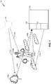
- FIG. 1 is a diagram illustrating a scene, an image capture device, and various target objects in the scene and within a field of view of the image capture device, in accordance with an exemplary implementation.
- the image capture device (“camera”) 102 may include a near infrared (“NIR”) sensor 104 and an "artificial NIR light source (“NIR source”) 105, for example, a flash light source or another artificial light source on or coupled to the camera 102.
- the NIR source 105 may be referred to as a first NIR source.
- the field of view (“FOV”) of the camera 102 may include target objects 108a-c, including a bush 108a, a person 108b, and a tree 108c.
- the scene 100 may further include an external NIR source 110 independent from the camera 102, the example, a natural light source (the sun) or an artificial light source not on the camera 102.
- Reflected light 106a-c represents paths of NIR light reflected off of the target objects 108a-c, respectively.
- Emitted light 112a represents paths of NIR light emitted from the external NIR source 110.
- Emitted light 112b represents some paths of NIR light emitted from the NIR source 105.
- the NIR sensor 104 may sense NIR light (or NIR signals), for example via optics of the camera 102 not shown in this figure, and thus capture an image of the FOV of the camera 102 based on the sensed NIR light.
- the NIR light sensed by the NIR sensor 104 may include the reflected light 106a-c which was emitted from NIR source 105 and reflected from the target objects 108a-c, emitted light 112a from the external NIR source 110 and/or emitted light 112b from the NIR source 105, or a combination of both the reflected light 106a-c and the emitted light 112a and 112b.
- the NIR sensor 104 may absorb the emitted light 112a and 112b emitted from the external NIR source 110 and NIR source 105 directly or after it reflects off of the target objects 108a-c within the FOV of the camera 102.
- the emitted light 112 NIR source 105 may be a flash, emitting emitted light 112a when the camera 102 is used to capture an image using the NIR sensor 104.
- the NIR source 105 may provide constant illumination for the duration of a NIR sensor 104 sensing period.
- the NIR sensor 104 and the NIR source 105 may be two components that are configured to operate together or may be integrated into a single component.
- the NIR sensor 104 may be configured to generate an image of the FOV based on the absorbed light.
- the NIR sensor 104 may include one or more NIR sensing elements (which may be referred to as pixels herein) as will be described in further detail below.
- the external NIR source 110 may function independently of the camera 102 (for example, as a constantly illuminated source, for example, the sun) or may function dependent upon the camera 102 (for example, as an external flash).
- the external NIR source 110 may comprise an exterior light that constantly emits the emitted light 112 within the FOV of the camera 102 or in a portion of the FOV of the camera 102.
- the camera 102 may include a device capable of capturing a still or moving image, regardless of format (digital, film, etc.) or type (video camera, still camera, web camera, etc.).
- the camera 102 may determine a distance to or depth of a target scene or a target object (that is, an object in the target scene) based on one or more signals received from the NIR sensor 104.
- target object will refer to both a target scene and a target object in the context of being subject matter on which the camera is focused.
- the emitted light 112 represent the paths light from the NIR source 105 and the external NIR source 110 may propagate. from the NIR source 105 and the external NIR source 110 to the target objects 108a-c.
- the embodiment of Figure 1 shows the NIR sensor 104 receiving the reflected light 106a-c from the target objects 108a-c within the FOV of the camera 102. As shown, the target objects 108a-c may be at various depths from the camera 102. However, in some embodiments, the target objects 108a-c may be at a single depth from the camera 102. Target objects 108a-c each reflect reflected light 106a-c representing NIR light reflecting off of the target objects 108a-c.
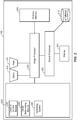
- Figure 2 is a block diagram illustrating an example of one embodiment of an image capture device using an NIR sensor.
- Figure 2 illustrates a high-level block diagram of an example of some embodiments of a camera 102 having a set of components including an image processor 220 linked to an optics 215, a flash (or other light source) 216, and to modules for operating the camera 102.
- the image processor 220 may also be in communication with a working memory 205, a memory 230, and a device processor 250, which in turn may be in communication with electronic storage module ("storage") 210, and a display 225 (for example an electronic or touchscreen display).
- a single processor may comprise both the image processor 220 and the device processor 250 instead of two separate processors as illustrated in Figure 2 .
- Some embodiments may include three or more processors. In some embodiments, some of the components described above may not be included in the camera 102 or additional components not described above may be included in the camera 102. In some embodiments, one or more of the components described above or described as being included in the camera 102 may be combined or integrated into any other component of the camera 102.
- the camera 102 may be, or may be part of, a cell phone, digital camera, tablet computer, personal digital assistant, laptop computer, personal camera, action camera, mounted camera, connected camera, wearable device, automobile, drone, or the like.
- the camera 102 may also be a stationary computing device or any device in which depth sensing would be advantageous.
- a plurality of applications may be available to the user on the camera 102. These applications may include traditional photographic and video applications, high dynamic range imaging, panoramic photo and video, or stereoscopic imaging such as 3D images or 3D video.
- the camera 102 includes the optics/lens ("optics") 215 for capturing images of target objects and/or scenes.
- the optics 215 may include at least one sensor and at least one optical imaging component that focuses light received from the FOV of the camera 102 (for example, the FOV of the optics 215) onto the at least one sensor.
- the at least one sensor may comprise a CMOS or CCD sensor, such as the NIR sensor 104 described in relation to Figure 1 .
- the camera 102 may include more than one optics 215 or more than one sensor within the optics 215.
- the optics 215 may be coupled to the image processor 220 to transmit a captured image to the image processor 220. In this embodiment, signals to and from the optics 215 are communicated through the image processor 220.
- the camera 102 may include the flash 216.
- the camera 102 may include at least one flash 216.
- the flash 216 may include, for example, a flash bulb, a reflector, a geometric light pattern generator, an LED flash, or a NIR light source (such as NIR source 105 as referenced in Figure 1 ).
- the image processor 220 can be configured to receive signals from and transmit signals to the flash 216 to control the flash.
- the image processor 220 is connected to the memory 230 and the working memory 205.
- the memory 230 may be configured to store the capture control module 235, the depth determining module 240, and the operating system 245. Additional modules may be included in some embodiments, or fewer modules may be included in some embodiments. These modules may include instructions that configure the image processor 220 to perform various image processing and device management tasks.
- the working memory 205 may be used by the image processor 220 to store a working set of processor instructions or functions contained in one or more of the modules of the memory 230.
- the working memory 205 may be used by the image processor 220 to store dynamic data created during the operation of the camera 102 (e.g., one or more target object depth measurements, etc.). While additional modules or connections to external devices or hardware may not be shown in this figure, they may exist to provide other exposure and focus adjustment and estimation options or actions.
- the image processor 220 may be configured by or may operate in conjunction with several modules stored in the memory 230.
- the capture control module 235 may include instructions that control the overall image capture functions of the camera 102.
- the capture control module 235 may include instructions that configure the image processor 220 to capture raw image data of the target object using the optics 215.
- the capture control module 235 may also be configured to activate the flash 216 when capturing the raw image data.
- the capture control module 235 may be configured to store the captured raw image data in the electronic storage module 210 or to display the captured raw image data on the display 225.
- the capture control module 235 may direct the captured raw image data to be stored in the working memory 205.
- the capture control module 235 may call one or more of the other modules in the memory 230, for example the depth determining module 240, to perform a depth determination technique on images captured by the optics 215 and output a depth map or depth information to image processor 220.
- the depth determining module 240 may comprise instructions that configure the image processor 220 to perform depth determination, depth matching, or depth mapping techniques on captured image data.
- the optics 215 may capture a view of the target objects ( Figure 2 ).
- the depth determining module 240 may configure the image processor 220 to perform a depth determining operation on the target object(s) 108 of the FOV of the optics 215.
- the depth determination may include disparity matching, or any other depth determining operation.
- the operating system 245 may configure the image processor 220 to manage the working memory 205 and the processing resources of camera 102.
- the operating system 245 may include device drivers to manage hardware resources such as the optics 215 and the flash 216. Therefore, in some embodiments, instructions contained in the processing modules discussed above and below may not interact with these hardware resources directly, but instead interact with this hardware through standard subroutines or APIs located in the operating system 245. Instructions within the operating system 245 may then interact directly with these hardware components.
- the operating system 245 may further configure the image processor 220 to share information with the device processor 250.
- the operating system 245 may also include instructions allowing for the sharing of information and resources between the various processing modules of the camera 102.
- the device processor 250 may be configured to control the display 225 to display the captured image, or a preview of the captured image, to a user.
- the display 225 may be external to the camera 102 or may be part of the camera 102.
- the display 225 may also be configured to provide a view finder displaying a preview image for a use prior to capturing an image, or may be configured to display a captured image stored in memory or recently captured by the user.
- the display 225 may include a panel display, for example, an LCD screen, an LED screen, or other display technologies, and may implement touch sensitive technologies.
- the device processor 250 may also be configured to receive an input from the user.
- the display 225 may also be configured to be a touchscreen, and thus may be configured to receive an input from the user.
- the user may use the display 225 to input information that the device processor 250 may provide to the depth determining module 240.
- the user may use the display 225 to select a target object from the FOV shown on or in the display 225.
- the device processor 250 may receive that input and provide it to the depth determining module 240, which may use the input to select specific objects for the depth determination operations.
- the device processor 250 may be configured to control the one or more of the processing modules in the memory 230 or to receive inputs from one or more of the processing modules in the memory 230.
- the device processor 250 may write data to the electronic storage module 210, for example data representing captured images. While the electronic storage module 210 is represented graphically as a traditional disk device, in some embodiments, the electronic storage module 210 may be configured as any storage media device.
- the electronic storage module 210 may include a disk drive, such as a floppy disk drive, hard disk drive, optical disk drive or magneto-optical disk drive, or a solid state memory such as a FLASH memory, RAM, ROM, and/or EEPROM.
- the electronic storage module 210 can also include multiple memory units, and any one of the memory units may be configured to be within the camera 102, or may be external to the camera 102.
- the electronic storage module 210 may include a ROM memory containing system program instructions stored within the camera 102.
- the electronic storage module 210 may also include memory cards or high speed memories configured to store captured images which may be removable from the camera.
- Figure 2 depicts the camera 102 having separate components to include the device processor 250, the image processor 220, and the electronic storage module 210 (among other components), in some embodiments these separate components may be combined in a variety of ways to achieve particular design objectives.
- the memory components for example, electronic storage module 210 or working memory 205 or memory 230
- processor components for example, image processor 220 and/or device processor 250
- Figure 2 illustrates a number of memory components, including the memory 230 comprising several processing modules and a separate memory comprising a working memory 205
- different memory architectures may be utilized.
- a design may utilize ROM or static RAM memory for the storage of processor instructions implementing the modules contained in memory 230.
- the processor instructions may be loaded into RAM to facilitate execution by the image processor 220.
- working memory 205 may comprise RAM memory, with instructions loaded into working memory 205 before execution by the image processor 220.
- one or more of the processing modules may be software stored in the memory 230 or may comprise a hardware system combined with the software components.
- functions associated above with one of the image processor 220 and the device processor 250 may be performed by the other of the image processor 220 and the device processor 250 or both the image processor 220 and the device processor 250, though not described as such above.
- Figure 3A and 3B each include a graph indicating spectral responses of a frontside illumination (FSI) device ( Figure 3A ) and a back-side illuminated (BSI) image sensor ( Figure 3B ), highlighting the NIR wavelength region and the associated ability for the respective devices to realize signals having wavelengths within the NIR region.
- Figure 3A and 3B highlight the NIR wavelength region and the associated ability for the respective devices to realize signals having wavelengths within NIR regions 305 and 355, respectively.
- a spectral response can be characterized by a ratio of current generated by a photodiode in response to its exposure to light. The spectral response may also be expressed as a Quantum efficiency, as shown in the graphs illustrated in Figures 3A and 3B along the y-axis.
- Figure 3A is a graph 300 illustrating an example of Quantum efficiency of an FSI device, for each of red light 310, green light 315, and blue light 320, relative to the received wavelength.
- a thickness of the FSI device may vary.
- the wavelength of the received signal from 400 nanometers (nm) to 1100nm.
- the term "realized" in relation to the received light may correspond to an ability of the sensor to convert the received light to a current corresponding to a wavelength of the received light.
- the graph 300 also shows a window from approximately 760nm to approximately 960nm, indicating the near-infrared ("NIR") light region 305.
- NIR near-infrared
- the light is received with greater than 50% efficiency at under 600nm, but as the wavelength of the received light increases (moving along the x-axis of the graph 300 to the right), the Quantum efficiency of the FSI devices decreases. As will be discussed further below, this may be due to the thickness of a photodetector region of the FSI device in relation to the wavelength of the NIR light.
- Figure 3B is a graph 350 illustrating an example of the Quantum efficiency of a back side illuminated (“BSI") device(or sensor) for each of red light 370, green light 365, and blue light 360, relative to the received wavelength.
- BSI back side illuminated
- a thickness of the BSI device may vary.
- the wavelength of the received signal from 400nm to 1100nm.
- the graph 350 also shows a window from approximately 760nm to approximately 960nm, indicating the NIR light region 355.
- the light is received with greater than 50% efficiency at under 600nm, but as the wavelength of the received light increases (moving along the x-axis of the graph 350 to the right), the Quantum efficiency of the BSI sensor decreases. As will be discussed further below, this may be due to the thickness of a photodetector region of the BSI sensor in relation to the wavelength of the NIR light.
- the FSI device is generally more efficient for converting received light to current.
- the FSI device has a maximum efficiency of approximately 30%, while the BSI sensor maximum is approximately 20% in the NIR region 355.
- the FSI device may provide higher NIR (and greater wavelength) Quantum efficiencies than the BSI image sensor, the FSI may not be compatible with 3D stacked sensor (and similar) technology and practices, and thus may not be a suitable replacement BSI image sensors in some applications (for example due to size constraints, etc.).
- the behavior of the FSI and BSI devices with regards to their lack of efficiency at converting received light to current is independent of pixel size.
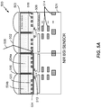
- Figure 4 shows an example not forming part of the claimed invention of a cross section of a 3D stacked BSI sensor (including four pixels) incorporating metal reflectors to cause light to reflect back through a photodetector region and improve spectral response of the BSI image sensor.
- the BSI sensor may form a compacted depth sensing camera module that functions effectively in mobile applications.
- the cross section of the BSI sensor 400 shows four sensor pixels 401a, 401b, 401c and 401d. For clarity, only the structure of pixel 401a is described, each of the sensor pixels 401a-d having a similar structure.
- Pixel 401a includes a microlens 402 and an n-type photodetector region (photodetector region) 404, a metal reflector 408, a transfer gate 410, a p-type photodetector region 412, three rows of metal interconnects/layers 414, a photodetector isolation region 416 configured to suppress pixel signal crosstalk, and a substrate portion 421 within which the transfer gate 410 and the metal interconnects/layers 414 and metal reflector 408 are disposed.
- the BSI sensor includes a high refractive index film between the photodetector region 404 and the substrate portion 421.
- the high refractive index film may be configured to prevent at least a portion of light from propagating from the photodetector region 404 to the substrate portion 421.
- the BSI sensor also may include an antireflection layer 403 that is configured to allow light to pass from the microlens 402 through the antireflection layer 403 and into the photodetector region 404, and prevents at least some light from propagating from the photodetector region 404 to the microlens 402.
- the photodetector isolation region 416 suppresses pixel signal crosstalk.
- neighboring pixels of the BSI sensor 400 may share the substrate portion and one or more of a reset transistor, a selection transistor, and an amplifying transistor (not shown in this figure).
- the metal interconnects/layers 414 and metal reflector 408 may comprise one or more portions of the reset, selection, and amplifying transistors.
- light 406 (for example NIR light) enters the photodetector region 404 from the top of the figure.
- the light 406 may pass through the microlens 402, which focus the light 406 and directs it to propagate through the photodetector region 404.
- the photodetector region 404 may convert at least a portion of the light 406 into current.
- the photodetector region 404 of each pixel may be formed from silicon and may be less than 3 microns thick.
- Light 406, having a wavelength in the NIR or longer range, may have a penetration depth that exceeds the thickness of the photodetector region 404. For example, the penetration depth of the light 406 into silicon may be beyond 5 microns.
- the photodetector region 404 may not effectively convert the light 406.
- the full energy from the light 406 may not be converted to current.
- the photodetector region 404 may be too thin to convert all of the light 406 to current, as a portion of the light 406 (when in the NIR or greater wavelength range) may pass through the photodetector region 404 without being converted to current.
- a portion of the energy in the light 406 that is not converted to current can be lost as it may continue to penetrate the substrate of the BSI sensor without being converted to electricity.
- the substrate 421 BSI sensor may include multiple metal interconnects or metal layers.
- the metal reflector (“M1") 408 and metal interconnects/layers (“M2-M4") 414 which may include wiring or transistors internal to the BSI sensor 400.
- the metal reflector 408 and the metal interconnects/layers 414 may be located at various depths within the substrate of the BSI sensor 400.
- the metal interconnects or metal layers may serve as power supply, ground, clock, and video signal lines, etc.
- the metal reflector 408 may be the top most metal layer (closest to the photodetector region 404). In some examples, the metal reflector 408 is wider than the M2-M4metal interconnects/layers 414. This is because the metal reflector M1 408 may be configured to reflect the light 406, which passes through the photodetector region 404 without being converted to current, back through the photodetector region 404. The metal reflector 408 may be located adjacent to the photodetector region 404 and may be closest to the photodetector region 404 compared to other metal interconnects/layers 414 illustrated in Figure 4 . In some examples the metal reflector 408 includes one or more metal layers.
- the metal reflector 408 may be fewer components between the metal reflector 408 and the photodetector region 40, compared to the other metal interconnects/layers 414.
- the metal reflector 408 is configured to be wider than the other metal interconnects/layers 414to increase the amount of light reflected by the metal reflector 408. This may minimize the amount of the light 406 that is lost due to reflections off of, or absorption by, other components within the substrate 421 of the BSI sensor.
- the metal reflector 408 may be the same width as, or substantially the same with as, the photodetector region 404 for each pixel of the BSI image sensor.
- the metal reflector 408 may be 95% or greater of the width as the photodetector region 404 of a pixel.
- the metal reflector 408 may be 90% or greater of the width as the photodetector region 404 of a pixel.
- the metal reflector 408 may be 85% or greater of the width as the photodetector region 404 of a pixel.
- the metal reflector 408 may be located as close to the photodetector region 404 as possible, further minimizing the light 406 that is lost within the substrate of the BSI sensor 400.
- the substrate of the BSI sensor 400 is formed from a material with a low refraction (for example, glass, having a refractive index of approximately 1.4)
- the distance between the photodetector region 404 and the metal reflector 408 may be increased with minimal penalty.
- the metal reflector 408 may not be formed within the photodetector region 404 because the metal reflector 408 has a lower melting point than the silicon material of the photodetector region 404. The metal reflector 408 may thus contaminate the photodetector region 404 if it is embedded within the photodetector region 404.
- Reflecting the light 406 back through the photodetector region 404 may allow the photodetector region 404 to increase the amount of the light 406 converted to power regardless of the wavelength of the light 406 (for example, where the light 406 has a penetration depth of less than twice the thickness of the photodetector region 404 so that light that passes through the photodetector region for a second time is absorbed).
- the light 406 may include NIR light having a penetration depth into silicon photodetectors of 5 microns
- the metal reflector 408 may reflect the NIR light back through the photodetector region 404.
- this reflection of the light406 back through the photodetector region 404 may allow the photodetector region 404 to convert to current the remaining amount the light 406 that was not converted to current on the first pass through the photodetector region 404 when it travels a distance of 2 microns through the photodetector region 404.
- the metal reflector 408 effectively doubles the thickness of the photodetector region 404. The ability for the photodetector region 404 to convert the light 406 to current increases the quantum efficiency of the BSI sensor 400.
- Figure 5A is an illustration of an embodiment of the 3D stacked BSI sensor of Figure 4 further incorporating a reflective grating to cause light to reflect back through the photodetector region and improve spectral response of the BSI image sensor.
- the BSI sensor 500 shown in Figure 5A includes many of the same components as shown and discussed in relation to Figure 4 , and such components need not be discussed again here.
- the reflective structures are a reflective "grating" 518 positioned within the photodetector region 504 adjacent to and in the proximity of a substrate 521 of the BSI sensor 500.
- the grating 518 may be a set of structures that are periodically arranged, some examples of which are illustrated in Figures 5B, 5C and 5D .
- the structures are randomly arranged, and such structures can have different reflection characteristics compared with structures that are periodically arranged.
- the gratings 518 are formed of a silicon dioxide material. The grating 518 may reflect the light 506 within the photodetector region 504 of the BSI sensor 500 without causing the reflected light to impact or interfere with neighboring pixels of the BSI sensor 500.
- the reflective structure metal reflector 508
- the light reflecting off of the metal reflector 508 may reflect into a neighboring photodetector region 504 due to lack of physical barriers or dividers between the substrate regions of neighboring shared pixels. Dividing or separating the photodetector regions 504 using photodetector isolation regions 516 lowers the chances that the light reflecting off of a reflective structure (for example, grating 518) located within a first photodetector region 504a will propagate to a second photodetector region 504b adjacent to the first photodetector region 504a.
- the photodetector isolation regions 516 may comprise the same material(s) as the reflective gratings 518, and the gratings 518 may be formed of or coated with the similar materials as metal reflectors 508 and 514.
- the grating 518 may comprise (e.g., be formed of or coated by) one or more of silver, copper, gold, aluminum, platinum, rhodium, and chromium. Each of these materials may reflect over 60% of light within or above the NIR wavelength range. Additionally, the BSI sensor 500 manufacturing process may already use these materials, so there may be only a nominal cost to the process to add these materials in the form of the grating 518.
- the manufacturing process of a BSI sensor may incorporate the construction of the gratings 518 into each photodetector region 504.
- the manufacturing process of a BSI sensor may be modified to incorporate the construction of the metal reflector 508 into each photodetector region 504 or into each substrate 521 below the photodetector region 504.
- the construction of the BSI sensor may be modified to incorporate the construction of either or both the gratings 518 into each photodetector region 504 and the construction of the metal reflector 508 below the photodetector region 504 within the substrate 521.
- Such leveraging of the existing construction process and existing pixel physical design and manufacturing may allow the modification of the BSI sensor discussed with no additional layers (for example, no additional mask layer) or steps, as the construction of the metal reflector 408 or the gratings 518 may be integrated into existing construction process steps.
- the BSI sensor 500 includes an anti-reflection layer 503 shown between the microlenses 502 and the photodetector regions 504.
- the anti-reflection layer 503 may be formed such that light may propagate through the microlens 502 and through the anti-reflection layer 503 but light does not pass through (or only a minimum amount of light passes through) the anti-reflection layer 503 from the photodetector region 504 to the microlens 502.
- Such modifications provide for an increase in the resolution of the Quantum efficiency of the BSI sensor pixels and increases in depth map coding accuracy, distance range, and non-linearity of these pixels.
- the gratings 518 may cause the light 506 to reflect within the photodetector region 504.
- the grating 518 may better confine the incident light, especially light of a longer wavelength (for example, wavelengths greater than 700 nm), inside a grating cavity (a cavity formed between adjacent gratings) so as to enhance charge collection efficiency. Accordingly, adjacent gratings may cause the light 506 to reflect off of each other within the grating cavity, extending a path of the light 506 within the photodetector region 504.
- the distance d between consecutive gratings may be approximately 0.4 micron.
- the gratings are spaced from between 0.2 and 0.4 microns apart.
- a size of the gratings may be adjusted based at least in part on the wavelength of the signal or light being absorbed by the photodetector region. In some embodiments, the spacing, size, and/or shape of the gratings are not consistent throughout the photodetector region.
- the gratings 518 may be used in combination with the reflective metal reflectors 508.
- Embodiments illustrated in Figures 5B-5D show examples that include a high refractive index film 524 deposited on top of the gratings 518.
- the high refractive index film 524 may serve to improve the trapping of light within the grating cavities formed for neighboring gratings 518.
- the high refractive index film 524 may comprise a material having a higher refractive index than glass (for example, greater than 1.4).
- the high refractive index film 524 may comprise one of Si 3 N 4 , HfO 2 , or Ta 2 O 5 , among others.
- Figure 5B is an illustration of an embodiment of the 3D stacked BSI sensor of Figure 5A including a single period reflective grating.
- the single periodic grating 518b may include one or more structures having a height and width, and that extend along a length of the photodetector region 504.
- "Single period" in this example indicates that the gratings 518 are periodic along a single axis of the photodetector region 504 along the width of the photodetector region 504 (Si-Detector) in Figure 5B .
- gaps or spaces 520a between neighboring gratings may exist in only one axis of the plane of the single periodic grating 518b, for example, extending into the page relative to the orientation of Figure 5A and 5B .
- Distance 522a corresponds to the width of the single periodic grating 518b along the periodic axis across the width of the photodetector region 504.
- a distance 522b corresponds to the height of the single periodic grating 518b along the height of the photodetector region 504.
- FIG. 5C is an illustration of an embodiment of the 3D stacked BSI sensor of Figure 5A including a bi-periodic reflective grating having a different shape.
- the bi-periodic grating 518c illustrated in Figure 5C may include a plurality of structures having a height, width, and length that are arranged in an array within a photodetector region 504.
- "Bi-periodic" is in reference to gratings being periodic along two axis of the photodetector region 504 (for example, along the width and the depth of the photodetector region 504 (Si-Detector) in Figure 5C ).
- gaps 520a and 520b may exist in both axes of the plane of the grating 518, as shown in Figure 5C .
- the gaps 520a may include the gaps or spaces along the width of the photodetector region 504 as shown in Figure 5C
- the gaps 520b may include the gaps or spaces that divide individual gratings 518 as they extend into the page.
- the gaps 520a and 520b may have the same distance or may be different distances.
- Figure 5C depicts the bi-periodic grating 518c as having a cylindrical shape instead of a rectangular or cubic shape as in Figures 5A , 5B, and 5D ; however, in some examples the bi-periodic grating 518c may include rectangular structures, square structures, or structures of a different shape.
- Distance 522a corresponds to the width of the bi-periodic grating 518c along the periodic axis across the width of the photodetector region 504.
- a distance 522b corresponds to the height of the bi-periodic grating 518c along the height of the photodetector region 504.
- each of the grating structures in the bi-periodic grating 518c may be located in the same plane within the photodetector region 504, while in other embodiments, the grating 518 may be located in various planes within the photodetector region 504 (not shown). In various embodiments, the bi-periodic grating 518c may have different dimensions or be made from different reflective materials.
- FIG 5D is an illustration of another embodiment of the 3D stacked BSI sensor of Figure 5A including a bi-periodic reflective grating having a different bi-periodic layout.
- the bi-periodic grating 518d may include a plurality of structures having a height, width, and length that are arranged in an array within the photodetector region 504, where alternating rows of gratings are offset to form a "checkerboard" type structure.
- the bi-period may suggest that the gratings are periodic along two axes of the photodetector region 504 (along the width and the depth of the photodetector region 504 (Si-Detector) in Figure 5D ).
- gaps 520a and 520b may exist in both axes of the plane of the reflective grating structure 518, as shown in Figure 5D .
- the gaps 520a may include the gaps or spaces along the width of the photodetector region 504 as shown in Figure 5D
- the gaps 520b may include the gaps or spaces that separate individual gratings as they extend into the page.
- the gaps 520a and 520b may have the same distance or may be different distances.
- Distance 522a corresponds to the width of each bi-periodic grating 518d along the periodic axis across the width of the photodetector region 504.
- a distance 522b corresponds to the height of the bi-periodic grating 518d along the height of the photodetector region 504.
- Figure 5D also depicts the grating 518 as having a cubic or rectangular shape as in Figures 5A and 5B .
- each of the gratings of the bi-periodic grating 518d may be placed in the same plane within the photodetector region 504, while in other embodiments, the gratings of the bi-periodic grating 518d may be placed in various planes within the photodetector region 504 (not shown).
- the bi-periodic grating 518d may have different dimensions or be formed of different reflective materials.
- the BSI devices having the structures shown in Figures 4-5D may be formed via front end of line (FEOL) processes.
- the FEOL process may include all manufacturing processes of the BSI device up to (but not including) the back end of line (BEOL) processes.
- the FEOL processes may include forming individual devices that are formed on or from a semiconductor material.
- the photodetector region 404 and 504, the photodetector isolation regions 416 and 516, and the grating 518 may be formed during the FEOL processes. Integrating the forming of the grating 518 with the FEOL process may simplify the formation of the grating 518 and reduce the overall cost of incorporating such structures in the photodetectors.
- shallow trench isolation or similar processes may be used to isolate the devices formed on or from the semiconductor material, such as the photodetector regions 504.
- the photodetectors may be isolated using implant isolation, for example using p+ isolation.
- the BEOL processes may involve connecting the structures and devices formed during the FEOL processes with wiring and/or metal layers.
- the BEOL processes may involve forming the metal layers M1, M2, M3, and M4 and the surround substrate in which they are located.
- the antireflection and microlens layers are applied after the FEOL and BEOL processes are complete.
- the high refractive index film 524 may be formed during either the FEOL or BEOL processes, as the high refractive index film 524 may be positioned between the photodetector 404/504 material and the substrate of the metal layers region.
- the grating 518 use the same formation procedure to form is either a single period or bi-periodic.
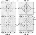
- Figures 6A-6D include four top down views of the shared pixels BSI sensor of Figures 4 and 5 .
- the Figures 6A -6D as shown do not include the microlens 402 ( Figure 4 ).
- Each of the Figures 6A-6D show a 2x2 pixel array and associated shared transistor regions.
- the NIR light that penetrates the silicon photodetector regions (photodetector regions) 604 may be eventually lost or may dissipate as it continues to penetrate the photodetector regions 604.
- Figure 6A shows the 2x2 pixel array without either the metal reflector 408 ( Figure 4 ) or the grating 518 ( Figure 5 ).
- Figure 6B shows the 2x2 pixel array with only the metal reflector 408.
- Figure 6C shows the 2x2 pixel array with only the grating 518.
- Figure 6D shows the 2x2 pixel array with both the metal reflector 408 and the grating 518.
- Each of the Figures 6A-6D also show shared reset and source/follower amplifiers. In these figures, the light entering the BSI sensor may come from inside the page.
- Figure 6A shows only the 2x2 pixel architecture including the transfer gates 610 (corresponding to transfer gate 410 of Figure 4 ), photodetector (or active or pixel transistor) regions 604 (corresponding to photodetector region 404 of Figure 4 ), and contacts 620 (p+ substrate tie (diamond) to combat ground bouncing (for example, providing a solid ground), while the square is the n+ contact).
- the contacts 620 may comprise points of contact between different layers of the BSI image sensor.
- the horizontal regions below each 2x2 pixel architecture comprises the transistors and associated components that are shared by the 2x2 structure above.
- Figure 6B shows the 2x2 pixel architecture of Figure 6A with the added metal reflectors 608 (corresponding to metal reflectors 508) for each of the photodetector regions 604.
- the metal reflectors 608 may be formed to be substantially the same size as the photodetector region 604. In other words, the metal reflectors 608 may have the same, or substantially the same, cross-sectional area as a sensor pixel. Accordingly, the area of the metal reflector 608 may be smaller than the area of the photodetector region 604 as seen in Figure 6B .
- the metal reflectors 608 also overlap with the transfer gates (or polygate region) 610 of each of the pixels. However, in some examples, the metal reflectors 608 may not overlap with the transfer gates 610 of each of the pixels.
- Figure 6C includes the 2x2 pixel architecture of Figure 6A with the added array of gratings 618 (corresponding to grating 518) for each of the photodetector regions 604.
- the array of gratings 618 may be configured to cover substantially all portions of the photodetector region 604.
- the array of gratings 618 may be configured to have more or less area of the photodetector region 604 covered.
- the array of gratings 618 may comprise any other shape or may comprise a plurality of shapes.
- the array of reflective grating structures may be configured to overlap with the transfer gates 610 of the pixels.
- Figure 6D includes the 2x2 pixel architecture of Figure 6A with the added metal reflectors 608 of the Figure 6B and the array of gratings 618 of Figure 6C .
- the metal reflectors 608 and the array of gratings 618 may be configured to cover substantially the entire photodetector region 604 as shown.
- the high refractive index film may overlap the gratings 618 and the STI region shown by the photodetector regions 604.
- FIG. 7 is a flowchart illustrating an example of a method of manufacturing a BSI image sensor, according to some embodiments.
- the method 700 begins at block 702 and proceeds to block 704.
- the method 700 of manufacturing the BSI image sensor forms one or more photodetector regions having an active region.
- the one or more photodetector regions may correspond to the photodetector region 404 of FIG. 4 .
- the method 700 then proceeds to block 706, where it forms one or more reflector structures configured to confine the light within the reflector cavities.
- the reflector structures may comprise the one or more grating structures 518 ( FIG. 5 ), and the reflector cavities may be the spaces between the grating structures 518, e.g., gaps 520.
- the method 700 then proceeds to block 708, where it forms one or more metal structures configured to interconnect components of the photodetector region.
- These one or more metal structures may comprise any of the metal components that are formed within the substrate portion 421 ( FIG. 4 ), such as the transfer gates, the metal layers 414, metal reflector 408, etc.
- the method 700 proceeds to block 710, where the one or more metal structures are isolated from each other with a dielectric material region, which may correspond to the substrate portion 421.
- the antireflective layer may correspond to the antireflection layer 403 of FIG. 4 .
- the method 700 proceeds to block 714, where one or more microlenses are formed and configured to collect more light into the one or more photodetector regions.
- the microlenses may correspond to the microlenses 402 of FIG. 4 .
- the method 700 ends at block 716.
- the blocks of method 700 indicated above may be performed in any order. Alternatively, the method 700 may include additional blocks not shown here or may exclude blocks shown here.
- FIG. 8 is a flowchart illustrating an example of a method of capturing an image via an IR sensor apparatus, according to some embodiments.
- the method 800 begins at block 802 and proceeds to block 804.
- the method 800 focuses received light onto a photodetector region of a pixel.
- the photodetector region may correspond to the photodetector region 404 of FIG. 4 above, and the pixel may correspond to a structure comprising the photodetector region 404 and any associated substrate and metal interconnections, isolated from neighboring photodetector regions 404 and metal interconnections.
- the light is focused via the microlenses 402 of FIG. 4 .
- the method 800 then proceeds to block 806, where the method 800 converts the received light into current via the photodetector region.
- the method 800 then proceeds to block 808, where a path length of the received light is increased through at least a portion of the photodetector region via an array of one or more reflector structures.
- the reflector structures may correspond to the gratings 518 ( FIG. 5 ). Increasing the path length may allow the photodetector region to convert a larger amount of the received light into current.
- the reflector structures may be combined with the metal reflector 508. The method 800 then ends at block 810.
- determining encompasses a wide variety of actions. For example, “determining” may include calculating, computing, processing, deriving, investigating, looking up (e.g., looking up in a table, a database or another data structure), ascertaining and the like. Also, “determining” may include receiving (e.g., receiving information), accessing (e.g., accessing data in a memory) and the like. Also, “determining” may include resolving, selecting, choosing, establishing and the like. Further, a "channel width” as used herein may encompass or may also be referred to as a bandwidth in certain aspects.
- a phrase referring to "at least one of' a list of items refers to any combination of those items, including single members.
- "at least one of: a, b, or c” is intended to cover: a, b, c, a-b, a-c, b-c, and a-b-c.
- any suitable means capable of performing the operations such as various hardware and/or software component(s), circuits, and/or module(s).
- any operations illustrated in the Figures may be performed by corresponding functional means capable of performing the operations.
- an interface may refer to hardware or software configured to connect two or more devices together.
- an interface may be a part of a processor or a bus and may be configured to allow communication of information or data between the devices.
- the interface may be integrated into a chip or other device.
- an interface may comprise a receiver configured to receive information or communications from a device at another device.
- the interface e.g., of a processor or a bus
- an interface may comprise a transmitter configured to transmit or communicate information or data to another device.
- the interface may transmit information or data or may prepare information or data for outputting for transmission (e.g., via a bus).
- DSP digital signal processor
- ASIC application specific integrated circuit
- FPGA field programmable gate array signal
- PLD programmable logic device
- a general purpose processor may be a microprocessor, but in the alternative, the processor may be any commercially available processor, controller, microcontroller or state machine.
- a processor may also be implemented as a combination of computing devices, e.g., a combination of a DSP and a microprocessor, a plurality of microprocessors, one or more microprocessors in conjunction with a DSP core, or any other such configuration.
- the functions described may be implemented in hardware, software, firmware, or any combination thereof. If implemented in software, the functions may be stored on or transmitted over as one or more instructions or code on a computer-readable medium.
- Computer-readable media includes both computer storage media and communication media including any medium that facilitates transfer of a computer program from one place to another.
- a storage media may be any available media that can be accessed by a computer.
- such computer-readable media can comprise RAM, ROM, EEPROM, CD-ROM or other optical disk storage, magnetic disk storage or other magnetic storage devices, or any other medium that can be used to carry or store desired program code in the form of instructions or data structures and that can be accessed by a computer.
- Disk and disc includes compact disc (CD), laser disc, optical disc, digital versatile disc (DVD), floppy disk and Blu-ray disc where disks usually reproduce data magnetically, while discs reproduce data optically with lasers.
- computer readable medium may comprise non-transitory computer readable medium (e.g., tangible media).
- the methods disclosed herein comprise one or more steps or actions for achieving the described method.
- the method steps and/or actions may be interchanged with one another without departing from the scope of the claims.
- the order and/or use of specific steps and/or actions may be modified without departing from the scope of the claims.
- a storage media may be any available media that can be accessed by a computer.
- such computer-readable media can comprise RAM, ROM, EEPROM, CD-ROM or other optical disk storage, magnetic disk storage or other magnetic storage devices, or any other medium that can be used to carry or store desired program code in the form of instructions or data structures and that can be accessed by a computer.
- Disk and disc include compact disc (CD), laser disc, optical disc, digital versatile disc (DVD), floppy disk, and Blu-ray® disc where disks usually reproduce data magnetically, while discs reproduce data optically with lasers.
- certain aspects may comprise a computer program product for performing the operations presented herein.
- a computer program product may comprise a computer readable medium having instructions stored (and/or encoded) thereon, the instructions being executable by one or more processors to perform the operations described herein.
- the computer program product may include packaging material.
- modules and/or other appropriate means for performing the methods and techniques described herein can be downloaded and/or otherwise obtained by a user terminal and/or base station as applicable.
- a user terminal and/or base station can be coupled to a server to facilitate the transfer of means for performing the methods described herein.
- various methods described herein can be provided via storage means (e.g., RAM, ROM, a physical storage medium such as a compact disc (CD) or floppy disk, etc.), such that a user terminal and/or base station can obtain the various methods upon coupling or providing the storage means to the device.
- storage means e.g., RAM, ROM, a physical storage medium such as a compact disc (CD) or floppy disk, etc.
- CD compact disc
- floppy disk etc.
- any other suitable technique for providing the methods and techniques described herein to a device can be utilized.
Description
- This disclosure generally relates to providing improved or extended spectral response to near infrared light or signals in photographic and/or other image capture devices. More specifically, this disclosure relates to improving or extending the capabilities of a photodetector or photodiode to detect or receive a near infrared light or signal in an image sensor.
- Various configurations of imaging equipment may use near infrared (NIR) or longer wavelength light or signals for a variety of purposes. For example, human-machine interfaces (HMI) may utilize NIR or IR light or signals to communicate movement or other commands, for example gesture control. Machine "vision" systems may use NIR or longer wavelength light, allowing a machine or computer to "see" or otherwise optically view a scene or event. In many instances, one or more NIR sensors may sense the NIR signals, for example a back-side illuminated (BSI) sensor capable of detecting NIR signals. As advances in technology lead to the reduction in size of computers and other machines, the NIR sensors used in these devices may also become smaller. However, some image sensors may physically be unable to fully realize a NIR signal, for example due to the longer wavelength of NIR signals. Accordingly, systems and methods to allow these image sensors to more fully realize NIR signals in an imaging system would be beneficial.
- In
US 2015/0228689 A1 , there is described an imaging device including an image sensor having an array of image pixels. The array of image pixels includes one or more infrared pixels that are configured to detect infrared light. The infrared pixels include reflective structures for increasing quantum efficiency in the infrared spectral range. The reflective structures include first and second parallel structures formed on opposing sides of a photodiode in an infrared pixel. The reflective structures are partially transparent to infrared light and non-transparent to visible light. The reflective structures form an optical cavity so that infrared light that enters an infrared pixel is reflected back and forth between the reflective structures until it is absorbed by the photodiode in the infrared pixel. - In
JP 2009-088415 A - In
US 2012/0287297 A1 , there is described a solid-state imaging device that includes: - a photoelectric conversion device; a wire grid polarizer provided on the photoelectric conversion device; and a conductive film electrically connecting conductive layers provided in
- the photoelectric conversion device to the wire grid polarizer.
- In
US 2013/0113964 A1 , there is described a configuration in which a pixel detecting light having the longest wavelength in a picture element includes a protective film which is disposed on a photodiode at a surface side facing a light incident surface of a semiconductor substrate and a first diffraction grating portion which is disposed on the protective film and where columnar holes penetrating in a thickness direction are two-dimensionally arrayed. Diameter and array period of the holes are selected so that the first diffraction grating portion reflects light transmitting through a filter disposed on the pixel. - The invention is defined by the independent claims that form part of this disclosure.
- The systems, methods, and devices of the invention each have several aspects, no single one of which is solely responsible for its desirable attributes. Without limiting the scope of this invention as expressed by the claims which follow, some features will now be discussed briefly. After considering this discussion, and particularly after reading the section entitled "Detailed Description," one will understand how the features of the various embodiments of this invention provide advantages.
- The above-mentioned aspects, as well as other features, aspects, and advantages of the present technology will now be described in connection with various embodiments, with reference to the accompanying drawings. The illustrated embodiments, however, are merely examples and are not intended to be limiting. Throughout the drawings, similar symbols typically identify similar components, unless context dictates otherwise. Note that the relative dimensions of the following figures may not be drawn to scale.
-
Figure 1 is a diagram illustrating a scene, an image capture device, and various target objects in the scene and within a field of view of the image capture device, in accordance with an exemplary implementation. -
Figure 2 is a block diagram illustrating an example of one embodiment of an image capture device using an NIR sensor. -
Figure 3A and 3B each include a graph indicating spectral responses of a frontside illumination (FSI) device (Figure 3A ) and a back-side illuminated (BSI) image sensor (Figure 3B ), highlighting the NIR wavelength region and the associated ability for the respective devices to realize signals having wavelengths within the NIR region. -
Figure 4 shows an example not forming part of the claimed invention of a cross section of a 3D stacked BSI sensor (including four pixels) incorporating metal reflectors to cause light to reflect back through a photodetector region and improve spectral response of the BSI image sensor. -
Figure 5A is an illustration of an embodiment of the 3D stacked BSI sensor ofFigure 4 further incorporating a reflective grating to cause light to reflect back through the photodetector region and improve spectral response of the BSI image sensor. -
Figure 5B is an illustration of an embodiment of the 3D stacked BSI sensor ofFigure 5A including a single period reflective grating. -
Figure 5C is an illustration of an embodiment of the 3D stacked BSI sensor ofFigure 5A including a bi-periodic reflective grating having a different shape. -
Figure 5D is an illustration of another embodiment of the 3D stacked BSI sensor ofFigure 5A including a bi-periodic reflective grating having a different bi-periodic layout. -
Figures 6A-6D include four top down views of the shared pixels BSI sensor ofFigures 4 and5 . -
Figure 7 is a flowchart illustrating an example of a method of manufacturing a BSI image sensor, according to some embodiments. -
Figure 8 is a flowchart illustrating an example of a method of capturing an image via an IR sensor, according to some embodiments. - Various aspects of the novel systems, apparatuses, and methods are described more fully hereinafter with reference to the accompanying drawings. This disclosure may, however, be embodied in many different forms and should not be construed as limited to any specific structure or function presented throughout this disclosure. Rather, these aspects are provided so that this disclosure may be thorough and complete, and may fully convey the scope of the disclosure to those skilled in the art as set out in the appended claims. The scope of the disclosure is intended to cover aspects of the systems, apparatuses, and methods disclosed herein, whether implemented independently of, or combined with, any other aspect of the invention. For example, an apparatus may be implemented or a method may be practiced using any number of the aspects set forth herein.
- In some embodiments, the imaging systems described contain an IR sensor apparatus that may detect light within the visible range or near infrared ("NIR") or longer wavelength light (for example, infrared ("IR"), etc.). For clarity of description, "NIR light" will refer any light with a wavelength within the NIR range or having a wavelength longer than NIR light.
-
Figure 1 is a diagram illustrating a scene, an image capture device, and various target objects in the scene and within a field of view of the image capture device, in accordance with an exemplary implementation. As shown inFigure 1 , the image capture device ("camera") 102 may include a near infrared ("NIR")sensor 104 and an "artificial NIR light source ("NIR source") 105, for example, a flash light source or another artificial light source on or coupled to thecamera 102. TheNIR source 105 may be referred to as a first NIR source. The field of view ("FOV") of thecamera 102 may includetarget objects 108a-c, including abush 108a, aperson 108b, and atree 108c. Thescene 100 may further include anexternal NIR source 110 independent from thecamera 102, the example, a natural light source (the sun) or an artificial light source not on thecamera 102. Reflectedlight 106a-c represents paths of NIR light reflected off of thetarget objects 108a-c, respectively. Emittedlight 112a represents paths of NIR light emitted from theexternal NIR source 110. Emittedlight 112b represents some paths of NIR light emitted from theNIR source 105. - The
NIR sensor 104 may sense NIR light (or NIR signals), for example via optics of thecamera 102 not shown in this figure, and thus capture an image of the FOV of thecamera 102 based on the sensed NIR light. The NIR light sensed by theNIR sensor 104 may include thereflected light 106a-c which was emitted fromNIR source 105 and reflected from thetarget objects 108a-c, emittedlight 112a from theexternal NIR source 110 and/or emittedlight 112b from theNIR source 105, or a combination of both thereflected light 106a-c and the emittedlight NIR sensor 104 may absorb the emittedlight external NIR source 110 andNIR source 105 directly or after it reflects off of thetarget objects 108a-c within the FOV of thecamera 102. In some embodiments, the emitted light 112NIR source 105 may be a flash, emitting emittedlight 112a when thecamera 102 is used to capture an image using theNIR sensor 104. In other embodiments, theNIR source 105 may provide constant illumination for the duration of aNIR sensor 104 sensing period. In some embodiments, theNIR sensor 104 and theNIR source 105 may be two components that are configured to operate together or may be integrated into a single component. TheNIR sensor 104 may be configured to generate an image of the FOV based on the absorbed light. TheNIR sensor 104 may include one or more NIR sensing elements (which may be referred to as pixels herein) as will be described in further detail below. - As with the
NIR source 105, theexternal NIR source 110 may function independently of the camera 102 (for example, as a constantly illuminated source, for example, the sun) or may function dependent upon the camera 102 (for example, as an external flash). For example, theexternal NIR source 110 may comprise an exterior light that constantly emits the emitted light 112 within the FOV of thecamera 102 or in a portion of the FOV of thecamera 102. - In some embodiments, the
camera 102 may include a device capable of capturing a still or moving image, regardless of format (digital, film, etc.) or type (video camera, still camera, web camera, etc.). Thecamera 102 may determine a distance to or depth of a target scene or a target object (that is, an object in the target scene) based on one or more signals received from theNIR sensor 104. For clarity of description, "target object" will refer to both a target scene and a target object in the context of being subject matter on which the camera is focused. - The emitted light 112 represent the paths light from the
NIR source 105 and theexternal NIR source 110 may propagate. from theNIR source 105 and theexternal NIR source 110 to the target objects 108a-c. The embodiment ofFigure 1 shows theNIR sensor 104 receiving the reflected light 106a-c from the target objects 108a-c within the FOV of thecamera 102. As shown, the target objects 108a-c may be at various depths from thecamera 102. However, in some embodiments, the target objects 108a-c may be at a single depth from thecamera 102. Target objects 108a-c each reflect reflected light 106a-c representing NIR light reflecting off of the target objects 108a-c. -
Figure 2 is a block diagram illustrating an example of one embodiment of an image capture device using an NIR sensor.Figure 2 illustrates a high-level block diagram of an example of some embodiments of acamera 102 having a set of components including animage processor 220 linked to anoptics 215, a flash (or other light source) 216, and to modules for operating thecamera 102. Theimage processor 220 may also be in communication with a workingmemory 205, amemory 230, and adevice processor 250, which in turn may be in communication with electronic storage module ("storage") 210, and a display 225 (for example an electronic or touchscreen display). In some embodiments, a single processor may comprise both theimage processor 220 and thedevice processor 250 instead of two separate processors as illustrated inFigure 2 . Some embodiments may include three or more processors. In some embodiments, some of the components described above may not be included in thecamera 102 or additional components not described above may be included in thecamera 102. In some embodiments, one or more of the components described above or described as being included in thecamera 102 may be combined or integrated into any other component of thecamera 102. - The
camera 102 may be, or may be part of, a cell phone, digital camera, tablet computer, personal digital assistant, laptop computer, personal camera, action camera, mounted camera, connected camera, wearable device, automobile, drone, or the like. Thecamera 102 may also be a stationary computing device or any device in which depth sensing would be advantageous. A plurality of applications may be available to the user on thecamera 102. These applications may include traditional photographic and video applications, high dynamic range imaging, panoramic photo and video, or stereoscopic imaging such as 3D images or 3D video. - Still referring to
Figure 2 , thecamera 102 includes the optics/lens ("optics") 215 for capturing images of target objects and/or scenes. Theoptics 215 may include at least one sensor and at least one optical imaging component that focuses light received from the FOV of the camera 102 (for example, the FOV of the optics 215) onto the at least one sensor. For example, the at least one sensor may comprise a CMOS or CCD sensor, such as theNIR sensor 104 described in relation toFigure 1 . In some embodiments, thecamera 102 may include more than oneoptics 215 or more than one sensor within theoptics 215. Theoptics 215 may be coupled to theimage processor 220 to transmit a captured image to theimage processor 220. In this embodiment, signals to and from theoptics 215 are communicated through theimage processor 220. - The
camera 102 may include theflash 216. In some embodiments, thecamera 102 may include at least oneflash 216. Theflash 216 may include, for example, a flash bulb, a reflector, a geometric light pattern generator, an LED flash, or a NIR light source (such asNIR source 105 as referenced inFigure 1 ). Theimage processor 220 can be configured to receive signals from and transmit signals to theflash 216 to control the flash. - As illustrated in
Figure 2 , theimage processor 220 is connected to thememory 230 and the workingmemory 205. In the illustrated embodiment, thememory 230 may be configured to store thecapture control module 235, thedepth determining module 240, and theoperating system 245. Additional modules may be included in some embodiments, or fewer modules may be included in some embodiments. These modules may include instructions that configure theimage processor 220 to perform various image processing and device management tasks. The workingmemory 205 may be used by theimage processor 220 to store a working set of processor instructions or functions contained in one or more of the modules of thememory 230. The workingmemory 205 may be used by theimage processor 220 to store dynamic data created during the operation of the camera 102 (e.g., one or more target object depth measurements, etc.). While additional modules or connections to external devices or hardware may not be shown in this figure, they may exist to provide other exposure and focus adjustment and estimation options or actions. - As mentioned above, the
image processor 220 may be configured by or may operate in conjunction with several modules stored in thememory 230. Thecapture control module 235 may include instructions that control the overall image capture functions of thecamera 102. For example, thecapture control module 235 may include instructions that configure theimage processor 220 to capture raw image data of the target object using theoptics 215. Thecapture control module 235 may also be configured to activate theflash 216 when capturing the raw image data. In some embodiments, thecapture control module 235 may be configured to store the captured raw image data in theelectronic storage module 210 or to display the captured raw image data on thedisplay 225. In some embodiments, thecapture control module 235 may direct the captured raw image data to be stored in the workingmemory 205. In some embodiments, thecapture control module 235 may call one or more of the other modules in thememory 230, for example thedepth determining module 240, to perform a depth determination technique on images captured by theoptics 215 and output a depth map or depth information to imageprocessor 220. - The
depth determining module 240 may comprise instructions that configure theimage processor 220 to perform depth determination, depth matching, or depth mapping techniques on captured image data. For example, theoptics 215 may capture a view of the target objects (Figure 2 ). Thedepth determining module 240 may configure theimage processor 220 to perform a depth determining operation on the target object(s) 108 of the FOV of theoptics 215. The depth determination may include disparity matching, or any other depth determining operation. - Still referring to
Figure 2 , theoperating system 245 may configure theimage processor 220 to manage the workingmemory 205 and the processing resources ofcamera 102. For example, theoperating system 245 may include device drivers to manage hardware resources such as theoptics 215 and theflash 216. Therefore, in some embodiments, instructions contained in the processing modules discussed above and below may not interact with these hardware resources directly, but instead interact with this hardware through standard subroutines or APIs located in theoperating system 245. Instructions within theoperating system 245 may then interact directly with these hardware components. Theoperating system 245 may further configure theimage processor 220 to share information with thedevice processor 250. Theoperating system 245 may also include instructions allowing for the sharing of information and resources between the various processing modules of thecamera 102. - The
device processor 250 may be configured to control thedisplay 225 to display the captured image, or a preview of the captured image, to a user. Thedisplay 225 may be external to thecamera 102 or may be part of thecamera 102. Thedisplay 225 may also be configured to provide a view finder displaying a preview image for a use prior to capturing an image, or may be configured to display a captured image stored in memory or recently captured by the user. Thedisplay 225 may include a panel display, for example, an LCD screen, an LED screen, or other display technologies, and may implement touch sensitive technologies. Thedevice processor 250 may also be configured to receive an input from the user. For example, thedisplay 225 may also be configured to be a touchscreen, and thus may be configured to receive an input from the user. The user may use thedisplay 225 to input information that thedevice processor 250 may provide to thedepth determining module 240. For example, the user may use thedisplay 225 to select a target object from the FOV shown on or in thedisplay 225. Thedevice processor 250 may receive that input and provide it to thedepth determining module 240, which may use the input to select specific objects for the depth determination operations. - In some embodiments, the
device processor 250 may be configured to control the one or more of the processing modules in thememory 230 or to receive inputs from one or more of the processing modules in thememory 230. Thedevice processor 250 may write data to theelectronic storage module 210, for example data representing captured images. While theelectronic storage module 210 is represented graphically as a traditional disk device, in some embodiments, theelectronic storage module 210 may be configured as any storage media device. For example, theelectronic storage module 210 may include a disk drive, such as a floppy disk drive, hard disk drive, optical disk drive or magneto-optical disk drive, or a solid state memory such as a FLASH memory, RAM, ROM, and/or EEPROM. Theelectronic storage module 210 can also include multiple memory units, and any one of the memory units may be configured to be within thecamera 102, or may be external to thecamera 102. For example, theelectronic storage module 210 may include a ROM memory containing system program instructions stored within thecamera 102. Theelectronic storage module 210 may also include memory cards or high speed memories configured to store captured images which may be removable from the camera. - Although
Figure 2 depicts thecamera 102 having separate components to include thedevice processor 250, theimage processor 220, and the electronic storage module 210 (among other components), in some embodiments these separate components may be combined in a variety of ways to achieve particular design objectives. For example, in an alternative embodiment, the memory components (for example,electronic storage module 210 or workingmemory 205 or memory 230) may be combined with processor components (for example,image processor 220 and/or device processor 250) to save cost and improve performance. - Additionally, although
Figure 2 illustrates a number of memory components, including thememory 230 comprising several processing modules and a separate memory comprising a workingmemory 205, in some embodiments, different memory architectures may be utilized. For example, a design may utilize ROM or static RAM memory for the storage of processor instructions implementing the modules contained inmemory 230. The processor instructions may be loaded into RAM to facilitate execution by theimage processor 220. For example, workingmemory 205 may comprise RAM memory, with instructions loaded into workingmemory 205 before execution by theimage processor 220. In some embodiments, one or more of the processing modules may be software stored in thememory 230 or may comprise a hardware system combined with the software components. Furthermore, functions associated above with one of theimage processor 220 and thedevice processor 250 may be performed by the other of theimage processor 220 and thedevice processor 250 or both theimage processor 220 and thedevice processor 250, though not described as such above. -
Figure 3A and 3B each include a graph indicating spectral responses of a frontside illumination (FSI) device (Figure 3A ) and a back-side illuminated (BSI) image sensor (Figure 3B ), highlighting the NIR wavelength region and the associated ability for the respective devices to realize signals having wavelengths within the NIR region.Figure 3A and 3B highlight the NIR wavelength region and the associated ability for the respective devices to realize signals having wavelengths withinNIR regions Figures 3A and 3B along the y-axis. - In particular,
Figure 3A is agraph 300 illustrating an example of Quantum efficiency of an FSI device, for each ofred light 310,green light 315, andblue light 320, relative to the received wavelength. In various embodiments, a thickness of the FSI device may vary. Along the x-axis of thegraph 300 is the wavelength of the received signal, from 400 nanometers (nm) to 1100nm. Along the y-axis is the Quantum efficiency of the sensor of the FSI device at which the received light is realized. The term "realized" in relation to the received light may correspond to an ability of the sensor to convert the received light to a current corresponding to a wavelength of the received light. For example, if the sensor is unable to utilize the entire wavelength of the received light when converting the light to current, the sensor is unable to fully realize the received light. Thegraph 300 also shows a window from approximately 760nm to approximately 960nm, indicating the near-infrared ("NIR")light region 305. - As shown by the
graph 300, the light is received with greater than 50% efficiency at under 600nm, but as the wavelength of the received light increases (moving along the x-axis of thegraph 300 to the right), the Quantum efficiency of the FSI devices decreases. As will be discussed further below, this may be due to the thickness of a photodetector region of the FSI device in relation to the wavelength of the NIR light. -
Figure 3B is agraph 350 illustrating an example of the Quantum efficiency of a back side illuminated ("BSI") device(or sensor) for each of red light 370,green light 365, andblue light 360, relative to the received wavelength. In various embodiments, a thickness of the BSI device may vary. Along the x-axis of thegraph 350 is the wavelength of the received signal, from 400nm to 1100nm. Along the y-axis is the Quantum efficiency of the sensor of the BSI sensor at which the received light is converted to current. Thegraph 350 also shows a window from approximately 760nm to approximately 960nm, indicating the NIRlight region 355. - As illustrated in the
graph 350, the light is received with greater than 50% efficiency at under 600nm, but as the wavelength of the received light increases (moving along the x-axis of thegraph 350 to the right), the Quantum efficiency of the BSI sensor decreases. As will be discussed further below, this may be due to the thickness of a photodetector region of the BSI sensor in relation to the wavelength of the NIR light. - As can be seen by comparing
Figures 3A and 3B , within the NIR region represented byNIR regions NIR region 305, the FSI device has a maximum efficiency of approximately 30%, while the BSI sensor maximum is approximately 20% in theNIR region 355. However, while the FSI device may provide higher NIR (and greater wavelength) Quantum efficiencies than the BSI image sensor, the FSI may not be compatible with 3D stacked sensor (and similar) technology and practices, and thus may not be a suitable replacement BSI image sensors in some applications (for example due to size constraints, etc.). The behavior of the FSI and BSI devices with regards to their lack of efficiency at converting received light to current is independent of pixel size. -
Figure 4 shows an example not forming part of the claimed invention of a cross section of a 3D stacked BSI sensor (including four pixels) incorporating metal reflectors to cause light to reflect back through a photodetector region and improve spectral response of the BSI image sensor. The BSI sensor may form a compacted depth sensing camera module that functions effectively in mobile applications. The cross section of theBSI sensor 400 shows foursensor pixels pixel 401a is described, each of thesensor pixels 401a-d having a similar structure.Pixel 401a includes amicrolens 402 and an n-type photodetector region (photodetector region) 404, ametal reflector 408, atransfer gate 410, a p-type photodetector region 412, three rows of metal interconnects/layers 414, aphotodetector isolation region 416 configured to suppress pixel signal crosstalk, and asubstrate portion 421 within which thetransfer gate 410 and the metal interconnects/layers 414 andmetal reflector 408 are disposed. The BSI sensor includes a high refractive index film between thephotodetector region 404 and thesubstrate portion 421. The high refractive index film may be configured to prevent at least a portion of light from propagating from thephotodetector region 404 to thesubstrate portion 421. The BSI sensor also may include anantireflection layer 403 that is configured to allow light to pass from themicrolens 402 through theantireflection layer 403 and into thephotodetector region 404, and prevents at least some light from propagating from thephotodetector region 404 to themicrolens 402. Thephotodetector isolation region 416 suppresses pixel signal crosstalk. In some examples, neighboring pixels of theBSI sensor 400 may share the substrate portion and one or more of a reset transistor, a selection transistor, and an amplifying transistor (not shown in this figure). In some examples, the metal interconnects/layers 414 andmetal reflector 408 may comprise one or more portions of the reset, selection, and amplifying transistors. InFigure 4 , light 406 (for example NIR light) enters thephotodetector region 404 from the top of the figure. - As illustrated in the example of the
BSI sensor 400 forpixels 401b and 401c, the light 406 may pass through themicrolens 402, which focus the light 406 and directs it to propagate through thephotodetector region 404. Thephotodetector region 404 may convert at least a portion of the light 406 into current. For the example of theBSI sensor 400 shown, thephotodetector region 404 of each pixel may be formed from silicon and may be less than 3 microns thick.Light 406, having a wavelength in the NIR or longer range, may have a penetration depth that exceeds the thickness of thephotodetector region 404. For example, the penetration depth of the light 406 into silicon may be beyond 5 microns. Thus, when thephotodetector region 404 are formed of silicon and have a thickness of less than 3 microns, thephotodetector region 404 may not effectively convert the light 406. For example, the full energy from the light 406 may not be converted to current. Accordingly, thephotodetector region 404 may be too thin to convert all of the light 406 to current, as a portion of the light 406 (when in the NIR or greater wavelength range) may pass through thephotodetector region 404 without being converted to current. Thus, a portion of the energy in the light 406 that is not converted to current can be lost as it may continue to penetrate the substrate of the BSI sensor without being converted to electricity. - As illustrated in
Figure 4 , thesubstrate 421 BSI sensor may include multiple metal interconnects or metal layers. For example, the metal reflector ("M1") 408 and metal interconnects/layers ("M2-M4") 414, which may include wiring or transistors internal to theBSI sensor 400. Themetal reflector 408 and the metal interconnects/layers 414 may be located at various depths within the substrate of theBSI sensor 400. The metal interconnects or metal layers may serve as power supply, ground, clock, and video signal lines, etc. - As shown in
Figure 4 , themetal reflector 408 may be the top most metal layer (closest to the photodetector region 404). In some examples, themetal reflector 408 is wider than the M2-M4metal interconnects/layers 414. This is because themetal reflector M1 408 may be configured to reflect the light 406, which passes through thephotodetector region 404 without being converted to current, back through thephotodetector region 404. Themetal reflector 408 may be located adjacent to thephotodetector region 404 and may be closest to thephotodetector region 404 compared to other metal interconnects/layers 414 illustrated inFigure 4 . In some examples themetal reflector 408 includes one or more metal layers. There also may be fewer components between themetal reflector 408 and the photodetector region 40, compared to the other metal interconnects/layers 414. In some examples, themetal reflector 408 is configured to be wider than the other metal interconnects/layers 414to increase the amount of light reflected by themetal reflector 408. This may minimize the amount of the light 406 that is lost due to reflections off of, or absorption by, other components within thesubstrate 421 of the BSI sensor. - In some examples (as shown in
Figure 4 ), themetal reflector 408 may be the same width as, or substantially the same with as, thephotodetector region 404 for each pixel of the BSI image sensor. For example, themetal reflector 408 may be 95% or greater of the width as thephotodetector region 404 of a pixel. In some examples, themetal reflector 408 may be 90% or greater of the width as thephotodetector region 404 of a pixel. In some examples, themetal reflector 408 may be 85% or greater of the width as thephotodetector region 404 of a pixel. Additionally, themetal reflector 408 may be located as close to thephotodetector region 404 as possible, further minimizing the light 406 that is lost within the substrate of theBSI sensor 400. In some examples, when the substrate of theBSI sensor 400 is formed from a material with a low refraction (for example, glass, having a refractive index of approximately 1.4), the distance between thephotodetector region 404 and themetal reflector 408 may be increased with minimal penalty. However, in some examples, themetal reflector 408 may not be formed within thephotodetector region 404 because themetal reflector 408 has a lower melting point than the silicon material of thephotodetector region 404. Themetal reflector 408 may thus contaminate thephotodetector region 404 if it is embedded within thephotodetector region 404. - Reflecting the light 406 back through the
photodetector region 404 may allow thephotodetector region 404 to increase the amount of the light 406 converted to power regardless of the wavelength of the light 406 (for example, where the light 406 has a penetration depth of less than twice the thickness of thephotodetector region 404 so that light that passes through the photodetector region for a second time is absorbed). Thus, where the light 406 may include NIR light having a penetration depth into silicon photodetectors of 5 microns, when the silicon photodetector has a thickness of 3 microns, themetal reflector 408 may reflect the NIR light back through thephotodetector region 404. In this example, this reflection of the light406 back through thephotodetector region 404 may allow thephotodetector region 404 to convert to current the remaining amount the light 406 that was not converted to current on the first pass through thephotodetector region 404 when it travels a distance of 2 microns through thephotodetector region 404. Thus, themetal reflector 408 effectively doubles the thickness of thephotodetector region 404. The ability for thephotodetector region 404 to convert the light 406 to current increases the quantum efficiency of theBSI sensor 400. -
Figure 5A is an illustration of an embodiment of the 3D stacked BSI sensor ofFigure 4 further incorporating a reflective grating to cause light to reflect back through the photodetector region and improve spectral response of the BSI image sensor. TheBSI sensor 500 shown inFigure 5A includes many of the same components as shown and discussed in relation toFigure 4 , and such components need not be discussed again here. In the example illustrated inFigure 5A , the reflective structures are a reflective "grating" 518 positioned within thephotodetector region 504 adjacent to and in the proximity of asubstrate 521 of theBSI sensor 500. In some embodiments, the grating 518 may be a set of structures that are periodically arranged, some examples of which are illustrated inFigures 5B, 5C and 5D . In some embodiments, the structures are randomly arranged, and such structures can have different reflection characteristics compared with structures that are periodically arranged. In some embodiments, thegratings 518 are formed of a silicon dioxide material. The grating 518 may reflect the light 506 within thephotodetector region 504 of theBSI sensor 500 without causing the reflected light to impact or interfere with neighboring pixels of theBSI sensor 500. For example, when the reflective structure (metal reflector 508) is placed within thesubstrate 521 after the light 506 passes through and out of thephotodetector region 504, the light reflecting off of themetal reflector 508 may reflect into a neighboringphotodetector region 504 due to lack of physical barriers or dividers between the substrate regions of neighboring shared pixels. Dividing or separating thephotodetector regions 504 usingphotodetector isolation regions 516 lowers the chances that the light reflecting off of a reflective structure (for example, grating 518) located within afirst photodetector region 504a will propagate to asecond photodetector region 504b adjacent to thefirst photodetector region 504a. - In some embodiments, the
photodetector isolation regions 516 may comprise the same material(s) as thereflective gratings 518, and thegratings 518 may be formed of or coated with the similar materials asmetal reflectors BSI sensor 500 manufacturing process may already use these materials, so there may be only a nominal cost to the process to add these materials in the form of thegrating 518. Accordingly, the manufacturing process of a BSI sensor may incorporate the construction of thegratings 518 into eachphotodetector region 504. Alternatively, or additionally, the manufacturing process of a BSI sensor may be modified to incorporate the construction of themetal reflector 508 into eachphotodetector region 504 or into eachsubstrate 521 below thephotodetector region 504. In some embodiments, the construction of the BSI sensor may be modified to incorporate the construction of either or both thegratings 518 into eachphotodetector region 504 and the construction of themetal reflector 508 below thephotodetector region 504 within thesubstrate 521. Such leveraging of the existing construction process and existing pixel physical design and manufacturing may allow the modification of the BSI sensor discussed with no additional layers (for example, no additional mask layer) or steps, as the construction of themetal reflector 408 or thegratings 518 may be integrated into existing construction process steps. - In some embodiments, the
BSI sensor 500 includes ananti-reflection layer 503 shown between themicrolenses 502 and thephotodetector regions 504. Theanti-reflection layer 503 may be formed such that light may propagate through themicrolens 502 and through theanti-reflection layer 503 but light does not pass through (or only a minimum amount of light passes through) theanti-reflection layer 503 from thephotodetector region 504 to themicrolens 502. Such modifications provide for an increase in the resolution of the Quantum efficiency of the BSI sensor pixels and increases in depth map coding accuracy, distance range, and non-linearity of these pixels. - Similar to the
metal reflector 508, thegratings 518 may cause the light 506 to reflect within thephotodetector region 504. The grating 518 may better confine the incident light, especially light of a longer wavelength (for example, wavelengths greater than 700 nm), inside a grating cavity (a cavity formed between adjacent gratings) so as to enhance charge collection efficiency. Accordingly, adjacent gratings may cause the light 506 to reflect off of each other within the grating cavity, extending a path of the light 506 within thephotodetector region 504. - Spacing of the gratings (for example, a distance between neighboring gratings) generally follows the Bragg Diffraction Law, nλ = 2d sinθ. For example, for an IR signal having an 800 nm wavelength, the distance d between consecutive gratings may be approximately 0.4 micron. In some embodiments, the gratings are spaced from between 0.2 and 0.4 microns apart. Additionally, or alternatively, a size of the gratings may be adjusted based at least in part on the wavelength of the signal or light being absorbed by the photodetector region. In some embodiments, the spacing, size, and/or shape of the gratings are not consistent throughout the photodetector region. In some embodiments, as shown in
Figure 5A , thegratings 518 may be used in combination with thereflective metal reflectors 508. Embodiments illustrated inFigures 5B-5D show examples that include a highrefractive index film 524 deposited on top of thegratings 518. The highrefractive index film 524 may serve to improve the trapping of light within the grating cavities formed for neighboringgratings 518. In some embodiments, the highrefractive index film 524 may comprise a material having a higher refractive index than glass (for example, greater than 1.4). For example, the highrefractive index film 524 may comprise one of Si3N4, HfO2, or Ta2O5, among others. -
Figure 5B is an illustration of an embodiment of the 3D stacked BSI sensor ofFigure 5A including a single period reflective grating. The singleperiodic grating 518b may include one or more structures having a height and width, and that extend along a length of thephotodetector region 504. "Single period" in this example indicates that thegratings 518 are periodic along a single axis of thephotodetector region 504 along the width of the photodetector region 504 (Si-Detector) inFigure 5B . With the singleperiodic grating 518b, gaps orspaces 520a between neighboring gratings may exist in only one axis of the plane of the singleperiodic grating 518b, for example, extending into the page relative to the orientation ofFigure 5A and5B .Distance 522a corresponds to the width of the singleperiodic grating 518b along the periodic axis across the width of thephotodetector region 504. Adistance 522b corresponds to the height of the singleperiodic grating 518b along the height of thephotodetector region 504. -
Figure 5C is an illustration of an embodiment of the 3D stacked BSI sensor ofFigure 5A including a bi-periodic reflective grating having a different shape. Thebi-periodic grating 518c illustrated inFigure 5C may include a plurality of structures having a height, width, and length that are arranged in an array within aphotodetector region 504. "Bi-periodic" is in reference to gratings being periodic along two axis of the photodetector region 504 (for example, along the width and the depth of the photodetector region 504 (Si-Detector) inFigure 5C ). With thebi-periodic grating 518c,gaps Figure 5C . For example, thegaps 520a may include the gaps or spaces along the width of thephotodetector region 504 as shown inFigure 5C , while thegaps 520b may include the gaps or spaces that divideindividual gratings 518 as they extend into the page. Thegaps Figure 5C depicts thebi-periodic grating 518c as having a cylindrical shape instead of a rectangular or cubic shape as inFigures 5A ,5B, and 5D ; however, in some examples thebi-periodic grating 518c may include rectangular structures, square structures, or structures of a different shape.Distance 522a corresponds to the width of thebi-periodic grating 518c along the periodic axis across the width of thephotodetector region 504. Adistance 522b corresponds to the height of thebi-periodic grating 518c along the height of thephotodetector region 504. In some embodiments, each of the grating structures in thebi-periodic grating 518c may be located in the same plane within thephotodetector region 504, while in other embodiments, the grating 518 may be located in various planes within the photodetector region 504 (not shown). In various embodiments, thebi-periodic grating 518c may have different dimensions or be made from different reflective materials. -
Figure 5D is an illustration of another embodiment of the 3D stacked BSI sensor ofFigure 5A including a bi-periodic reflective grating having a different bi-periodic layout. Thebi-periodic grating 518d may include a plurality of structures having a height, width, and length that are arranged in an array within thephotodetector region 504, where alternating rows of gratings are offset to form a "checkerboard" type structure. The bi-period may suggest that the gratings are periodic along two axes of the photodetector region 504 (along the width and the depth of the photodetector region 504 (Si-Detector) inFigure 5D ). With thebi-periodic grating 518d,gaps grating structure 518, as shown inFigure 5D . For example, thegaps 520a may include the gaps or spaces along the width of thephotodetector region 504 as shown inFigure 5D , while thegaps 520b may include the gaps or spaces that separate individual gratings as they extend into the page. Thegaps Distance 522a corresponds to the width of eachbi-periodic grating 518d along the periodic axis across the width of thephotodetector region 504. Adistance 522b corresponds to the height of thebi-periodic grating 518d along the height of thephotodetector region 504.Figure 5D also depicts the grating 518 as having a cubic or rectangular shape as inFigures 5A and5B . In some embodiments, each of the gratings of thebi-periodic grating 518d may be placed in the same plane within thephotodetector region 504, while in other embodiments, the gratings of thebi-periodic grating 518d may be placed in various planes within the photodetector region 504 (not shown). In various embodiments, thebi-periodic grating 518d may have different dimensions or be formed of different reflective materials. - In the manufacturing process describe above, the BSI devices having the structures shown in
Figures 4-5D may be formed via front end of line (FEOL) processes. For example, the FEOL process may include all manufacturing processes of the BSI device up to (but not including) the back end of line (BEOL) processes. The FEOL processes may include forming individual devices that are formed on or from a semiconductor material. For example, thephotodetector region photodetector isolation regions photodetector regions 504. In some embodiments and examples, the photodetectors may be isolated using implant isolation, for example using p+ isolation. - The BEOL processes may involve connecting the structures and devices formed during the FEOL processes with wiring and/or metal layers. For example, as shown in
Figures 4 and5 , the BEOL processes may involve forming the metal layers M1, M2, M3, and M4 and the surround substrate in which they are located. In some embodiments and examples, the antireflection and microlens layers are applied after the FEOL and BEOL processes are complete. The highrefractive index film 524 may be formed during either the FEOL or BEOL processes, as the highrefractive index film 524 may be positioned between thephotodetector 404/504 material and the substrate of the metal layers region. As mentioned above, the grating 518 use the same formation procedure to form is either a single period or bi-periodic. -
Figures 6A-6D include four top down views of the shared pixels BSI sensor ofFigures 4 and5 . TheFigures 6A -6D as shown do not include the microlens 402 (Figure 4 ). Each of theFigures 6A-6D show a 2x2 pixel array and associated shared transistor regions. The NIR light that penetrates the silicon photodetector regions (photodetector regions) 604 may be eventually lost or may dissipate as it continues to penetrate thephotodetector regions 604. -
Figure 6A shows the 2x2 pixel array without either the metal reflector 408 (Figure 4 ) or the grating 518 (Figure 5 ).Figure 6B shows the 2x2 pixel array with only themetal reflector 408.Figure 6C shows the 2x2 pixel array with only thegrating 518.Figure 6D shows the 2x2 pixel array with both themetal reflector 408 and thegrating 518. Each of theFigures 6A-6D also show shared reset and source/follower amplifiers. In these figures, the light entering the BSI sensor may come from inside the page. -
Figure 6A shows only the 2x2 pixel architecture including the transfer gates 610 (corresponding to transfergate 410 ofFigure 4 ), photodetector (or active or pixel transistor) regions 604 (corresponding tophotodetector region 404 ofFigure 4 ), and contacts 620 (p+ substrate tie (diamond) to combat ground bouncing (for example, providing a solid ground), while the square is the n+ contact). Thecontacts 620 may comprise points of contact between different layers of the BSI image sensor. The horizontal regions below each 2x2 pixel architecture comprises the transistors and associated components that are shared by the 2x2 structure above.Figure 6B shows the 2x2 pixel architecture ofFigure 6A with the added metal reflectors 608 (corresponding to metal reflectors 508) for each of thephotodetector regions 604. As discussed above, themetal reflectors 608 may be formed to be substantially the same size as thephotodetector region 604. In other words, themetal reflectors 608 may have the same, or substantially the same, cross-sectional area as a sensor pixel. Accordingly, the area of themetal reflector 608 may be smaller than the area of thephotodetector region 604 as seen inFigure 6B . As shown inFigure 6B , themetal reflectors 608 also overlap with the transfer gates (or polygate region) 610 of each of the pixels. However, in some examples, themetal reflectors 608 may not overlap with thetransfer gates 610 of each of the pixels. -
Figure 6C includes the 2x2 pixel architecture ofFigure 6A with the added array of gratings 618 (corresponding to grating 518) for each of thephotodetector regions 604. As shown, the array ofgratings 618 may be configured to cover substantially all portions of thephotodetector region 604. Though not shown here, the array ofgratings 618 may be configured to have more or less area of thephotodetector region 604 covered. In some embodiments, the array ofgratings 618 may comprise any other shape or may comprise a plurality of shapes. Additionally, though not shown in this figure, the array of reflective grating structures may be configured to overlap with thetransfer gates 610 of the pixels.Figure 6D includes the 2x2 pixel architecture ofFigure 6A with the addedmetal reflectors 608 of theFigure 6B and the array ofgratings 618 ofFigure 6C . As shown, themetal reflectors 608 and the array ofgratings 618 may be configured to cover substantially theentire photodetector region 604 as shown. Though not shown inFigures 6C and 6D , the high refractive index film may overlap thegratings 618 and the STI region shown by thephotodetector regions 604. -
Figure 7 is a flowchart illustrating an example of a method of manufacturing a BSI image sensor, according to some embodiments. Themethod 700 begins atblock 702 and proceeds to block 704. Atblock 704, themethod 700 of manufacturing the BSI image sensor forms one or more photodetector regions having an active region. For example, the one or more photodetector regions may correspond to thephotodetector region 404 ofFIG. 4 . Themethod 700 then proceeds to block 706, where it forms one or more reflector structures configured to confine the light within the reflector cavities. The reflector structures may comprise the one or more grating structures 518 (FIG. 5 ), and the reflector cavities may be the spaces between thegrating structures 518, e.g.,gaps 520. Themethod 700 then proceeds to block 708, where it forms one or more metal structures configured to interconnect components of the photodetector region. These one or more metal structures may comprise any of the metal components that are formed within the substrate portion 421 (FIG. 4 ), such as the transfer gates, the metal layers 414,metal reflector 408, etc. Once these one or more structures are formed, themethod 700 proceeds to block 710, where the one or more metal structures are isolated from each other with a dielectric material region, which may correspond to thesubstrate portion 421. Themethod 700 that progresses to block 712, where an antireflective layer is formed on the edge of the photodetector region opposite the metal structures. The antireflective layer may correspond to theantireflection layer 403 ofFIG. 4 . Then themethod 700 proceeds to block 714, where one or more microlenses are formed and configured to collect more light into the one or more photodetector regions. The microlenses may correspond to themicrolenses 402 ofFIG. 4 . After forming the one or more microlenses, themethod 700 ends atblock 716. The blocks ofmethod 700 indicated above may be performed in any order. Alternatively, themethod 700 may include additional blocks not shown here or may exclude blocks shown here. -
Figure 8 is a flowchart illustrating an example of a method of capturing an image via an IR sensor apparatus, according to some embodiments. Themethod 800 begins atblock 802 and proceeds to block 804. Atblock 804, themethod 800 focuses received light onto a photodetector region of a pixel. The photodetector region may correspond to thephotodetector region 404 ofFIG. 4 above, and the pixel may correspond to a structure comprising thephotodetector region 404 and any associated substrate and metal interconnections, isolated from neighboringphotodetector regions 404 and metal interconnections. In some examples, the light is focused via themicrolenses 402 ofFIG. 4 . Themethod 800 then proceeds to block 806, where themethod 800 converts the received light into current via the photodetector region. Themethod 800 then proceeds to block 808, where a path length of the received light is increased through at least a portion of the photodetector region via an array of one or more reflector structures. In some embodiments, the reflector structures may correspond to the gratings 518 (FIG. 5 ). Increasing the path length may allow the photodetector region to convert a larger amount of the received light into current. In some embodiments, the reflector structures may be combined with themetal reflector 508. Themethod 800 then ends atblock 810. - As used herein, the term "determining" encompasses a wide variety of actions. For example, "determining" may include calculating, computing, processing, deriving, investigating, looking up (e.g., looking up in a table, a database or another data structure), ascertaining and the like. Also, "determining" may include receiving (e.g., receiving information), accessing (e.g., accessing data in a memory) and the like. Also, "determining" may include resolving, selecting, choosing, establishing and the like. Further, a "channel width" as used herein may encompass or may also be referred to as a bandwidth in certain aspects.
- As used herein, a phrase referring to "at least one of' a list of items refers to any combination of those items, including single members. As an example, "at least one of: a, b, or c" is intended to cover: a, b, c, a-b, a-c, b-c, and a-b-c.
- The various operations of methods described above may be performed by any suitable means capable of performing the operations, such as various hardware and/or software component(s), circuits, and/or module(s). Generally, any operations illustrated in the Figures may be performed by corresponding functional means capable of performing the operations.
- As used herein, the term interface may refer to hardware or software configured to connect two or more devices together. For example, an interface may be a part of a processor or a bus and may be configured to allow communication of information or data between the devices. The interface may be integrated into a chip or other device. For example, in some embodiments, an interface may comprise a receiver configured to receive information or communications from a device at another device. The interface (e.g., of a processor or a bus) may receive information or data processed by a front end or another device or may process information received. In some embodiments, an interface may comprise a transmitter configured to transmit or communicate information or data to another device. Thus, the interface may transmit information or data or may prepare information or data for outputting for transmission (e.g., via a bus).
- The various illustrative logical blocks, modules and circuits described in connection with the present disclosure may be implemented or performed with a general purpose processor, a digital signal processor (DSP), an application specific integrated circuit (ASIC), a field programmable gate array signal (FPGA) or other programmable logic device (PLD), discrete gate or transistor logic, discrete hardware components or any combination thereof designed to perform the functions described herein. A general purpose processor may be a microprocessor, but in the alternative, the processor may be any commercially available processor, controller, microcontroller or state machine. A processor may also be implemented as a combination of computing devices, e.g., a combination of a DSP and a microprocessor, a plurality of microprocessors, one or more microprocessors in conjunction with a DSP core, or any other such configuration.
- In one or more aspects, the functions described may be implemented in hardware, software, firmware, or any combination thereof. If implemented in software, the functions may be stored on or transmitted over as one or more instructions or code on a computer-readable medium. Computer-readable media includes both computer storage media and communication media including any medium that facilitates transfer of a computer program from one place to another. A storage media may be any available media that can be accessed by a computer. By way of example, and not limitation, such computer-readable media can comprise RAM, ROM, EEPROM, CD-ROM or other optical disk storage, magnetic disk storage or other magnetic storage devices, or any other medium that can be used to carry or store desired program code in the form of instructions or data structures and that can be accessed by a computer. Also, any connection is properly termed a computer-readable medium. Disk and disc, as used herein, includes compact disc (CD), laser disc, optical disc, digital versatile disc (DVD), floppy disk and Blu-ray disc where disks usually reproduce data magnetically, while discs reproduce data optically with lasers. Thus, in some aspects computer readable medium may comprise non-transitory computer readable medium (e.g., tangible media).
- The methods disclosed herein comprise one or more steps or actions for achieving the described method. The method steps and/or actions may be interchanged with one another without departing from the scope of the claims. In other words, unless a specific order of steps or actions is specified, the order and/or use of specific steps and/or actions may be modified without departing from the scope of the claims.
- The functions described may be implemented in hardware, software, firmware or any combination thereof. If implemented in software, the functions may be stored as one or more instructions on a computer-readable medium. A storage media may be any available media that can be accessed by a computer. By way of example, and not limitation, such computer-readable media can comprise RAM, ROM, EEPROM, CD-ROM or other optical disk storage, magnetic disk storage or other magnetic storage devices, or any other medium that can be used to carry or store desired program code in the form of instructions or data structures and that can be accessed by a computer. Disk and disc, as used herein, include compact disc (CD), laser disc, optical disc, digital versatile disc (DVD), floppy disk, and Blu-ray® disc where disks usually reproduce data magnetically, while discs reproduce data optically with lasers.
- Thus, certain aspects may comprise a computer program product for performing the operations presented herein. For example, such a computer program product may comprise a computer readable medium having instructions stored (and/or encoded) thereon, the instructions being executable by one or more processors to perform the operations described herein. For certain aspects, the computer program product may include packaging material.
- Further, it should be appreciated that modules and/or other appropriate means for performing the methods and techniques described herein can be downloaded and/or otherwise obtained by a user terminal and/or base station as applicable. For example, such a device can be coupled to a server to facilitate the transfer of means for performing the methods described herein. Alternatively, various methods described herein can be provided via storage means (e.g., RAM, ROM, a physical storage medium such as a compact disc (CD) or floppy disk, etc.), such that a user terminal and/or base station can obtain the various methods upon coupling or providing the storage means to the device. Moreover, any other suitable technique for providing the methods and techniques described herein to a device can be utilized.
Claims (15)
- An IR sensor apparatus (500) for capturing an image, comprising:
an array of sensor pixels configured to convert light into current, each sensor pixel of the array of sensor pixels comprising:a photodetector region (504) configured to convert the light into current;a lens (502) configured to focus light (506), that is incident on the lens, into the photodetector region, the lens positioned adjacent to the photodetector region such that the incident light propagates through the lens and into the photodetector region; anda substrate (521) disposed such that the photodetector region is between the substrate and the lens, the substrate having one or more transistors (510) formed therein,characterized in that each sensor pixel of the array of sensor pixels further comprises: one or more reflective structures (518) positioned within the photodetector region such that a portion of the photodetector region is between the one or more reflective structures and the lens, the one or more reflective structures configured to reflect the light that has passed through at least the portion of the photodetector region within the photodetector region. - The apparatus of claim 1, wherein the one or more reflective structures (518) comprises an array of reflective structures.
- The apparatus of claim 2, wherein the array of reflective structures comprises a grating having a plurality of surfaces that reflect the light.
- The apparatus of claim 3, wherein the array of reflective structures comprises a plurality of structures each having a length that extends across the photodetector region, the array of reflective structures further comprising gaps disposed between adjacent reflective structures.
- The apparatus of claim 3, wherein the array of reflective structures comprises structures arranged in a bi-periodic two-dimensional array.
- The apparatus of claim 3, wherein the array of reflective structures comprises structures arranged in a periodic two-dimensional array.
- The apparatus of claim 3, wherein the array of reflective structures is positioned along an edge of the photodetector region adjacent to the substrate.
- The apparatus of claim 3, wherein each sensor pixel of the array of sensor pixels further comprises an anti-reflective layer disposed between the lens and the photodetector region.
- The apparatus of claim 1, wherein each sensor pixel of the array of sensor pixels further comprises a reflector disposed within the substrate and having a surface aligned to reflect the light propagating through the photodetector region back into the photodetector region.
- The apparatus of claim 1, further comprising a refractive layer configured to refract the light propagating through at least the portion of the photodetector region back through the photodetector region via a refractive film (524), the refractive film (524) having a higher refractive index than the substrate, wherein the refractive film (524) is positioned between the substrate and the one or more reflective structures and on top of the reflective structures
- A method for capturing an image with an IR sensor having an array of sensor pixels, comprising:focusing (804) light, via a lens, onto a photodetector region of a pixel of the array of sensor pixels;converting (806) the light into current via the photodetector region; andreflecting the light propagating through at least a portion of the photodetector region into the photodetector region via one or more reflective structures positioned within the photodetector region of the pixel, wherein reflecting the light into the photodetector region increases (808) a distance which the light travels within the photodetector region.
- The method of claim 11, wherein the one or more reflective structures comprises an array of reflective structures disposed within the photodetector region.
- The method of claim 12, wherein the array of reflective structures comprises a grating having a plurality of surfaces that reflect light.
- The method of claim 11, further comprising preventing light from the photodetector region to the lens via an anti-reflective layer (503) disposed between the lens and the photodetector region.
- A method for manufacturing a sensor pixel of an IR sensor apparatus (500) for capturing an image, the IR sensor apparatus including an array of the sensor pixels, the method comprising:forming a photodetector region (504) configured to convert light into current;forming a lens (502) configured to focus the light that is incident on the lens into the photodetector region, the lens positioned adjacent to the photodetector region such that the incident light propagates through the lens and into the photodetector region; andforming a substrate (521) disposed such that the photodetector region is between the substrate and the lens, the substrate having one or more transistors (510) formed therein,characterized in that the method further comprises: forming one or more reflective structures (518) positioned within the photodetector region such that at least a portion of the photodetector region is between the one or more reflective structures and the lens, the one or more reflective structures configured to reflect the light that has passed through at least the portion of the photodetector region within the photodetector region.
Applications Claiming Priority (2)
| Application Number | Priority Date | Filing Date | Title |
|---|---|---|---|
| US14/832,290 US9698191B2 (en) | 2015-08-21 | 2015-08-21 | System and method to extend near infrared spectral response for imaging systems |
| PCT/US2016/043307 WO2017034712A1 (en) | 2015-08-21 | 2016-07-21 | System and method to extend near infrared spectral response for imaging systems |
Publications (2)
| Publication Number | Publication Date |
|---|---|
| EP3338305A1 EP3338305A1 (en) | 2018-06-27 |
| EP3338305B1 true EP3338305B1 (en) | 2019-11-27 |
Family
ID=56682249
Family Applications (1)
| Application Number | Title | Priority Date | Filing Date |
|---|---|---|---|
| EP16750551.0A Active EP3338305B1 (en) | 2015-08-21 | 2016-07-21 | System and method to extend near infrared spectral response for imaging systems |
Country Status (7)
| Country | Link |
|---|---|
| US (1) | US9698191B2 (en) |
| EP (1) | EP3338305B1 (en) |
| JP (1) | JP6900367B2 (en) |
| KR (1) | KR102125154B1 (en) |
| CN (1) | CN107851653B (en) |
| BR (1) | BR112018003194B1 (en) |
| WO (1) | WO2017034712A1 (en) |
Families Citing this family (13)
| Publication number | Priority date | Publication date | Assignee | Title |
|---|---|---|---|---|
| US9786705B2 (en) * | 2015-12-21 | 2017-10-10 | Qualcomm Incorporated | Solid state image sensor with extended spectral response |
| CN107665930B (en) * | 2017-08-30 | 2023-05-05 | 中国科学院上海技术物理研究所 | Quantum well infrared detector for realizing wavelength expansion function and design method |
| CN108847418A (en) * | 2018-06-15 | 2018-11-20 | 上海微阱电子科技有限公司 | A kind of image sensor structure and forming method enhancing near-infrared quantum efficiency |
| JP2021168316A (en) * | 2018-07-13 | 2021-10-21 | ソニーセミコンダクタソリューションズ株式会社 | Sensor element and electronic apparatus |
| KR20200027123A (en) * | 2018-09-03 | 2020-03-12 | 삼성전자주식회사 | Image sensor |
| CN111048535B (en) * | 2018-10-15 | 2022-06-07 | 联华电子股份有限公司 | Image sensor |
| CN109411500B (en) * | 2018-10-31 | 2021-01-22 | 京东方科技集团股份有限公司 | Detection panel and manufacturing method thereof |
| CN109713003B (en) * | 2018-12-27 | 2021-06-04 | 厦门天马微电子有限公司 | Display panel and display device |
| WO2020150938A1 (en) * | 2019-01-23 | 2020-07-30 | 深圳市汇顶科技股份有限公司 | Photoelectric sensor and preparation method therefor |
| US11268849B2 (en) * | 2019-04-22 | 2022-03-08 | Applied Materials Israel Ltd. | Sensing unit having photon to electron converter and a method |
| CN110211981B (en) * | 2019-06-12 | 2021-11-30 | 德淮半导体有限公司 | Image sensor and forming method thereof |
| US11276716B2 (en) | 2019-12-17 | 2022-03-15 | Taiwan Semiconductor Manufacturing Company, Ltd. | Image sensor with improved near-infrared (NIR) radiation phase-detection autofocus (PDAF) performance |
| FR3114189A1 (en) * | 2020-09-11 | 2022-03-18 | Stmicroelectronics (Crolles 2) Sas | Electronic device comprising a photosensitive semiconductor region and corresponding manufacturing method |
Family Cites Families (20)
| Publication number | Priority date | Publication date | Assignee | Title |
|---|---|---|---|---|
| US7425460B2 (en) * | 2004-09-17 | 2008-09-16 | California Institute Of Technology | Method for implementation of back-illuminated CMOS or CCD imagers |
| JP5147226B2 (en) * | 2006-12-15 | 2013-02-20 | 株式会社日立製作所 | Solid-state image sensor, photodetector, and authentication device using the same |
| JP5364989B2 (en) | 2007-10-02 | 2013-12-11 | ソニー株式会社 | Solid-state imaging device and camera |
| US7982177B2 (en) | 2008-01-31 | 2011-07-19 | Omnivision Technologies, Inc. | Frontside illuminated image sensor comprising a complex-shaped reflector |
| JP5121764B2 (en) * | 2009-03-24 | 2013-01-16 | 株式会社東芝 | Solid-state imaging device |
| US20100259826A1 (en) * | 2009-04-10 | 2010-10-14 | Lightwave Power, Inc. | Planar plasmonic device for light reflection, diffusion and guiding |
| US8389921B2 (en) | 2010-04-30 | 2013-03-05 | Omnivision Technologies, Inc. | Image sensor having array of pixels and metal reflectors with widths scaled based on distance from center of the array |
| JP2012064824A (en) * | 2010-09-17 | 2012-03-29 | Toshiba Corp | Solid state image sensor, method of manufacturing the same, and camera |
| JP2012238632A (en) | 2011-05-10 | 2012-12-06 | Sony Corp | Solid-state imaging device, method of manufacturing the same, and electronic apparatus |
| JP5814625B2 (en) * | 2011-05-27 | 2015-11-17 | キヤノン株式会社 | Solid-state imaging device, imaging system using the same, and method for manufacturing solid-state imaging device |
| US20120313205A1 (en) * | 2011-06-10 | 2012-12-13 | Homayoon Haddad | Photosensitive Imagers Having Defined Textures for Light Trapping and Associated Methods |
| JP5760811B2 (en) * | 2011-07-28 | 2015-08-12 | ソニー株式会社 | Solid-state imaging device and imaging system |
| JP2013098503A (en) | 2011-11-07 | 2013-05-20 | Toshiba Corp | Solid-state imaging device |
| US8716823B2 (en) | 2011-11-08 | 2014-05-06 | Aptina Imaging Corporation | Backside image sensor pixel with silicon microlenses and metal reflector |
| US8941203B2 (en) | 2012-03-01 | 2015-01-27 | Raytheon Company | Photodetector with surface plasmon resonance |
| JP6035921B2 (en) * | 2012-07-10 | 2016-11-30 | 富士通株式会社 | Photodetector and manufacturing method thereof |
| US9105546B2 (en) * | 2012-09-19 | 2015-08-11 | Semiconductor Components Industries, Llc | Imaging systems with backside illuminated near infrared imaging pixels |
| US9093345B2 (en) * | 2012-10-26 | 2015-07-28 | Canon Kabushiki Kaisha | Solid-state imaging apparatus and imaging system |
| US9349770B2 (en) | 2014-02-11 | 2016-05-24 | Semiconductor Components Industries, Llc | Imaging systems with infrared pixels having increased quantum efficiency |
| JP2016001633A (en) * | 2014-06-11 | 2016-01-07 | ソニー株式会社 | Solid state image sensor and electronic equipment |
-
2015
- 2015-08-21 US US14/832,290 patent/US9698191B2/en active Active
-
2016
- 2016-07-21 KR KR1020187004847A patent/KR102125154B1/en active IP Right Grant
- 2016-07-21 CN CN201680045447.8A patent/CN107851653B/en active Active
- 2016-07-21 WO PCT/US2016/043307 patent/WO2017034712A1/en active Application Filing
- 2016-07-21 BR BR112018003194-1A patent/BR112018003194B1/en active IP Right Grant
- 2016-07-21 EP EP16750551.0A patent/EP3338305B1/en active Active
- 2016-07-21 JP JP2018508724A patent/JP6900367B2/en active Active
Non-Patent Citations (1)
| Title |
|---|
| None * |
Also Published As
| Publication number | Publication date |
|---|---|
| CN107851653A (en) | 2018-03-27 |
| BR112018003194A2 (en) | 2018-09-25 |
| EP3338305A1 (en) | 2018-06-27 |
| US20170053964A1 (en) | 2017-02-23 |
| CN107851653B (en) | 2022-03-22 |
| JP6900367B2 (en) | 2021-07-07 |
| KR102125154B1 (en) | 2020-06-19 |
| BR112018003194B1 (en) | 2022-11-16 |
| WO2017034712A1 (en) | 2017-03-02 |
| US9698191B2 (en) | 2017-07-04 |
| KR20180043271A (en) | 2018-04-27 |
| JP2018525837A (en) | 2018-09-06 |
Similar Documents
| Publication | Publication Date | Title |
|---|---|---|
| EP3338305B1 (en) | System and method to extend near infrared spectral response for imaging systems | |
| CN111684599B (en) | Multi-photodiode pixel unit | |
| CN204887163U (en) | Image pel array and camera module | |
| US20210305440A1 (en) | Single photon avalanche diode and manufacturing method, detector array, and image sensor | |
| US9679933B2 (en) | Image sensors and methods of forming the same | |
| CN107871754B (en) | Image sensor for infrared radiation with improved quantum efficiency | |
| TWI606309B (en) | Optical imaging apparatus, in particular for computational imaging, having further functionality | |
| US9935146B1 (en) | Phase detection pixels with optical structures | |
| US9945718B2 (en) | Image sensors with multi-functional pixel clusters | |
| US10319764B2 (en) | Image sensor and electronic device | |
| CN111213239B (en) | Metal mesh light pipe for transmitting light in image sensor | |
| TW202205654A (en) | Imaging device and electronic apparatus | |
| JP5331119B2 (en) | Solid-state imaging device and imaging apparatus | |
| KR20130142000A (en) | Image sensor, image processing device having the same, and method for manufacturing the same | |
| CN113225541B (en) | Image sensor | |
| CN115516633A (en) | Stacked image sensor with polarization detection pixel array | |
| TW202109355A (en) | Optical sensor having offset micro lens group and optical sensing system using the same | |
| KR20210041879A (en) | Image sensing device | |
| US20240053202A1 (en) | Polarimetric image sensor | |
| KR102394277B1 (en) | Image sensor and electronic device having the same | |
| CN113224086A (en) | Image sensing device | |
| CN112740411A (en) | Image sensor and method for manufacturing the same |
Legal Events
| Date | Code | Title | Description |
|---|---|---|---|
| STAA | Information on the status of an ep patent application or granted ep patent |
Free format text: STATUS: THE INTERNATIONAL PUBLICATION HAS BEEN MADE |
|
| PUAI | Public reference made under article 153(3) epc to a published international application that has entered the european phase |
Free format text: ORIGINAL CODE: 0009012 |
|
| STAA | Information on the status of an ep patent application or granted ep patent |
Free format text: STATUS: REQUEST FOR EXAMINATION WAS MADE |
|
| 17P | Request for examination filed |
Effective date: 20180123 |
|
| AK | Designated contracting states |
Kind code of ref document: A1 Designated state(s): AL AT BE BG CH CY CZ DE DK EE ES FI FR GB GR HR HU IE IS IT LI LT LU LV MC MK MT NL NO PL PT RO RS SE SI SK SM TR |
|
| AX | Request for extension of the european patent |
Extension state: BA ME |
|
| DAV | Request for validation of the european patent (deleted) | ||
| DAX | Request for extension of the european patent (deleted) | ||
| GRAP | Despatch of communication of intention to grant a patent |
Free format text: ORIGINAL CODE: EPIDOSNIGR1 |
|
| STAA | Information on the status of an ep patent application or granted ep patent |
Free format text: STATUS: GRANT OF PATENT IS INTENDED |
|
| INTG | Intention to grant announced |
Effective date: 20190114 |
|
| GRAJ | Information related to disapproval of communication of intention to grant by the applicant or resumption of examination proceedings by the epo deleted |
Free format text: ORIGINAL CODE: EPIDOSDIGR1 |
|
| STAA | Information on the status of an ep patent application or granted ep patent |
Free format text: STATUS: REQUEST FOR EXAMINATION WAS MADE |
|
| GRAP | Despatch of communication of intention to grant a patent |
Free format text: ORIGINAL CODE: EPIDOSNIGR1 |
|
| STAA | Information on the status of an ep patent application or granted ep patent |
Free format text: STATUS: GRANT OF PATENT IS INTENDED |
|
| INTC | Intention to grant announced (deleted) | ||
| INTG | Intention to grant announced |
Effective date: 20190618 |
|
| GRAS | Grant fee paid |
Free format text: ORIGINAL CODE: EPIDOSNIGR3 |
|
| GRAA | (expected) grant |
Free format text: ORIGINAL CODE: 0009210 |
|
| STAA | Information on the status of an ep patent application or granted ep patent |
Free format text: STATUS: THE PATENT HAS BEEN GRANTED |
|
| AK | Designated contracting states |
Kind code of ref document: B1 Designated state(s): AL AT BE BG CH CY CZ DE DK EE ES FI FR GB GR HR HU IE IS IT LI LT LU LV MC MK MT NL NO PL PT RO RS SE SI SK SM TR |
|
| REG | Reference to a national code |
Ref country code: GB Ref legal event code: FG4D |
|
| REG | Reference to a national code |
Ref country code: CH Ref legal event code: EP |
|
| REG | Reference to a national code |
Ref country code: AT Ref legal event code: REF Ref document number: 1207677 Country of ref document: AT Kind code of ref document: T Effective date: 20191215 |
|
| REG | Reference to a national code |
Ref country code: DE Ref legal event code: R096 Ref document number: 602016025127 Country of ref document: DE |
|
| REG | Reference to a national code |
Ref country code: IE Ref legal event code: FG4D |
|
| REG | Reference to a national code |
Ref country code: NL Ref legal event code: MP Effective date: 20191127 |
|
| REG | Reference to a national code |
Ref country code: LT Ref legal event code: MG4D |
|
| PG25 | Lapsed in a contracting state [announced via postgrant information from national office to epo] |
Ref country code: LT Free format text: LAPSE BECAUSE OF FAILURE TO SUBMIT A TRANSLATION OF THE DESCRIPTION OR TO PAY THE FEE WITHIN THE PRESCRIBED TIME-LIMIT Effective date: 20191127 Ref country code: NL Free format text: LAPSE BECAUSE OF FAILURE TO SUBMIT A TRANSLATION OF THE DESCRIPTION OR TO PAY THE FEE WITHIN THE PRESCRIBED TIME-LIMIT Effective date: 20191127 Ref country code: NO Free format text: LAPSE BECAUSE OF FAILURE TO SUBMIT A TRANSLATION OF THE DESCRIPTION OR TO PAY THE FEE WITHIN THE PRESCRIBED TIME-LIMIT Effective date: 20200227 Ref country code: LV Free format text: LAPSE BECAUSE OF FAILURE TO SUBMIT A TRANSLATION OF THE DESCRIPTION OR TO PAY THE FEE WITHIN THE PRESCRIBED TIME-LIMIT Effective date: 20191127 Ref country code: SE Free format text: LAPSE BECAUSE OF FAILURE TO SUBMIT A TRANSLATION OF THE DESCRIPTION OR TO PAY THE FEE WITHIN THE PRESCRIBED TIME-LIMIT Effective date: 20191127 Ref country code: BG Free format text: LAPSE BECAUSE OF FAILURE TO SUBMIT A TRANSLATION OF THE DESCRIPTION OR TO PAY THE FEE WITHIN THE PRESCRIBED TIME-LIMIT Effective date: 20200227 Ref country code: FI Free format text: LAPSE BECAUSE OF FAILURE TO SUBMIT A TRANSLATION OF THE DESCRIPTION OR TO PAY THE FEE WITHIN THE PRESCRIBED TIME-LIMIT Effective date: 20191127 Ref country code: GR Free format text: LAPSE BECAUSE OF FAILURE TO SUBMIT A TRANSLATION OF THE DESCRIPTION OR TO PAY THE FEE WITHIN THE PRESCRIBED TIME-LIMIT Effective date: 20200228 |
|
| PG25 | Lapsed in a contracting state [announced via postgrant information from national office to epo] |
Ref country code: IS Free format text: LAPSE BECAUSE OF FAILURE TO SUBMIT A TRANSLATION OF THE DESCRIPTION OR TO PAY THE FEE WITHIN THE PRESCRIBED TIME-LIMIT Effective date: 20200327 Ref country code: HR Free format text: LAPSE BECAUSE OF FAILURE TO SUBMIT A TRANSLATION OF THE DESCRIPTION OR TO PAY THE FEE WITHIN THE PRESCRIBED TIME-LIMIT Effective date: 20191127 Ref country code: RS Free format text: LAPSE BECAUSE OF FAILURE TO SUBMIT A TRANSLATION OF THE DESCRIPTION OR TO PAY THE FEE WITHIN THE PRESCRIBED TIME-LIMIT Effective date: 20191127 |
|
| PG25 | Lapsed in a contracting state [announced via postgrant information from national office to epo] |
Ref country code: AL Free format text: LAPSE BECAUSE OF FAILURE TO SUBMIT A TRANSLATION OF THE DESCRIPTION OR TO PAY THE FEE WITHIN THE PRESCRIBED TIME-LIMIT Effective date: 20191127 |
|
| PG25 | Lapsed in a contracting state [announced via postgrant information from national office to epo] |
Ref country code: CZ Free format text: LAPSE BECAUSE OF FAILURE TO SUBMIT A TRANSLATION OF THE DESCRIPTION OR TO PAY THE FEE WITHIN THE PRESCRIBED TIME-LIMIT Effective date: 20191127 Ref country code: ES Free format text: LAPSE BECAUSE OF FAILURE TO SUBMIT A TRANSLATION OF THE DESCRIPTION OR TO PAY THE FEE WITHIN THE PRESCRIBED TIME-LIMIT Effective date: 20191127 Ref country code: RO Free format text: LAPSE BECAUSE OF FAILURE TO SUBMIT A TRANSLATION OF THE DESCRIPTION OR TO PAY THE FEE WITHIN THE PRESCRIBED TIME-LIMIT Effective date: 20191127 Ref country code: PT Free format text: LAPSE BECAUSE OF FAILURE TO SUBMIT A TRANSLATION OF THE DESCRIPTION OR TO PAY THE FEE WITHIN THE PRESCRIBED TIME-LIMIT Effective date: 20200419 Ref country code: EE Free format text: LAPSE BECAUSE OF FAILURE TO SUBMIT A TRANSLATION OF THE DESCRIPTION OR TO PAY THE FEE WITHIN THE PRESCRIBED TIME-LIMIT Effective date: 20191127 Ref country code: DK Free format text: LAPSE BECAUSE OF FAILURE TO SUBMIT A TRANSLATION OF THE DESCRIPTION OR TO PAY THE FEE WITHIN THE PRESCRIBED TIME-LIMIT Effective date: 20191127 |
|
| REG | Reference to a national code |
Ref country code: DE Ref legal event code: R097 Ref document number: 602016025127 Country of ref document: DE |
|
| PG25 | Lapsed in a contracting state [announced via postgrant information from national office to epo] |
Ref country code: SM Free format text: LAPSE BECAUSE OF FAILURE TO SUBMIT A TRANSLATION OF THE DESCRIPTION OR TO PAY THE FEE WITHIN THE PRESCRIBED TIME-LIMIT Effective date: 20191127 Ref country code: SK Free format text: LAPSE BECAUSE OF FAILURE TO SUBMIT A TRANSLATION OF THE DESCRIPTION OR TO PAY THE FEE WITHIN THE PRESCRIBED TIME-LIMIT Effective date: 20191127 |
|
| REG | Reference to a national code |
Ref country code: AT Ref legal event code: MK05 Ref document number: 1207677 Country of ref document: AT Kind code of ref document: T Effective date: 20191127 |
|
| PLBE | No opposition filed within time limit |
Free format text: ORIGINAL CODE: 0009261 |
|
| STAA | Information on the status of an ep patent application or granted ep patent |
Free format text: STATUS: NO OPPOSITION FILED WITHIN TIME LIMIT |
|
| 26N | No opposition filed |
Effective date: 20200828 |
|
| PG25 | Lapsed in a contracting state [announced via postgrant information from national office to epo] |
Ref country code: AT Free format text: LAPSE BECAUSE OF FAILURE TO SUBMIT A TRANSLATION OF THE DESCRIPTION OR TO PAY THE FEE WITHIN THE PRESCRIBED TIME-LIMIT Effective date: 20191127 Ref country code: SI Free format text: LAPSE BECAUSE OF FAILURE TO SUBMIT A TRANSLATION OF THE DESCRIPTION OR TO PAY THE FEE WITHIN THE PRESCRIBED TIME-LIMIT Effective date: 20191127 Ref country code: PL Free format text: LAPSE BECAUSE OF FAILURE TO SUBMIT A TRANSLATION OF THE DESCRIPTION OR TO PAY THE FEE WITHIN THE PRESCRIBED TIME-LIMIT Effective date: 20191127 |
|
| PG25 | Lapsed in a contracting state [announced via postgrant information from national office to epo] |
Ref country code: IT Free format text: LAPSE BECAUSE OF FAILURE TO SUBMIT A TRANSLATION OF THE DESCRIPTION OR TO PAY THE FEE WITHIN THE PRESCRIBED TIME-LIMIT Effective date: 20191127 |
|
| PG25 | Lapsed in a contracting state [announced via postgrant information from national office to epo] |
Ref country code: MC Free format text: LAPSE BECAUSE OF FAILURE TO SUBMIT A TRANSLATION OF THE DESCRIPTION OR TO PAY THE FEE WITHIN THE PRESCRIBED TIME-LIMIT Effective date: 20191127 |
|
| REG | Reference to a national code |
Ref country code: CH Ref legal event code: PL |
|
| REG | Reference to a national code |
Ref country code: BE Ref legal event code: MM Effective date: 20200731 |
|
| PG25 | Lapsed in a contracting state [announced via postgrant information from national office to epo] |
Ref country code: CH Free format text: LAPSE BECAUSE OF NON-PAYMENT OF DUE FEES Effective date: 20200731 Ref country code: LU Free format text: LAPSE BECAUSE OF NON-PAYMENT OF DUE FEES Effective date: 20200721 Ref country code: LI Free format text: LAPSE BECAUSE OF NON-PAYMENT OF DUE FEES Effective date: 20200731 |
|
| PG25 | Lapsed in a contracting state [announced via postgrant information from national office to epo] |
Ref country code: BE Free format text: LAPSE BECAUSE OF NON-PAYMENT OF DUE FEES Effective date: 20200731 |
|
| PG25 | Lapsed in a contracting state [announced via postgrant information from national office to epo] |
Ref country code: IE Free format text: LAPSE BECAUSE OF NON-PAYMENT OF DUE FEES Effective date: 20200721 |
|
| PG25 | Lapsed in a contracting state [announced via postgrant information from national office to epo] |
Ref country code: TR Free format text: LAPSE BECAUSE OF FAILURE TO SUBMIT A TRANSLATION OF THE DESCRIPTION OR TO PAY THE FEE WITHIN THE PRESCRIBED TIME-LIMIT Effective date: 20191127 Ref country code: MT Free format text: LAPSE BECAUSE OF FAILURE TO SUBMIT A TRANSLATION OF THE DESCRIPTION OR TO PAY THE FEE WITHIN THE PRESCRIBED TIME-LIMIT Effective date: 20191127 Ref country code: CY Free format text: LAPSE BECAUSE OF FAILURE TO SUBMIT A TRANSLATION OF THE DESCRIPTION OR TO PAY THE FEE WITHIN THE PRESCRIBED TIME-LIMIT Effective date: 20191127 |
|
| PG25 | Lapsed in a contracting state [announced via postgrant information from national office to epo] |
Ref country code: MK Free format text: LAPSE BECAUSE OF FAILURE TO SUBMIT A TRANSLATION OF THE DESCRIPTION OR TO PAY THE FEE WITHIN THE PRESCRIBED TIME-LIMIT Effective date: 20191127 |
|
| PGFP | Annual fee paid to national office [announced via postgrant information from national office to epo] |
Ref country code: FR Payment date: 20230616 Year of fee payment: 8 |
|
| PGFP | Annual fee paid to national office [announced via postgrant information from national office to epo] |
Ref country code: GB Payment date: 20230614 Year of fee payment: 8 |
|
| PGFP | Annual fee paid to national office [announced via postgrant information from national office to epo] |
Ref country code: DE Payment date: 20230614 Year of fee payment: 8 |