JP2016001633A - Solid state image sensor and electronic equipment - Google Patents
Solid state image sensor and electronic equipment Download PDFInfo
- Publication number
- JP2016001633A JP2016001633A JP2014120205A JP2014120205A JP2016001633A JP 2016001633 A JP2016001633 A JP 2016001633A JP 2014120205 A JP2014120205 A JP 2014120205A JP 2014120205 A JP2014120205 A JP 2014120205A JP 2016001633 A JP2016001633 A JP 2016001633A
- Authority
- JP
- Japan
- Prior art keywords
- solid
- imaging device
- state imaging
- light
- layer
- Prior art date
- Legal status (The legal status is an assumption and is not a legal conclusion. Google has not performed a legal analysis and makes no representation as to the accuracy of the status listed.)
- Pending
Links
- 239000007787 solid Substances 0.000 title abstract 2
- 230000000737 periodic effect Effects 0.000 claims abstract description 14
- 238000003384 imaging method Methods 0.000 claims description 85
- 230000031700 light absorption Effects 0.000 claims description 63
- 238000002955 isolation Methods 0.000 claims description 33
- 229910052751 metal Inorganic materials 0.000 claims description 15
- 239000002184 metal Substances 0.000 claims description 15
- 239000013078 crystal Substances 0.000 claims description 13
- 238000001514 detection method Methods 0.000 claims description 9
- 239000000463 material Substances 0.000 claims description 7
- 229910021421 monocrystalline silicon Inorganic materials 0.000 claims description 4
- 230000004048 modification Effects 0.000 description 43
- 238000012986 modification Methods 0.000 description 43
- 230000035945 sensitivity Effects 0.000 description 18
- 230000005540 biological transmission Effects 0.000 description 10
- 239000000470 constituent Substances 0.000 description 8
- 238000000034 method Methods 0.000 description 7
- 230000003287 optical effect Effects 0.000 description 5
- 238000004088 simulation Methods 0.000 description 5
- 230000015572 biosynthetic process Effects 0.000 description 4
- 230000007547 defect Effects 0.000 description 4
- 238000005530 etching Methods 0.000 description 4
- 230000006870 function Effects 0.000 description 4
- 238000002156 mixing Methods 0.000 description 4
- 230000008569 process Effects 0.000 description 4
- 229910004298 SiO 2 Inorganic materials 0.000 description 3
- 230000000694 effects Effects 0.000 description 3
- 238000005286 illumination Methods 0.000 description 3
- 229910052581 Si3N4 Inorganic materials 0.000 description 2
- 230000006866 deterioration Effects 0.000 description 2
- 229910000449 hafnium oxide Inorganic materials 0.000 description 2
- WIHZLLGSGQNAGK-UHFFFAOYSA-N hafnium(4+);oxygen(2-) Chemical compound [O-2].[O-2].[Hf+4] WIHZLLGSGQNAGK-UHFFFAOYSA-N 0.000 description 2
- 230000006872 improvement Effects 0.000 description 2
- 239000000203 mixture Substances 0.000 description 2
- TWNQGVIAIRXVLR-UHFFFAOYSA-N oxo(oxoalumanyloxy)alumane Chemical compound O=[Al]O[Al]=O TWNQGVIAIRXVLR-UHFFFAOYSA-N 0.000 description 2
- 239000004065 semiconductor Substances 0.000 description 2
- HQVNEWCFYHHQES-UHFFFAOYSA-N silicon nitride Chemical compound N12[Si]34N5[Si]62N3[Si]51N64 HQVNEWCFYHHQES-UHFFFAOYSA-N 0.000 description 2
- 241000519995 Stachys sylvatica Species 0.000 description 1
- 229910045601 alloy Inorganic materials 0.000 description 1
- 239000000956 alloy Substances 0.000 description 1
- 229910052782 aluminium Inorganic materials 0.000 description 1
- BJQHLKABXJIVAM-UHFFFAOYSA-N bis(2-ethylhexyl) phthalate Chemical compound CCCCC(CC)COC(=O)C1=CC=CC=C1C(=O)OCC(CC)CCCC BJQHLKABXJIVAM-UHFFFAOYSA-N 0.000 description 1
- 230000008859 change Effects 0.000 description 1
- 238000006243 chemical reaction Methods 0.000 description 1
- 229910052802 copper Inorganic materials 0.000 description 1
- 230000007423 decrease Effects 0.000 description 1
- 238000010586 diagram Methods 0.000 description 1
- 239000003989 dielectric material Substances 0.000 description 1
- 238000001312 dry etching Methods 0.000 description 1
- 230000009931 harmful effect Effects 0.000 description 1
- 238000002513 implantation Methods 0.000 description 1
- 239000012535 impurity Substances 0.000 description 1
- 230000001788 irregular Effects 0.000 description 1
- 238000004519 manufacturing process Methods 0.000 description 1
- 238000000926 separation method Methods 0.000 description 1
- 229910052710 silicon Inorganic materials 0.000 description 1
- 239000010703 silicon Substances 0.000 description 1
- 229910052709 silver Inorganic materials 0.000 description 1
- 230000007704 transition Effects 0.000 description 1
- 238000001039 wet etching Methods 0.000 description 1
Images


Classifications
-
- H—ELECTRICITY
- H01—ELECTRIC ELEMENTS
- H01L—SEMICONDUCTOR DEVICES NOT COVERED BY CLASS H10
- H01L27/00—Devices consisting of a plurality of semiconductor or other solid-state components formed in or on a common substrate
- H01L27/14—Devices consisting of a plurality of semiconductor or other solid-state components formed in or on a common substrate including semiconductor components sensitive to infrared radiation, light, electromagnetic radiation of shorter wavelength or corpuscular radiation and specially adapted either for the conversion of the energy of such radiation into electrical energy or for the control of electrical energy by such radiation
- H01L27/144—Devices controlled by radiation
- H01L27/146—Imager structures
- H01L27/14601—Structural or functional details thereof
- H01L27/14609—Pixel-elements with integrated switching, control, storage or amplification elements
- H01L27/1461—Pixel-elements with integrated switching, control, storage or amplification elements characterised by the photosensitive area
-
- H—ELECTRICITY
- H01—ELECTRIC ELEMENTS
- H01L—SEMICONDUCTOR DEVICES NOT COVERED BY CLASS H10
- H01L27/00—Devices consisting of a plurality of semiconductor or other solid-state components formed in or on a common substrate
- H01L27/14—Devices consisting of a plurality of semiconductor or other solid-state components formed in or on a common substrate including semiconductor components sensitive to infrared radiation, light, electromagnetic radiation of shorter wavelength or corpuscular radiation and specially adapted either for the conversion of the energy of such radiation into electrical energy or for the control of electrical energy by such radiation
- H01L27/144—Devices controlled by radiation
- H01L27/146—Imager structures
- H01L27/14601—Structural or functional details thereof
- H01L27/14625—Optical elements or arrangements associated with the device
- H01L27/14629—Reflectors
-
- H—ELECTRICITY
- H01—ELECTRIC ELEMENTS
- H01L—SEMICONDUCTOR DEVICES NOT COVERED BY CLASS H10
- H01L27/00—Devices consisting of a plurality of semiconductor or other solid-state components formed in or on a common substrate
- H01L27/14—Devices consisting of a plurality of semiconductor or other solid-state components formed in or on a common substrate including semiconductor components sensitive to infrared radiation, light, electromagnetic radiation of shorter wavelength or corpuscular radiation and specially adapted either for the conversion of the energy of such radiation into electrical energy or for the control of electrical energy by such radiation
- H01L27/144—Devices controlled by radiation
- H01L27/146—Imager structures
- H01L27/14601—Structural or functional details thereof
- H01L27/1463—Pixel isolation structures
-
- H—ELECTRICITY
- H01—ELECTRIC ELEMENTS
- H01L—SEMICONDUCTOR DEVICES NOT COVERED BY CLASS H10
- H01L27/00—Devices consisting of a plurality of semiconductor or other solid-state components formed in or on a common substrate
- H01L27/14—Devices consisting of a plurality of semiconductor or other solid-state components formed in or on a common substrate including semiconductor components sensitive to infrared radiation, light, electromagnetic radiation of shorter wavelength or corpuscular radiation and specially adapted either for the conversion of the energy of such radiation into electrical energy or for the control of electrical energy by such radiation
- H01L27/144—Devices controlled by radiation
- H01L27/146—Imager structures
- H01L27/14601—Structural or functional details thereof
- H01L27/14636—Interconnect structures
-
- H—ELECTRICITY
- H01—ELECTRIC ELEMENTS
- H01L—SEMICONDUCTOR DEVICES NOT COVERED BY CLASS H10
- H01L27/00—Devices consisting of a plurality of semiconductor or other solid-state components formed in or on a common substrate
- H01L27/14—Devices consisting of a plurality of semiconductor or other solid-state components formed in or on a common substrate including semiconductor components sensitive to infrared radiation, light, electromagnetic radiation of shorter wavelength or corpuscular radiation and specially adapted either for the conversion of the energy of such radiation into electrical energy or for the control of electrical energy by such radiation
- H01L27/144—Devices controlled by radiation
- H01L27/146—Imager structures
- H01L27/14643—Photodiode arrays; MOS imagers
- H01L27/14649—Infrared imagers
-
- H—ELECTRICITY
- H01—ELECTRIC ELEMENTS
- H01L—SEMICONDUCTOR DEVICES NOT COVERED BY CLASS H10
- H01L31/00—Semiconductor devices sensitive to infrared radiation, light, electromagnetic radiation of shorter wavelength or corpuscular radiation and specially adapted either for the conversion of the energy of such radiation into electrical energy or for the control of electrical energy by such radiation; Processes or apparatus specially adapted for the manufacture or treatment thereof or of parts thereof; Details thereof
- H01L31/0248—Semiconductor devices sensitive to infrared radiation, light, electromagnetic radiation of shorter wavelength or corpuscular radiation and specially adapted either for the conversion of the energy of such radiation into electrical energy or for the control of electrical energy by such radiation; Processes or apparatus specially adapted for the manufacture or treatment thereof or of parts thereof; Details thereof characterised by their semiconductor bodies
- H01L31/0256—Semiconductor devices sensitive to infrared radiation, light, electromagnetic radiation of shorter wavelength or corpuscular radiation and specially adapted either for the conversion of the energy of such radiation into electrical energy or for the control of electrical energy by such radiation; Processes or apparatus specially adapted for the manufacture or treatment thereof or of parts thereof; Details thereof characterised by their semiconductor bodies characterised by the material
- H01L31/0264—Inorganic materials
- H01L31/028—Inorganic materials including, apart from doping material or other impurities, only elements of Group IV of the Periodic System
-
- H—ELECTRICITY
- H01—ELECTRIC ELEMENTS
- H01L—SEMICONDUCTOR DEVICES NOT COVERED BY CLASS H10
- H01L31/00—Semiconductor devices sensitive to infrared radiation, light, electromagnetic radiation of shorter wavelength or corpuscular radiation and specially adapted either for the conversion of the energy of such radiation into electrical energy or for the control of electrical energy by such radiation; Processes or apparatus specially adapted for the manufacture or treatment thereof or of parts thereof; Details thereof
- H01L31/0248—Semiconductor devices sensitive to infrared radiation, light, electromagnetic radiation of shorter wavelength or corpuscular radiation and specially adapted either for the conversion of the energy of such radiation into electrical energy or for the control of electrical energy by such radiation; Processes or apparatus specially adapted for the manufacture or treatment thereof or of parts thereof; Details thereof characterised by their semiconductor bodies
- H01L31/036—Semiconductor devices sensitive to infrared radiation, light, electromagnetic radiation of shorter wavelength or corpuscular radiation and specially adapted either for the conversion of the energy of such radiation into electrical energy or for the control of electrical energy by such radiation; Processes or apparatus specially adapted for the manufacture or treatment thereof or of parts thereof; Details thereof characterised by their semiconductor bodies characterised by their crystalline structure or particular orientation of the crystalline planes
- H01L31/0376—Semiconductor devices sensitive to infrared radiation, light, electromagnetic radiation of shorter wavelength or corpuscular radiation and specially adapted either for the conversion of the energy of such radiation into electrical energy or for the control of electrical energy by such radiation; Processes or apparatus specially adapted for the manufacture or treatment thereof or of parts thereof; Details thereof characterised by their semiconductor bodies characterised by their crystalline structure or particular orientation of the crystalline planes including amorphous semiconductors
- H01L31/03762—Semiconductor devices sensitive to infrared radiation, light, electromagnetic radiation of shorter wavelength or corpuscular radiation and specially adapted either for the conversion of the energy of such radiation into electrical energy or for the control of electrical energy by such radiation; Processes or apparatus specially adapted for the manufacture or treatment thereof or of parts thereof; Details thereof characterised by their semiconductor bodies characterised by their crystalline structure or particular orientation of the crystalline planes including amorphous semiconductors including only elements of Group IV of the Periodic System
-
- H—ELECTRICITY
- H04—ELECTRIC COMMUNICATION TECHNIQUE
- H04N—PICTORIAL COMMUNICATION, e.g. TELEVISION
- H04N2209/00—Details of colour television systems
- H04N2209/04—Picture signal generators
- H04N2209/041—Picture signal generators using solid-state devices
- H04N2209/042—Picture signal generators using solid-state devices having a single pick-up sensor
- H04N2209/047—Picture signal generators using solid-state devices having a single pick-up sensor using multispectral pick-up elements
Abstract
Description
本開示は、固体撮像素子、および電子装置に関し、特に、赤外線帯域など長波長側の光に対する受光感度を向上させるようにした固体撮像素子、および電子装置に関する。 The present disclosure relates to a solid-state imaging device and an electronic device, and more particularly, to a solid-state imaging device and an electronic device that improve light receiving sensitivity to light on a long wavelength side such as an infrared band.
従来、2次元の固体撮像素子としてCMOS型固体撮像素子、CCDが知られており、これらの光電変換を行う光検出素子の光吸収層には、一般に単結晶Si(シリコン)が用いられている。 Conventionally, as a two-dimensional solid-state image pickup device, a CMOS solid-state image pickup device and CCD are known, and single crystal Si (silicon) is generally used for a light absorption layer of a photodetection device that performs photoelectric conversion of these. .
Siは間接遷移型の半導体であり、そのバンドギャップが1.1eVであることから、可視波長から1.1um(マイクロメートル)程度の近赤外線の波長に対する感度を有している。ただし、光吸収係数の波長依存性により、長波長ほど単位厚み当たりの光吸収効率が小さくなる。 Since Si is an indirect transition type semiconductor and has a band gap of 1.1 eV, it has sensitivity to near infrared wavelengths from visible wavelengths to about 1.1 μm (micrometers). However, due to the wavelength dependence of the light absorption coefficient, the light absorption efficiency per unit thickness decreases as the wavelength increases.
例えば、光吸収層としてのSi層の厚みが3umの固体撮像素子の場合、波長650nmの光吸収効率は約60から70%、波長900nmの光吸収効率は10から20%程度しかなく、光子の大多数がSi層を透過してしまう。したがって、赤色から赤外線帯域の光に対して高い感度を有する固体撮像素子を実現しようとした場合、Si層の厚みを増すことが有効な方法として知られている。 For example, in the case of a solid-state imaging device having a Si layer thickness of 3 μm as a light absorption layer, the light absorption efficiency at a wavelength of 650 nm is about 60 to 70%, and the light absorption efficiency at a wavelength of 900 nm is only about 10 to 20%. The majority penetrates the Si layer. Accordingly, it is known as an effective method to increase the thickness of the Si layer when realizing a solid-state imaging device having high sensitivity to light in the red to infrared band.
しかしながら、Si層の厚みを増すことは、所望の不純物プロファイルを実現するために高いエネルギのインプランテーションを行う必要があるなどの製造上の難易度が高くなるともに、材料コスト高に直結する。また、固体撮像素子の画素サイズに対する厚みの比率が大きくなり、Si層内でのSiバルクの混色成分が増加するなど、画質面での劣化要因となってしまう。さらに、Si層の厚みの増加に伴う結晶中の欠陥の増加などが暗電流の増加や白点などの画素特性の劣化の要因となってしまう。 However, increasing the thickness of the Si layer increases the difficulty of manufacturing, such as the need to perform high energy implantation in order to achieve a desired impurity profile, and directly increases the material cost. In addition, the ratio of the thickness to the pixel size of the solid-state imaging device is increased, which causes deterioration in image quality, such as an increase in the color mixture component of the Si bulk in the Si layer. Furthermore, an increase in defects in the crystal accompanying an increase in the thickness of the Si layer causes an increase in dark current and deterioration of pixel characteristics such as white spots.
そこで、Si層の厚みを増すことなく、長波長側の光に対して高い感度を得る方法として、固体撮像素子の画素の受光面とは反対側の面に微細でランダムな凹凸構造を施すことにより光の干渉によるエタロン現象による光のロスを抑制する構造が提案されている(例えば、特許文献1参照)。 Therefore, as a method of obtaining high sensitivity to light on the long wavelength side without increasing the thickness of the Si layer, a fine and random uneven structure is applied to the surface opposite to the light receiving surface of the pixel of the solid-state image sensor. Has proposed a structure that suppresses light loss due to the etalon phenomenon caused by light interference (see, for example, Patent Document 1).
特許文献1の方法では、裏面照射型の固体撮像素子に適用した場合、固体撮像素子にて検出した電荷を転送する画素トランジスタなどが配置される面と同一面に凹凸構造がパターニングされることになるので、結晶面の欠陥の増加や暗電流の増加などの弊害がある。
In the method of
また受光面での反射光の抑制効果が低く、かつ、受光面と反対の面で反射した光成分が受光面から再放出されてしまうことを抑える効果が低い。 Further, the effect of suppressing the reflected light on the light receiving surface is low, and the effect of suppressing the light component reflected on the surface opposite to the light receiving surface from being re-emitted from the light receiving surface is low.
本開示はこのような状況に鑑みてなされたものであり、光吸収層であるSi層の厚みを増すことなく、固体撮像素子の長波長側の光に対する感度を向上させるようにするものである。 The present disclosure has been made in view of such a situation, and is intended to improve sensitivity to light on a long wavelength side of a solid-state imaging device without increasing the thickness of a Si layer that is a light absorption layer. .
本開示の第1の側面である固体撮像素子は、多数の画素が縦横に配置されている固体撮像素子において、光検出素子としての光吸収層の受光面とその反対面に周期的な凹凸パターンを備える。 The solid-state imaging device according to the first aspect of the present disclosure is a solid-state imaging device in which a large number of pixels are arranged vertically and horizontally. Is provided.
前記光吸収層は、単結晶Siからなるようにすることができる。 The light absorption layer can be made of single crystal Si.
前記多数の画素のうち、少なくともIR検出用の画素に対応する前記光吸収層の受光面とその反対面には前記凹凸パターンが形成されているようにすることができる。 The uneven pattern may be formed on the light receiving surface of the light absorption layer corresponding to at least an IR detection pixel and the opposite surface among the multiple pixels.
前記光吸収層の受光面の反対面に形成されている前記凹凸パターンの周期は無限に小さいようにすることができる。 The period of the concavo-convex pattern formed on the surface opposite to the light receiving surface of the light absorbing layer can be made infinitely small.
前記光吸収層の受光面とその反対面に形成されている前記凹凸パターンの周期は、検知する波長に応じて異なるようにすることができる。 The period of the concavo-convex pattern formed on the light receiving surface of the light absorbing layer and the opposite surface can be made different according to the wavelength to be detected.
前記凹凸パターンは、1次元周期的、または2次元周期的に形成されているようにすることができる。 The concavo-convex pattern may be formed one-dimensionally or two-dimensionally.
前記凹凸パターンが形成される前記光吸収層の前記受光面および前記反対面の結晶面は、(100)面であり、前記凹凸パターンの壁面の結晶面は、(111)面であるようにすることができる。 The light-receiving surface and the opposite crystal plane of the light absorption layer on which the concave / convex pattern is formed are (100) planes, and the crystal plane of the concave / convex pattern wall surface is a (111) plane. be able to.
前記凹凸パターンの周期は、1um以下とすることができる。 The period of the uneven pattern can be 1 um or less.
前記光吸収層の隣接する画素との境には、素子分離構造が形成されているようにすることができる。 An element isolation structure may be formed at a boundary between adjacent pixels of the light absorption layer.
前記素子分離構造には、前記光吸収層よりも屈折率が低い素材からなるようにすることができる。 The element isolation structure can be made of a material having a refractive index lower than that of the light absorption layer.
前記素子分離構造の内部には、メタル反射壁が形成されているようにすることができる。 A metal reflection wall may be formed inside the element isolation structure.
本開示の第1の側面である固体撮像素子は、前記光吸収層の下層側に反射ミラー構造をさらに備えることができる。 The solid-state imaging device according to the first aspect of the present disclosure may further include a reflection mirror structure on the lower layer side of the light absorption layer.
前記反射ミラー構造は、配線層が兼ねるようにすることができる。 The reflection mirror structure can also serve as a wiring layer.
本開示の第2の側面である電子装置は、多数の画素が縦横に配置されている固体撮像素子を搭載する電子装置において、前記固体撮像素子が、光検出素子としての光吸収層の受光面とその反対面に周期的な凹凸パターンを備える。 The electronic device according to the second aspect of the present disclosure is an electronic device including a solid-state imaging element in which a large number of pixels are arranged in a vertical and horizontal direction, wherein the solid-state imaging element is a light-receiving surface of a light absorption layer as a light detection element. And a periodic uneven pattern on the opposite surface.
本開示の第1および第2の側面においては、光検出素子としての光吸収層に入射された光が、受光面とその反対面に形成された周期的な凹凸パターンによって内部反射しやすくなり、それにより光吸収層の実効的な光路長が長くなり効率よく光を吸収することができる。 In the first and second aspects of the present disclosure, the light incident on the light absorption layer as the light detection element is likely to be internally reflected by the periodic uneven pattern formed on the light receiving surface and the opposite surface, As a result, the effective optical path length of the light absorption layer is increased and light can be absorbed efficiently.
本開示の第1および第2の側面によれば、可視波長帯域から近赤外線までの電磁波帯域について、反射を効率よく抑え、更に長波長側の光に対する光吸収の感度を向上させることができる。 According to the first and second aspects of the present disclosure, reflection can be efficiently suppressed in the electromagnetic wave band from the visible wavelength band to the near infrared, and the sensitivity of light absorption with respect to light on the long wavelength side can be improved.
以下、本開示を実施するための最良の形態(以下、実施の形態と称する)について、図面を参照しながら詳細に説明する。 Hereinafter, the best mode for carrying out the present disclosure (hereinafter referred to as an embodiment) will be described in detail with reference to the drawings.
<固体撮像素子の構成例>
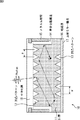
図1は、本開示の実施の形態である裏面照射型の固体撮像素子10の構成例を示す断面図である。
<Configuration example of solid-state image sensor>
FIG. 1 is a cross-sectional view illustrating a configuration example of a backside illumination type solid-
ただし、図面の上側が受光面(裏面)であり、受光面のさらに上側に配置されるべきカラーフィルタ、オンチップレンズ等は図示を省略している。また、同図においては、1画素分の構成例を示しているが、該裏面照射型の固体撮像素子10から成る2次元固体撮像素子は、X×Y(X,Yは整数)個の隣接する画素が1チップ上に形成されており、さらにN×M(N<X,M<Y。例えば、2×2)個の隣接する画素によって1ユニットを構成し、1ユニットの各画素がR,G,B,IRのいずれかの波長の光(電磁波)を検出するようになされている。以降の図面においても同様とする。
However, the upper side of the drawing is the light receiving surface (back surface), and the color filter, the on-chip lens, and the like that are to be arranged further above the light receiving surface are not shown. In addition, in the same figure, a configuration example for one pixel is shown. However, the two-dimensional solid-state image pickup device including the back-illuminated solid-state
図1の構成例において、光吸収層であるSi層11には、その受光面(図面上側の面)に周期的(周期P)であって微細な凹凸パターン12が形成されている。また、受光面の反対側(図中下側)の面にも同様に、周期的(周期P’)であって微細な凹凸パターン13が形成されている。凹凸パターン12は、可視波長全域から赤外波長域までの広帯域の光に対する、反射率が低い良質な反射防止膜として作用することができる。また、周期的な構造とすることにより、Siの表面積の増加を有限に留めることができる。これにより、半導体結晶の結晶欠陥起因の暗電流、ランダムノイズ、白点の増加などを抑制することができる。なお、凹凸パターン12,13の形状、サイズなどについては後述する。
In the configuration example of FIG. 1, the
また、図1の構成例において、隣接する画素との境、すなわち、Si層11の図中横側には、Siに対して相対的に低い屈折率を有する誘電体(SiO2など)で充填された素子分離構造14が形成されている。なお、図1の場合、素子分離構造14の形状は、角柱であり、受光面側からのエッチングにより形成されている。さらに、素子分離構造14の内部には、メタル反射壁15が配置されている。
In the configuration example of FIG. 1, the boundary between adjacent pixels, that is, the lateral side of the
Si層11の下層側には、絶縁膜16を介して、Al,Cu,Ag、またはそれらの合金からなる反射ミラー構造17が形成されている。なお、反射ミラー構造17は、入射光の反射を目的として専用の膜や層を形成する代わりに、Si層11の下層側に設けられる各種の配線層に反射ミラー構造17としての機能を兼ねさせてもよい。凹凸パターン12が形成されたSi層11の上層側には、SiO2,SiNなどからなる平坦化膜18が形成されている。
A
上述したように、図1に示される構成例の場合、Si層11の受光面とその反対面のそれぞれに凹凸パターン12,13が形成されている。さらに、隣接する画素との境には素子分離構造14が、Si層11の下層側には反射ミラー構造17が形成されている。これにより、入射光がSi層11の内部で反射を繰り返し易くなり、光のSi層11からの透過が抑止されるので、Si層11における光吸収効率を向上させることができる。すなわち、入射光に対する感度を上げることができる。また、素子分離構造14およびメタル反射壁15により、隣接する画素に起因する混色が抑止される。
As described above, in the configuration example shown in FIG. 1, the
<固体撮像素子の変形例1>
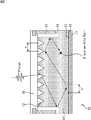
図2は、本開示の実施の形態である固体撮像素子10の他の構成例(変形例1)を示す断面図である。ただし、図1に示された構成例と共通する構成要素については、同一の符号を付しているので、その説明は適宜省略する。
<Modification Example 1 of Solid-State Image Sensor>
FIG. 2 is a cross-sectional view illustrating another configuration example (modification example 1) of the solid-
図2に示される変形例1は、Si層11の下層側の面に形成されている凹凸パターン13の周期が無限に小さいものに変更されている。
In
変形例1の場合、Si層11の受光面とその反対面のそれぞれに凹凸パターン12,13が形成されている。さらに、隣接する画素との境には素子分離構造14が、Si層11の下層側には反射ミラー構造17が形成されている。これにより、入射光がSi層11の内部で反射を繰り返し易くなり、光のSi層11からの透過が抑止されるので、Si層11における光吸収効率を向上させることができる。すなわち、入射光に対する感度を上げることができる。また、素子分離構造14およびメタル反射壁15により、隣接する画素に起因する混色が抑止される。
In the case of the
<固体撮像素子の変形例2>
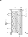
図3は、本開示の実施の形態である固体撮像素子10のさらに他の構成例(変形例2)を示す断面図である。ただし、図1に示された構成例と共通する構成要素については、同一する符号を付しているので、その説明は適宜省略する。
<Modification Example 2 of Solid-State Image Sensor>
FIG. 3 is a cross-sectional view showing still another configuration example (modification example 2) of the solid-
図3に示される変形例2は、図1に示された構成例から、メタル反射壁15が省略されている。
In the second modification shown in FIG. 3, the
変形例2の場合、Si層11の受光面面とその反対面のそれぞれに凹凸パターン12,13が形成されている。さらに、隣接する画素との境には素子分離構造14が、Si層11の下層側には反射ミラー構造17が形成されている。これにより、入射光がSi層11の内部で反射を繰り返し易くなり、光のSi層11からの透過が抑止されるので、Si層11における光吸収効率を向上させることができる。すなわち、入射光に対する感度を上げることができる。
In the case of the modification 2, the uneven |
<固体撮像素子の変形例3>
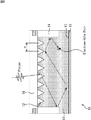
図4は、本開示の実施の形態である固体撮像素子10のさらに他の構成例(変形例3)を示す断面図である。ただし、図1に示された構成例と共通する構成要素については、同一の符号を付しているので、その説明は適宜省略する。
<Modification 3 of the solid-state imaging device>
FIG. 4 is a cross-sectional view illustrating still another configuration example (modification example 3) of the solid-
図4に示される変形例3は、図1に示された構成例から、メタル反射壁15、および反射ミラー構造17が省略されている。
In the third modification shown in FIG. 4, the
変形例3の場合、Si層11の受光面とその反対面のそれぞれに凹凸パターン12,13が形成されている。さらに、隣接する画素との境には素子分離構造14が設けられている。これにより、入射光がSi層11の内部で反射を繰り返し易くなり、光のSi層11からの透過が抑止されるので、Si層11における光吸収効率を向上させることができる。すなわち、入射光に対する感度を上げることができる。
In the case of the modification 3, the uneven |
<固体撮像素子の変形例4>
図5は、本開示の実施の形態である固体撮像素子10のさらに他の構成例(変形例4)を示す断面図である。ただし、図1に示された構成例と共通する構成要素については、同一の符号を付しているので、その説明は適宜省略する。
<Modification Example 4 of Solid-State Image Sensor>
FIG. 5 is a cross-sectional view illustrating still another configuration example (modification example 4) of the solid-
図5に示される変形例4は、図1に示された構成例における凹凸パターン13の周期が無限に小さいものに変更され、かつ、メタル反射壁15が省略されている。
In Modification 4 shown in FIG. 5, the period of the concavo-
変形例4の場合、Si層11の受光面とその反対面のそれぞれに凹凸パターン12,13が形成されている。さらに、隣接する画素との境には素子分離構造14が設けられている。これにより、入射光がSi層11の内部で反射を繰り返し易くなり、光のSi層11からの透過が抑止されるので、Si層11における光吸収効率を向上させることができる。すなわち、入射光に対する感度を上げることができる。
In the case of the modification 4, the uneven |
<固体撮像素子の変形例5>
図6は、本開示の実施の形態である固体撮像素子10のさらに他の構成例(変形例5)を示す断面図である。ただし、図1に示された構成例と共通する構成要素については、同一の符号を付しているので、その説明は適宜省略する。
<Modification 5 of the solid-state imaging device>
FIG. 6 is a cross-sectional view illustrating still another configuration example (modification example 5) of the solid-
図6に示される変形例5は、図1に示された構成例における凹凸パターン13の周期が無限に小さいものに変更され、かつ、メタル反射壁15および反射ミラー構造17が省略されている。
In Modification 5 shown in FIG. 6, the period of the
変形例5の場合、Si層11の受光面とその反対面のそれぞれに凹凸パターン12,13が形成されている。さらに、隣接する画素との境には素子分離構造14が設けられている。これにより、入射光がSi層11の内部で反射を繰り返し易くなり、光のSi層11からの透過が抑止されるので、Si層11における光吸収効率を向上させることができる。すなわち、入射光に対する感度を上げることができる。
In the case of the modification 5, the uneven |
<固体撮像素子の変形例6>
図7は、本開示の実施の形態である固体撮像素子10のさらに他の構成例(変形例6)を示す断面図である。ただし、図1に示された構成例と共通する構成要素については、同一の符号を付しているので、その説明は適宜省略する。
<Modification 6 of the solid-state imaging device>
FIG. 7 is a cross-sectional view showing still another configuration example (modification example 6) of the solid-
図7に示される変形例6は、図1に示された構成例における凹凸パターン13の周期が無限に小さいものに変更され、かつ、メタル反射壁15が省略されている。さらに、素子分離構造14の形状が変更されている。具体的には、素子分離構造14の形状が、受光面側からその反対側に向かって徐々に狭められたくさび型に変更されている。素子分離構造14の形状をくさび型とすることにより、図1の構成例などのように、素子分離構造14の形状が角柱である場合に比較して、Si層11における横方向の反射光率をより高めることができる。
In Modification 6 shown in FIG. 7, the period of the concavo-
変形例6の場合、Si層11の受光面とその反対面のそれぞれに凹凸パターン12,13が形成されている。さらに、離接する画素との境にはくさび型の素子分離構造14が設けられている。これにより、入射光がSi層11の内部で反射を繰り返し易くなり、光のSi層11からの透過が抑止されるので、Si層11における光吸収効率を向上させることができる。すなわち、入射光に対する感度を上げることができる。
In the case of the modification 6, the uneven |
<固体撮像素子の変形例7>
図8は、本開示の実施の形態である固体撮像素子10のさらに他の構成例(変形例7)を示す断面図である。ただし、図1に示された構成例と共通する構成要素については、同一の符号を付しているので、その説明は適宜省略する。
<Modification Example 7 of Solid-State Image Sensor>
FIG. 8 is a cross-sectional view illustrating still another configuration example (modification example 7) of the solid-
図8に示される変形例7は、図1に示された構成例における凹凸パターン13の周期が無限に小さいものに変更され、かつ、メタル反射壁15が省略されている。さらに、素子分離構造14の形状が、受光面の反対側から受光面側に向かって徐々に狭められたくさび型に変更されている。素子分離構造14をくさび型とすることにより、図1の構成例などのように、素子分離構造14の形状が角柱である場合に比較して、Si層11における横方向の反射光率をより高めることができる。
In the modified example 7 shown in FIG. 8, the period of the
変形例7の場合、Si層11の受光面とその反対面のそれぞれに凹凸パターン12,13が形成されている。さらに、隣接する画素との境にはくさび型の素子分離構造14が設けられている。これにより、入射光がSi層11の内部で反射を繰り返し易くなり、光のSi層11からの透過が抑止されるので、Si層11における光吸収効率を向上させることができる。すなわち、入射光に対する感度を上げることができる。
In the case of the modification 7, the uneven |
<固体撮像素子の変形例8>
図9は、本開示の実施の形態である固体撮像素子10のさらに他の構成例(変形例8)を示す断面図である。ただし、図1に示された構成例と共通する構成要素については、同一の符号を付しているので、その説明は適宜省略する。
<Modified Example 8 of Solid-State Image Sensor>
FIG. 9 is a cross-sectional view illustrating still another configuration example (modified example 8) of the solid-
図9に示される変形例8は、図1に示された構成例に対して、Si層11に形成されている凹凸パターン12の上層側に、凹凸パターン12の形状を反転した形状の、入射側から見て段階的に屈折率が変化するモスアイ構造21が追加されている。
Modification 8 shown in FIG. 9 is incident on the upper side of the concavo-
変形例8の場合、Si層11の受光面にモスアイ構造21および凹凸パターン12が、その反対面に凹凸パターン13が形成されている。さらに、隣接する画素との境には素子分離構造14が、Si層11の下層側には反射ミラー構造17が形成されている。これにより、入射光がSi層11の内部で反射を繰り返し易くなり、光のSi層11からの透過が抑止されるので、Si層11における光吸収効率を向上させることができる。すなわち、入射光に対する感度を上げることができる。また、素子分離構造14およびメタル反射壁15により、隣接する画素に起因する混色が抑止される。
In the case of the modification 8, the moth-eye structure 21 and the concavo-
<固体撮像素子の変形例9>
図10は、本開示の実施の形態である固体撮像素子10のさらに他の構成例(変形例9)を示す断面図である。ただし、図1に示された構成例と共通する構成要素については、同一の符号を付しているので、その説明は適宜省略する。
<Modified Example 9 of Solid-State Image Sensor>
FIG. 10 is a cross-sectional view illustrating still another configuration example (modification 9) of the solid-
図10に示される変形例9は、図1に示された構成例に対して、Si層11に形成されている凹凸パターン12の上層側に、平坦化膜18とSi層11の中間的な屈折率を有する中間膜31が設けられている。中間膜31の素材には、ハフニウム酸化膜、アルミニウム酸化物、またはシリコン窒化膜などが用いられる。なお、中間膜31は、凹部の深さに比べて十分に薄く、凹凸パターン12と相似的な形状を取ることが好ましい。さらに、中間膜31の上層側にはカラーフィルタ32が追加されている。
The modification 9 shown in FIG. 10 is an intermediate between the
変形例9の場合、Si層11の受光面とその反対面のそれぞれに凹凸パターン12,13が形成されている。さらに、隣接する画素との境には素子分離構造14が、Si層11の下層側には反射ミラー構造17が形成されている。これにより、入射光がSi層11の内部で反射を繰り返し易くなり、光のSi層11からの透過が抑止されるので、Si層11における光吸収効率を向上させることができる。すなわち、入射光に対する感度を上げることができる。また、素子分離構造14およびメタル反射壁15により、隣接する画素に起因する混色が抑止される。さらに、カラーフィルタが一体的に形成されるので、カラーフィルタを別途配置する場合に比較して、固体撮像素子10の厚みを削減することができる。
In the case of the modification 9, the uneven |
なお、上述した固体撮像素子10の構成例とその変形例2乃至9は、適宜組み合わせることができる。
Note that the above-described configuration example of the solid-
<凹凸パターン12,13の構造例>
次に、Si層11の受光面とその反対面のそれぞれに形成される凹凸パターン12,13の構造について説明する。
<Structural example of
Next, the structure of the concavo-
図11は、凹凸パターン12,13の構造として、逆ピラミッド型、順ピラミッド型、Vグルーブ型、およびXグルーブ型の4例を挙げ、その上面図および断面図を示している。
FIG. 11 shows four examples of the structures of the concave and
逆ピラミッド型は、Si層11の面(受光面とその反対面)に対して四角錐形状の凹構造が周期的に形成されたものである。順ピラミッド型は、Si層11の面に対して四角錐形状の凸構造が周期的に形成されたものである。
In the inverted pyramid type, a concave structure having a quadrangular pyramid shape is periodically formed on the surface of the Si layer 11 (light receiving surface and its opposite surface). In the forward pyramid type, a convex structure having a quadrangular pyramid shape is periodically formed on the surface of the
Vグルーブ型は、Si層11の面に対して平行に並んだ直線状の溝構造が周期的に形成されたものである。Xグルーブ型は、Si層11の面に対して平行に並んだ直線状の第1溝構造と、第1溝構造に直交する方向に平行に並んだ直線状の第2溝構造とが周期的に形成されたものである。
In the V-groove type, a linear groove structure arranged in parallel with the surface of the
なお、凹凸パターン12の構造と凹凸パターン13の構造とは同一の型であってもよいし、異なる型であってもよい。また、凹凸パターン12,13の構造は、上述した4例の型に限るものではなく、周期的に同一の構造を形成するようにすればよい。
The structure of the
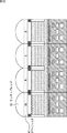
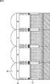
<凹凸パターン12,13が採用される画素の例>
上述したように、本実施の形態である固体撮像素子10は、N×M(N<X,M<Y。例えば、2×2)個の隣接する画素で1ユニットを構成し、1ユニットの各画素がR,G,B,IRのいずれかの波長の光を検出するようになされている。
<Example of pixels in which
As described above, in the solid-
図12は、本実施の形態である固体撮像素子10における1ユニット分の画素の断面図を示している。同図の場合、R,G,B,IRそれぞれの波長の光を検出する各画素のうち、光吸収効率が相対的に低い最長波長側のIRを検出する画素に対してのみ、凹凸パターン12,13が採用されている。ただし、同図において、凹凸パターン13の図示は省略されている。
FIG. 12 shows a cross-sectional view of one unit of pixels in the solid-
図13は、本実施の形態である固体撮像素子10における1ユニット分の画素の断面図を示している。同図の場合、R,G,B,IRそれぞれの波長の光を検出する各画素のうち、光吸収効率が相対的に低い長波長側のIRとRをそれぞれ検出する画素に対してのみ、凹凸パターン12,13が採用されている。ただし、同図において、凹凸パターン13の図示は省略されている。
FIG. 13 shows a cross-sectional view of one unit of pixels in the solid-
図14は、本実施の形態である固体撮像素子10における1ユニット分の画素の断面図を示している。同図の場合、R,G,B,IRそれぞれの波長の光を検出する全ての画素に凹凸パターン12,13が採用されている。ただし、同図において、凹凸パターン13の図示は省略されている。
FIG. 14 shows a cross-sectional view of one unit of pixels in the solid-
図15は、本実施の形態である固体撮像素子10における1ユニット分の画素の断面図を示している。同図の場合、R,G,B,IRそれぞれの波長の光を検出する全ての画素に凹凸パターン12,13が採用され、検出する波長に応じて凹凸パターン12,13のサイズ(周期)が異なる場合を示している。すなわち、光吸収効率が相対的に低い長波長側から、相対的に高い短波長側に向かって、凹凸パターン12,13の周期が短くなるように形成されている。つまり、IR用の画素の凹凸パターン12,13の周期が最も長く、B用の画素の凹凸パターン12,13の周期が最も短い。ただし、同図において、凹凸パターン13の図示は省略されている。
FIG. 15 shows a cross-sectional view of one unit of pixels in the solid-
次に、図16は、本実施の形態である固体撮像素子10を、光の入射面側に各種の画素配線等が設けられている表面照射型の固体撮像素子に適用した場合における1ユニット分の画素の断面図を示している。同図の場合、R,G,B,IRそれぞれの波長の光を検出する全ての画素に凹凸パターン12,13が採用されている。ただし、同図において、凹凸パターン13の図示は省略されている。同図に示す表面照射型の固体撮像素子10において、光吸収層の裏面側にミラー構造を配置する場合、配線などが裏面側にないので、ミラー構造を画素間に隙間なく配置することができる。
Next, FIG. 16 shows one unit when the solid-
図12乃至図16に示されたように、凹凸パターン12,13は、必ずしも、R,G,B,IRの各画素のすべてに凹凸パターン12,13が形成されていなくてもよいが、少なくともIRの画素には、凹凸パターン12,13が形成されているようにする。
As shown in FIG. 12 to FIG. 16, the concave /
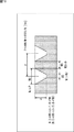
<光吸収効率のシミュレーション>
次に、本実施の形態である固体撮像素子10のSi層11における光吸収効率について説明する。
<Simulation of light absorption efficiency>
Next, the light absorption efficiency in the
図17は、入射光の波長に対するSi層の光吸収効率の変化をミュレーションした結果を示している。ただし、同図において、横軸は入射光の波長を示し、縦軸はSi層における光吸収効率を示している。また、Si層については、その厚さを3umと仮定している。 FIG. 17 shows the result of simulating the change in light absorption efficiency of the Si layer with respect to the wavelength of incident light. In this figure, the horizontal axis indicates the wavelength of incident light, and the vertical axis indicates the light absorption efficiency in the Si layer. The thickness of the Si layer is assumed to be 3 μm.
同図において、曲線aは、Si層の面(受光面とその反対面)に凹凸パターンが形成されていない従来の固体撮像素子の特性に対するシミュレーション結果を示している。曲線bは、Si層の両面に凹凸パターンが形成されておらず、Si層の下層側に反射ミラー構造を有する固体撮像素子の特性に対するシミュレーション結果を示している。曲線c,dは、本実施の形態である固体撮像素子10、すなわち、Si層11の両面に凹凸パターン12,13が形成されており、反射ミラー構造17を有する固体撮像素子の特性に対するシミュレーション結果を示している。
In the figure, a curve a shows a simulation result with respect to characteristics of a conventional solid-state imaging device in which a concavo-convex pattern is not formed on the surface of the Si layer (the light receiving surface and the opposite surface). A curve b shows a simulation result with respect to the characteristics of the solid-state imaging device in which the uneven pattern is not formed on both surfaces of the Si layer and the reflection mirror structure is provided on the lower layer side of the Si layer. Curves c and d are simulation results for the characteristics of the solid-
曲線aが示す特性は、全ての波長帯域において、他の曲線よりも光吸収効率が低く、特にその傾向が長波長側で顕著である。曲線bが示す特性は、波長650nm〜900nmの範囲において、曲線aよりも10%から20%程度の光吸収効率の改善が見られる。曲線c,dでは、全ての波長帯域において、曲線a,bの特性よりも光吸収効率の改善が見られ、特に、赤色光から赤外線に相当する波長700nm〜900nmの範囲において顕著な光吸収効率の改善が見られる。したがって、本実施の形態である固体撮像素子10は、R,G,B,IRの各波長をそれぞれ検知する場合においてSi層11の光吸収効率を改善する効果を有し、特に、相対的に長波長側のR,IRをそれぞれ検知する場合において、Si層11の光吸収効率大きく改善する効果を有するといえる。
The characteristic indicated by the curve a has lower light absorption efficiency than other curves in all wavelength bands, and the tendency is particularly remarkable on the long wavelength side. The characteristic shown by the curve b shows an improvement in light absorption efficiency of about 10% to 20% over the curve a in the wavelength range of 650 nm to 900 nm. In the curves c and d, the light absorption efficiency is improved in all wavelength bands as compared with the characteristics of the curves a and b. In particular, the light absorption efficiency is remarkable in the wavelength range of 700 nm to 900 nm corresponding to infrared rays. The improvement is seen. Therefore, the solid-
<凹凸パターン12のサイズ制約>
次に、凹凸パターン12のサイズ制約について説明する。図18は、凹凸パターン12のサイズと周期Pの関係を示している。
<Restriction of
Next, the size restriction of the
凹凸パターン12の周期Pは、400/N乃至1500/N[nm]を好適とする。Nは、凹凸パターン12の周囲の媒質の屈折率である。N=1.5である場合、周期Pは1000nm=1um以下となる。凹凸パターン12の開口上部の幅W1は、周期P以下とする。凹凸パターン12の開口底部の幅W2は、凹凸パターン12の開口上部の幅W1よりも狭いものとする。凹凸パターン12の隣接する凹部の間隔W3は、0以上とする。凹凸パターン12の深さdは、開口上部の幅W1よりも狭いものとする。具体的には、0.3・W1<d<1.0・W1または0.5・W1<d<0.8・W1とする。
The period P of the concavo-
なお、凹凸パターン13のサイズについても同様に制約があるものとする。
It is assumed that the size of the
<凹凸パターン12,13の形成工程>
次に、凹凸パターン12,13の形成工程について説明する。図19は、凹凸パターン12,13の形成工程の一例を示している。
<Formation process of
Next, the formation process of the
まず同図Aに示されるように、Si層11の表面にレジストを塗布し、次に同図Bに示されるように、凹凸パターンの凹部を形成する箇所にEUV露光や電子ビーム描画などで露光することによりマーキングを行う。
First, as shown in FIG. 1A, a resist is applied to the surface of the
次に同図Cに示されるように、塗布されているレジストのマーキング箇所を除去し、同図Dに示されるように、ウェットエッチング、またはドライエッチングにより結晶性の異方性エッチングを行って凹部を形成し、同図Eに示されるように、レジストを除去する。 Next, as shown in Fig. C, the marking portion of the applied resist is removed, and as shown in Fig. D, a crystalline anisotropic etching is performed by wet etching or dry etching to form a recess. And the resist is removed as shown in FIG.
さらに、同図Fに示されるように、異方性エッチングを行った凹部を含むSi層11の表面に、平坦化膜18とSi層11との中間的な屈折率を有する中間膜31を成膜する。中間膜31の素材には、ハフニウム酸化膜、アルミニウム酸化物、またはシリコン窒化膜などの高誘電体を用いればよい。なお、中間膜31は、凹部の深さに比べて十分に薄く、凹凸パターンと相似的な形状を取ることが好ましい。最後に、同図Gに示されるように、中間膜31の上層に、誘電体からなる平坦化膜18を成膜する。平坦化膜の素材には、SiO2,SiNなどを採用する。
Further, as shown in FIG. 5F, an
なお、凹凸パターンの凹部を形成するに際しては、同図Hおよび同図Iに示されるように、Si層11の受光面およびその反対面を結晶面(100)面とし、凹部の壁面を結晶面(111)面とすれば、結晶性の異方性エッチングにより、結晶欠陥を抑止しつつ高精度な凹凸パターンを形成することができる。
When forming the concave portion of the concave-convex pattern, as shown in FIG. H and FIG. I, the light receiving surface of the
<まとめ>
以上に説明した本実施の形態である固体撮像素子10によれば、Si層11の厚みを増すことなく、R,G,B,IRの各波長帯域での受光感度を向上させることができ、特に、IR波長帯域での受光感度を大きく向上させることができる。
<Summary>
According to the solid-
なお、本開示の実施の形態である固体撮像素子10は、裏面照射型、または表面照射型のどちらにも適用可能である。
Note that the solid-
また、本実施の形態である固体撮像素子10は、デジタルビデオカメラやデジタルスチルカメラに代表される撮像装置を含む、固体撮像素子を用いた撮像機能やセンシング機能を有するあらゆる種類の電子装置に適用することができる。
Further, the solid-
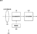
<電子装置の構成例>
図20は、本実施の形態である固体撮像素子10を適用した電子装置の構成例を示している。
<Configuration example of electronic device>
FIG. 20 shows a configuration example of an electronic apparatus to which the solid-
この電子装置100は、上述した固体撮像素子10を用いた撮像機能を有するものである。電子装置100は、固体撮像素子10、光学系構成部101、駆動部102、および信号処理部103を備える。
The
光学系構成部101は、光学レンズなどから構成され、被写体の光学像を固体撮像素子10に入射させる。駆動部102は、固体撮像素子10の内部の駆動に関する各種のタイミング信号を生成、出力することにより固体撮像素子10の駆動を制御する。信号処理部103は、固体撮像素子10から出力される画像信号に対して所定の信号処理を施し、その信号処理結果に応じた処理を実行する。また、信号処理部103は、信号処理結果の画像信号を後段に出力して、例えば、固体メモリなどの記録媒体に記録したり、所定のネットワークを介し、所定のサーバに転送したりする。
The optical
本開示の実施の形態は、上述した実施の形態に限定されるものではなく、本開示の要旨を逸脱しない範囲において種々の変更が可能である。 Embodiments of the present disclosure are not limited to the above-described embodiments, and various modifications can be made without departing from the scope of the present disclosure.
なお、本開示は以下のような構成も取ることができる。
(1)
多数の画素が縦横に配置されている固体撮像素子において、
光検出素子としての光吸収層の受光面とその反対面に周期的な凹凸パターンを
備える固体撮像素子。
(2)
前記光吸収層は、単結晶Siからなる
前記(1)に記載の固体撮像素子。
(3)
前記多数の画素のうち、少なくともIR検出用の画素に対応する前記光吸収層の受光面とその反対面には前記凹凸パターンが形成されている
前記(1)または(2)に記載の固体撮像素子。
(4)
前記光吸収層の受光面の反対面に形成されている前記凹凸パターンの周期は無限に小さい
前記(1)から(3)のいずれかに記載の固体撮像素子。
(5)
前記光吸収層の受光面とその反対面に形成されている前記凹凸パターンの周期は、検知する波長に応じて異なる
前記(1)から(4)のいずれかに記載の固体撮像素子。
(6)
前記凹凸パターンは、1次元周期的、または2次元周期的に形成されている
前記(1)から(5)のいずれかに記載の固体撮像素子。
(7)
前記凹凸パターンが形成される前記光吸収層の前記受光面および前記反対面の結晶面は、(100)面であり、前記凹凸パターンの壁面の結晶面は、(111)面である
前記(1)から(6)のいずれかに記載の固体撮像素子。
(8)
前記凹凸パターンの周期は、1um以下である
前記(1)から(7)のいずれかに記載の固体撮像素子。
(9)
前記光吸収層の隣接する画素との境には、素子分離構造が形成されている
前記(1)から(8)のいずれかに記載の固体撮像素子。
(10)
前記素子分離構造には、前記光吸収層よりも屈折率が低い素材からなる
前記(9)に記載の固体撮像素子。
(11)
前記素子分離構造の内部には、メタル反射壁が形成されている
前記(9)または(10)に記載の固体撮像素子。
(12)
前記光吸収層の下層側に反射ミラー構造を
さらに備える前記(1)から(11)のいずれかに記載の固体撮像素子。
(13)
前記反射ミラー構造は、配線層が兼ねる
前記(12)に記載の固体撮像素子。
(14)
多数の画素が縦横に配置されている固体撮像素子を搭載する電子装置において、
前記固体撮像素子は、
光検出素子としての光吸収層の受光面とその反対面に周期的な凹凸パターンを備える
電子装置。
In addition, this indication can also take the following structures.
(1)
In a solid-state imaging device in which a large number of pixels are arranged vertically and horizontally,
A solid-state imaging device comprising a light-receiving surface of a light absorption layer as a light detection device and a periodic uneven pattern on the opposite surface.
(2)
The solid-state imaging device according to (1), wherein the light absorption layer is made of single crystal Si.
(3)
The solid-state imaging according to (1) or (2), wherein the uneven pattern is formed on a light receiving surface of the light absorption layer corresponding to at least an IR detection pixel and the opposite surface among the plurality of pixels. element.
(4)
The solid-state imaging device according to any one of (1) to (3), wherein a period of the concavo-convex pattern formed on a surface opposite to the light receiving surface of the light absorption layer is infinitely small.
(5)
The solid-state imaging device according to any one of (1) to (4), wherein a period of the concavo-convex pattern formed on the light receiving surface of the light absorption layer and the opposite surface thereof varies depending on a wavelength to be detected.
(6)
The solid-state imaging device according to any one of (1) to (5), wherein the uneven pattern is formed in a one-dimensional periodic manner or a two-dimensional periodic manner.
(7)
The light-receiving surface and the opposite crystal plane of the light absorption layer on which the concave / convex pattern is formed are (100) planes, and the crystal plane of the concave / convex pattern is (111) planes (1) ) To (6).
(8)
The period of the concavo-convex pattern is 1 μm or less. The solid-state imaging device according to any one of (1) to (7).
(9)
The solid-state imaging device according to any one of (1) to (8), wherein an element isolation structure is formed at a boundary between adjacent pixels of the light absorption layer.
(10)
The solid-state imaging device according to (9), wherein the element isolation structure is made of a material having a refractive index lower than that of the light absorption layer.
(11)
The solid-state image sensor according to (9) or (10), wherein a metal reflection wall is formed inside the element isolation structure.
(12)
The solid-state imaging device according to any one of (1) to (11), further including a reflection mirror structure on a lower layer side of the light absorption layer.
(13)
The solid-state imaging device according to (12), wherein the reflection mirror structure also serves as a wiring layer.
(14)
In an electronic device equipped with a solid-state imaging device in which a large number of pixels are arranged vertically and horizontally,
The solid-state imaging device is
An electronic apparatus comprising a light-receiving surface of a light absorption layer as a light detection element and a periodic uneven pattern on the opposite surface.
10 固体撮像素子, 11 Si層, 12,13 凹凸パターン, 14 素子分離構造, 15 メタル反射壁, 16 絶縁膜, 17 反射ミラー構造, 18 平坦化膜, 31 中間膜, 32 カラーフィルタ
DESCRIPTION OF
Claims (14)
光検出素子としての光吸収層の受光面とその反対面に周期的な凹凸パターンを
備える固体撮像素子。 In a solid-state imaging device in which a large number of pixels are arranged vertically and horizontally,
A solid-state imaging device comprising a light-receiving surface of a light absorption layer as a light detection device and a periodic uneven pattern on the opposite surface.
請求項1に記載の固体撮像素子。 The solid-state imaging device according to claim 1, wherein the light absorption layer is made of single crystal Si.
請求項2に記載の固体撮像素子。 3. The solid-state imaging device according to claim 2, wherein the uneven pattern is formed on a light receiving surface of the light absorption layer corresponding to at least an IR detection pixel and the opposite surface among the plurality of pixels.
請求項2に記載の固体撮像素子。 The solid-state imaging device according to claim 2, wherein a period of the concavo-convex pattern formed on a surface opposite to the light receiving surface of the light absorption layer is infinitely small.
請求項2に記載の固体撮像素子。 The solid-state imaging device according to claim 2, wherein a period of the concave / convex pattern formed on the light receiving surface of the light absorption layer and the opposite surface thereof varies depending on a wavelength to be detected.
請求項2に記載の固体撮像素子。 The solid-state imaging device according to claim 2, wherein the uneven pattern is formed in a one-dimensional periodic manner or a two-dimensional periodic manner.
請求項2に記載の固体撮像素子。 The crystal plane of the light receiving surface and the opposite surface of the light absorption layer on which the concave / convex pattern is formed is a (100) plane, and the crystal plane of the wall surface of the concave / convex pattern is a (111) plane. The solid-state image sensor described in 1.
請求項2に記載の固体撮像素子。 The solid-state imaging device according to claim 2, wherein a period of the uneven pattern is 1 μm or less.
請求項2に記載の固体撮像素子。 The solid-state imaging device according to claim 2, wherein an element isolation structure is formed at a boundary between adjacent pixels of the light absorption layer.
請求項9に記載の固体撮像素子。 The solid-state imaging device according to claim 9, wherein the element isolation structure is made of a material having a refractive index lower than that of the light absorption layer.
請求項9に記載の固体撮像素子。 The solid-state imaging device according to claim 9, wherein a metal reflection wall is formed inside the element isolation structure.
さらに備える請求項2に記載の固体撮像素子。 The solid-state imaging device according to claim 2, further comprising a reflection mirror structure on a lower layer side of the light absorption layer.
請求項12に記載の固体撮像素子。 The solid-state imaging device according to claim 12, wherein the reflection mirror structure also serves as a wiring layer.
前記固体撮像素子は、
光検出素子としての光吸収層の受光面とその反対面に周期的な凹凸パターンを備える
電子装置。 In an electronic device equipped with a solid-state imaging device in which a large number of pixels are arranged vertically and horizontally,
The solid-state imaging device is
An electronic apparatus comprising a light-receiving surface of a light absorption layer as a light detection element and a periodic uneven pattern on the opposite surface.
Priority Applications (8)
| Application Number | Priority Date | Filing Date | Title |
|---|---|---|---|
| JP2014120205A JP2016001633A (en) | 2014-06-11 | 2014-06-11 | Solid state image sensor and electronic equipment |
| CN201580029430.9A CN106463518B (en) | 2014-06-11 | 2015-05-29 | Solid-state imaging element and electronic device |
| CN201811252560.0A CN109638028B (en) | 2014-06-11 | 2015-05-29 | Solid-state imaging element and electronic device |
| PCT/JP2015/065534 WO2015190318A1 (en) | 2014-06-11 | 2015-05-29 | Solid-state imaging element and electronic device |
| US15/312,069 US10411053B2 (en) | 2014-06-11 | 2015-05-29 | Solid state imaging element and electronic device to obtain high sensitivity of light on a long wavelength side |
| US16/563,582 US11329080B2 (en) | 2014-06-11 | 2019-09-06 | Solid state imaging element and electronic device |
| US16/797,922 US11081508B2 (en) | 2014-06-11 | 2020-02-21 | Solid state imaging element and electronic device |
| US17/719,863 US20220238567A1 (en) | 2014-06-11 | 2022-04-13 | Solid state imaging element and electronic device |
Applications Claiming Priority (1)
| Application Number | Priority Date | Filing Date | Title |
|---|---|---|---|
| JP2014120205A JP2016001633A (en) | 2014-06-11 | 2014-06-11 | Solid state image sensor and electronic equipment |
Related Child Applications (1)
| Application Number | Title | Priority Date | Filing Date |
|---|---|---|---|
| JP2017253205A Division JP2018088532A (en) | 2017-12-28 | 2017-12-28 | Solid-state imaging element and electronic device |
Publications (2)
| Publication Number | Publication Date |
|---|---|
| JP2016001633A true JP2016001633A (en) | 2016-01-07 |
| JP2016001633A5 JP2016001633A5 (en) | 2017-02-23 |
Family
ID=54833419
Family Applications (1)
| Application Number | Title | Priority Date | Filing Date |
|---|---|---|---|
| JP2014120205A Pending JP2016001633A (en) | 2014-06-11 | 2014-06-11 | Solid state image sensor and electronic equipment |
Country Status (4)
| Country | Link |
|---|---|
| US (4) | US10411053B2 (en) |
| JP (1) | JP2016001633A (en) |
| CN (2) | CN109638028B (en) |
| WO (1) | WO2015190318A1 (en) |
Cited By (27)
| Publication number | Priority date | Publication date | Assignee | Title |
|---|---|---|---|---|
| WO2018061898A1 (en) * | 2016-09-27 | 2018-04-05 | 日本電気株式会社 | Optical sensor and method for forming same |
| JP2018088532A (en) * | 2017-12-28 | 2018-06-07 | ソニー株式会社 | Solid-state imaging element and electronic device |
| KR20180060969A (en) * | 2016-11-29 | 2018-06-07 | 타이완 세미콘덕터 매뉴팩쳐링 컴퍼니 리미티드 | Qe approach by double-side, multi absorption structure |
| CN108376689A (en) * | 2017-02-01 | 2018-08-07 | 三星电子株式会社 | Imaging sensor and the method for manufacturing it |
| US10050078B2 (en) | 2016-12-28 | 2018-08-14 | Samsung Electronics Co., Ltd. | Light sensor |
| JP2018525837A (en) * | 2015-08-21 | 2018-09-06 | クアルコム,インコーポレイテッド | System and method for extending near infrared spectral response for imaging systems |
| KR20190037074A (en) * | 2017-09-28 | 2019-04-05 | 타이완 세미콘덕터 매뉴팩쳐링 컴퍼니 리미티드 | Image sensor with improved quantum efficiency surface structure |
| US10411053B2 (en) | 2014-06-11 | 2019-09-10 | Sony Corporation | Solid state imaging element and electronic device to obtain high sensitivity of light on a long wavelength side |
| WO2020012984A1 (en) * | 2018-07-13 | 2020-01-16 | ソニーセミコンダクタソリューションズ株式会社 | Sensor device and electronic apparatus |
| JP2020027937A (en) * | 2018-08-10 | 2020-02-20 | ブリルニクス インク | Solid-state imaging device, manufacturing method thereof, and electronic apparatus |
| WO2020209126A1 (en) * | 2019-04-12 | 2020-10-15 | ソニーセミコンダクタソリューションズ株式会社 | Solid-state imaging device |
| WO2020209107A1 (en) * | 2019-04-12 | 2020-10-15 | ソニーセミコンダクタソリューションズ株式会社 | Solid-state imaging device |
| WO2021005961A1 (en) * | 2019-07-11 | 2021-01-14 | ソニーセミコンダクタソリューションズ株式会社 | Imaging element and imaging device |
| JP2021034542A (en) * | 2019-08-23 | 2021-03-01 | 浜松ホトニクス株式会社 | Photodetection device |
| WO2021085172A1 (en) * | 2019-10-30 | 2021-05-06 | ソニーセミコンダクタソリューションズ株式会社 | Light receiving element, ranging module, and electronic instrument |
| JP2021082830A (en) * | 2019-08-23 | 2021-05-27 | 浜松ホトニクス株式会社 | Light detection device |
| WO2021111904A1 (en) * | 2019-12-06 | 2021-06-10 | ソニーセミコンダクタソリューションズ株式会社 | Imaging element and imaging device |
| WO2021187096A1 (en) * | 2020-03-16 | 2021-09-23 | ソニーセミコンダクタソリューションズ株式会社 | Light-receiving element and ranging system |
| WO2021241019A1 (en) * | 2020-05-29 | 2021-12-02 | ソニーセミコンダクタソリューションズ株式会社 | Imaging element and imaging device |
| WO2022153583A1 (en) * | 2021-01-13 | 2022-07-21 | ソニーセミコンダクタソリューションズ株式会社 | Solid-state imaging device |
| WO2022196141A1 (en) * | 2021-03-17 | 2022-09-22 | ソニーセミコンダクタソリューションズ株式会社 | Solid-state imaging device and electronic apparatus |
| KR20220149516A (en) | 2020-03-06 | 2022-11-08 | 소니 세미컨덕터 솔루션즈 가부시키가이샤 | Solid-state imaging devices and electronic devices |
| WO2022270023A1 (en) * | 2021-06-21 | 2022-12-29 | ソニーセミコンダクタソリューションズ株式会社 | Photodetector and electronic device |
| WO2023053525A1 (en) * | 2021-09-29 | 2023-04-06 | ソニーセミコンダクタソリューションズ株式会社 | Imaging element, imaging device and production method |
| WO2023085132A1 (en) * | 2021-11-12 | 2023-05-19 | ソニーセミコンダクタソリューションズ株式会社 | Light detection device, and electronic apparatus |
| WO2024043067A1 (en) * | 2022-08-22 | 2024-02-29 | ソニーセミコンダクタソリューションズ株式会社 | Photodetector |
| WO2024057470A1 (en) * | 2022-09-15 | 2024-03-21 | ソニーセミコンダクタソリューションズ株式会社 | Photodetection device, method for producing same, and electronic apparatus |
Families Citing this family (31)
| Publication number | Priority date | Publication date | Assignee | Title |
|---|---|---|---|---|
| US11121271B2 (en) | 2013-05-22 | 2021-09-14 | W&WSens, Devices, Inc. | Microstructure enhanced absorption photosensitive devices |
| US11309444B1 (en) | 2015-11-20 | 2022-04-19 | W&W Sens Devices, Inc. | Microstructure enhanced absorption photosensitive devices |
| US11791432B2 (en) | 2013-05-22 | 2023-10-17 | W&Wsens Devices, Inc. | Microstructure enhanced absorption photosensitive devices |
| JP6555296B2 (en) | 2016-08-23 | 2019-08-07 | 株式会社デンソー | Position detection apparatus and method for manufacturing position detection apparatus |
| US10163974B2 (en) | 2017-05-17 | 2018-12-25 | Taiwan Semiconductor Manufacturing Co., Ltd. | Method of forming absorption enhancement structure for image sensor |
| US10438980B2 (en) | 2017-05-31 | 2019-10-08 | Taiwan Semiconductor Manufacturing Co., Ltd. | Image sensor with a high absorption layer |
| JP6368894B1 (en) * | 2017-07-04 | 2018-08-01 | 雫石 誠 | Photoelectric conversion element and optical measuring device |
| DE102018106270A1 (en) * | 2017-09-28 | 2019-03-28 | Taiwan Semiconductor Manufacturing Co. Ltd. | IMAGE SENSOR WITH A SURFACE STRUCTURE WITH IMPROVED QUANTUM EFFORT |
| US10510794B2 (en) | 2017-10-31 | 2019-12-17 | Taiwan Semiconductor Manufacturing Company Ltd. | Semiconductor image sensor |
| WO2019093208A1 (en) * | 2017-11-07 | 2019-05-16 | 江藤 剛治 | High-speed image sensor |
| JP2019161211A (en) * | 2017-11-07 | 2019-09-19 | 江藤 剛治 | High-speed image sensor |
| US11088189B2 (en) | 2017-11-14 | 2021-08-10 | Taiwan Semiconductor Manufacturing Co., Ltd. | High light absorption structure for semiconductor image sensor |
| JP2019113604A (en) * | 2017-12-21 | 2019-07-11 | ソニーセミコンダクタソリューションズ株式会社 | Electromagnetic wave processing device |
| WO2019150698A1 (en) * | 2018-02-02 | 2019-08-08 | マクセル株式会社 | Light source device, projector and lighting device |
| US11463636B2 (en) | 2018-06-27 | 2022-10-04 | Facebook Technologies, Llc | Pixel sensor having multiple photodiodes |
| WO2020003796A1 (en) * | 2018-06-29 | 2020-01-02 | ソニーセミコンダクタソリューションズ株式会社 | Solid-state imaging device, electronic apparatus, and manufacturing method of solid-state imaging device |
| US10872921B2 (en) * | 2018-08-30 | 2020-12-22 | Taiwan Semiconductor Manufacturing Co., Ltd. | Image sensor and method for fabricating the image sensor |
| KR20200027123A (en) * | 2018-09-03 | 2020-03-12 | 삼성전자주식회사 | Image sensor |
| US11177303B2 (en) | 2018-09-21 | 2021-11-16 | Shenzhen GOODIX Technology Co., Ltd. | Image sensor and semiconductor structure |
| US10991746B2 (en) * | 2018-10-29 | 2021-04-27 | Taiwan Semiconductor Manufacturing Co., Ltd. | High performance image sensor |
| KR102611983B1 (en) * | 2018-10-29 | 2023-12-08 | 삼성전자주식회사 | Apparatus and method for testing interconnect circuit |
| KR102634950B1 (en) | 2019-01-11 | 2024-02-07 | 삼성전자주식회사 | Image sensors |
| US11218660B1 (en) | 2019-03-26 | 2022-01-04 | Facebook Technologies, Llc | Pixel sensor having shared readout structure |
| CN110400814A (en) * | 2019-08-06 | 2019-11-01 | 德淮半导体有限公司 | Isolation structure and forming method thereof, imaging sensor and forming method thereof |
| US11309347B2 (en) * | 2020-02-11 | 2022-04-19 | Taiwan Semiconductor Manufacturing Co., Ltd. | Integrated circuit photodetector |
| CN111847375B (en) * | 2020-07-02 | 2024-03-15 | 上海集成电路研发中心有限公司 | Infrared detector structure and manufacturing method thereof |
| US11910114B2 (en) | 2020-07-17 | 2024-02-20 | Meta Platforms Technologies, Llc | Multi-mode image sensor |
| TWI737482B (en) * | 2020-09-04 | 2021-08-21 | 力晶積成電子製造股份有限公司 | Image sensor |
| US11652114B2 (en) * | 2020-12-10 | 2023-05-16 | Coherent AI (Hong Kong) Limited | Optimal photon management for CMOS sensors |
| US11923392B2 (en) * | 2021-01-04 | 2024-03-05 | Taiwan Semiconductor Manufacturing Company, Ltd. | Enhanced design for image sensing technology |
| WO2022207421A1 (en) * | 2021-03-29 | 2022-10-06 | Ams Sensors Belgium Bvba | Sensor arrangement, image sensor, imaging device and method of providing a sensor arrangement |
Citations (9)
| Publication number | Priority date | Publication date | Assignee | Title |
|---|---|---|---|---|
| JP2005006066A (en) * | 2003-06-12 | 2005-01-06 | Acutelogic Corp | Color filter for solid-state image pickup element and color image pickup device |
| JP2006033483A (en) * | 2004-07-16 | 2006-02-02 | Aisin Seiki Co Ltd | Color imaging apparatus |
| JP2006216841A (en) * | 2005-02-04 | 2006-08-17 | Toyota Motor Corp | Photoelectric conversion device |
| JP2006261372A (en) * | 2005-03-17 | 2006-09-28 | Sony Corp | Solid-state image sensing device, its manufacturing method and imaging device |
| JP2007165696A (en) * | 2005-12-15 | 2007-06-28 | Sanyo Electric Co Ltd | Semiconductor device, and process for fabrication thereof |
| JP2007184805A (en) * | 2006-01-10 | 2007-07-19 | Toyota Central Res & Dev Lab Inc | Color image reproducing device |
| JP2009088030A (en) * | 2007-09-27 | 2009-04-23 | Fujifilm Corp | Backside irradiation-type imaging device |
| JP2012142568A (en) * | 2010-12-17 | 2012-07-26 | Semiconductor Energy Lab Co Ltd | Photoelectric conversion element |
| JP2013033864A (en) * | 2011-08-02 | 2013-02-14 | Sony Corp | Solid state imaging device manufacturing method, solid state imaging element and electronic apparatus |
Family Cites Families (27)
| Publication number | Priority date | Publication date | Assignee | Title |
|---|---|---|---|---|
| GB2082836A (en) * | 1980-08-20 | 1982-03-10 | Philips Electronic Associated | Corrugated semiconductor devices |
| US4599482A (en) * | 1983-03-07 | 1986-07-08 | Semiconductor Energy Lab. Co., Ltd. | Semiconductor photoelectric conversion device and method of making the same |
| JPH08114770A (en) * | 1994-08-26 | 1996-05-07 | Omron Corp | Optical low-pass filter and dot matrix display device utilizing the same |
| JPWO2005013369A1 (en) * | 2003-08-01 | 2006-09-28 | 松下電器産業株式会社 | Solid-state imaging device, manufacturing method of solid-state imaging device, and camera using the same |
| JP4442157B2 (en) * | 2003-08-20 | 2010-03-31 | ソニー株式会社 | Photoelectric conversion device and solid-state imaging device |
| JP2006216641A (en) | 2005-02-02 | 2006-08-17 | Toyota Motor Corp | Semiconductor module |
| KR20080005428A (en) * | 2005-05-12 | 2008-01-11 | 가부시키가이샤 니콘 | Projection 0ptical system, exposure apparatus and exposure method |
| JP4944399B2 (en) * | 2005-07-04 | 2012-05-30 | キヤノン株式会社 | Solid-state imaging device |
| JP2007180156A (en) * | 2005-12-27 | 2007-07-12 | Fujifilm Corp | Solid-state imaging element |
| KR100660714B1 (en) * | 2005-12-29 | 2006-12-21 | 매그나칩 반도체 유한회사 | Cmos image sensor with backside illumination and method for manufacturing the same |
| US7982177B2 (en) * | 2008-01-31 | 2011-07-19 | Omnivision Technologies, Inc. | Frontside illuminated image sensor comprising a complex-shaped reflector |
| US7800192B2 (en) * | 2008-02-08 | 2010-09-21 | Omnivision Technologies, Inc. | Backside illuminated image sensor having deep light reflective trenches |
| KR20100013649A (en) * | 2008-07-31 | 2010-02-10 | 삼성전자주식회사 | Photovoltaic device and method of manufacturing the same |
| JP5394791B2 (en) | 2009-03-27 | 2014-01-22 | 浜松ホトニクス株式会社 | Back-thinned solid-state image sensor |
| JP5745776B2 (en) * | 2010-03-15 | 2015-07-08 | デクセリアルズ株式会社 | Optical laminate and joinery |
| JP5726434B2 (en) * | 2010-04-14 | 2015-06-03 | 浜松ホトニクス株式会社 | Semiconductor photo detector |
| JP5640630B2 (en) | 2010-10-12 | 2014-12-17 | ソニー株式会社 | Solid-state imaging device, method for manufacturing solid-state imaging device, and electronic apparatus |
| JP5857399B2 (en) * | 2010-11-12 | 2016-02-10 | ソニー株式会社 | Solid-state imaging device and electronic device |
| JP2012169530A (en) | 2011-02-16 | 2012-09-06 | Sony Corp | Solid state image sensor, manufacturing method therefor, and electronic apparatus |
| US8742527B2 (en) * | 2011-09-27 | 2014-06-03 | Kabushiki Kaisha Toshiba | Solid state imaging device, solid state imaging element, portable information terminal device and method for manufacturing the solid state imaging element |
| JP5710510B2 (en) * | 2012-01-12 | 2015-04-30 | 株式会社東芝 | Solid-state imaging device |
| US9105546B2 (en) * | 2012-09-19 | 2015-08-11 | Semiconductor Components Industries, Llc | Imaging systems with backside illuminated near infrared imaging pixels |
| US9513417B2 (en) * | 2012-11-16 | 2016-12-06 | Canon Denshi Kabushiki Kaisha | Optical filter and optical apparatus |
| JP2014127945A (en) * | 2012-12-27 | 2014-07-07 | Rohm Co Ltd | Inspection system, inspection method, pixel circuit, and image sensor |
| US9349770B2 (en) * | 2014-02-11 | 2016-05-24 | Semiconductor Components Industries, Llc | Imaging systems with infrared pixels having increased quantum efficiency |
| US9825073B2 (en) * | 2014-05-23 | 2017-11-21 | Omnivision Technologies, Inc. | Enhanced back side illuminated near infrared image sensor |
| JP2016001633A (en) | 2014-06-11 | 2016-01-07 | ソニー株式会社 | Solid state image sensor and electronic equipment |
-
2014
- 2014-06-11 JP JP2014120205A patent/JP2016001633A/en active Pending
-
2015
- 2015-05-29 CN CN201811252560.0A patent/CN109638028B/en active Active
- 2015-05-29 CN CN201580029430.9A patent/CN106463518B/en active Active
- 2015-05-29 US US15/312,069 patent/US10411053B2/en active Active
- 2015-05-29 WO PCT/JP2015/065534 patent/WO2015190318A1/en active Application Filing
-
2019
- 2019-09-06 US US16/563,582 patent/US11329080B2/en active Active
-
2020
- 2020-02-21 US US16/797,922 patent/US11081508B2/en active Active
-
2022
- 2022-04-13 US US17/719,863 patent/US20220238567A1/en active Pending
Patent Citations (9)
| Publication number | Priority date | Publication date | Assignee | Title |
|---|---|---|---|---|
| JP2005006066A (en) * | 2003-06-12 | 2005-01-06 | Acutelogic Corp | Color filter for solid-state image pickup element and color image pickup device |
| JP2006033483A (en) * | 2004-07-16 | 2006-02-02 | Aisin Seiki Co Ltd | Color imaging apparatus |
| JP2006216841A (en) * | 2005-02-04 | 2006-08-17 | Toyota Motor Corp | Photoelectric conversion device |
| JP2006261372A (en) * | 2005-03-17 | 2006-09-28 | Sony Corp | Solid-state image sensing device, its manufacturing method and imaging device |
| JP2007165696A (en) * | 2005-12-15 | 2007-06-28 | Sanyo Electric Co Ltd | Semiconductor device, and process for fabrication thereof |
| JP2007184805A (en) * | 2006-01-10 | 2007-07-19 | Toyota Central Res & Dev Lab Inc | Color image reproducing device |
| JP2009088030A (en) * | 2007-09-27 | 2009-04-23 | Fujifilm Corp | Backside irradiation-type imaging device |
| JP2012142568A (en) * | 2010-12-17 | 2012-07-26 | Semiconductor Energy Lab Co Ltd | Photoelectric conversion element |
| JP2013033864A (en) * | 2011-08-02 | 2013-02-14 | Sony Corp | Solid state imaging device manufacturing method, solid state imaging element and electronic apparatus |
Cited By (36)
| Publication number | Priority date | Publication date | Assignee | Title |
|---|---|---|---|---|
| US11329080B2 (en) | 2014-06-11 | 2022-05-10 | Sony Corporation | Solid state imaging element and electronic device |
| US10411053B2 (en) | 2014-06-11 | 2019-09-10 | Sony Corporation | Solid state imaging element and electronic device to obtain high sensitivity of light on a long wavelength side |
| US11081508B2 (en) | 2014-06-11 | 2021-08-03 | Sony Corporation | Solid state imaging element and electronic device |
| JP2018525837A (en) * | 2015-08-21 | 2018-09-06 | クアルコム,インコーポレイテッド | System and method for extending near infrared spectral response for imaging systems |
| WO2018061898A1 (en) * | 2016-09-27 | 2018-04-05 | 日本電気株式会社 | Optical sensor and method for forming same |
| US10879407B2 (en) | 2016-09-27 | 2020-12-29 | Nec Corporation | Optical sensor and method for forming same |
| KR102162408B1 (en) * | 2016-11-29 | 2020-10-07 | 타이완 세미콘덕터 매뉴팩쳐링 컴퍼니 리미티드 | Qe approach by double-side, multi absorption structure |
| KR20180060969A (en) * | 2016-11-29 | 2018-06-07 | 타이완 세미콘덕터 매뉴팩쳐링 컴퍼니 리미티드 | Qe approach by double-side, multi absorption structure |
| CN108183112A (en) * | 2016-11-29 | 2018-06-19 | 台湾积体电路制造股份有限公司 | Integrated chip and the method for forming imaging sensor integrated chip |
| CN108183112B (en) * | 2016-11-29 | 2020-09-01 | 台湾积体电路制造股份有限公司 | Integrated chip and method for forming image sensor integrated chip |
| US10050078B2 (en) | 2016-12-28 | 2018-08-14 | Samsung Electronics Co., Ltd. | Light sensor |
| CN108376689A (en) * | 2017-02-01 | 2018-08-07 | 三星电子株式会社 | Imaging sensor and the method for manufacturing it |
| KR102175605B1 (en) * | 2017-09-28 | 2020-11-09 | 타이완 세미콘덕터 매뉴팩쳐링 컴퍼니 리미티드 | Image sensor with improved quantum efficiency surface structure |
| KR20190037074A (en) * | 2017-09-28 | 2019-04-05 | 타이완 세미콘덕터 매뉴팩쳐링 컴퍼니 리미티드 | Image sensor with improved quantum efficiency surface structure |
| JP2018088532A (en) * | 2017-12-28 | 2018-06-07 | ソニー株式会社 | Solid-state imaging element and electronic device |
| WO2020012984A1 (en) * | 2018-07-13 | 2020-01-16 | ソニーセミコンダクタソリューションズ株式会社 | Sensor device and electronic apparatus |
| JP2020027937A (en) * | 2018-08-10 | 2020-02-20 | ブリルニクス インク | Solid-state imaging device, manufacturing method thereof, and electronic apparatus |
| WO2020209126A1 (en) * | 2019-04-12 | 2020-10-15 | ソニーセミコンダクタソリューションズ株式会社 | Solid-state imaging device |
| WO2020209107A1 (en) * | 2019-04-12 | 2020-10-15 | ソニーセミコンダクタソリューションズ株式会社 | Solid-state imaging device |
| WO2021005961A1 (en) * | 2019-07-11 | 2021-01-14 | ソニーセミコンダクタソリューションズ株式会社 | Imaging element and imaging device |
| JP2021034542A (en) * | 2019-08-23 | 2021-03-01 | 浜松ホトニクス株式会社 | Photodetection device |
| WO2021039547A1 (en) * | 2019-08-23 | 2021-03-04 | 浜松ホトニクス株式会社 | Light detection device |
| JP2021082830A (en) * | 2019-08-23 | 2021-05-27 | 浜松ホトニクス株式会社 | Light detection device |
| JP7413294B2 (en) | 2019-08-23 | 2024-01-15 | 浜松ホトニクス株式会社 | light detection device |
| WO2021085172A1 (en) * | 2019-10-30 | 2021-05-06 | ソニーセミコンダクタソリューションズ株式会社 | Light receiving element, ranging module, and electronic instrument |
| WO2021111904A1 (en) * | 2019-12-06 | 2021-06-10 | ソニーセミコンダクタソリューションズ株式会社 | Imaging element and imaging device |
| KR20220149516A (en) | 2020-03-06 | 2022-11-08 | 소니 세미컨덕터 솔루션즈 가부시키가이샤 | Solid-state imaging devices and electronic devices |
| WO2021187096A1 (en) * | 2020-03-16 | 2021-09-23 | ソニーセミコンダクタソリューションズ株式会社 | Light-receiving element and ranging system |
| WO2021241019A1 (en) * | 2020-05-29 | 2021-12-02 | ソニーセミコンダクタソリューションズ株式会社 | Imaging element and imaging device |
| WO2022153583A1 (en) * | 2021-01-13 | 2022-07-21 | ソニーセミコンダクタソリューションズ株式会社 | Solid-state imaging device |
| WO2022196141A1 (en) * | 2021-03-17 | 2022-09-22 | ソニーセミコンダクタソリューションズ株式会社 | Solid-state imaging device and electronic apparatus |
| WO2022270023A1 (en) * | 2021-06-21 | 2022-12-29 | ソニーセミコンダクタソリューションズ株式会社 | Photodetector and electronic device |
| WO2023053525A1 (en) * | 2021-09-29 | 2023-04-06 | ソニーセミコンダクタソリューションズ株式会社 | Imaging element, imaging device and production method |
| WO2023085132A1 (en) * | 2021-11-12 | 2023-05-19 | ソニーセミコンダクタソリューションズ株式会社 | Light detection device, and electronic apparatus |
| WO2024043067A1 (en) * | 2022-08-22 | 2024-02-29 | ソニーセミコンダクタソリューションズ株式会社 | Photodetector |
| WO2024057470A1 (en) * | 2022-09-15 | 2024-03-21 | ソニーセミコンダクタソリューションズ株式会社 | Photodetection device, method for producing same, and electronic apparatus |
Also Published As
| Publication number | Publication date |
|---|---|
| CN106463518A (en) | 2017-02-22 |
| CN109638028A (en) | 2019-04-16 |
| US20220238567A1 (en) | 2022-07-28 |
| US10411053B2 (en) | 2019-09-10 |
| US20200006407A1 (en) | 2020-01-02 |
| US20170110493A1 (en) | 2017-04-20 |
| US11081508B2 (en) | 2021-08-03 |
| CN109638028B (en) | 2022-11-18 |
| CN106463518B (en) | 2020-06-16 |
| WO2015190318A1 (en) | 2015-12-17 |
| US20200194473A1 (en) | 2020-06-18 |
| US11329080B2 (en) | 2022-05-10 |
Similar Documents
| Publication | Publication Date | Title |
|---|---|---|
| US11329080B2 (en) | Solid state imaging element and electronic device | |
| US10157946B2 (en) | Method for forming CMOS image sensor structure | |
| US8395686B2 (en) | Solid-state imaging device, method of manufacturing the same, and camera | |
| JP2018088532A (en) | Solid-state imaging element and electronic device | |
| TWI416715B (en) | A solid-state imaging device, a manufacturing method of a solid-state imaging device, and an electronic device | |
| US9064767B2 (en) | Solid state imaging device and method of manufacturing the same | |
| WO2017098779A1 (en) | Solid-state imaging element, imaging device, and method for producing solid-state imaging element | |
| JP2006261372A (en) | Solid-state image sensing device, its manufacturing method and imaging device | |
| TW202139450A (en) | Method and structure to improve image sensor crosstalk | |
| TWI588981B (en) | Image sensor | |
| JP2006147991A (en) | Solid state image sensor, and optical appliance having the same | |
| US10784300B1 (en) | Solid-state imaging devices | |
| US9595551B2 (en) | Solid-state imaging device and electronic apparatus | |
| JP2011151421A (en) | Solid-state image sensor, method of manufacturing the same, and imaging device | |
| WO2021029130A1 (en) | Imaging element, imaging device, and imaging method | |
| TWI555185B (en) | Semiconductor device and method for manufacturing the same | |
| JP2015095879A (en) | Imaging apparatus and polarization filter | |
| JP5282797B2 (en) | Solid-state imaging device, manufacturing method of solid-state imaging device, and image photographing apparatus | |
| WO2024029383A1 (en) | Light detecting device and electronic apparatus | |
| KR20230116788A (en) | Solid-state imaging device, electronic device, and manufacturing method of solid-state imaging device | |
| JP2023128745A (en) | Photodetection device, manufacturing method therefor, and electronic equipment | |
| JP2011082266A (en) | Solid-state image sensor, imaging device, and method of manufacturing solid-state image sensor |
Legal Events
| Date | Code | Title | Description |
|---|---|---|---|
| A521 | Request for written amendment filed |
Free format text: JAPANESE INTERMEDIATE CODE: A523 Effective date: 20170118 |
|
| A621 | Written request for application examination |
Free format text: JAPANESE INTERMEDIATE CODE: A621 Effective date: 20170118 |
|
| A131 | Notification of reasons for refusal |
Free format text: JAPANESE INTERMEDIATE CODE: A131 Effective date: 20170622 |
|
| A521 | Request for written amendment filed |
Free format text: JAPANESE INTERMEDIATE CODE: A523 Effective date: 20170810 |
|
| A02 | Decision of refusal |
Free format text: JAPANESE INTERMEDIATE CODE: A02 Effective date: 20171003 |