EP3530713B1 - Halbleiternanokristallpartikel, herstellungsverfahren dafür und vorrichtungen damit - Google Patents
Halbleiternanokristallpartikel, herstellungsverfahren dafür und vorrichtungen damit Download PDFInfo
- Publication number
- EP3530713B1 EP3530713B1 EP19158388.9A EP19158388A EP3530713B1 EP 3530713 B1 EP3530713 B1 EP 3530713B1 EP 19158388 A EP19158388 A EP 19158388A EP 3530713 B1 EP3530713 B1 EP 3530713B1
- Authority
- EP
- European Patent Office
- Prior art keywords
- semiconductor nanocrystal
- equal
- particle
- less
- shell
- Prior art date
- Legal status (The legal status is an assumption and is not a legal conclusion. Google has not performed a legal analysis and makes no representation as to the accuracy of the status listed.)
- Active
Links
Images


Classifications
-
- C—CHEMISTRY; METALLURGY
- C30—CRYSTAL GROWTH
- C30B—SINGLE-CRYSTAL GROWTH; UNIDIRECTIONAL SOLIDIFICATION OF EUTECTIC MATERIAL OR UNIDIRECTIONAL DEMIXING OF EUTECTOID MATERIAL; REFINING BY ZONE-MELTING OF MATERIAL; PRODUCTION OF A HOMOGENEOUS POLYCRYSTALLINE MATERIAL WITH DEFINED STRUCTURE; SINGLE CRYSTALS OR HOMOGENEOUS POLYCRYSTALLINE MATERIAL WITH DEFINED STRUCTURE; AFTER-TREATMENT OF SINGLE CRYSTALS OR A HOMOGENEOUS POLYCRYSTALLINE MATERIAL WITH DEFINED STRUCTURE; APPARATUS THEREFOR
- C30B29/00—Single crystals or homogeneous polycrystalline material with defined structure characterised by the material or by their shape
- C30B29/10—Inorganic compounds or compositions
- C30B29/46—Sulfur-, selenium- or tellurium-containing compounds
- C30B29/48—AIIBVI compounds wherein A is Zn, Cd or Hg, and B is S, Se or Te
-
- H—ELECTRICITY
- H10—SEMICONDUCTOR DEVICES; ELECTRIC SOLID-STATE DEVICES NOT OTHERWISE PROVIDED FOR
- H10P—GENERIC PROCESSES OR APPARATUS FOR THE MANUFACTURE OR TREATMENT OF DEVICES COVERED BY CLASS H10
- H10P14/00—Formation of materials, e.g. in the shape of layers or pillars
- H10P14/20—Formation of materials, e.g. in the shape of layers or pillars of semiconductor materials
- H10P14/34—Deposited materials, e.g. layers
- H10P14/3451—Structure
- H10P14/3452—Microstructure
- H10P14/3461—Nanoparticles
-
- B—PERFORMING OPERATIONS; TRANSPORTING
- B82—NANOTECHNOLOGY
- B82Y—SPECIFIC USES OR APPLICATIONS OF NANOSTRUCTURES; MEASUREMENT OR ANALYSIS OF NANOSTRUCTURES; MANUFACTURE OR TREATMENT OF NANOSTRUCTURES
- B82Y30/00—Nanotechnology for materials or surface science, e.g. nanocomposites
-
- C—CHEMISTRY; METALLURGY
- C01—INORGANIC CHEMISTRY
- C01G—COMPOUNDS CONTAINING METALS NOT COVERED BY SUBCLASSES C01D OR C01F
- C01G9/00—Compounds of zinc
- C01G9/08—Sulfides
-
- C—CHEMISTRY; METALLURGY
- C09—DYES; PAINTS; POLISHES; NATURAL RESINS; ADHESIVES; COMPOSITIONS NOT OTHERWISE PROVIDED FOR; APPLICATIONS OF MATERIALS NOT OTHERWISE PROVIDED FOR
- C09K—MATERIALS FOR MISCELLANEOUS APPLICATIONS, NOT PROVIDED FOR ELSEWHERE
- C09K11/00—Luminescent materials, e.g. electroluminescent or chemiluminescent
- C09K11/02—Use of particular materials as binders, particle coatings or suspension media therefor
-
- C—CHEMISTRY; METALLURGY
- C09—DYES; PAINTS; POLISHES; NATURAL RESINS; ADHESIVES; COMPOSITIONS NOT OTHERWISE PROVIDED FOR; APPLICATIONS OF MATERIALS NOT OTHERWISE PROVIDED FOR
- C09K—MATERIALS FOR MISCELLANEOUS APPLICATIONS, NOT PROVIDED FOR ELSEWHERE
- C09K11/00—Luminescent materials, e.g. electroluminescent or chemiluminescent
- C09K11/08—Luminescent materials, e.g. electroluminescent or chemiluminescent containing inorganic luminescent materials
- C09K11/56—Luminescent materials, e.g. electroluminescent or chemiluminescent containing inorganic luminescent materials containing sulfur
- C09K11/562—Chalcogenides
- C09K11/565—Chalcogenides with zinc cadmium
-
- C—CHEMISTRY; METALLURGY
- C09—DYES; PAINTS; POLISHES; NATURAL RESINS; ADHESIVES; COMPOSITIONS NOT OTHERWISE PROVIDED FOR; APPLICATIONS OF MATERIALS NOT OTHERWISE PROVIDED FOR
- C09K—MATERIALS FOR MISCELLANEOUS APPLICATIONS, NOT PROVIDED FOR ELSEWHERE
- C09K11/00—Luminescent materials, e.g. electroluminescent or chemiluminescent
- C09K11/08—Luminescent materials, e.g. electroluminescent or chemiluminescent containing inorganic luminescent materials
- C09K11/88—Luminescent materials, e.g. electroluminescent or chemiluminescent containing inorganic luminescent materials containing selenium, tellurium or unspecified chalcogen elements
- C09K11/881—Chalcogenides
- C09K11/883—Chalcogenides with zinc or cadmium
-
- H—ELECTRICITY
- H10—SEMICONDUCTOR DEVICES; ELECTRIC SOLID-STATE DEVICES NOT OTHERWISE PROVIDED FOR
- H10D—INORGANIC ELECTRIC SEMICONDUCTOR DEVICES
- H10D62/00—Semiconductor bodies, or regions thereof, of devices having potential barriers
- H10D62/10—Shapes, relative sizes or dispositions of the regions of the semiconductor bodies; Shapes of the semiconductor bodies
- H10D62/117—Shapes of semiconductor bodies
- H10D62/118—Nanostructure semiconductor bodies
-
- H—ELECTRICITY
- H10—SEMICONDUCTOR DEVICES; ELECTRIC SOLID-STATE DEVICES NOT OTHERWISE PROVIDED FOR
- H10H—INORGANIC LIGHT-EMITTING SEMICONDUCTOR DEVICES HAVING POTENTIAL BARRIERS
- H10H20/00—Individual inorganic light-emitting semiconductor devices having potential barriers, e.g. light-emitting diodes [LED]
- H10H20/80—Constructional details
- H10H20/81—Bodies
- H10H20/811—Bodies having quantum effect structures or superlattices, e.g. tunnel junctions
- H10H20/812—Bodies having quantum effect structures or superlattices, e.g. tunnel junctions within the light-emitting regions, e.g. having quantum confinement structures
-
- H—ELECTRICITY
- H10—SEMICONDUCTOR DEVICES; ELECTRIC SOLID-STATE DEVICES NOT OTHERWISE PROVIDED FOR
- H10H—INORGANIC LIGHT-EMITTING SEMICONDUCTOR DEVICES HAVING POTENTIAL BARRIERS
- H10H20/00—Individual inorganic light-emitting semiconductor devices having potential barriers, e.g. light-emitting diodes [LED]
- H10H20/80—Constructional details
- H10H20/81—Bodies
- H10H20/822—Materials of the light-emitting regions
- H10H20/823—Materials of the light-emitting regions comprising only Group II-VI materials, e.g. ZnO
-
- H—ELECTRICITY
- H10—SEMICONDUCTOR DEVICES; ELECTRIC SOLID-STATE DEVICES NOT OTHERWISE PROVIDED FOR
- H10K—ORGANIC ELECTRIC SOLID-STATE DEVICES
- H10K50/00—Organic light-emitting devices
- H10K50/10—OLEDs or polymer light-emitting diodes [PLED]
- H10K50/11—OLEDs or polymer light-emitting diodes [PLED] characterised by the electroluminescent [EL] layers
- H10K50/115—OLEDs or polymer light-emitting diodes [PLED] characterised by the electroluminescent [EL] layers comprising active inorganic nanostructures, e.g. luminescent quantum dots
-
- B—PERFORMING OPERATIONS; TRANSPORTING
- B82—NANOTECHNOLOGY
- B82Y—SPECIFIC USES OR APPLICATIONS OF NANOSTRUCTURES; MEASUREMENT OR ANALYSIS OF NANOSTRUCTURES; MANUFACTURE OR TREATMENT OF NANOSTRUCTURES
- B82Y20/00—Nanooptics, e.g. quantum optics or photonic crystals
-
- B—PERFORMING OPERATIONS; TRANSPORTING
- B82—NANOTECHNOLOGY
- B82Y—SPECIFIC USES OR APPLICATIONS OF NANOSTRUCTURES; MEASUREMENT OR ANALYSIS OF NANOSTRUCTURES; MANUFACTURE OR TREATMENT OF NANOSTRUCTURES
- B82Y40/00—Manufacture or treatment of nanostructures
-
- C—CHEMISTRY; METALLURGY
- C01—INORGANIC CHEMISTRY
- C01P—INDEXING SCHEME RELATING TO STRUCTURAL AND PHYSICAL ASPECTS OF SOLID INORGANIC COMPOUNDS
- C01P2002/00—Crystal-structural characteristics
- C01P2002/80—Crystal-structural characteristics defined by measured data other than those specified in group C01P2002/70
- C01P2002/85—Crystal-structural characteristics defined by measured data other than those specified in group C01P2002/70 by XPS, EDX or EDAX data
-
- C—CHEMISTRY; METALLURGY
- C01—INORGANIC CHEMISTRY
- C01P—INDEXING SCHEME RELATING TO STRUCTURAL AND PHYSICAL ASPECTS OF SOLID INORGANIC COMPOUNDS
- C01P2004/00—Particle morphology
- C01P2004/01—Particle morphology depicted by an image
- C01P2004/04—Particle morphology depicted by an image obtained by TEM, STEM, STM or AFM
-
- C—CHEMISTRY; METALLURGY
- C01—INORGANIC CHEMISTRY
- C01P—INDEXING SCHEME RELATING TO STRUCTURAL AND PHYSICAL ASPECTS OF SOLID INORGANIC COMPOUNDS
- C01P2004/00—Particle morphology
- C01P2004/60—Particles characterised by their size
- C01P2004/64—Nanometer sized, i.e. from 1-100 nanometer
-
- H—ELECTRICITY
- H10—SEMICONDUCTOR DEVICES; ELECTRIC SOLID-STATE DEVICES NOT OTHERWISE PROVIDED FOR
- H10K—ORGANIC ELECTRIC SOLID-STATE DEVICES
- H10K2102/00—Constructional details relating to the organic devices covered by this subclass
Definitions
- a semiconductor nanocrystal particle, a production method thereof, and a device including the same are disclosed.
- some physical characteristics e.g., energy bandgaps and melting points
- a semiconductor nanocrystal particle also known as a quantum dot is a nano-sized crystalline material.
- Such a semiconductor nanocrystal particle has a relatively small size, has a large surface area per unit volume, and exhibits a quantum confinement effect, showing properties different from those of a bulk material having the same composition.
- the quantum dot may absorb light from an excitation source to be excited, and may emit energy corresponding to an energy bandgap of the quantum dot.
- a core-shell structure may be used, but the core-shell quantum dots having improved properties may be cadmium-based materials. Accordingly, there remains a need for development of cadmium-free semiconductor nanocrystal particles having desirable photoluminescence properties.
- WO 2004/066361 A2 discloses various nanocrystalline core/shell/shell quantum wells comprising a core material, a first shell material overcoating the core material and a second shell material overcoating the first shell material.
- United States Patent Application Publication Number US 2008/220593 A1 discloses a method for producing a nanoparticle comprised of core, first shell and second shell semiconductor materials.
- An embodiment provides a cadmium-free semiconductor nanocrystal particle (i.e. quantum dot) capable of emitting light of a desired wavelength with improved efficiency and a reduced full width at half maximum.
- a cadmium-free semiconductor nanocrystal particle i.e. quantum dot
- An embodiment provides a method of producing the aforementioned cadmium free quantum dot.
- An embodiment provides an electronic device including the aforementioned quantum dot.
- the energy bandgap of the first semiconductor nanocrystal may be less than or equal to the energy bandgap of the third semiconductor nanocrystal.
- the core, the first shell, and the second shell may include a Group II-VI compound.
- the core, the first shell, and the second shell may not include a Group III-V compound.
- the first semiconductor nanocrystal may include ZnS, ZnSeS, or a combination thereof.
- the first semiconductor nanocrystal (or the core or the quantum dot) may not include copper, manganese, or a combination thereof.
- the second semiconductor nanocrystal may include ZnSe, ZnSeTe, ZnSeS, or a combination thereof.
- the first shell may include a plurality of layers and in the plurality of layers, adjacent layers include semiconductor nanocrystals of different compositions.
- the first shell includes a first layer and a second layer, and an energy bandgap of a semiconductor nanocrystal in the first layer may be less than an energy bandgap of a semiconductor nanocrystal in the second layer.
- the first layer may include ZnSeTe.
- the second layer may include ZnSe.
- the third semiconductor nanocrystal may include ZnS.
- a maximum photoluminescent peak of the semiconductor nanocrystal particle may be in a range between about 440 nm and about 470 nm.
- a maximum photoluminescent peak of the semiconductor nanocrystal particle may have a full width at half maximum of less than or equal to about 40 nm.
- a maximum photoluminescent peak of the semiconductor nanocrystal particle may have a full width at half maximum of less than or equal to about 30 nm.
- An embodiment provides a quantum dot population including a plurality of semiconductor nanocrystal particles, wherein the plurality of semiconductor nanocrystal particles include the aforementioned semiconductor nanocrystal particle and an average size of the plurality of semiconductor nanocrystal particles may be greater than or equal to about 5 nm and less than or equal to about 50 nm.
- a standard deviation of the sizes of the plurality of semiconductor nanocrystal particles may be less than or equal to about 10 %.
- the standard deviation may be denoted as a percentage with respect to the average size.
- a method of producing the aforementioned semiconductor nanocrystal particle includes: providing a core particle including a core, the core including a first semiconductor nanocrystal; conducting a reaction between a second metal precursor and a second non-metal precursor of a second semiconductor nanocrystal in the presence of the core particle, an organic solvent, and an organic ligand to obtain a reaction solution including a particle including a first shell including the second semiconductor nanocrystal on the core particle; adding a third metal precursor and a third non-metal precursor of a third semiconductor nanocrystal to the reaction solution to conduct a reaction therebetween to obtain a semiconductor nanocrystal particle including a second shell including the third semiconductor nanocrystal formed on the first shell.
- the forming the first shell may include heating a mixture of the organic solvent, the organic ligand, and the second metal precursor to a first reaction temperature and adding the core particle and the second non-metal precursor to the mixture heated to the first reaction temperature.
- the method may further include adding a fluorine containing ionic liquid at the formation of at least one of the first shell and the second shell.
- An embodiment provides a light emitting device includes a first electrode and a second electrode facing each other, and a light emitting layer disposed between the first electrode and the second electrode, the light emitting layer including a quantum dot (e.g., a plurality of quantum dots), wherein the quantum dot includes the aforementioned semiconductor nanocrystal particle(s).
- a quantum dot e.g., a plurality of quantum dots
- the light emitting device may further include a hole auxiliary layer including a hole injection layer (HIL), a hole transport layer (HTL), an electron blocking layer (EBL), or a combination thereof between the first electrode and the light emitting layer.
- HIL hole injection layer
- HTL hole transport layer
- EBL electron blocking layer
- the light emitting device may further include an electron auxiliary layer including an electron injection layer (EIL), an electron transport layer (ETL), a hole blocking layer, or a combination thereof between the second electrode and the light emitting layer.
- EIL electron injection layer
- ETL electron transport layer
- hole blocking layer or a combination thereof between the second electrode and the light emitting layer.
- An embodiment provides a display device including the light emitting device (e.g., an electroluminescent device).
- the light emitting device e.g., an electroluminescent device.
- An embodiment provides a cadmium-free semiconductor nanocrystal particle capable of emitting light of a desired wavelength (e.g., blue light) with improved efficiency and a reduced full width at half maximum (FWHM).
- the semiconductor nanocrystal particle of an embodiment may exhibit improved stability when exposed to ambient atmosphere.
- the prepared semiconductor nanocrystal particle may be applied to, e.g., used in, various display devices, biolabeling (e.g., a biosensor or bioimaging), a photodetector, a solar cell, a hybrid composite, and the like.
- Exemplary embodiments are described herein with reference to cross section illustrations that are schematic illustrations of idealized embodiments. As such, variations from the shapes of the illustrations as a result, for example, of manufacturing techniques and/or tolerances, are to be expected. Thus, embodiments described herein should not be construed as limited to the particular shapes of regions as illustrated herein but are to include deviations in shapes that result, for example, from manufacturing. For example, a region illustrated or described as flat may, typically, have rough and/or nonlinear features. Moreover, sharp angles that are illustrated may be rounded. Thus, the regions illustrated in the figures are schematic in nature and their shapes are not intended to illustrate the precise shape of a region and are not intended to limit the scope of the present claims.
- substituted refers to a compound or a moiety wherein at least one of the hydrogen atoms thereof is replaced by a substituent provided that the substituted atom's normal valence is not exceeded, selected from a C1 to C30 alkyl group, a C2 to C30 alkenyl group, a C2 to C30 alkynyl group, a C6 to C30 aryl group, a C7 to C30 alkylaryl group, a C1 to C30 alkoxy group, a C1 to C30 heteroalkyl group, a C3 to C30 heteroalkylaryl group, a C3 to C30 cycloalkyl group, a C3 to C15 cycloalkenyl group, a C6 to C30 cycloalkynyl group, a C2 to C30 heterocycloalkyl group, a halogen (-F, -Cl, -Br,
- hydrocarbon group refers to a group including carbon and hydrogen (e.g., an alkyl, alkenyl, alkynyl, or aryl group).
- the hydrocarbon group may be a group having a monovalency or greater, for example a monovalent, divalent, or tetravalent group, formed by removal of one or more hydrogen atoms from, for example, an aliphatic or aromatic hydrocarbon group such as alkane, alkene, alkyne, or arene.
- the hydrocarbon group may consist of carbon and hydrogen.
- aliphatic refers to a saturated or unsaturated linear or branched hydrocarbon group.
- An aliphatic group may be an alkyl, alkenyl, or alkynyl group, for example.
- alkyl refers to a linear or branched saturated monovalent hydrocarbon group (methyl, ethyl, hexyl, or the like).
- alkenyl refers to a linear or branched monovalent hydrocarbon group having one or more carbon-carbon double bond.
- alkynyl refers to a linear or branched monovalent hydrocarbon group having one or more carbon-carbon triple bond.
- aromatic refers to an organic compound or group comprising at least one unsaturated cyclic group having delocalized pi electrons.
- the term encompasses both hydrocarbon aromatic compounds and heteroaromatic compounds.
- aryl refers to an aromatic hydrocarbon group and means a cyclic moiety including carbon atoms in which at least one ring is aromatic, the moiety having the specified number of carbon atoms, specifically 6 to 40 carbon atoms, more specifically 6 to 24 carbon atoms.
- hetero refers to one including 1 to 3 heteroatoms that may be N, O, S, Si, P, or a combination thereof.
- Group refers to a group of Periodic Table.
- the quantum efficiency may be measured by using a commercially available fluorescence spectrometer (e.g., manufactured by Hitachi Co. Ltd., or Otsuka Co., Ltd.) in any appropriate manner, (e.g., a direct method or a relative method).
- a commercially available fluorescence spectrometer e.g., manufactured by Hitachi Co. Ltd., or Otsuka Co., Ltd.
- any appropriate manner e.g., a direct method or a relative method.
- a semiconductor nanocrystal particle (hereinafter, also referred to as a quantum dot) may absorb light from an excitation source and may emit energy corresponding to the energy bandgap of the semiconductor nanocrystal particle.
- Energy bandgaps of quantum dots may be varied with particle size and composition of the nanocrystal. For example, as the particle size of the semiconductor nanocrystal particle increases, the energy bandgap of the semiconductor nanocrystal particle may become narrower and a length of the light emitting wavelength of the semiconductor nanocrystal particle may increase.
- Semiconductor nanocrystals may be used as a light emitting material in various fields of a display device, an energy device, or a bio light emitting device.
- Quantum dots having a photoluminescence (PL) property at an applicable level may be based on, e.g., include, cadmium (Cd).
- Cadmium causes environment/health problems and is one of the restricted elements via Restriction of Hazardous Substances Directive (RoHS) in many countries. Accordingly, there exists a need for development of a cadmium-free semiconductor nanocrystal particle having improved photoluminescence characteristics.
- RoHS Hazardous Substances Directive
- a semiconductor nanocrystal particle having a relatively narrow full width at half maximum (FWHM) and capable of emitting light of a desired wavelength may be desired.
- a desired wavelength e.g., pure blue having a photoluminescence (PL) peak wavelength around 430-455 nm
- a blue light emitting material having a narrow full width at half maximum (FWHM) may be desired in order to be applied to, e.g., used in, a display device having a relatively high (e.g., about 90 % or greater) color reproducibility based on the next generation color standard BT2020.
- a cadmium-free semiconductor nanocrystal particle having photoluminescence properties at an applicable level and the aforementioned PL peak wavelength is not easy to prepare and has not been reported yet.
- a semiconductor nanocrystal particle has a core-shell structure wherein a core including a first semiconductor nanocrystal, a first shell disposed on (e.g., surrounding) the core and including a second semiconductor nanocrystal that has a different composition from the first semiconductor nanocrystal, a second shell disposed on (e.g., surrounding) the first shell and including a third semiconductor nanocrystal that has a different composition from the second semiconductor nanocrystal.
- the first semiconductor nanocrystal includes zinc and sulfur; the third semiconductor nanocrystal includes zinc and sulfur; an energy bandgap (hereinafter, also referred to as bandgap) of the second semiconductor nanocrystal is less than an energy bandgap of the first semiconductor nanocrystal and an energy bandgap of the third semiconductor nanocrystal.
- the bandgap of the first semiconductor nanocrystal may be less than or equal to the bandgap of the third semiconductor nanocrystal.
- a bulk energy bandgap of a given semiconductor material may represent that of a semiconductor nanocrystal including the given semiconductor material.
- a bulk energy bandgap of a given semiconductor material may be known in the art.
- a bulk energy bandgap of ZnS may be greater than those of ZnSe and ZnSeTe.
- a bulk energy bandgap of ZnSe may be greater than that of ZnSeTe.
- a bulk energy bandgap of ZnSeS may be greater than that of ZnSe.
- the semiconductor nanocrystal particle does not include cadmium.
- the core, the first shell, and the second shell may include a Group II-VI compound.
- the first shell (or the second semiconductor nanocrystal) may include zinc, selenium, and optionally tellurium.
- the first semiconductor nanocrystal included in the core may include ZnSe, ZnSeS, or a combination thereof.
- a size (e.g., a diameter) of the core may be greater than or equal to about 2 nm, greater than or equal to about 3 nm, or greater than or equal to about 3.5 nm.
- the size of the core may be less than or equal to about 5 nm, or less than or equal to about 4 nm.
- the first semiconductor nanocrystal may not include copper, manganese, or a combination thereof.
- the composition of the core or the semiconductor nanocrystal particle may be confirmed by any appropriate means. For example, the composition of the semiconductor nanocrystal may be confirmed by a mapping analysis and/or an image strength measurement of Energy Dispersive X-ray Spectroscopy (EDS).
- EDS Energy Dispersive X-ray Spectroscopy
- a first shell is disposed and/or surrounds the core.
- the first shell includes a second semiconductor nanocrystal having a composition different from the composition of the first semiconductor nanocrystal.
- the energy bandgap of the second semiconductor nanocrystal is less than the energy bandgap of the first semiconductor nanocrystal and the energy bandgap of the third semiconductor nanocrystal that will be recited below.
- the first shell (or the second semiconductor nanocrystal) comprises zinc, selenium, and optionally tellurium.
- the second semiconductor nanocrystal may include ZnSe, ZnSeTe, or a combination thereof.
- the first shell may include a plurality of layers. In the plurality of layers, adjacent layers may include semiconductor nanocrystals of different compositions.
- the first shell may include a first layer and a second layer and an energy bandgap of a semiconductor nanocrystal included in the first layer may be less than that of a semiconductor nanocrystal included in the second layer.
- the first layer may include ZnSeTe.
- the second layer may include ZnSe.
- the first shell may include tellurium and may have a concentration gradient wherein a concentration of the tellurium varies in a radial direction (e.g., may increase or decrease toward the core).
- the first shell includes the tellurium and in the semiconductor nanocrystal particle, an amount of the tellurium may be, with respect to 1 mole of the selenium, greater than or equal to about 0.001 moles, for example, greater than or equal to about 0.002 moles, greater than or equal to about 0.003 moles, or greater than or equal to about 0.004 moles.
- an amount of the tellurium may be, with respect to 1 mole of the selenium, less than or equal to about 0.1 moles, less than or equal to about 0.09 moles, less than or equal to about 0.08 moles, less than or equal to about 0.07 moles, less than or equal to about 0.06 moles, less than or equal to about 0.05 moles, less than or equal to about 0.049 moles, less than or equal to about 0.048 moles, less than or equal to about 0.047 moles, less than or equal to about 0.046 moles, less than or equal to about 0.045 moles, less than or equal to about 0.044 moles, less than or equal to about 0.043 moles, less than or equal to about 0.042 moles, less than or equal to about 0.041 moles, less than or equal to about 0.04 moles, less than or equal to about 0.039 moles, less than or equal to about 0.035 moles, less than or equal to about 0.03 moles, less than or equal to about 0.1 moles, less
- the first shell includes the tellurium and in the semiconductor nanocrystal particle, an amount of the tellurium may be, with respect to 1 mole of the zinc, greater than or equal to about 0.001 moles, for example, greater than or equal to about 0.002 moles and less than or equal to about 0.02 moles, for example, less than or equal to about 0.015 moles, less than or equal to about 0.01 moles, less than or equal to about 0.009 moles, or less than or equal to about 0.008 moles.
- a mole ratio of the selenium with respect to the zinc may be greater than or equal to about 0.1:1, for example, greater than or equal to about 0.2:1, greater than or equal to about 0.25:1, or greater than or equal to about 0.3:1, and less than or equal to about 1:1, for example, less than or equal to about 0.9:1, less than or equal to about 0.8:1, less than or equal to about 0.7:1, or less than or equal to about 0.6:1.
- a mole ratio of the sulfur with respect to the zinc may be greater than or equal to about 0.1:1, for example, greater than or equal to about 0.2:1, greater than or equal to about 0.25:1, or greater than or equal to about 0.3:1 and less than or equal to about 1:1, for example, less than or equal to about 0.9:1, less than or equal to about 0.8:1, less than or equal to about 0.7:1, or less than or equal to about 0.6:1.
- the amount of the selenium may be greater than that of the sulfur.
- a mole ratio of the sulfur with respect to the selenium (S/Se) may be greater than or equal to about 0.2:1, greater than or equal to about 0.3:1, greater than or equal to about 0.4:1, greater than or equal to about 0.5:1, greater than or equal to about 0.6:1, greater than or equal to about 0.7:1, greater than or equal to about 0.8:1, greater than or equal to about 0.9:1, or greater than or equal to about 1:1.
- a mole ratio of the sulfur with respect to the selenium may be less than or equal to about 2:1, for example, less than or equal to about 1.9:1, less than or equal to about 1.8:1, less than or equal to about 1.7:1, or less than or equal to about 1.65:1. In an embodiment, a mole ratio of the sulfur with respect to the selenium (S/Se) may be less than or equal to about 1:1.
- a mole ratio of a sum of the sulfur and the selenium with respect to the zinc may be greater than or equal to about 0.5:1, greater than or equal to about 0.6:1, greater than or equal to about 0.7:1, or greater than or equal to about 0.8:1 and less than or equal to about 1.5:1, less than or equal to about 1:1, or less than or equal to about 0.9:1.
- the amount of each element and a mole ratio therebetween may be determined via an appropriate means such as an inductively coupled plasma elemental emission spectroscopy.
- a thickness of the first shell may be greater than or equal to about 3 monolayers, for example, greater than or equal to about 4 monolayers, greater than or equal to about 5 monolayers, greater than or equal to about 6 monolayers, greater than or equal to about 7 monolayers, or greater than or equal to about 8 monolayers.
- a thickness of the first shell may be less than or equal to about 15 monolayers, for example, less than or equal to about 12 monolayers, or less than or equal to about 10 monolayers.
- a second shell including a third semiconductor nanocrystal is disposed on the first shell, wherein the third semiconductor nanocrystal has a different composition from that of the second semiconductor nanocrystal.
- the second shell may be the outermost layer of the semiconductor nanocrystal particle.
- the semiconductor nanocrystal particle may include a ZnS based core (e.g., a core including or essentially consisting of zinc sulfide) and a multi-layered shell of ZnSe 1-x Te x /ZnS, wherein x is greater than or equal to about 0 and less than or equal to about 1, being disposed on the core.
- the semiconductor nanocrystal particle may be a ZnS based core and a multi-layered shell of ZnSe 1-x Te x /ZnSe/ZnS, wherein x is greater than 0 and less than or equal to about 1, being disposed on the core.
- the semiconductor nanocrystal particle may be a ZnSeS based core and a multi-layered shell of ZnSe 1-x Te x / ZnS, wherein x is greater than or equal to about 0 and less than or equal to about 1, being disposed on the core
- a semiconductor nanocrystal particle of an embodiment may show a photoluminescent peak wavelength within a desired range (e.g., in a blue range) and also have an enhanced level of quantum efficiency and a FWHM of less than or equal to about 30 nm.
- the particles may show uniform morphology, which may be favorable to the film formation and thereby the application of the semiconductor nanocrystals to a device may be facilitated.
- the structure and the band alignment of the semiconductor nanocrystal particle will be explained referring to the figure as below.
- a semiconductor nanocrystal particle of an embodiment may have various cross-sections such as polygons.
- a semiconductor nanocrystal particle of an embodiment may have a core of a relatively wide bandgap (e.g., a ZnS based core), and a first shell of a bandgap narrower than that of the core (e.g., a ZnSe, ZnSeS, or ZnSeTe layer or a combination thereof) may be disposed on the core.
- a core of a relatively wide bandgap e.g., a ZnS based core
- a first shell of a bandgap narrower than that of the core e.g., a ZnSe, ZnSeS, or ZnSeTe layer or a combination thereof
- a second shell having a relatively wide bandgap (for example, including ZnS or ZnSeS) may be disposed.
- a semiconductor nanocrystal particle of an embodiment may have a core of a relatively wide bandgap (e.g., a ZnS or ZnSeS based core), and on the core, a first shell having a bandgap narrower than that of the core (e.g., including ZnSe or ZnSeTe) may be disposed.
- a second shell of a bandgap wider than that of the first shell e.g., a ZnS or ZnSeS shell
- a maximum photoluminescent peak of the semiconductor nanocrystal particle of an embodiment may have a photoluminescent wavelength of a desired range (e.g., a blue range) together with a relatively narrow FWHM.
- a desired range e.g., a blue range
- the semiconductor nanocrystal particle of an embodiment may show enhanced solution stability and thus a phenomenon of a decrease in the luminous efficiency of the nanocrystal in the solution may suppressed/reduced.
- a photoluminescent peak wavelength of a final semiconductor nanocrystal particle may be substantially changed by the composition and/or the thickness of the first shell, and the wide energy bandgap of the second shell may sufficiently cover the energy bandgap of the first shell and may effectively confine the excited electrons and/or holes within the first shell.
- the semiconductor nanocrystal particle of the embodiment may include a relatively thick shell uniformly grown and having alleviated lattice mismatch.
- a film including the semiconductor nanocrystal particle of the embodiment may show improved morphology (e.g., in terms of uniformity).
- the semiconductor nanocrystal particles of the embodiment may have a relatively constant particle shape even when they have a size (e.g., an average size) of greater than or equal to about 8 nm or greater than or equal to about 9 nm for example determined by a transmission electron microscopic image.
- a size e.g., an average size
- the semiconductor nanocrystal particles of the embodiment form a film, the resulting film may show improved uniformity of the film morphology.
- the thickness of the second shell may be greater than or equal to about 1 monolayer (ML), for example, greater than or equal to about 2 ML and less than or equal to about 11 monolayers (ML), for example, less than or equal to about 10 ML, less than or equal to about 9 ML, less than or equal to about 8 ML, less than or equal to about 7 ML, less than or equal to about 6 ML, less than or equal to about 5 ML, less than or equal to about 4 ML, or less than or equal to about 3 ML.
- ML monolayer
- ML monolayer
- the semiconductor nanocrystal particle may include various shapes.
- the quantum dot may include a spherical shape, a polygonal shape, a multipod shape, or a combination thereof.
- a size (e.g., an average size) of the quantum dot may be greater than or equal to about 3 nm, for example greater than or equal to about 4 nm, greater than or equal to about 5 nm, or greater than or equal to about 6 nm.
- the size of the semiconductor nanocrystal may be less than or equal to about 50 nm, for example less than or equal to about 45 nm, less than or equal to about 40 nm, less than or equal to about 35 nm, less than or equal to about 30 nm, less than or equal to about 25 nm, less than or equal to about 24 nm, less than or equal to about 23 nm, less than or equal to about 22 nm, less than or equal to about 21 nm, less than or equal to about 20 nm, less than or equal to about 19 nm, less than or equal to about 18 nm, less than or equal to about 17 nm, or less than or equal to about 16 nm.
- the size of the semiconductor nanocrystal may be a diameter.
- the size of the quantum dot may be a diameter of a circle of equivalent area calculated from a two dimensional area of an electron microscopic image of the particle.
- the size of the semiconductor nanocrystal particle (or the core) may be determined by for example, a Transmission Electron Microscopic analysis, but it is not limited thereto.
- the quantum dots of an embodiment may emit blue light having a maximum photoluminescence peak at a wavelength of greater than or equal to about 420 nm (for example, greater than or equal to about 430 nm, greater than or equal to about 433 nm, greater than or equal to about 440 nm, greater than or equal to about 445 nm, or greater than or equal to about 450 nm) and less than or equal to about 470 nm (for example, less than about 470 nm, less than or equal to about 465 nm, or less than or equal to about 460 nm).
- the maximum PL peak may be present in a range of greater than or equal to about 416 nm and less than or equal to about 460nm.
- the blue light may have a maximum luminous peak wavelength of from about 450 nm to about 460 nm.
- the semiconductor nanocrystal particle may show a maximum PL peak in a range of greater than or equal to about 450 nm and less than or equal to about 500 nm.
- the quantum dots of an embodiment may emit green light having a maximum photoluminescence peak at a wavelength of greater than or equal to about 500 nm (for example, greater than or equal to about 510 nm, or greater than or equal to about 520 nm) and less than or equal to about 560 nm (for example, less than or equal to about 550 nm, or less than or equal to about 540 nm).
- the green light may have a maximum luminous peak wavelength of from about 520 nm to about 540 nm.
- the maximum luminous peak may have a FWHM of less than or equal to about 50 nm, for example, less than or equal to about 49 nm, less than or equal to about 48 nm, less than or equal to about 47 nm, less than or equal to about 46 nm, less than or equal to about 45 nm, less than or equal to about 44 nm, less than or equal to about 43 nm, less than or equal to about 42 nm, less than or equal to about 41 nm, less than or equal to about 40 nm, less than or equal to about 39 nm, less than or equal to about 38 nm, less than or equal to about 37 nm, less than or equal to about 36 nm, less than or equal to about 35 nm, less than or equal to about 34 nm, less than or equal to about 33 nm, less than or equal to about 32 nm, less than or equal to about 31 nm, less than or equal to about 30 nm, less than or equal to about 29
- the semiconductor nanocrystal particle may have a quantum efficiency of greater than or equal to about 60 %, for example, greater than or equal to about 61 %, greater than or equal to about 62 %, greater than or equal to about 63 %, greater than or equal to about 64 %, greater than or equal to about 65 %, greater than or equal to about 66 %, greater than or equal to about 67 %, greater than or equal to about 68 %, greater than or equal to about 69 %, or greater than or equal to about 70%.
- the semiconductor nanocrystal particle may have a quantum efficiency of greater than or equal to about 80 %, greater than or equal to about 90 %, greater than or equal to about 95 %, greater than or equal to about 99 %, or about 100 %.
- the semiconductor nanocrystal particle may be prepared by the following method, and may include an organic ligand coordinating to a surface of the particle, which will be described below.
- a method of producing the semiconductor nanocrystal particle according to an embodiment includes,
- the providing of the core may include conducting a reaction between a first metal precursor and a first non-metal precursor of a first semiconductor nanocrystal in the presence of an organic ligand in an organic solvent.
- the providing of the core may include separating a synthesized core from a reaction product.
- the first metal/non-metal precursor, the second metal/non-metal precursor, and the third metal/non-metal precursor may be selected depending on the first semiconductor nanocrystal, the second semiconductor nanocrystal, and the third semiconductor nanocrystal, respectively.
- the first metal precursor and the third metal precursor, and optionally the second metal precursor may include a zinc precursor.
- the zinc precursor may include a Zn powder, an alkylated Zn compound (e.g., C2 to C30 alkyl (e.g., dialkyl) zinc such as dimethyl zinc, diethyl zinc), a Zn alkoxide (e.g., a zinc ethoxide), a Zn carboxylate, a Zn nitrate, a Zn perchlorate, a Zn sulfate, a Zn acetylacetonate, a Zn halide, a Zn cyanide, a Zn hydroxide, ZnO, a zinc peroxide, a zinc carbonate, or a combination thereof.
- an alkylated Zn compound e.g., C2 to C30 alkyl (e.g., dialkyl) zinc such as dimethyl zinc, diethyl zinc
- a Zn alkoxide e.g., a zinc ethoxide
- a Zn carboxylate
- Examples of the zinc precursor may include, but are not limited to, a carboxylic zinc compound having a long aliphatic chain such as zinc oleate, zinc stearate, and the like, dimethyl zinc, diethyl zinc, zinc acetate, zinc acetylacetonate, zinc iodide, zinc bromide, zinc chloride, zinc fluoride, zinc carbonate, zinc cyanide, zinc nitrate, zinc oxide, zinc peroxide, zinc perchlorate, zinc sulfate, and a combination thereof.
- a carboxylic zinc compound having a long aliphatic chain such as zinc oleate, zinc stearate, and the like, dimethyl zinc, diethyl zinc, zinc acetate, zinc acetylacetonate, zinc iodide, zinc bromide, zinc chloride, zinc fluoride, zinc carbonate, zinc cyanide, zinc nitrate, zinc oxide, zinc peroxide, zinc perchlorate, zinc sulfate,
- the zinc precursor may include a zinc carboxylate (e.g., zinc acetate), an alkyl zinc (e.g., diethyl zinc), or a combination thereof.
- the first non-metal precursor may include a sulfur precursor and optionally a selenium precursor.
- the third non-metal precursor may include a sulfur precursor.
- the second non-metal precursor may include a selenium precursor and optionally a tellurium precursor.
- the third non-metal precursor may not include a selenium precursor, a tellurium precursor, or both.
- the second non-metal precursor may not include a sulfur precursor.
- the selenium precursor, the sulfur precursor, and the tellurium precursor may be selected appropriately.
- the selenium precursor may include selenium-trioctylphosphine (Se-TOP), selenium-tributylphosphine (Se-TBP), selenium-triphenylphosphine (Se-TPP), selenium-diphenylphosphine (Se-DPP), or a combination thereof, but is not limited thereto.
- the tellurium precursor may include tellurium-tributylphosphine (Te-TBP), tellurium-triphenylphosphine (Te-TPP), tellurium-diphenylphosphine (Te-DPP), tellurium-trioctylphosphine (Te-TOP), or a combination thereof, but is not limited thereto.
- Te-TBP tellurium-tributylphosphine
- Te-TPP tellurium-triphenylphosphine
- Te-DPP tellurium-diphenylphosphine
- Te-TOP tellurium-trioctylphosphine
- the sulfur precursor may include hexane thiol, octane thiol, decane thiol, dodecane thiol, hexadecane thiol, mercapto propyl silane, sulfur-trioctylphosphine (S-TOP), sulfur-tributylphosphine (S-TBP), sulfur-triphenylphosphine (S-TPP), sulfur-trioctylamine (S-TOA), bistrimethylsilyl sulfur, ammonium sulfide, sodium sulfide, or a combination thereof.
- S-TOP sulfur-trioctylphosphine
- S-TBP sulfur-tributylphosphine
- S-TPP sulfur-triphenylphosphine
- S-TOA sulfur-trioctylamine
- Types of the first metal/non-metal precursor, the second metal/non-metal precursor, and the third metal/non-metal precursor may be selected appropriately considering the composition of the final semiconductor nanocrystal particle and the reactivity between the precursors.
- the organic ligand may coordinate to, e.g., be bound to, the surface of the produced nanocrystal and may have an effect on the light emitting and electric characteristics as well as may effectively disperse the nanocrystal in the solution phase.
- the organic ligand may include RCOOH, RNH 2 , R 2 NH, R 3 N, RSH, RH 2 PO, R 2 HPO, R 3 PO, RH 2 P, R 2 HP, R 3 P, ROH, RCOOR, RPO(OH) 2 , RHPOOH, R 2 POOH, or a combination thereof, wherein, each R is the same or different and is independently a substituted or unsubstituted C1 to C40 aliphatic hydrocarbon group, a substituted or unsubstituted C6 to C40 aromatic hydrocarbon group, or a combination thereof.
- One or more ligands may be used.
- Examples of the organic ligand compound may include methane thiol, ethane thiol, propane thiol, butane thiol, pentane thiol, hexane thiol, octane thiol, dodecane thiol, hexadecane thiol, octadecane thiol, benzyl thiol; methyl amine, ethyl amine, propyl amine, butyl amine, pentyl amine, hexyl amine, octyl amine, dodecyl amine, hexadecyl amine, oleyl amine, octadecyl amine, dimethyl amine, diethyl amine, dipropyl amine; methanoic acid, ethanoic acid, propanoic acid, butanoic acid, pentanoic acid, he
- the organic solvent may be a C6 to C22 primary amine such as a hexadecylamine, a C6 to C22 secondary amine such as dioctylamine, a C6 to C40 tertiary amine such as a trioctyl amine, a nitrogen-containing heterocyclic compound such as pyridine, a C6 to C40 olefin such as octadecene, a C6 to C40 aliphatic hydrocarbon such as hexadecane, octadecane, or squalane, an aromatic hydrocarbon substituted with a C6 to C30 alkyl group such as phenyldodecane, phenyltetradecane, or phenyl hexadecane, a primary, secondary, or tertiary phosphine (e.g., trioctyl phosphine) substituted with at least one (e.g., 1, 2, or
- Reaction conditions such as a reaction temperature and/or time for core and/or shell formation is not particularly limited and may be selected appropriately.
- an organic solvent and optionally an organic ligand are heated (or vacuum-treated) at a predetermined temperature (e.g., greater than or equal to about 100 °C), and are heated again at predetermined temperature (e.g., greater than or equal to about 100 °C) after the atmosphere is replaced with an inert gas.
- the core and/or the metal and/or non-metal precursor is (are) added thereto in any suitable order or simultaneously, and a reaction is conducted at a predetermined reaction temperature.
- the shell precursors may be sequentially added in the form of a mixture having different ratios during the reaction time.
- the reaction temperature may be selected appropriately and is not particularly limited.
- the reaction temperature for the production of the core may be greater than or equal to about 260 °C, greater than or equal to about 270 °C, greater than or equal to about 280 °C, greater than or equal to about 290 °C, greater than or equal to about 295 °C, greater than or equal to about 300 °C, greater than or equal to about 310 °C, greater than or equal to about 325 °C, greater than or equal to about 330 °C, or greater than or equal to about 335 °C and less than or equal to about 340 °C, for example, less than or equal to about 335 °C, less than or equal to about 330 °C, less than or equal to about 325 °C.
- the reaction temperature for the formation of the first and second shells may be greater than or equal to about 260 °C, greater than or equal to about 270 °C, greater than or equal to about 280 °C, greater than or equal to about 290 °C, or greater than or equal to about 295 °C and less than or equal to about 340 °C, for example, less than or equal to about 335 °C, less than or equal to about 330 °C, or less than or equal to about 325 °C.
- a nonsolvent is added to reaction products and nanocrystal particles coordinated with the ligand compound may be separated (e.g., precipitated).
- the nonsolvent may be a polar solvent that is miscible with the organic solvent used in the core formation and/or shell formation reactions and is not capable of dispersing the produced nanocrystals therein.
- the nonsolvent may be selected depending the organic solvent used in the reaction and may be for example acetone, ethanol, butanol, isopropanol, water, tetrahydrofuran (THF), dimethylsulfoxide (DMSO), diethylether, formaldehyde, acetaldehyde, ethylene glycol, a solvent having a similar solubility parameter to the foregoing listed non-solvents, or a combination thereof.
- the nanocrystal particles may be separated through centrifugation, sedimentation, chromatography, or distillation. The separated nanocrystals may be added to a washing solvent and washed, if necessary.
- the washing solvent has no particular limit and may have a similar solubility parameter to that of the ligand and may, for example, include hexane, heptane, octane, chloroform, toluene, benzene, or the like.
- an electronic device includes the semiconductor nanocrystal particle.
- the device may include a display device, a light emitting diode (LED), an organic light emitting diode (OLED), a semiconductor nanocrystal particle LED, a sensor, a solar cell, an image sensor, or a liquid crystal display (LCD), but is not limited thereto.
- the electronic device may be a photoluminescence element (e.g., a lighting such as a semiconductor nanocrystal particle sheet or a semiconductor nanocrystal particle rail or a liquid crystal display (LCD)) or an electroluminescent device (e.g., QD LED).
- the electronic device may include a semiconductor nanocrystal particle sheet and the semiconductor nanocrystal particle may be included in the semiconductor nanocrystal particle sheet (e.g., in a form of a semiconductor nanocrystal-polymer composite).
- the electronic device may be an electroluminescent device.
- the electronic device may include an anode 1 and a cathode 5 facing each other and a quantum dot emission layer 3 disposed between the anode and the cathode and including a plurality of quantum dots, and the plurality of quantum dots may include the blue light emitting semiconductor nanocrystal particle (see FIG. 3 ).
- the cathode may include an electron injection conductor (for example, having a relatively low work function).
- the anode may include a hole injection conductor (for example, having a relatively high work function).
- the electron/hole injection conductors may include a metal (e.g., aluminum, magnesium, tungsten, nickel, cobalt, platinum, palladium, calcium), a metal compound (e.g., LiF), an alloy, or a combination thereof; a metal oxide such as gallium indium oxide or indium tin oxide; or a conductive polymer such as polyethylene dioxythiophene (e.g., having a relatively high work function), but are not limited thereto.
- At least one of the cathode and the anode may be a light transmitting electrode or a transparent electrode. In an embodiment, both of the anode and the cathode may be light transmitting electrodes.
- the electrode may be patterned.
- the light transmitting electrode may include, for example, a transparent conductor such as indium tin oxide (ITO) or indium zinc oxide (IZO), gallium indium tin oxide, zinc indium tin oxide, titanium nitride, polyaniline, or LiF/Mg:Ag, or a metal thin film of a thin monolayer or multilayer, but is not limited thereto.
- a transparent conductor such as indium tin oxide (ITO) or indium zinc oxide (IZO), gallium indium tin oxide, zinc indium tin oxide, titanium nitride, polyaniline, or LiF/Mg:Ag, or a metal thin film of a thin monolayer or multilayer, but is not limited thereto.
- an opaque conductor such as aluminum (Al), a lithium aluminum (Li:Al) alloy, a magnesium-silver alloy (Mg:Ag), or a lithium fluoride-aluminum (LiF:Al).
- the light transmitting electrode may be disposed on a transparent substrate (e.g., insulating transparent substrate).
- the substrate may be rigid or flexible.
- the substrate may be a plastic, glass, or a metal.
- Thicknesses of the anode and the cathode are not particularly limited and may be selected considering device efficiency.
- the thickness of the anode (or the cathode) may be greater than or equal to about 5 nm, for example, greater than or equal to about 50 nm, but is not limited thereto.
- the thickness of the anode (or the cathode) may be less than or equal to about 100 micrometers ( ⁇ m), for example, less than or equal to about 10 ⁇ m, less than or equal to about 1 ⁇ m, less than or equal to about 900 nm, less than or equal to about 500 nm, or less than or equal to about 100 nm, but is not limited thereto.
- the quantum dot emission layer includes a plurality of quantum dots.
- the plurality of quantum dots includes the blue light emitting semiconductor nanocrystal particle according to an embodiment.
- the quantum dot emission layer may include a monolayer of the blue light emitting semiconductor nanocrystal particles.
- the quantum dot emission layer may be formed by preparing a dispersion including the quantum dots dispersed in a solvent, applying the dispersion via spin coating, ink jet coating, or spray coating, and drying the same.
- the emissive layer may have a thickness of greater than or equal to about 5 nm, for example, greater than or equal to about 10 nm, greater than or equal to about 15 nm, greater than or equal to about 20 nm, or greater than or equal to about 25 nm, and less than or equal to about 200 nm, for example, less than or equal to about 150 nm, less than or equal to about 100 nm, less than or equal to about 90 nm, less than or equal to about 80 nm, less than or equal to about 70 nm, less than or equal to about 60 nm, less than or equal to about 50 nm, less than or equal to about 40 nm, or less than or equal to about 30 nm.
- the electronic device may include charge (hole or electron) auxiliary layers between the anode and the cathode.
- the electronic device may include a hole auxiliary layer 2 between the anode and the quantum dot emission layer and/or an electron auxiliary layer 4 between the cathode and the semiconductor nanocrystal particle emission layer.
- the electron/hole auxiliary layer is formed as a single layer, but it is not limited thereto and may include a plurality of layers including at least two stacked layers.
- the hole auxiliary layer may include for example a hole injection layer (HIL) to facilitate hole injection, a hole transport layer (HTL) to facilitate hole transport, an electron blocking layer (EBL) to inhibit electron transport, or a combination thereof.
- HIL hole injection layer
- HTL hole transport layer
- EBL electron blocking layer
- the hole injection layer may be disposed between the hole transport layer and the anode.
- the electron blocking layer may be disposed between the emission layer and the hole transport (injection) layer, but is not limited thereto.
- a thickness of each layer may be selected appropriately.
- a thickness of each layer may be greater than or equal to about 1 nm, greater than or equal to about 5 nm, greater than or equal to about 10 nm, greater than or equal to about 15 nm, greater than or equal to about 20 nm, or greater than or equal to about 25 nm, and less than or equal to about 500 nm, less than or equal to about 400 nm, less than or equal to about 300 nm, less than or equal to about 200 nm, less than or equal to about 100 nm, less than or equal to about 90 nm, less than or equal to about 80 nm, less than or equal to about 70 nm, less than or equal to about 60 nm, or less than or equal to about 50 nm, but is not limited thereto.
- the hole injection layer may be an organic layer that is formed by a solution process (e.g., spin coating etc.) such as PEDOT:PSS.
- the hole transport layer may be an organic layer that is formed by a solution process (e.g., spin coating etc.).
- the electron auxiliary layer may include for example an electron injection layer (EIL) to facilitate electron injection, an electron transport layer (ETL) to facilitate electron transport, a hole blocking layer (HBL) to inhibit hole transport, or a combination thereof.
- EIL electron injection layer
- ETL electron transport layer
- HBL hole blocking layer
- the electron injection layer may be disposed between the electron transport layer and the cathode.
- the hole blocking layer may be disposed between the emission layer and the electron transport (injection) layer, but is not limited thereto.
- a thickness of each layer may be selected appropriately.
- a thickness of each layer may be greater than or equal to about 1 nm, greater than or equal to about 5 nm, greater than or equal to about 10 nm, greater than or equal to about 15 nm, greater than or equal to about 20 nm, or greater than or equal to about 25 nm, and less than or equal to about 500 nm, less than or equal to about 400 nm, less than or equal to about 300 nm, less than or equal to about 200 nm, less than or equal to about 100 nm, less than or equal to about 90 nm, less than or equal to about 80 nm, less than or equal to about 70 nm, less than or equal to about 60 nm, less than or equal to about 50 nm, but is not limited thereto.
- the electron injection layer may be an organic layer formed by deposition (e.g., vapor deposition).
- the electron transport layer may include an inorganic oxide or nano (or fine) particles thereof or may include an organic layer formed by deposition.
- the quantum dot emission layer may be disposed in or on the hole injection (or transport) layer or an electron injection (or transport) layer.
- the quantum dot emission layer may be disposed as a separate layer between the hole auxiliary layer and the electron auxiliary layer.
- the charge auxiliary layer, the electron blocking layer, and the hole blocking layer may include for example an organic material, an inorganic material, or an organic/inorganic material.
- the organic material may be a compound having hole or electron-related properties.
- the inorganic material may be for example a metal oxide such as molybdenum oxide, tungsten oxide, zinc oxide, or nickel oxide, but is not limited thereto.
- the hole transport layer (HTL) and/or the hole injection layer may include, each independently, for example poly(3,4-ethylenedioxythiophene):poly(styrene sulfonate) (PEDOT:PSS), poly(9,9-dioctyl-fluorene-co-N-(4-butylphenyl)-diphenylamine) (TFB), polyarylamine, poly(N-vinylcarbazole, PVK), polyaniline, polypyrrole, N,N,N',N'-tetrakis (4-methoxyphenyl)-benzidine (TPD), 4,4',-bis[N-(1-naphthyl)-N-phenyl-amino]biphenyl ( ⁇ -NPD), m-MTDATA (4,4',4"-tris[phenyl(m-tolyl)amino]triphenylamine), 4,4',4"-tris(N-carb
- the electron blocking layer may include for example poly(3,4-ethylenedioxythiophene):poly(styrene sulfonate) (PEDOT:PSS), poly(9,9-dioctyl-fluorene-co-N-(4-butylphenyl)-diphenylamine) (TFB) polyarylamine, poly(N-vinylcarbazole), polyaniline, polypyrrole, N,N,N',N'-tetrakis(4-methoxyphenyl)-benzidine (TPD), 4-bis[N-(1-naphthyl)-N-phenyl-amino]biphenyl ( ⁇ -NPD), m-MTDATA, 4,4',4"-tris(N-carbazolyl)-triphenylamine (TCTA), or a combination thereof, but is not limited thereto.
- PEDOT:PSS poly(styrene sulfonate)
- the electron transport layer (ETL) and/or the electron injection layer (EIL) may, each independently, include for example 1,4,5,8-naphthalenetetracarboxylic dianhydride (NTCDA), bathocuproine (BCP), tris[3-(3-pyridyl)-mesityl]borane (3TPYMB), LiF, Alq 3 , Gaq 3 , Inq 3 , Znq 2 , Zn(BTZ) 2 , BeBq 2 , ET204 (8-(4-(4,6-di(naphthalen-2-yl)-1,3,5-triazin-2-yl)phenyl)quinolone), 8-hydroxyquinolinato lithium (Liq), an n-type metal oxide (e.g., ZnO, HfO 2 , etc.), or a combination thereof, but is not limited thereto.
- NTCDA 1,4,5,8-naphthalenetetracarboxylic dianhydride
- BCP bathocu
- the n-type metal oxide may be (crystalline) nanoparticles.
- the electron transport layer (ETL) may include crystalline nanoparticles including a zinc oxide compound (e.g., ZnO, ZnMgO, and the like) or HfO 2 .
- the hole blocking layer may include for example 1,4,5,8-naphthalene-tetracarboxylic dianhydride (NTCDA), bathocuproine (BCP), tris[3-(3-pyridyl)- mesityl] borane (3TPYMB), LiF, Alq 3 , Gaq 3 , Inq 3 , Znq 2 , Zn(BTZ) 2 , BeBq 2 , or a combination thereof, but is not limited thereto.
- NTCDA 1,4,5,8-naphthalene-tetracarboxylic dianhydride
- BCP bathocuproine
- TPYMB tris[3-(3-pyridyl)- mesityl] borane
- a device may have a normal structure (e.g., a non-inverted structure).
- an anode 10 disposed on a transparent substrate 100 may include a metal oxide transparent electrode (e.g., ITO electrode) and a cathode 50 facing the anode may include a metal (Mg, Al, etc.) of a predetermined (e.g., relatively low) work function.
- a hole auxiliary layer 20 e.g., a hole transport layer including TFB and/or PVK and/or a hole injection layer including PEDOT:PSS and/or a p-type metal oxide
- An electron auxiliary layer (e.g., electron transport layer) 40 may be disposed between the quantum dot emission layer 30 and the cathode 50.
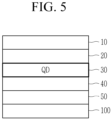
- a device according to an embodiment as shown in FIG. 5 has an inverted structure.
- a cathode 50 disposed on a transparent substrate 100 may include a metal oxide transparent electrode (e.g., ITO) and an anode 10 facing the cathode may include a metal (e.g., Au, Ag, etc.) of a predetermined (e.g., relatively high) work function.
- a metal oxide transparent electrode e.g., ITO
- an anode 10 facing the cathode may include a metal (e.g., Au, Ag, etc.) of a predetermined (e.g., relatively high) work function.
- an n-type metal oxide (ZnO) may be disposed between the transparent electrode 50 and the emission layer 30 as an electron auxiliary layer (e.g., an electron transport layer) 40.
- a hole auxiliary layer 20 (e.g., a hole transport layer including TFB and/or PVK and/or a hole injection layer including MoO 3 or another p-type metal oxide) may be disposed between the metal anode 10 and the quantum dot emission layer 30.
- a hole transport layer including TFB and/or PVK and/or a hole injection layer including MoO 3 or another p-type metal oxide may be disposed between the metal anode 10 and the quantum dot emission layer 30.
- Photoluminescence (PL) spectra of the produced nanocrystals are obtained using a Hitachi F-7000 spectrometer at an irradiation wavelength of 372 nanometers (nm).
- a UV spectroscopy analysis is performed by using a Hitachi U-3310 spectrometer to obtain a UV-Visible absorption spectrum.
- ICP-AES Inductively Coupled Plasma-Atomic Emission Spectroscopy
- ICP-AES inductively coupled plasma-atomic emission spectroscopy
- a synthesis is performed under an inert gas atmosphere (nitrogen flowing condition) unless particularly mentioned.
- TOP trioctylphosphine
- reaction solution is rapidly cooled down to room temperature, ethanol is added thereto, and the obtained mixture is centrifuged to recover ZnS core particles.
- the recovered ZnS core particles are dispersed in toluene.
- a mole ratio (hereinafter, also referred to as a ratio) between the used amounts of the zinc precursor and the sulfur precursor (Zn: S) is about 2:1.
- a transmission electron microscopic analysis is made for the core particles and the results confirm that the obtained core particles have a generally spherical shape and an average size thereof is about 2.6 nm.
- An ultraviolet-visible (UV-Vis) absorption spectroscopic analysis and a photoluminescent spectroscopic analysis are made and the results are shown in Table 1.
- the reaction solution is rapidly cooled down to room temperature, ethanol is added thereto, and the obtained mixture is centrifuged to recover core-shell particles.
- the recovered core-shell particles are dispersed in an organic solvent (e.g., toluene or octane).
- a selenium precursor solution, a sulfur precursor solution, and a zinc precursor solution are prepared in the same manner as set forth in Example 1.
- Tellurium is dispersed in trioctylphosphine (TOP) to prepare a 0.1 M Te/TOP stock solution.
- TOP trioctylphosphine
- a ratio among the Zn precursor: the Se precursor: the S precursor: the Te precursor is about 5:2:3:0.01.
- the reaction solution is rapidly cooled down to room temperature, ethanol is added thereto, and the obtained mixture is centrifuged to recover core-shell particles.
- the recovered core-shell particles are dispersed in an organic solvent (e.g., toluene or octane).
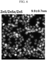
- a transmission electron microscopic analysis is carried out for the prepared semiconductor nanocrystal particles and the results are shown in FIG. 9 .
- the TEM analysis results confirm that the size of the semiconductor nanocrystal particles is about 9.9 ⁇ 0.6 nm and the shape distribution of the semiconductor nanocrystal particles is uniform.
- the EDS analysis and the image strength analysis results confirm that the prepared semiconductor nanocrystal particles have the ZnS core and the ZnS outermost shell layer.
- a selenium precursor solution, a sulfur precursor solution, and a zinc precursor solution are prepared in the same manner as set forth in Example 1.
- Tellurium is dispersed in trioctylphosphine (TOP) to prepare a 0.1 M Te/TOP stock solution.
- TOP trioctylphosphine
- a selenium precursor solution, a sulfur precursor solution, and a zinc precursor solution are prepared in the same manner as set forth in Example 1.
- reaction solution is rapidly cooled down to room temperature, ethanol is added thereto, and the obtained mixture is centrifuged to recover ZnSe core particles.
- the recovered ZnSe core particles are dispersed in toluene.
- a ratio among the Zn precursor: the Se precursor: the Te precursor is about 2:1.
- trioctylamine is placed and zinc acetate and oleic acid are added thereto and vacuum-treated at 120 °C.
- the atmosphere in the flask is changed into nitrogen (N 2 ).
- N 2 nitrogen
- a toluene dispersion of the ZnSe core is injected quickly and then the S/TOP stock solution is added thereto.
- the reaction proceeds about 1 hour to form a ZnS layer on the core.
- a ratio among the Zn precursor: the S precursor is about 1:2.
- the reaction solution is rapidly cooled down to room temperature, ethanol is added thereto, and the obtained mixture is centrifuged to recover core-shell particles.
- the recovered core-shell particles are dispersed in an organic solvent (e.g., toluene or octane).
- a photoluminescent efficiency is measured at the excitation light wavelength of 372 nm for each of the toluene dispersion of the semiconductor nanocrystal particles prepared in Example 2, the toluene dispersion of the semiconductor nanocrystal particles prepared in Comparative Example 1, and the toluene dispersion of the semiconductor nanocrystal particles prepared in Comparative Example 2.
- the dispersions are left in air at a temperature of about 25 °C, a PL efficiency of each of them is measured respectively.
- the results confirm that the semiconductor nanocrystal particles prepared in Example 2 may have a maintenance ratio of the PL efficiency 2.5 times and 2 times higher than a maintenance ratio of the PL efficiency of the semiconductor nanocrystal particles prepared in Comparative Example 2 and Comparative Example 1, respectively.
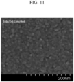
- Each of the octane dispersion of the semiconductor nanocrystal particles prepared in Example 1 and the octane dispersion of the semiconductor nanocrystal particles prepared in Comparative Example 2 is spin-coated on a glass substrate to form a layer of the quantum dots.
- the layers of the quantum dots are observed with a transmission electron microscope and the results are shown in FIG. 10 (for the semiconductor nanocrystal particles prepared in Example 1) and FIG. 11 (for the semiconductor nanocrystal particles prepared in Comparative Example 2), respectively.
- FIG. 10 and FIG. 11 confirm that the thin film of the semiconductor nanocrystal particles of Example 1 may show improved uniformity in comparison with that of the semiconductor nanocrystal particles of Comparative Example 2.
Landscapes
- Chemical & Material Sciences (AREA)
- Engineering & Computer Science (AREA)
- Organic Chemistry (AREA)
- Inorganic Chemistry (AREA)
- Materials Engineering (AREA)
- Nanotechnology (AREA)
- Crystallography & Structural Chemistry (AREA)
- Physics & Mathematics (AREA)
- Optics & Photonics (AREA)
- Condensed Matter Physics & Semiconductors (AREA)
- General Physics & Mathematics (AREA)
- Metallurgy (AREA)
- Manufacturing & Machinery (AREA)
- Composite Materials (AREA)
- Life Sciences & Earth Sciences (AREA)
- Biophysics (AREA)
- Luminescent Compositions (AREA)
- Electroluminescent Light Sources (AREA)
- Inorganic Compounds Of Heavy Metals (AREA)
- Led Device Packages (AREA)
Claims (14)
- Halbleiternanokristallpartikel, umfassend:einen Kern, umfassendeinen ersten Halbleiternanokristall,eine erste Schale, die den Kern umgibt, wobei die erste Schale einen zweiten Halbleiternanokristall umfasst, der eine andere Zusammensetzung als der erste Halbleiternanokristall aufweist, undeine zweite Schale, die die erste Schale umgibt, wobei die zweite Schale einen dritten Halbleiternanokristall umfasst, der eine andere Zusammensetzung als der zweite Halbleiternanokristall aufweist,wobei der erste Halbleiternanokristall Zink und Schwefel umfasst;wobei der zweite Halbleiternanokristall Zink und Selen umfasst;wobei der dritte Halbleiternanokristall Zink und Schwefel umfasst;wobei eine Energiebandlücke des zweiten Halbleiternanokristalls kleiner ist als eine Energiebandlücke des ersten Halbleiternanokristalls, und die Energiebandlücke des zweiten Halbleiternanokristalls kleiner ist als eine Energiebandlücke des dritten Halbleiternanokristalls;wobei das Halbleiternanokristallpartikel kein Cadmium umfasst;wobei ein maximaler Photolumineszenz-Peak des Halbleiternanokristallpartikels in einem Bereich zwischen 400 Nanometern und 500 Nanometern vorhanden ist; undwobei eine Quanteneffizienz des Halbleiternanokristallpartikels größer oder gleich 60 % ist.
- Halbleiternanokristallpartikel nach Anspruch 1, wobei die Energiebandlücke des ersten Halbleiternanokristalls kleiner oder gleich der Energiebandlücke des dritten Halbleiternanokristalls ist.
- Halbleiternanokristallpartikel nach Anspruch 1 oder 2, wobei der Kern, die erste Schale und die zweite Schale eine Verbindung von Gruppe II-VI umfassen.
- Halbleiternanokristallpartikel nach einem der vorhergehenden Ansprüche, wobei der erste Halbleiternanokristall ZnS, ZnSeS oder eine Kombination davon umfasst und/oder wobei der zweite Halbleiternanokristall ZnSe, ZnSeS, ZnSeTe oder eine Kombination davon umfasst.
- Halbleiternanokristallpartikel nach einem der vorhergehenden Ansprüche, wobei der erste Halbleiternanokristall kein(e) Kupfer, Mangan oder Kombination davon umfasst.
- Halbleiternanokristallpartikel nach einem der vorhergehenden Ansprüche, wobei die erste Schale eine Vielzahl von Schichten umfasst und in der Vielzahl von Schichten benachbarte Schichten Halbleiternanokristalle von voneinander unterschiedlichen Zusammensetzungen umfassen, undwobei optional die erste Schale eine erste Schicht und eine zweite Schicht umfasst und eine Energiebandlücke des Halbleiternanokristalls in der ersten Schicht kleiner ist als eine Energiebandlücke des Halbleiternanokristalls in der zweiten Schicht, undwobei ferner optional die erste Schicht ZnSeTe umfasst und die zweite Schicht ZnSe umfasst.
- Halbleiternanokristallpartikel nach einem der vorhergehenden Ansprüche, wobei der dritte Halbleiternanokristall ZnS umfasst.
- Halbleiternanokristallpartikel nach einem der vorhergehenden Ansprüche, wobei ein maximaler Photolumineszenz-Peak des Halbleiternanokristallpartikels in einem Bereich zwischen 416 Nanometern und 470 Nanometern vorhanden ist.
- Halbleiternanokristallpartikel nach einem der vorhergehenden Ansprüche, wobei ein maximaler Photolumineszenz-Peak des Halbleiternanokristallpartikels eine Halbwertsbreite von weniger als oder gleich 40 Nanometern aufweist.
- Halbleiternanokristallpartikel nach einem der vorhergehenden Ansprüche, wobei ein maximaler Photolumineszenz-Peak des Halbleiternanokristallpartikels eine Halbwertsbreite von weniger als oder gleich 30 Nanometern aufweist.
- Quantenpunktpopulation, die eine Vielzahl von Halbleiternanokristallpartikeln umfasst, wobei die Vielzahl von Halbleiternanokristallpartikeln ein Halbleiternanokristallpartikel nach einem der vorhergehenden Ansprüche umfasst und wobei eine durchschnittliche Größe der Vielzahl von Halbleiternanokristallpartikeln größer oder gleich 5 Nanometer und kleiner oder gleich 50 Nanometer ist,wobei die Größe eines Halbleiternanokristallpartikels ein Durchmesser ist, wenn der Halbleiternanokristallpartikel eine Kugelform aufweist, oder die Größe eines Halbleiternanokristallpartikels ein Durchmesser eines Kreises mit gleicher Fläche ist, berechnet aus einem zweidimensionalen Bereich eines elektronenmikroskopischen Bildes des Partikels, undwobei optional eine Standardabweichung der Größen der Vielzahl von Halbleiternanokristallpartikeln kleiner oder gleich 10 % ist.
- Verfahren zur Herstellung des Halbleiternanokristallpartikels nach einem der vorhergehenden Ansprüche, das Verfahren umfassendBereitstellen eines Kernpartikels, das den Kern umfasst, wobei der Kern den ersten Halbleiternanokristall umfasst;Durchführen einer Reaktion zwischen einem zweiten Metallvorläufer und einem zweiten Nichtmetallvorläufer des zweiten Halbleiternanokristalls in Gegenwart des Kernpartikels, eines organischen Lösungsmittels und eines organischen Liganden, um eine Reaktionslösung zu erhalten, die ein Partikel umfasst, das die erste Schale umfasst, die den zweiten Halbleiternanokristall auf dem Kernpartikel umfasst;Zugeben eines dritten Metallvorläufers und eines dritten Nichtmetallvorläufers des dritten Halbleiternanokristalls zu der Reaktionslösung, um eine Reaktion dazwischen durchzuführen, um das Halbleiternanokristallpartikel zu erhalten, das die zweite Schale umfasst, die den auf der ersten Schale gebildeten dritten Halbleiternanokristall umfasst, und wobei optional das Bilden der ersten Schale das Erwärmen eines Gemischs aus dem organischen Lösungsmittel, dem organischen Liganden und dem zweiten Metallvorläufer auf eine erste Reaktionstemperatur und das Zugeben des Kernpartikels und des zweiten Nichtmetallvorläufers zu dem auf die erste Reaktionstemperatur erwärmten Gemischs umfasst.
- Licht emittierende Vorrichtung, umfassend:eine erste Elektrode und eine zweite Elektrode, die einander zugewandt sind, undeine Quantenpunktlicht emittierende Schicht, die zwischen der ersten Elektrode und der zweiten Elektrode angeordnet ist, wobei die Quantenpunktlicht emittierende Schicht eine Vielzahl von Quantenpunkten umfasst, wobei die Vielzahl von Quantenpunkten ein Halbleiternanokristallpartikel nach einem der Ansprüchen 1 bis 10 umfasst.
- Licht emittierende Vorrichtung nach Anspruch 13, wobei die Vorrichtung ferner eine Ladungshilfsschicht zwischen der ersten Elektrode und der Quantenpunktlicht emittierenden Schicht, zwischen der zweiten Elektrode und der Quantenpunktlicht emittierenden Schicht oder zwischen der ersten Elektrode und der Quantenpunktlicht emittierenden Schicht und zwischen der zweiten Elektrode und der Quantenpunktlicht emittierenden Schicht umfasst, und wobei optional die Ladungshilfsschicht eine Ladungstransportschicht, eine Ladungsinjektionsschicht oder die Ladungstransportschicht und die Ladungsinjektionsschicht umfasst.
Applications Claiming Priority (1)
| Application Number | Priority Date | Filing Date | Title |
|---|---|---|---|
| KR20180020799 | 2018-02-21 |
Publications (2)
| Publication Number | Publication Date |
|---|---|
| EP3530713A1 EP3530713A1 (de) | 2019-08-28 |
| EP3530713B1 true EP3530713B1 (de) | 2025-04-02 |
Family
ID=65529443
Family Applications (1)
| Application Number | Title | Priority Date | Filing Date |
|---|---|---|---|
| EP19158388.9A Active EP3530713B1 (de) | 2018-02-21 | 2019-02-20 | Halbleiternanokristallpartikel, herstellungsverfahren dafür und vorrichtungen damit |
Country Status (5)
| Country | Link |
|---|---|
| US (2) | US11566345B2 (de) |
| EP (1) | EP3530713B1 (de) |
| JP (1) | JP7235530B2 (de) |
| KR (1) | KR102718894B1 (de) |
| CN (1) | CN110172348B (de) |
Families Citing this family (26)
| Publication number | Priority date | Publication date | Assignee | Title |
|---|---|---|---|---|
| KR102618410B1 (ko) | 2017-05-11 | 2023-12-27 | 삼성전자주식회사 | 반도체 나노결정 입자 및 이를 포함하는 소자 |
| EP3530713B1 (de) * | 2018-02-21 | 2025-04-02 | Samsung Electronics Co., Ltd. | Halbleiternanokristallpartikel, herstellungsverfahren dafür und vorrichtungen damit |
| CN109370564B (zh) * | 2018-10-26 | 2026-03-13 | 纳晶科技股份有限公司 | 一种蓝光量子点及其制备方法、电子器件 |
| US11149199B2 (en) * | 2018-11-23 | 2021-10-19 | Samsung Display Co., Ltd. | Quantum dots, compositions and composites including the same, and electronic device including the same |
| US12029058B2 (en) * | 2019-03-11 | 2024-07-02 | Sharp Kabushiki Kaisha | Light emitting element and display device using same |
| WO2020208671A1 (ja) * | 2019-04-08 | 2020-10-15 | シャープ株式会社 | 表示デバイス |
| US20220199926A1 (en) * | 2019-04-17 | 2022-06-23 | Sharp Kabushiki Kaisha | Electroluminescence element, display device, and method for producing electroluminescence element |
| KR102652436B1 (ko) | 2019-04-18 | 2024-03-27 | 삼성전자주식회사 | ZnTeSe 기반의 양자점 |
| KR102711311B1 (ko) | 2019-04-18 | 2024-09-26 | 삼성전자주식회사 | 리튬 함유 무카드뮴 양자점, 그 제조 방법, 및 이를 포함하는 전자 소자 |
| KR102711312B1 (ko) * | 2019-04-18 | 2024-09-26 | 삼성전자주식회사 | 코어쉘 양자점, 그 제조 방법, 및 이를 포함하는 전자 소자 |
| US11499097B2 (en) * | 2019-08-12 | 2022-11-15 | Nanosys, Inc. | Synthesis of blue-emitting ZnSe1-xTex alloy nanocrystals with low full width at half-maximum |
| CN112442371B (zh) * | 2019-08-29 | 2024-04-12 | 三星电子株式会社 | 量子点、其制造方法、包括其的量子点群和电致发光器件 |
| EP4032850A4 (de) | 2019-09-20 | 2023-10-04 | NS Materials Inc. | Quantenpunkt und verfahren zur herstellung davon |
| KR102712542B1 (ko) * | 2019-10-07 | 2024-09-30 | 삼성전자주식회사 | 전계 발광 소자 및 이를 포함하는 표시 장치 |
| US11603493B2 (en) * | 2019-10-17 | 2023-03-14 | Samsung Electronics Co., Ltd. | Core shell quantum dot, production method thereof, and electronic device including the same |
| KR102824530B1 (ko) | 2019-10-17 | 2025-06-24 | 삼성전자주식회사 | 코어쉘 양자점, 그 제조 방법, 및 이를 포함하는 전자 소자 |
| CN111081904A (zh) * | 2019-12-02 | 2020-04-28 | 武汉华星光电半导体显示技术有限公司 | 氧化石墨烯薄膜的制备方法、oled器件及制备方法 |
| CN114746363B (zh) * | 2019-12-02 | 2024-12-13 | 信越化学工业株式会社 | 量子点、波长转换材料、背光单元、图像显示装置及量子点的制造方法 |
| CN113130631B (zh) * | 2019-12-30 | 2022-11-29 | Tcl科技集团股份有限公司 | 一种异质结纳米材料及其制备方法、薄膜、量子点发光二极管 |
| KR102753925B1 (ko) * | 2020-08-18 | 2025-01-15 | 삼성디스플레이 주식회사 | 반도체 나노입자 및 이를 포함한 전자 장치 |
| US20230413589A1 (en) * | 2020-10-14 | 2023-12-21 | Sharp Kabushiki Kaisha | Light-emitting element |
| KR102856154B1 (ko) * | 2020-10-16 | 2025-09-04 | 삼성전자주식회사 | 양자점, 그 제조 방법, 및 이를 포함하는 전자 소자 |
| CN114806540A (zh) * | 2021-01-20 | 2022-07-29 | 三星显示有限公司 | 量子点及包含量子点的油墨组合物、光学构件和电子器件 |
| US20240107792A1 (en) * | 2021-02-18 | 2024-03-28 | Sharp Kabushiki Kaisha | Electroluminescent element |
| KR20230112195A (ko) * | 2022-01-19 | 2023-07-27 | 삼성디스플레이 주식회사 | 양자점을 포함한 발광 소자 및 상기 발광 소자를 포함한 전자 장치 |
| WO2025131983A1 (en) * | 2023-12-21 | 2025-06-26 | Ams-Osram International Gmbh | Structure, method for producing a structure and optoelectronic device |
Family Cites Families (20)
| Publication number | Priority date | Publication date | Assignee | Title |
|---|---|---|---|---|
| US6607829B1 (en) * | 1997-11-13 | 2003-08-19 | Massachusetts Institute Of Technology | Tellurium-containing nanocrystalline materials |
| US7534488B2 (en) * | 2003-09-10 | 2009-05-19 | The Regents Of The University Of California | Graded core/shell semiconductor nanorods and nanorod barcodes |
| WO2004066361A2 (en) * | 2003-01-22 | 2004-08-05 | The Board Of Trustees Of The University Of Arkansas | Monodisperse core/shell and other complex structured nanocrystals and methods of preparing the same |
| GB2472542B (en) * | 2005-08-12 | 2011-03-23 | Nanoco Technologies Ltd | Nanoparticles |
| WO2008063652A1 (en) * | 2006-11-21 | 2008-05-29 | Qd Vision, Inc. | Blue emitting semiconductor nanocrystals and compositions and devices including same |
| KR101711085B1 (ko) | 2009-10-09 | 2017-03-14 | 삼성전자 주식회사 | 나노 복합 입자, 그 제조방법 및 상기 나노 복합 입자를 포함하는 소자 |
| KR101738551B1 (ko) | 2010-06-24 | 2017-05-23 | 삼성전자주식회사 | 반도체 나노 결정 |
| US8702277B2 (en) | 2010-07-12 | 2014-04-22 | Samsung Electronics Co., Ltd. | White light emitting diode and liquid crystal display including the same |
| CN102086396B (zh) * | 2010-11-25 | 2013-12-04 | 华北电力大学 | 一种CuInS2-ZnS/ZnSe/ZnS核壳结构半导体量子点的制备方法及其在发光器件中的应用 |
| WO2014089743A1 (en) | 2012-12-10 | 2014-06-19 | East China University Of Science And Technology | One step synthesis of core/shell nanocrystal quantum dots |
| DE102013206077A1 (de) | 2013-04-05 | 2014-10-09 | Fraunhofer-Gesellschaft zur Förderung der angewandten Forschung e.V. | Blau-emittierende Leuchtdioden auf Basis von Zinkselenid-Quantenpunkten |
| KR101575572B1 (ko) * | 2014-04-16 | 2015-12-10 | 경북대학교 산학협력단 | 발광 소자 및 발광 소자 제조 방법 |
| JP6697272B2 (ja) | 2015-01-19 | 2020-05-20 | スタンレー電気株式会社 | コアシェル構造を有する量子ドットとその製造方法 |
| CN104987860B (zh) | 2015-07-24 | 2017-03-01 | 东南大学 | 共掺型与分掺型ZnInS/ZnS双发射量子点的制备方法 |
| WO2017044597A1 (en) * | 2015-09-09 | 2017-03-16 | Truskier Jonathan | Highly luminescent cadmium-free nanocrystals with blue emission |
| KR102415248B1 (ko) | 2015-12-29 | 2022-06-30 | 삼성디스플레이 주식회사 | 양자점 및 이를 이용한 발광 소자 |
| WO2017204193A1 (ja) * | 2016-05-27 | 2017-11-30 | 富士フイルム株式会社 | コアシェル粒子、コアシェル粒子の製造方法およびフィルム |
| KR102689815B1 (ko) * | 2016-11-15 | 2024-07-29 | 엘지디스플레이 주식회사 | 양자점 발광다이오드 및 이를 이용한 발광 표시장치 |
| CN106753326A (zh) | 2016-11-21 | 2017-05-31 | 北京科技大学 | M:ZnSe/ZnSe/ZnS结构量子点制备方法 |
| EP3530713B1 (de) * | 2018-02-21 | 2025-04-02 | Samsung Electronics Co., Ltd. | Halbleiternanokristallpartikel, herstellungsverfahren dafür und vorrichtungen damit |
-
2019
- 2019-02-20 EP EP19158388.9A patent/EP3530713B1/de active Active
- 2019-02-21 KR KR1020190020763A patent/KR102718894B1/ko active Active
- 2019-02-21 JP JP2019029208A patent/JP7235530B2/ja active Active
- 2019-02-21 CN CN201910140377.XA patent/CN110172348B/zh active Active
- 2019-02-21 US US16/281,232 patent/US11566345B2/en active Active
-
2022
- 2022-11-04 US US18/052,597 patent/US11982018B2/en active Active
Also Published As
| Publication number | Publication date |
|---|---|
| US11566345B2 (en) | 2023-01-31 |
| CN110172348A (zh) | 2019-08-27 |
| CN110172348B (zh) | 2023-12-01 |
| KR20190100885A (ko) | 2019-08-29 |
| US20230093467A1 (en) | 2023-03-23 |
| JP7235530B2 (ja) | 2023-03-08 |
| US20190257003A1 (en) | 2019-08-22 |
| KR102718894B1 (ko) | 2024-10-17 |
| EP3530713A1 (de) | 2019-08-28 |
| US11982018B2 (en) | 2024-05-14 |
| JP2019145505A (ja) | 2019-08-29 |
Similar Documents
| Publication | Publication Date | Title |
|---|---|---|
| US11982018B2 (en) | Semiconductor nanocrystal particles of core-shell structure having specific bandgap relationship between the core and the shells, production methods thereof, and devices including the same | |
| US11981852B2 (en) | Quantum dots and devices including the same | |
| US12060510B2 (en) | Semiconductor nanocrystal particles and devices including the same | |
| EP3536761B1 (de) | Quantenpunkte | |
| US11011720B2 (en) | Semiconductor nanocrystal particles, production methods thereof, and devices including the same | |
| KR102807529B1 (ko) | 양자점 소자 및 양자점 | |
| US12187941B2 (en) | Core shell quantum dot and electronic device including the same | |
| US11981850B2 (en) | Quantum dots, and an electronic device including the same | |
| EP3933008B1 (de) | Quantenpunkte und vorrichtungen damit |
Legal Events
| Date | Code | Title | Description |
|---|---|---|---|
| PUAI | Public reference made under article 153(3) epc to a published international application that has entered the european phase |
Free format text: ORIGINAL CODE: 0009012 |
|
| STAA | Information on the status of an ep patent application or granted ep patent |
Free format text: STATUS: THE APPLICATION HAS BEEN PUBLISHED |
|
| AK | Designated contracting states |
Kind code of ref document: A1 Designated state(s): AL AT BE BG CH CY CZ DE DK EE ES FI FR GB GR HR HU IE IS IT LI LT LU LV MC MK MT NL NO PL PT RO RS SE SI SK SM TR |
|
| AX | Request for extension of the european patent |
Extension state: BA ME |
|
| STAA | Information on the status of an ep patent application or granted ep patent |
Free format text: STATUS: REQUEST FOR EXAMINATION WAS MADE |
|
| 17P | Request for examination filed |
Effective date: 20200228 |
|
| RBV | Designated contracting states (corrected) |
Designated state(s): AL AT BE BG CH CY CZ DE DK EE ES FI FR GB GR HR HU IE IS IT LI LT LU LV MC MK MT NL NO PL PT RO RS SE SI SK SM TR |
|
| STAA | Information on the status of an ep patent application or granted ep patent |
Free format text: STATUS: EXAMINATION IS IN PROGRESS |
|
| 17Q | First examination report despatched |
Effective date: 20230328 |
|
| P01 | Opt-out of the competence of the unified patent court (upc) registered |
Effective date: 20230520 |
|
| GRAP | Despatch of communication of intention to grant a patent |
Free format text: ORIGINAL CODE: EPIDOSNIGR1 |
|
| STAA | Information on the status of an ep patent application or granted ep patent |
Free format text: STATUS: GRANT OF PATENT IS INTENDED |
|
| INTG | Intention to grant announced |
Effective date: 20241004 |
|
| GRAS | Grant fee paid |
Free format text: ORIGINAL CODE: EPIDOSNIGR3 |
|
| GRAA | (expected) grant |
Free format text: ORIGINAL CODE: 0009210 |
|
| STAA | Information on the status of an ep patent application or granted ep patent |
Free format text: STATUS: THE PATENT HAS BEEN GRANTED |
|
| AK | Designated contracting states |
Kind code of ref document: B1 Designated state(s): AL AT BE BG CH CY CZ DE DK EE ES FI FR GB GR HR HU IE IS IT LI LT LU LV MC MK MT NL NO PL PT RO RS SE SI SK SM TR |
|
| REG | Reference to a national code |
Ref country code: GB Ref legal event code: FG4D |
|
| REG | Reference to a national code |
Ref country code: CH Ref legal event code: EP |
|
| REG | Reference to a national code |
Ref country code: IE Ref legal event code: FG4D |
|
| REG | Reference to a national code |
Ref country code: DE Ref legal event code: R096 Ref document number: 602019068006 Country of ref document: DE |
|
| REG | Reference to a national code |
Ref country code: NL Ref legal event code: MP Effective date: 20250402 |
|
| PG25 | Lapsed in a contracting state [announced via postgrant information from national office to epo] |
Ref country code: NL Free format text: LAPSE BECAUSE OF FAILURE TO SUBMIT A TRANSLATION OF THE DESCRIPTION OR TO PAY THE FEE WITHIN THE PRESCRIBED TIME-LIMIT Effective date: 20250402 |
|
| REG | Reference to a national code |
Ref country code: AT Ref legal event code: MK05 Ref document number: 1781276 Country of ref document: AT Kind code of ref document: T Effective date: 20250402 |
|
| PG25 | Lapsed in a contracting state [announced via postgrant information from national office to epo] |
Ref country code: FI Free format text: LAPSE BECAUSE OF FAILURE TO SUBMIT A TRANSLATION OF THE DESCRIPTION OR TO PAY THE FEE WITHIN THE PRESCRIBED TIME-LIMIT Effective date: 20250402 Ref country code: ES Free format text: LAPSE BECAUSE OF FAILURE TO SUBMIT A TRANSLATION OF THE DESCRIPTION OR TO PAY THE FEE WITHIN THE PRESCRIBED TIME-LIMIT Effective date: 20250402 Ref country code: PT Free format text: LAPSE BECAUSE OF FAILURE TO SUBMIT A TRANSLATION OF THE DESCRIPTION OR TO PAY THE FEE WITHIN THE PRESCRIBED TIME-LIMIT Effective date: 20250804 |
|
| REG | Reference to a national code |
Ref country code: LT Ref legal event code: MG9D |
|
| PG25 | Lapsed in a contracting state [announced via postgrant information from national office to epo] |
Ref country code: GR Free format text: LAPSE BECAUSE OF FAILURE TO SUBMIT A TRANSLATION OF THE DESCRIPTION OR TO PAY THE FEE WITHIN THE PRESCRIBED TIME-LIMIT Effective date: 20250703 Ref country code: NO Free format text: LAPSE BECAUSE OF FAILURE TO SUBMIT A TRANSLATION OF THE DESCRIPTION OR TO PAY THE FEE WITHIN THE PRESCRIBED TIME-LIMIT Effective date: 20250702 |
|
| PG25 | Lapsed in a contracting state [announced via postgrant information from national office to epo] |
Ref country code: PL Free format text: LAPSE BECAUSE OF FAILURE TO SUBMIT A TRANSLATION OF THE DESCRIPTION OR TO PAY THE FEE WITHIN THE PRESCRIBED TIME-LIMIT Effective date: 20250402 |
|
| PG25 | Lapsed in a contracting state [announced via postgrant information from national office to epo] |
Ref country code: BG Free format text: LAPSE BECAUSE OF FAILURE TO SUBMIT A TRANSLATION OF THE DESCRIPTION OR TO PAY THE FEE WITHIN THE PRESCRIBED TIME-LIMIT Effective date: 20250402 |
|
| PG25 | Lapsed in a contracting state [announced via postgrant information from national office to epo] |
Ref country code: HR Free format text: LAPSE BECAUSE OF FAILURE TO SUBMIT A TRANSLATION OF THE DESCRIPTION OR TO PAY THE FEE WITHIN THE PRESCRIBED TIME-LIMIT Effective date: 20250402 |
|
| PG25 | Lapsed in a contracting state [announced via postgrant information from national office to epo] |
Ref country code: AT Free format text: LAPSE BECAUSE OF FAILURE TO SUBMIT A TRANSLATION OF THE DESCRIPTION OR TO PAY THE FEE WITHIN THE PRESCRIBED TIME-LIMIT Effective date: 20250402 |
|
| PG25 | Lapsed in a contracting state [announced via postgrant information from national office to epo] |
Ref country code: RS Free format text: LAPSE BECAUSE OF FAILURE TO SUBMIT A TRANSLATION OF THE DESCRIPTION OR TO PAY THE FEE WITHIN THE PRESCRIBED TIME-LIMIT Effective date: 20250702 |
|
| PG25 | Lapsed in a contracting state [announced via postgrant information from national office to epo] |
Ref country code: IS Free format text: LAPSE BECAUSE OF FAILURE TO SUBMIT A TRANSLATION OF THE DESCRIPTION OR TO PAY THE FEE WITHIN THE PRESCRIBED TIME-LIMIT Effective date: 20250802 |
|
| PG25 | Lapsed in a contracting state [announced via postgrant information from national office to epo] |
Ref country code: LV Free format text: LAPSE BECAUSE OF FAILURE TO SUBMIT A TRANSLATION OF THE DESCRIPTION OR TO PAY THE FEE WITHIN THE PRESCRIBED TIME-LIMIT Effective date: 20250402 |
|
| REG | Reference to a national code |
Ref country code: DE Ref legal event code: R097 Ref document number: 602019068006 Country of ref document: DE |
|
| PG25 | Lapsed in a contracting state [announced via postgrant information from national office to epo] |
Ref country code: DK Free format text: LAPSE BECAUSE OF FAILURE TO SUBMIT A TRANSLATION OF THE DESCRIPTION OR TO PAY THE FEE WITHIN THE PRESCRIBED TIME-LIMIT Effective date: 20250402 Ref country code: SM Free format text: LAPSE BECAUSE OF FAILURE TO SUBMIT A TRANSLATION OF THE DESCRIPTION OR TO PAY THE FEE WITHIN THE PRESCRIBED TIME-LIMIT Effective date: 20250402 |
|
| PG25 | Lapsed in a contracting state [announced via postgrant information from national office to epo] |
Ref country code: CZ Free format text: LAPSE BECAUSE OF FAILURE TO SUBMIT A TRANSLATION OF THE DESCRIPTION OR TO PAY THE FEE WITHIN THE PRESCRIBED TIME-LIMIT Effective date: 20250402 |
|
| PG25 | Lapsed in a contracting state [announced via postgrant information from national office to epo] |
Ref country code: EE Free format text: LAPSE BECAUSE OF FAILURE TO SUBMIT A TRANSLATION OF THE DESCRIPTION OR TO PAY THE FEE WITHIN THE PRESCRIBED TIME-LIMIT Effective date: 20250402 |
|
| PG25 | Lapsed in a contracting state [announced via postgrant information from national office to epo] |
Ref country code: SK Free format text: LAPSE BECAUSE OF FAILURE TO SUBMIT A TRANSLATION OF THE DESCRIPTION OR TO PAY THE FEE WITHIN THE PRESCRIBED TIME-LIMIT Effective date: 20250402 Ref country code: RO Free format text: LAPSE BECAUSE OF FAILURE TO SUBMIT A TRANSLATION OF THE DESCRIPTION OR TO PAY THE FEE WITHIN THE PRESCRIBED TIME-LIMIT Effective date: 20250402 |
|
| PG25 | Lapsed in a contracting state [announced via postgrant information from national office to epo] |
Ref country code: IT Free format text: LAPSE BECAUSE OF FAILURE TO SUBMIT A TRANSLATION OF THE DESCRIPTION OR TO PAY THE FEE WITHIN THE PRESCRIBED TIME-LIMIT Effective date: 20250402 |
|
| PLBE | No opposition filed within time limit |
Free format text: ORIGINAL CODE: 0009261 |
|
| STAA | Information on the status of an ep patent application or granted ep patent |
Free format text: STATUS: NO OPPOSITION FILED WITHIN TIME LIMIT |
|
| REG | Reference to a national code |
Ref country code: CH Ref legal event code: L10 Free format text: ST27 STATUS EVENT CODE: U-0-0-L10-L00 (AS PROVIDED BY THE NATIONAL OFFICE) Effective date: 20260211 |
|
| 26N | No opposition filed |
Effective date: 20260105 |