EP3518294B1 - Solarzellenmodul mit einem verdrahtungsleitungsmaterial zur verbindung von solarzellen - Google Patents
Solarzellenmodul mit einem verdrahtungsleitungsmaterial zur verbindung von solarzellen Download PDFInfo
- Publication number
- EP3518294B1 EP3518294B1 EP17852644.8A EP17852644A EP3518294B1 EP 3518294 B1 EP3518294 B1 EP 3518294B1 EP 17852644 A EP17852644 A EP 17852644A EP 3518294 B1 EP3518294 B1 EP 3518294B1
- Authority
- EP
- European Patent Office
- Prior art keywords
- solar cell
- wiring member
- light
- cell module
- disposed
- Prior art date
- Legal status (The legal status is an assumption and is not a legal conclusion. Google has not performed a legal analysis and makes no representation as to the accuracy of the status listed.)
- Active
Links
Images



Classifications
-
- H—ELECTRICITY
- H10—SEMICONDUCTOR DEVICES; ELECTRIC SOLID-STATE DEVICES NOT OTHERWISE PROVIDED FOR
- H10F—INORGANIC SEMICONDUCTOR DEVICES SENSITIVE TO INFRARED RADIATION, LIGHT, ELECTROMAGNETIC RADIATION OF SHORTER WAVELENGTH OR CORPUSCULAR RADIATION
- H10F19/00—Integrated devices, or assemblies of multiple devices, comprising at least one photovoltaic cell covered by group H10F10/00, e.g. photovoltaic modules
- H10F19/80—Encapsulations or containers for integrated devices, or assemblies of multiple devices, having photovoltaic cells
-
- H—ELECTRICITY
- H10—SEMICONDUCTOR DEVICES; ELECTRIC SOLID-STATE DEVICES NOT OTHERWISE PROVIDED FOR
- H10F—INORGANIC SEMICONDUCTOR DEVICES SENSITIVE TO INFRARED RADIATION, LIGHT, ELECTROMAGNETIC RADIATION OF SHORTER WAVELENGTH OR CORPUSCULAR RADIATION
- H10F19/00—Integrated devices, or assemblies of multiple devices, comprising at least one photovoltaic cell covered by group H10F10/00, e.g. photovoltaic modules
- H10F19/80—Encapsulations or containers for integrated devices, or assemblies of multiple devices, having photovoltaic cells
- H10F19/85—Protective back sheets
-
- H—ELECTRICITY
- H10—SEMICONDUCTOR DEVICES; ELECTRIC SOLID-STATE DEVICES NOT OTHERWISE PROVIDED FOR
- H10F—INORGANIC SEMICONDUCTOR DEVICES SENSITIVE TO INFRARED RADIATION, LIGHT, ELECTROMAGNETIC RADIATION OF SHORTER WAVELENGTH OR CORPUSCULAR RADIATION
- H10F19/00—Integrated devices, or assemblies of multiple devices, comprising at least one photovoltaic cell covered by group H10F10/00, e.g. photovoltaic modules
- H10F19/90—Structures for connecting between photovoltaic cells, e.g. interconnections or insulating spacers
-
- H—ELECTRICITY
- H10—SEMICONDUCTOR DEVICES; ELECTRIC SOLID-STATE DEVICES NOT OTHERWISE PROVIDED FOR
- H10F—INORGANIC SEMICONDUCTOR DEVICES SENSITIVE TO INFRARED RADIATION, LIGHT, ELECTROMAGNETIC RADIATION OF SHORTER WAVELENGTH OR CORPUSCULAR RADIATION
- H10F19/00—Integrated devices, or assemblies of multiple devices, comprising at least one photovoltaic cell covered by group H10F10/00, e.g. photovoltaic modules
- H10F19/90—Structures for connecting between photovoltaic cells, e.g. interconnections or insulating spacers
- H10F19/902—Structures for connecting between photovoltaic cells, e.g. interconnections or insulating spacers for series or parallel connection of photovoltaic cells
- H10F19/904—Structures for connecting between photovoltaic cells, e.g. interconnections or insulating spacers for series or parallel connection of photovoltaic cells characterised by the shapes of the structures
-
- H—ELECTRICITY
- H10—SEMICONDUCTOR DEVICES; ELECTRIC SOLID-STATE DEVICES NOT OTHERWISE PROVIDED FOR
- H10F—INORGANIC SEMICONDUCTOR DEVICES SENSITIVE TO INFRARED RADIATION, LIGHT, ELECTROMAGNETIC RADIATION OF SHORTER WAVELENGTH OR CORPUSCULAR RADIATION
- H10F19/00—Integrated devices, or assemblies of multiple devices, comprising at least one photovoltaic cell covered by group H10F10/00, e.g. photovoltaic modules
- H10F19/90—Structures for connecting between photovoltaic cells, e.g. interconnections or insulating spacers
- H10F19/902—Structures for connecting between photovoltaic cells, e.g. interconnections or insulating spacers for series or parallel connection of photovoltaic cells
- H10F19/906—Structures for connecting between photovoltaic cells, e.g. interconnections or insulating spacers for series or parallel connection of photovoltaic cells characterised by the materials of the structures
-
- H—ELECTRICITY
- H10—SEMICONDUCTOR DEVICES; ELECTRIC SOLID-STATE DEVICES NOT OTHERWISE PROVIDED FOR
- H10F—INORGANIC SEMICONDUCTOR DEVICES SENSITIVE TO INFRARED RADIATION, LIGHT, ELECTROMAGNETIC RADIATION OF SHORTER WAVELENGTH OR CORPUSCULAR RADIATION
- H10F19/00—Integrated devices, or assemblies of multiple devices, comprising at least one photovoltaic cell covered by group H10F10/00, e.g. photovoltaic modules
- H10F19/90—Structures for connecting between photovoltaic cells, e.g. interconnections or insulating spacers
- H10F19/902—Structures for connecting between photovoltaic cells, e.g. interconnections or insulating spacers for series or parallel connection of photovoltaic cells
- H10F19/908—Structures for connecting between photovoltaic cells, e.g. interconnections or insulating spacers for series or parallel connection of photovoltaic cells for back-contact photovoltaic cells
-
- H—ELECTRICITY
- H10—SEMICONDUCTOR DEVICES; ELECTRIC SOLID-STATE DEVICES NOT OTHERWISE PROVIDED FOR
- H10F—INORGANIC SEMICONDUCTOR DEVICES SENSITIVE TO INFRARED RADIATION, LIGHT, ELECTROMAGNETIC RADIATION OF SHORTER WAVELENGTH OR CORPUSCULAR RADIATION
- H10F77/00—Constructional details of devices covered by this subclass
- H10F77/70—Surface textures, e.g. pyramid structures
- H10F77/703—Surface textures, e.g. pyramid structures of the semiconductor bodies, e.g. textured active layers
-
- Y—GENERAL TAGGING OF NEW TECHNOLOGICAL DEVELOPMENTS; GENERAL TAGGING OF CROSS-SECTIONAL TECHNOLOGIES SPANNING OVER SEVERAL SECTIONS OF THE IPC; TECHNICAL SUBJECTS COVERED BY FORMER USPC CROSS-REFERENCE ART COLLECTIONS [XRACs] AND DIGESTS
- Y02—TECHNOLOGIES OR APPLICATIONS FOR MITIGATION OR ADAPTATION AGAINST CLIMATE CHANGE
- Y02B—CLIMATE CHANGE MITIGATION TECHNOLOGIES RELATED TO BUILDINGS, e.g. HOUSING, HOUSE APPLIANCES OR RELATED END-USER APPLICATIONS
- Y02B10/00—Integration of renewable energy sources in buildings
- Y02B10/10—Photovoltaic [PV]
-
- Y—GENERAL TAGGING OF NEW TECHNOLOGICAL DEVELOPMENTS; GENERAL TAGGING OF CROSS-SECTIONAL TECHNOLOGIES SPANNING OVER SEVERAL SECTIONS OF THE IPC; TECHNICAL SUBJECTS COVERED BY FORMER USPC CROSS-REFERENCE ART COLLECTIONS [XRACs] AND DIGESTS
- Y02—TECHNOLOGIES OR APPLICATIONS FOR MITIGATION OR ADAPTATION AGAINST CLIMATE CHANGE
- Y02E—REDUCTION OF GREENHOUSE GAS [GHG] EMISSIONS, RELATED TO ENERGY GENERATION, TRANSMISSION OR DISTRIBUTION
- Y02E10/00—Energy generation through renewable energy sources
- Y02E10/50—Photovoltaic [PV] energy
Definitions
- the present invention relates to a solar cell module comprising a wiring member for connecting a plurality of solar cells.
- Solar cells that include crystalline semiconductor substrates such as a single-crystalline silicon substrate and a polycrystalline silicon substrate have a small area for one substrate, and thus in practical use, a plurality of solar cells are electrically connected and modularized for increasing output.
- a wiring member composed of metal foil or the like is used. The wiring member is connected to electrodes arranged on a light-receiving surface and a back surface of a solar cell via a solder, conductive adhesive, etc.
- back surface electrodes of adjacent solar cells are electrically connected via a wiring member.
- the solar cell exhibits a black color when viewed from the light-receiving side, whereas the wiring member has metallic luster.
- Patent Document 1 suggests that a portion exposed to the wiring member on the light-receiving side is covered with a colored resin layer to suppress deterioration of the visuality by metallic luster of the wiring member.
- Patent Document 2 discloses a solar cell module comprising a solar cell string in which a plurality of solar cells each having a light-receiving surface and a back surface are electrically connected through a wiring member.
- the surface of the wiring member has a recessed and projected structure obtained by roughening said surface.
- a method is disclosed wherein the wiring member with an electroconductive black layer is used.
- a connection portion with an electrode of a solar cell is required to be electroconductive.
- the wiring member is covered with an insulating resin layer, it is necessary to pattern the resin layer so that a non-connection portion with the electrode of the solar cell is selectively covered, and the connection portion with the electrode is not covered.
- it is necessary to perform alignment so that a portion which is not covered with the resin layer is connected to the electrode of the solar cell.
- an object of the present invention is to provide a solar cell module comprising a solar cell string in which a plurality of solar cells are electrically connected through a wiring member, with said wiring member being easily connected to an electrode of a solar cell and contributing to improvement of the visuality of a solar cell module.
- a solar cell module includes a solar cell string, a transparent light-receiving-surface protection member disposed on the light-receiving side of the solar cell string; a back-surface protection member disposed on a back surface of the solar cell string; and an encapsulant which is protected between the light-receiving-surface protection member and the back-surface protection member to encapsulate the solar cell string.
- the solar cell string includes a plurality of solar cells each having a light-receiving surface and a back surface, and a plurality of solar cells are electrically connected by a wiring member.
- a recessed and projected structure is formed on the light-receiving surface of the solar cell.
- the wiring member for connecting the solar cell is an electroconductive member having a first principal surface, a second principal surface and lateral surfaces.
- the wiring member includes a base material made of a metallic material such as a copper foil, and an alloy layer or the like is disposed on a surface of the base material.
- the wiring member used in the solar cell module of the present invention has a recessed and projected structure on the entire surface of the first principal surface, and an electroconductive black layer is disposed on the entire surface of the first principal surface.
- An electroconductive black layer may be disposed on the lateral surface of the wiring member.
- the electroconductive black layer is preferably a plated layer formed on a surface of the base material.
- the electroconductive black layer is, for example, a metal layer containing palladium.
- the metal layer containing palladium is formed on a surface of the wiring member by, for example, electroless plating.
- the first principal surface of the wiring member is connected to a metal electrode arranged on the back surface of the solar cell. That is, in the solar cell module, the wiring member is disposed in such a manner that the first principal surface is on the light-receiving side, and the second principal surface is on the back side.
- the wiring member is connected to the electrode of the solar cell through an electroconductive connection material such as solder, a conductive film or a conductive paste.
- the recessed and projected structure on the first principal surface of the wiring member has a triangular prism shape or a pyramidal shape, and the projections are regularly arranged.
- the recessed and projected structure of the light-receiving surface of the solar cell is a quadrangular pyramidal shape.
- the solar cell is a so-called back contact solar cell.
- a metal electrode is not disposed on the light-receiving surface, and a metal electrode is disposed only on the back surface.
- the back-surface protection member of the solar cell module is a black sheet, the entire surface of the solar cell module can be uniformly colored black, and therefore the visuality is improved.
- the visuality of the solar cell module can be improved.
- a wiring member in said solar cell module of the present invention a solar cell module having a high visuality can be formed with a simple manufacturing process, so that production efficiency can be improved, and the manufacturing cost can be reduced.
- FIG. 1 is a schematic sectional view of a solar cell module (hereinafter referred to as a "module") according to one embodiment.
- a module 200 shown in FIG. 1 includes a solar cell string in which plurality of solar cells (hereinafter referred to as "cells”) 101, 102 and 103 are electrically connected through wiring members 82 and 83.
- a light-receiving-surface protection member 91 is disposed on the light-receiving side (the upper side in FIG. 1 ) of the solar cell string, and a back-surface protection member 92 is disposed on the back side (the lower side in FIG. 1 ) of the solar cell string.
- the solar cell string is encapsulated by filling the space between the protection members 91 and 92 with an encapsulant 95.
- a type of solar cells that are configured to be interconnected with a wiring member can be used, such as a crystalline silicon solar cell or a solar cell including a semiconductor substrate other than silicon such as GaAs.
- electrodes on the back side of a back contact solar cell are connected via wiring members 82 and 83.
- the back contact solar cell has a p-type semiconductor layer and an n-type semiconductor layer on the back side of a semiconductor substrate, and a metal electrode is disposed on each of the p-type semiconductor layer and the n-type semiconductor layer.
- the back contact solar cell does not have a metal electrode on the light-receiving surface of the semiconductor substrate, and photocarriers (holes and electrons) generated in the semiconductor substrate are collected by the metal electrode disposed on the back side of the semiconductor substrate.
- a solar cell string is formed by connecting electrodes disposed on the back side of the cell by a wiring member. Since the back contact solar cell does not have a metal electrode on the light-receiving surface, the entire surface of the cell is uniformly colored black when the cell is viewed from the light-receiving side, so that an excellent visuality is exhibited.
- the light-receiving surface of the cell has a recessed and projected structure for improving conversion efficiency by increasing the amount of light captured in the semiconductor substrate.
- the shape of the projection is preferably a quadrangular pyramidal shape.
- the quadrangular pyramid-shaped projections are formed by, for example, subjecting a surface of the single-crystalline silicon substrate to anisotropic etching treatment.
- the height of the projection on the light-receiving surface of the cell is, for example, about 0.5 to 10 ⁇ m, preferably about 1 to 5 ⁇ m.
- the back surface of the cell may also have a recessed and projected structure.
- the metal electrode can be formed by a known method such as printing or plating.
- a known method such as printing or plating.
- an Ag electrode formed by screen printing of an Ag paste, a copper-plated electrode formed by electroplating, or the like is preferably used.
- FIG. 2 is a schematic perspective view of a solar cell string 120 in which cells 101 and 102 are electrically connected through the wiring member 82, and cells 102 and 103 are electrically connected through the wiring member 83.
- One end portion 822 of the wiring member 82 is connected to the back electrode of the cell 101, and the other end portion 823 of the wiring member 82 is connected to the back electrode of the cell 102.
- One end portion 832 of the wiring member 83 is connected to the back electrode of the cell 102, and the other end portion 833 of the wiring member 83 is connected to the back electrode of the cell 103.
- the portions 821 and 831 of wiring members 82 and 83 which are situated in gaps between adjacent solar cells are exposed to the light-receiving side, and thus are visible from the outside.
- a plurality of solar cells are connected in series by connecting the p-side electrode of one of two adjacent cells to the n-side electrode of the other cell through the wiring member.
- the cells can also be connected in parallel by connecting n-side electrodes or p-side electrodes of adjacent cells.
- the solar cell wiring member used in the solar cell module of the present invention is used for electrical connection of a plurality of cells.
- the wiring member has a first principal surface, a second principal surface and lateral surfaces, and in the solar cell string, the wiring member is disposed in such a manner that the first principal surface is on the light-receiving side, and the second principal surface is on the back side.
- the first principal surface of the wiring member is connected to the back electrode of the cell.
- the material of the wiring member has a low resistivity for reducing a current loss caused by resistance or the wiring member.
- a metallic material mainly composed of copper is especially preferable because it is inexpensive.
- an electroconductive black layer is disposed on the entire first principal surface of a base material such as a copper foil.
- a base material such as a copper foil.
- An electroconductive black layer may be disposed on the lateral surface of the wiring member as in the case of the first principal surface.
- an electroconductive black layer By disposing an electroconductive black layer on the lateral surface, deterioration of the visuality due to visibility of reflected light of light applied to the lateral surface of the wiring member can be prevented.
- the second principal surface of the wiring member In a use environment of the solar cell module, the second principal surface of the wiring member is not visible from the light-receiving side, and therefore there is no special influence on the visuality of the module.
- the second principal surface of the wiring member may be provided with a black layer, or is not required to be provided with a black layer.
- an electroconductive black layer is formed on a surface of the wiring member by plating or the like, the entire first principal surface, the entire lateral surfaces and the entire second principal surface may be provided with an electroconductive black layer.
- Examples of the material of the electroconductive black layer disposed on the surface of the wiring member include alloys containing copper and nickel, chromium, zinc or the like, metal oxides, and metals in which carbon nanotubes, carbon or the like are dispersed.
- a metal layer containing palladium may be formed as the electroconductive black layer.
- Examples of the material of the metal layer containing palladium include metallic palladium and alloys containing palladium.
- Examples of the alloy containing palladium include Pd-Cu alloys. Palladium and a palladium alloy have high wettability to solder, and therefore have an advantage that even when an electroconductive black layer is formed on the entire first principal surface of the wiring member, it is possible to easily perform solder connection between the cell and the wiring member.
- the method for forming an electroconductive black layer on a surface of the base material is not particularly limited, and a dry process such as a sputtering method, a CVD method, a vacuum vapor deposition method, or a wet process such as application of a metal paste material is applicable.
- the electroconductive black layer may be a plated layer formed by electroplating or electroless plating.
- the copper alloy layer containing palladium can be formed by electroless plating.
- the entire first principal surface of the wiring member has a recessed and projected structure.
- recessed and projected structure By forming recessed and projected structure on the first principal surface of the wiring member, light reflection at portions 821 and 831 situated in gaps between solar cells and exposed to the light-receiving surface is reduced, and the recessed and projected structure on the first principal surface of the wiring member are closely similar in visual impression to the visual impression of the recessed and projected structure on the light-receiving surface of the cell, so that the visuality of the module is improved.
- the shape of the recessions and projections on the light-receiving surface of the cell is preferably closely similar to the shape of the recessions and projections on the first principal surface of the wiring member.
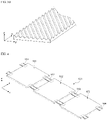
- projection of the recessed and projected structure on the first principal surface of the wiring member has a triangular prism shape as shown in FIG. 3A or a quadrangular pyramidal shape as shown in FIG. 3B . Since the triangular prism or the pyramid has a rectangular shape at the top of the projection, and is closely similar in visual impression to the quadrangular pyramidal recessed and projected structure on the light-receiving surface of the cell, the cell and the wiring member are unified in terms of a visual impression, so that the visuality of the module is improved.
- the arrangement of projections of the recessed and projected structure is not particularly limited.
- the shape of the projection is a triangular prism shape
- the extending direction of the triangular prism may be orthogonal to the extending direction (x direction) of the wiring member as shown in FIG. 3A , or the extending direction of the triangular prism may be parallel to the extending direction of the wiring member as shown in FIG. 3C .
- a triangular prism may extend in a direction which is not orthogonal or parallel to the extending direction of the wiring member, but forms a predetermined angle with the extending direction of the wiring member.
- the shape of the projections is a pyramidal shape
- the tops of the projections may be arranged in a square lattice shape as shown in FIG. 3B , or arranged zigzag.
- the height of the projection of the recessed and projected structure on the first principal surface of the wiring member is preferably about 0.1 to 500 ⁇ m.
- the height of the projections of the wiring member is 0.1 ⁇ m or more, there is a difference in visual impression between the wiring member and the smooth shape, and the cell surface and the wiring member can be made closely similar to each other in visual impression.
- the height of the projections on the wiring member is 500 ⁇ m or less, it is possible to form projections having a height equal to or less than the thickness of the wiring member, and the wiring member is not required to have an excessively large thickness. Thus, the flexibility and handling property of the wiring member can be maintained.
- the height of the recessed and projected structure of the wiring member is more preferably 0.5 to 20 ⁇ m.
- the projections on the wiring member are further closely similar in size to the projections on the cell, resulting in contribution to improvement of the visuality by making the projection shapes of the wiring member and the cell as similar to each other as possible.
- the method for forming a recessed and projected structure on the surface of the wiring member is not particularly limited.
- recessions and projections may be mechanically formed by a pressing method or the like, or recessions and projections may be chemically formed by wet etching.
- a recessed and projected structure with regularity is formed on the first principal surface of the wiring member.
- a recessed and projected structure with regularity can be formed on the surface of the wiring member by a mechanical method such as a method in which a recessed and projected shape of a roll surface is transferred to a base material surface.
- the first principal surface has a recessed and projected structure and equipped with electroconductive black layer not only at the exposed portions 821 and 831 on the light-receiving surface of the wiring members 82 and 83, but also at the connection portions 822, 823, 832 and 833 between the wiring members 82 and 83 and the cell. Since the black layer for preventing light reflection has electroconductivity, contact resistance between the electrode of the cell and the wiring member is small, so that an electric power loss can be reduced.
- the electroconductive black layer is disposed and a recessed and projected structure is formed on the entire first principal surface of the wiring member, patterning or the like is not needed, and therefore the wiring member can be manufactured at low cost.
- the productivity and the yield of the solar cell module can be improved.
- a solar cell string is first prepared by mutually connecting a plurality of cells through the wiring member.
- the electrode of the cell is connected to the wiring member through an electroconductive connection material such as solder, a conductive film or a conductive paste. Since the electroconductive connection member has metallic luster, the visuality of the module may be deteriorated when the electroconductive connection member is viewed from the outside. Thus, it is preferable that the electroconductive connection member is disposed only in a region which is not visible from the light-receiving surface of the module, and the electroconductive connection material is not disposed in a region visible from the light-receiving surface.
- electroconductive connection material in such a manner that the electroconductive connection material is not protruded from the region where the wiring member is disposed. Since the back side of the cell is not visible from the light-receiving surface of the module, there is no particular problem even if the electroconductive connection material is protruded from the region where the wiring member is disposed. However, since the portions 821 and 831 situated in gaps between adjacent cells are viewed from the light-receiving surface, it is preferable that the electroconductive connection material is not provided in this region.
- the solar cell string with a plurality of cells connected through the wiring member is sandwiched between a light-receiving-surface protection member 91 and a back-surface protection member 92 with an encapsulant 95 interposed between each of the protection members and the solar cell string, thereby forming the solar cell module.
- a laminate in which the light-receiving-side encapsulant, the solar cell string, the back-side encapsulant and the back-surface protection member are mounted in this order on the light-receiving-surface protection member is heated at predetermined conditions to cure the encapsulant.
- a transparent resin such as a polyethylene-based resin composition mainly composed of an olefin-based elastomer, polypropylene, an ethylene/ ⁇ -olefin copolymer, an ethylene/vinyl acetate copolymer (EVA), an ethylene/vinyl acetate/triallyl isocyanurate (EVAT), polyvinyl butyrate (PVB), silicon, urethane, acrylic or epoxy is used as the encapsulant 95.
- EVA ethylene/vinyl acetate copolymer
- EVAT ethylene/vinyl acetate/triallyl isocyanurate
- PVB polyvinyl butyrate
- silicon urethane
- acrylic or epoxy is used as the encapsulant 95.
- Materials of the encapsulants on the light-receiving side and the back side may be the same or different.
- the light-receiving-surface protection member 91 which is light-transmissive, glass, transparent plastic or the like is used.
- the back-surface protection member 92 may be any of light-transmissive, light-absorptive and light-reflective.
- a light-absorptive black sheet may be used as the back-surface protection member for unifying the colors of the cell and the wiring member to improve the visuality of the solar cell module.
- the black sheet for example, one including a black resin layer is used.
- the black resin layer has visible light-absorbency, and mainly absorbs visible light having a wavelength of 800 nm or less.
- the visible light transmittance of the black resin layer is preferably 10% or less.
- a resin composition containing a thermoplastic resin such as a polyolefin-based resin, a polyester-based resin, an acryl-based resin, a fluororesin or an ethylene-vinyl acetate resin and a colorant such as a pigment or a dye is preferably used.
- the back-surface protection member When a back-surface protection member including a black resin layer is used, the back-surface protection member is similar in appearance color to the cell, and therefore gaps between separately arranged cells are inconspicuous, so that a module having a high visuality is obtained.
- a wiring member having a predetermined shape is used, so that the metallic color of the wiring member is hardly visible because reflected light from the wiring member is not emitted outside from the light-receiving side of the module as described in detail later.
- a module is obtained which is uniformly colored black in its entirety, and has a high visuality.
- the entire surface can be uniformly colored black when the solar cell module is viewed from the light-receiving side.
- a recessed and projected structure is formed not only on the light-receiving surface of the solar cell, but also on the surface of the wiring member, the solar cell and the wiring member are unified in terms of a visual impression, and thus the wiring member becomes more difficult to view, so that a solar cell module having a high visuality is obtained.
- FIG. 2 shows a configuration in which the wiring member is disposed over substantially the total length in a cell connection direction
- the shape of the wiring member is not limited to the configuration shown in FIG. 2 .
- the electrodes of adjacent cells may be connected by band-shaped wiring members 181, 182 and 183 extending in a cell connection direction.
- the shape of the wiring member and the number of wiring members may be appropriately designed according to the electrode structure of the cells, etc.
- the wiring member used in the solar cell module of the present invention is used for interconnection of back contact solar cells.
- the above described wiring member can be used for interconnection of double-sided electrode type solar cells.
- the second principal surface of a wiring member 381 is connected to a light-receiving surface electrode of one cell 301 of two adjacent cells 301 and 302, and the first principal surface of a wiring member 381 is connected to a back electrode of the other cell 302 as shown in FIG. 5 .
- the wiring member is exposed to the light-receiving surface not only in a gap between adjacent cells but also at a connection portion of the cell with the light-receiving surface electrode.
- the electroconductive black layer is disposed on the entire surface of the wiring member, and recessed and projected structure is formed, and therefore even when any portion of the first principal surface of the wiring member is exposed to the light-receiving side, the wiring member is unified with the solar cell in terms of a visual impression, so that a module having a high visuality is obtained.
Landscapes
- Photovoltaic Devices (AREA)
Claims (9)
- Solarzellenmodul, umfassend:eine Solarzellenkette (120), in der mehrere Solarzellen (101, 102, 103), die jeweils eine Lichtempfangsfläche und eine Rückfläche aufweisen, durch ein Verdrahtungselement (82, 83) elektrisch verbunden sind;ein lichtdurchlässiges Lichtempfangsflächen-Schutzelement (91), das auf einer Lichtempfangsseite der Solarzellenkette angeordnet ist;ein Rückflächen-Schutzelement (92), das auf einer Rückseite der Solarzellenkette angeordnet ist; undein Verkapselungsmaterial (95), das zwischen dem Lichtempfangsflächen-Schutzelement und dem Rückflächen-Schutzelement angeordnet ist, um die Solarzellenkette zu verkapseln,wobeidie Solarzelle keine Metallelektrode auf der Lichtempfangsfläche aufweist und eine Metallelektrode nur auf der Rückfläche der Solarzelle angeordnet ist,das Verdrahtungselement eine erste Hauptoberfläche, eine zweite Hauptoberfläche und seitliche Flächen aufweist,die Metallelektrode auf der Rückfläche der Solarzelle mit der ersten Hauptoberfläche des Verdrahtungselements verbunden ist, dadurch gekennzeichnet, dassdie Lichtempfangsfläche der Solarzelle eine vertiefte und vorstehende Struktur aufweist, und die vertiefte und vorstehende Struktur auf der Lichtempfangsfläche der Solarzelle eine viereckige Pyramidenform aufweistdie gesamte erste Hauptoberfläche des Verdrahtungselements eine vertiefte und vorstehende Struktur aufweist, jeder der Vorsprünge der vertieften und vorstehenden Struktur auf der ersten Hauptoberfläche des Verdrahtungselements eine dreieckige Prismenform oder eine Pyramidenform aufweist, und die Vorsprünge regelmäßig angeordnet sind, undeine elektrisch leitende schwarze Schicht auf der gesamten ersten Hauptoberfläche des Verdrahtungselements angeordnet ist.
- Solarzellenmodul nach Anspruch 1, wobei ein Vorsprung der vertieften und vorstehenden Struktur auf der ersten Hauptoberfläche des Verdrahtungselements eine Höhe von 0,1 bis 500 µm aufweist.
- Solarzellenmodul nach Anspruch 1 oder 2, wobei die elektrisch leitende schwarze Schicht auch auf der seitlichen Fläche des Verdrahtungselements angeordnet ist.
- Solarzellenmodul nach einem der Ansprüche 1 bis 3, wobei ein Basismaterial des Verdrahtungselements Kupfer ist.
- Solarzellenmodul nach einem der Ansprüche 1 bis 4, wobei die elektrisch leitende schwarze Schicht eine plattierte Schicht ist, die auf einer Oberfläche eines Basismaterials des Verdrahtungselements ausgebildet ist.
- Solarzellenmodul nach einem der Ansprüche 1 bis 5, wobei die elektrisch leitende schwarze Schicht eine Metallschicht ist, die Palladium enthält.
- Solarzellenmodul nach einem der Ansprüche 1 bis 6, wobei ein elektrisch leitendes Verbindungsmaterial zum elektrischen Verbinden der Elektrode der Solarzelle mit dem Verdrahtungselement nicht in einem Bereich angeordnet ist, der von einer Lichtempfangsflächenseite sichtbar ist.
- Solarzellenmodul nach einem der Ansprüche 1 bis 7, wobei die auf der Rückfläche der Solarzelle angeordnete Metallelektrode und die erste Hauptoberfläche des Verdrahtungselements durch Lot miteinander verbunden sind.
- Solarzellenmodul nach einem der Ansprüche 1 bis 8, wobei das Rückflächen-Schutzelement ein schwarzes Blatt ist.
Applications Claiming Priority (2)
| Application Number | Priority Date | Filing Date | Title |
|---|---|---|---|
| JP2016182546 | 2016-09-20 | ||
| PCT/JP2017/023790 WO2018055863A1 (ja) | 2016-09-20 | 2017-06-28 | 太陽電池用配線材および太陽電池モジュール |
Publications (3)
| Publication Number | Publication Date |
|---|---|
| EP3518294A1 EP3518294A1 (de) | 2019-07-31 |
| EP3518294A4 EP3518294A4 (de) | 2020-03-18 |
| EP3518294B1 true EP3518294B1 (de) | 2022-06-15 |
Family
ID=61689506
Family Applications (1)
| Application Number | Title | Priority Date | Filing Date |
|---|---|---|---|
| EP17852644.8A Active EP3518294B1 (de) | 2016-09-20 | 2017-06-28 | Solarzellenmodul mit einem verdrahtungsleitungsmaterial zur verbindung von solarzellen |
Country Status (5)
| Country | Link |
|---|---|
| US (1) | US20190214518A1 (de) |
| EP (1) | EP3518294B1 (de) |
| JP (1) | JP6937762B2 (de) |
| CN (1) | CN109791956A (de) |
| WO (1) | WO2018055863A1 (de) |
Families Citing this family (3)
| Publication number | Priority date | Publication date | Assignee | Title |
|---|---|---|---|---|
| CN108909675B (zh) * | 2018-07-26 | 2021-08-24 | 京东方科技集团股份有限公司 | 一种玻璃及控制方法 |
| CN109065656A (zh) * | 2018-10-31 | 2018-12-21 | 伟创力有限公司 | 形成用于集成在太阳能电池组件中的有色导电焊带的方法 |
| JP2021059697A (ja) * | 2019-10-09 | 2021-04-15 | 日東電工株式会社 | フッ素樹脂シート及び粘着テープ |
Family Cites Families (12)
| Publication number | Priority date | Publication date | Assignee | Title |
|---|---|---|---|---|
| JP2859829B2 (ja) * | 1995-05-18 | 1999-02-24 | 株式会社富士電機総合研究所 | 太陽光発電用屋根材 |
| JPH1093125A (ja) | 1996-09-13 | 1998-04-10 | Sanyo Electric Co Ltd | 太陽電池モジュール |
| JPH10313126A (ja) * | 1997-05-13 | 1998-11-24 | Sharp Corp | 太陽電池素子及びその電極の表面処理方法及び太陽電池モジュール |
| US20070125415A1 (en) * | 2005-12-05 | 2007-06-07 | Massachusetts Institute Of Technology | Light capture with patterned solar cell bus wires |
| JP4780008B2 (ja) * | 2006-12-14 | 2011-09-28 | 日立電線株式会社 | 太陽電池用めっき線及びその製造方法 |
| US20100294329A1 (en) * | 2007-09-26 | 2010-11-25 | Hitachi Chemical Company, Ltd. | Member for conductor connection, method for manufacturing the same, connection structure, and solar cell module |
| KR101130197B1 (ko) * | 2009-09-28 | 2012-03-30 | 엘지전자 주식회사 | 태양전지 모듈 및 그 제조 방법 |
| JP5842170B2 (ja) * | 2011-06-23 | 2016-01-13 | パナソニックIpマネジメント株式会社 | 太陽電池モジュール |
| JP2013033848A (ja) * | 2011-08-02 | 2013-02-14 | Jx Nippon Oil & Energy Corp | 太陽電池モジュール及びその製造方法 |
| WO2013161030A1 (ja) * | 2012-04-26 | 2013-10-31 | 三洋電機株式会社 | 太陽電池モジュール及び太陽電池モジュールの製造方法 |
| KR102124520B1 (ko) * | 2013-10-29 | 2020-06-18 | 엘지전자 주식회사 | 태양 전지 모듈 및 그 제조 방법 |
| JP2015222763A (ja) * | 2014-05-22 | 2015-12-10 | 帝人デュポンフィルム株式会社 | 太陽電池用黒色ポリエステルフィルム |
-
2017
- 2017-06-28 CN CN201780057262.3A patent/CN109791956A/zh active Pending
- 2017-06-28 JP JP2018540644A patent/JP6937762B2/ja active Active
- 2017-06-28 WO PCT/JP2017/023790 patent/WO2018055863A1/ja not_active Ceased
- 2017-06-28 EP EP17852644.8A patent/EP3518294B1/de active Active
- 2017-06-28 US US16/335,119 patent/US20190214518A1/en not_active Abandoned
Also Published As
| Publication number | Publication date |
|---|---|
| JP6937762B2 (ja) | 2021-09-22 |
| JPWO2018055863A1 (ja) | 2019-07-04 |
| EP3518294A1 (de) | 2019-07-31 |
| CN109791956A (zh) | 2019-05-21 |
| WO2018055863A1 (ja) | 2018-03-29 |
| EP3518294A4 (de) | 2020-03-18 |
| US20190214518A1 (en) | 2019-07-11 |
Similar Documents
| Publication | Publication Date | Title |
|---|---|---|
| CN111615752B (zh) | 太阳能电池模块 | |
| JP5410050B2 (ja) | 太陽電池モジュール | |
| EP3522237B1 (de) | Solarzellenmodul | |
| CN100505280C (zh) | 用临时衬底制造太阳能电池薄片的方法和太阳能电池单元 | |
| TWI495124B (zh) | 太陽能電池及太陽能電池模組 | |
| KR101258968B1 (ko) | 태양 전지 및 태양 전지의 제조 방법 | |
| EP2469604A1 (de) | Solarbatterie, solarbatteriemodul und solarbatteriesystem | |
| KR20140003691A (ko) | 태양 전지 모듈 및 이에 적용되는 리본 결합체 | |
| EP3128560B1 (de) | Band für ein solarzellenpanel, verfahren zu dessen herstellung und solarzellenpanel | |
| CN114207843B (zh) | 太阳能电池单元的制造方法、太阳能电池单元、太阳能电池装置和太阳能电池模块 | |
| EP3553832B1 (de) | Solarzellenmodul | |
| EP2418689B1 (de) | Solarzellenplatte | |
| JPWO2016158299A1 (ja) | 太陽電池およびその製造方法、太陽電池モジュール、ならびに配線シート | |
| JP2008010857A (ja) | 太陽電池モジュール | |
| EP3518294A1 (de) | Verdrahtungsleitungsmaterial für solarzellen und solarzellenmodul | |
| KR101146734B1 (ko) | 태양 전지 셀 및 이를 구비한 태양 전지 모듈 | |
| KR20140095658A (ko) | 태양 전지 | |
| US11063160B2 (en) | Solar cell module | |
| KR101192345B1 (ko) | 태양전지의 전극 패턴 및 이를 포함하는 태양전지 | |
| JP5988154B2 (ja) | 車載用太陽電池モジュール | |
| US20170092789A1 (en) | Solar cell module | |
| JP2022006836A (ja) | 太陽電池ストリング及び太陽電池モジュール | |
| KR20160041649A (ko) | 태양 전지용 리본 및 이를 포함하는 태양 전지 모듈 | |
| US20170092797A1 (en) | Solar cell module | |
| JP2018195653A (ja) | 太陽電池モジュール |
Legal Events
| Date | Code | Title | Description |
|---|---|---|---|
| STAA | Information on the status of an ep patent application or granted ep patent |
Free format text: STATUS: THE INTERNATIONAL PUBLICATION HAS BEEN MADE |
|
| PUAI | Public reference made under article 153(3) epc to a published international application that has entered the european phase |
Free format text: ORIGINAL CODE: 0009012 |
|
| STAA | Information on the status of an ep patent application or granted ep patent |
Free format text: STATUS: REQUEST FOR EXAMINATION WAS MADE |
|
| 17P | Request for examination filed |
Effective date: 20190409 |
|
| AK | Designated contracting states |
Kind code of ref document: A1 Designated state(s): AL AT BE BG CH CY CZ DE DK EE ES FI FR GB GR HR HU IE IS IT LI LT LU LV MC MK MT NL NO PL PT RO RS SE SI SK SM TR |
|
| AX | Request for extension of the european patent |
Extension state: BA ME |
|
| DAV | Request for validation of the european patent (deleted) | ||
| DAX | Request for extension of the european patent (deleted) | ||
| A4 | Supplementary search report drawn up and despatched |
Effective date: 20200219 |
|
| RIC1 | Information provided on ipc code assigned before grant |
Ipc: H01L 31/05 20140101AFI20200213BHEP |
|
| RIC1 | Information provided on ipc code assigned before grant |
Ipc: H01L 31/0236 20060101ALI20210916BHEP Ipc: H01L 31/05 20140101AFI20210916BHEP |
|
| GRAP | Despatch of communication of intention to grant a patent |
Free format text: ORIGINAL CODE: EPIDOSNIGR1 |
|
| STAA | Information on the status of an ep patent application or granted ep patent |
Free format text: STATUS: GRANT OF PATENT IS INTENDED |
|
| INTG | Intention to grant announced |
Effective date: 20220104 |
|
| GRAS | Grant fee paid |
Free format text: ORIGINAL CODE: EPIDOSNIGR3 |
|
| GRAA | (expected) grant |
Free format text: ORIGINAL CODE: 0009210 |
|
| STAA | Information on the status of an ep patent application or granted ep patent |
Free format text: STATUS: THE PATENT HAS BEEN GRANTED |
|
| AK | Designated contracting states |
Kind code of ref document: B1 Designated state(s): AL AT BE BG CH CY CZ DE DK EE ES FI FR GB GR HR HU IE IS IT LI LT LU LV MC MK MT NL NO PL PT RO RS SE SI SK SM TR |
|
| REG | Reference to a national code |
Ref country code: CH Ref legal event code: EP Ref country code: GB Ref legal event code: FG4D |
|
| REG | Reference to a national code |
Ref country code: IE Ref legal event code: FG4D |
|
| REG | Reference to a national code |
Ref country code: DE Ref legal event code: R096 Ref document number: 602017058619 Country of ref document: DE |
|
| REG | Reference to a national code |
Ref country code: AT Ref legal event code: REF Ref document number: 1498908 Country of ref document: AT Kind code of ref document: T Effective date: 20220715 |
|
| REG | Reference to a national code |
Ref country code: LT Ref legal event code: MG9D |
|
| REG | Reference to a national code |
Ref country code: NL Ref legal event code: MP Effective date: 20220615 |
|
| PG25 | Lapsed in a contracting state [announced via postgrant information from national office to epo] |
Ref country code: SE Free format text: LAPSE BECAUSE OF FAILURE TO SUBMIT A TRANSLATION OF THE DESCRIPTION OR TO PAY THE FEE WITHIN THE PRESCRIBED TIME-LIMIT Effective date: 20220615 Ref country code: NO Free format text: LAPSE BECAUSE OF FAILURE TO SUBMIT A TRANSLATION OF THE DESCRIPTION OR TO PAY THE FEE WITHIN THE PRESCRIBED TIME-LIMIT Effective date: 20220915 Ref country code: LT Free format text: LAPSE BECAUSE OF FAILURE TO SUBMIT A TRANSLATION OF THE DESCRIPTION OR TO PAY THE FEE WITHIN THE PRESCRIBED TIME-LIMIT Effective date: 20220615 Ref country code: HR Free format text: LAPSE BECAUSE OF FAILURE TO SUBMIT A TRANSLATION OF THE DESCRIPTION OR TO PAY THE FEE WITHIN THE PRESCRIBED TIME-LIMIT Effective date: 20220615 Ref country code: GR Free format text: LAPSE BECAUSE OF FAILURE TO SUBMIT A TRANSLATION OF THE DESCRIPTION OR TO PAY THE FEE WITHIN THE PRESCRIBED TIME-LIMIT Effective date: 20220916 Ref country code: FI Free format text: LAPSE BECAUSE OF FAILURE TO SUBMIT A TRANSLATION OF THE DESCRIPTION OR TO PAY THE FEE WITHIN THE PRESCRIBED TIME-LIMIT Effective date: 20220615 Ref country code: BG Free format text: LAPSE BECAUSE OF FAILURE TO SUBMIT A TRANSLATION OF THE DESCRIPTION OR TO PAY THE FEE WITHIN THE PRESCRIBED TIME-LIMIT Effective date: 20220915 |
|
| REG | Reference to a national code |
Ref country code: AT Ref legal event code: MK05 Ref document number: 1498908 Country of ref document: AT Kind code of ref document: T Effective date: 20220615 |
|
| PG25 | Lapsed in a contracting state [announced via postgrant information from national office to epo] |
Ref country code: RS Free format text: LAPSE BECAUSE OF FAILURE TO SUBMIT A TRANSLATION OF THE DESCRIPTION OR TO PAY THE FEE WITHIN THE PRESCRIBED TIME-LIMIT Effective date: 20220615 Ref country code: LV Free format text: LAPSE BECAUSE OF FAILURE TO SUBMIT A TRANSLATION OF THE DESCRIPTION OR TO PAY THE FEE WITHIN THE PRESCRIBED TIME-LIMIT Effective date: 20220615 |
|
| PG25 | Lapsed in a contracting state [announced via postgrant information from national office to epo] |
Ref country code: NL Free format text: LAPSE BECAUSE OF FAILURE TO SUBMIT A TRANSLATION OF THE DESCRIPTION OR TO PAY THE FEE WITHIN THE PRESCRIBED TIME-LIMIT Effective date: 20220615 |
|
| PG25 | Lapsed in a contracting state [announced via postgrant information from national office to epo] |
Ref country code: SM Free format text: LAPSE BECAUSE OF FAILURE TO SUBMIT A TRANSLATION OF THE DESCRIPTION OR TO PAY THE FEE WITHIN THE PRESCRIBED TIME-LIMIT Effective date: 20220615 Ref country code: SK Free format text: LAPSE BECAUSE OF FAILURE TO SUBMIT A TRANSLATION OF THE DESCRIPTION OR TO PAY THE FEE WITHIN THE PRESCRIBED TIME-LIMIT Effective date: 20220615 Ref country code: RO Free format text: LAPSE BECAUSE OF FAILURE TO SUBMIT A TRANSLATION OF THE DESCRIPTION OR TO PAY THE FEE WITHIN THE PRESCRIBED TIME-LIMIT Effective date: 20220615 Ref country code: PT Free format text: LAPSE BECAUSE OF FAILURE TO SUBMIT A TRANSLATION OF THE DESCRIPTION OR TO PAY THE FEE WITHIN THE PRESCRIBED TIME-LIMIT Effective date: 20221017 Ref country code: ES Free format text: LAPSE BECAUSE OF FAILURE TO SUBMIT A TRANSLATION OF THE DESCRIPTION OR TO PAY THE FEE WITHIN THE PRESCRIBED TIME-LIMIT Effective date: 20220615 Ref country code: EE Free format text: LAPSE BECAUSE OF FAILURE TO SUBMIT A TRANSLATION OF THE DESCRIPTION OR TO PAY THE FEE WITHIN THE PRESCRIBED TIME-LIMIT Effective date: 20220615 Ref country code: CZ Free format text: LAPSE BECAUSE OF FAILURE TO SUBMIT A TRANSLATION OF THE DESCRIPTION OR TO PAY THE FEE WITHIN THE PRESCRIBED TIME-LIMIT Effective date: 20220615 Ref country code: AT Free format text: LAPSE BECAUSE OF FAILURE TO SUBMIT A TRANSLATION OF THE DESCRIPTION OR TO PAY THE FEE WITHIN THE PRESCRIBED TIME-LIMIT Effective date: 20220615 |
|
| REG | Reference to a national code |
Ref country code: CH Ref legal event code: PL |
|
| REG | Reference to a national code |
Ref country code: BE Ref legal event code: MM Effective date: 20220630 |
|
| PG25 | Lapsed in a contracting state [announced via postgrant information from national office to epo] |
Ref country code: PL Free format text: LAPSE BECAUSE OF FAILURE TO SUBMIT A TRANSLATION OF THE DESCRIPTION OR TO PAY THE FEE WITHIN THE PRESCRIBED TIME-LIMIT Effective date: 20220615 Ref country code: IS Free format text: LAPSE BECAUSE OF FAILURE TO SUBMIT A TRANSLATION OF THE DESCRIPTION OR TO PAY THE FEE WITHIN THE PRESCRIBED TIME-LIMIT Effective date: 20221015 |
|
| REG | Reference to a national code |
Ref country code: DE Ref legal event code: R097 Ref document number: 602017058619 Country of ref document: DE |
|
| PG25 | Lapsed in a contracting state [announced via postgrant information from national office to epo] |
Ref country code: MC Free format text: LAPSE BECAUSE OF FAILURE TO SUBMIT A TRANSLATION OF THE DESCRIPTION OR TO PAY THE FEE WITHIN THE PRESCRIBED TIME-LIMIT Effective date: 20220615 Ref country code: AL Free format text: LAPSE BECAUSE OF FAILURE TO SUBMIT A TRANSLATION OF THE DESCRIPTION OR TO PAY THE FEE WITHIN THE PRESCRIBED TIME-LIMIT Effective date: 20220615 |
|
| PLBE | No opposition filed within time limit |
Free format text: ORIGINAL CODE: 0009261 |
|
| STAA | Information on the status of an ep patent application or granted ep patent |
Free format text: STATUS: NO OPPOSITION FILED WITHIN TIME LIMIT |
|
| PG25 | Lapsed in a contracting state [announced via postgrant information from national office to epo] |
Ref country code: LU Free format text: LAPSE BECAUSE OF NON-PAYMENT OF DUE FEES Effective date: 20220628 Ref country code: LI Free format text: LAPSE BECAUSE OF NON-PAYMENT OF DUE FEES Effective date: 20220630 Ref country code: IE Free format text: LAPSE BECAUSE OF NON-PAYMENT OF DUE FEES Effective date: 20220628 Ref country code: DK Free format text: LAPSE BECAUSE OF FAILURE TO SUBMIT A TRANSLATION OF THE DESCRIPTION OR TO PAY THE FEE WITHIN THE PRESCRIBED TIME-LIMIT Effective date: 20220615 Ref country code: CH Free format text: LAPSE BECAUSE OF NON-PAYMENT OF DUE FEES Effective date: 20220630 |
|
| 26N | No opposition filed |
Effective date: 20230316 |
|
| GBPC | Gb: european patent ceased through non-payment of renewal fee |
Effective date: 20220915 |
|
| PG25 | Lapsed in a contracting state [announced via postgrant information from national office to epo] |
Ref country code: SI Free format text: LAPSE BECAUSE OF FAILURE TO SUBMIT A TRANSLATION OF THE DESCRIPTION OR TO PAY THE FEE WITHIN THE PRESCRIBED TIME-LIMIT Effective date: 20220615 Ref country code: BE Free format text: LAPSE BECAUSE OF NON-PAYMENT OF DUE FEES Effective date: 20220630 |
|
| PG25 | Lapsed in a contracting state [announced via postgrant information from national office to epo] |
Ref country code: FR Free format text: LAPSE BECAUSE OF NON-PAYMENT OF DUE FEES Effective date: 20220815 |
|
| PG25 | Lapsed in a contracting state [announced via postgrant information from national office to epo] |
Ref country code: GB Free format text: LAPSE BECAUSE OF NON-PAYMENT OF DUE FEES Effective date: 20220915 |
|
| PG25 | Lapsed in a contracting state [announced via postgrant information from national office to epo] |
Ref country code: IT Free format text: LAPSE BECAUSE OF FAILURE TO SUBMIT A TRANSLATION OF THE DESCRIPTION OR TO PAY THE FEE WITHIN THE PRESCRIBED TIME-LIMIT Effective date: 20220615 |
|
| PG25 | Lapsed in a contracting state [announced via postgrant information from national office to epo] |
Ref country code: HU Free format text: LAPSE BECAUSE OF FAILURE TO SUBMIT A TRANSLATION OF THE DESCRIPTION OR TO PAY THE FEE WITHIN THE PRESCRIBED TIME-LIMIT; INVALID AB INITIO Effective date: 20170628 |
|
| PG25 | Lapsed in a contracting state [announced via postgrant information from national office to epo] |
Ref country code: MK Free format text: LAPSE BECAUSE OF FAILURE TO SUBMIT A TRANSLATION OF THE DESCRIPTION OR TO PAY THE FEE WITHIN THE PRESCRIBED TIME-LIMIT Effective date: 20220615 Ref country code: CY Free format text: LAPSE BECAUSE OF FAILURE TO SUBMIT A TRANSLATION OF THE DESCRIPTION OR TO PAY THE FEE WITHIN THE PRESCRIBED TIME-LIMIT Effective date: 20220615 |
|
| PG25 | Lapsed in a contracting state [announced via postgrant information from national office to epo] |
Ref country code: TR Free format text: LAPSE BECAUSE OF FAILURE TO SUBMIT A TRANSLATION OF THE DESCRIPTION OR TO PAY THE FEE WITHIN THE PRESCRIBED TIME-LIMIT Effective date: 20220615 |
|
| PG25 | Lapsed in a contracting state [announced via postgrant information from national office to epo] |
Ref country code: MT Free format text: LAPSE BECAUSE OF FAILURE TO SUBMIT A TRANSLATION OF THE DESCRIPTION OR TO PAY THE FEE WITHIN THE PRESCRIBED TIME-LIMIT Effective date: 20220615 |
|
| PG25 | Lapsed in a contracting state [announced via postgrant information from national office to epo] |
Ref country code: BG Free format text: LAPSE BECAUSE OF FAILURE TO SUBMIT A TRANSLATION OF THE DESCRIPTION OR TO PAY THE FEE WITHIN THE PRESCRIBED TIME-LIMIT Effective date: 20220615 |
|
| REG | Reference to a national code |
Ref country code: DE Ref legal event code: R079 Ref document number: 602017058619 Country of ref document: DE Free format text: PREVIOUS MAIN CLASS: H01L0031050000 Ipc: H10F0019900000 |
|
| PG25 | Lapsed in a contracting state [announced via postgrant information from national office to epo] |
Ref country code: BG Free format text: LAPSE BECAUSE OF FAILURE TO SUBMIT A TRANSLATION OF THE DESCRIPTION OR TO PAY THE FEE WITHIN THE PRESCRIBED TIME-LIMIT Effective date: 20220615 |
|
| PGFP | Annual fee paid to national office [announced via postgrant information from national office to epo] |
Ref country code: DE Payment date: 20250507 Year of fee payment: 9 |