EP3506499A2 - Tunable resonator element, filter circuit and method - Google Patents
Tunable resonator element, filter circuit and method Download PDFInfo
- Publication number
- EP3506499A2 EP3506499A2 EP18210383.8A EP18210383A EP3506499A2 EP 3506499 A2 EP3506499 A2 EP 3506499A2 EP 18210383 A EP18210383 A EP 18210383A EP 3506499 A2 EP3506499 A2 EP 3506499A2
- Authority
- EP
- European Patent Office
- Prior art keywords
- resonator
- filter
- tuning
- resonators
- coupled
- Prior art date
- Legal status (The legal status is an assumption and is not a legal conclusion. Google has not performed a legal analysis and makes no representation as to the accuracy of the status listed.)
- Granted
Links
- 238000000034 method Methods 0.000 title claims description 26
- 239000003990 capacitor Substances 0.000 claims abstract description 44
- 230000008878 coupling Effects 0.000 claims description 62
- 238000010168 coupling process Methods 0.000 claims description 62
- 238000005859 coupling reaction Methods 0.000 claims description 62
- 239000000758 substrate Substances 0.000 claims description 25
- 229910052751 metal Inorganic materials 0.000 claims description 22
- 239000002184 metal Substances 0.000 claims description 22
- 230000008569 process Effects 0.000 claims description 14
- 238000010348 incorporation Methods 0.000 abstract 1
- 239000000463 material Substances 0.000 description 40
- 238000004891 communication Methods 0.000 description 15
- 238000010586 diagram Methods 0.000 description 14
- PMHQVHHXPFUNSP-UHFFFAOYSA-M copper(1+);methylsulfanylmethane;bromide Chemical compound Br[Cu].CSC PMHQVHHXPFUNSP-UHFFFAOYSA-M 0.000 description 11
- 230000003071 parasitic effect Effects 0.000 description 8
- 230000003068 static effect Effects 0.000 description 7
- 238000001465 metallisation Methods 0.000 description 6
- 238000004088 simulation Methods 0.000 description 6
- 238000004519 manufacturing process Methods 0.000 description 5
- 238000010276 construction Methods 0.000 description 4
- 239000013078 crystal Substances 0.000 description 4
- 239000003989 dielectric material Substances 0.000 description 4
- 238000013459 approach Methods 0.000 description 3
- 238000005516 engineering process Methods 0.000 description 3
- 230000001965 increasing effect Effects 0.000 description 3
- 230000001939 inductive effect Effects 0.000 description 3
- 238000002955 isolation Methods 0.000 description 3
- GQYHUHYESMUTHG-UHFFFAOYSA-N lithium niobate Chemical compound [Li+].[O-][Nb](=O)=O GQYHUHYESMUTHG-UHFFFAOYSA-N 0.000 description 3
- 230000010287 polarization Effects 0.000 description 3
- 238000010897 surface acoustic wave method Methods 0.000 description 3
- RYGMFSIKBFXOCR-UHFFFAOYSA-N Copper Chemical compound [Cu] RYGMFSIKBFXOCR-UHFFFAOYSA-N 0.000 description 2
- 229910003327 LiNbO3 Inorganic materials 0.000 description 2
- VYPSYNLAJGMNEJ-UHFFFAOYSA-N Silicium dioxide Chemical compound O=[Si]=O VYPSYNLAJGMNEJ-UHFFFAOYSA-N 0.000 description 2
- XAGFODPZIPBFFR-UHFFFAOYSA-N aluminium Chemical compound [Al] XAGFODPZIPBFFR-UHFFFAOYSA-N 0.000 description 2
- 230000008901 benefit Effects 0.000 description 2
- 239000002131 composite material Substances 0.000 description 2
- 229910052802 copper Inorganic materials 0.000 description 2
- 239000010949 copper Substances 0.000 description 2
- 238000013461 design Methods 0.000 description 2
- 239000002019 doping agent Substances 0.000 description 2
- 238000003780 insertion Methods 0.000 description 2
- 230000037431 insertion Effects 0.000 description 2
- 239000012528 membrane Substances 0.000 description 2
- 238000012986 modification Methods 0.000 description 2
- 230000004048 modification Effects 0.000 description 2
- UKDIAJWKFXFVFG-UHFFFAOYSA-N potassium;oxido(dioxo)niobium Chemical compound [K+].[O-][Nb](=O)=O UKDIAJWKFXFVFG-UHFFFAOYSA-N 0.000 description 2
- 229910052706 scandium Inorganic materials 0.000 description 2
- SIXSYDAISGFNSX-UHFFFAOYSA-N scandium atom Chemical compound [Sc] SIXSYDAISGFNSX-UHFFFAOYSA-N 0.000 description 2
- WSMQKESQZFQMFW-UHFFFAOYSA-N 5-methyl-pyrazole-3-carboxylic acid Chemical compound CC1=CC(C(O)=O)=NN1 WSMQKESQZFQMFW-UHFFFAOYSA-N 0.000 description 1
- PIGFYZPCRLYGLF-UHFFFAOYSA-N Aluminum nitride Chemical compound [Al]#N PIGFYZPCRLYGLF-UHFFFAOYSA-N 0.000 description 1
- 229910003334 KNbO3 Inorganic materials 0.000 description 1
- XUIMIQQOPSSXEZ-UHFFFAOYSA-N Silicon Chemical compound [Si] XUIMIQQOPSSXEZ-UHFFFAOYSA-N 0.000 description 1
- 230000002411 adverse Effects 0.000 description 1
- 230000002776 aggregation Effects 0.000 description 1
- 238000004220 aggregation Methods 0.000 description 1
- 229910052782 aluminium Inorganic materials 0.000 description 1
- LUKDNTKUBVKBMZ-UHFFFAOYSA-N aluminum scandium Chemical compound [Al].[Sc] LUKDNTKUBVKBMZ-UHFFFAOYSA-N 0.000 description 1
- 230000008859 change Effects 0.000 description 1
- 230000001419 dependent effect Effects 0.000 description 1
- 238000000151 deposition Methods 0.000 description 1
- 230000008021 deposition Effects 0.000 description 1
- 230000000694 effects Effects 0.000 description 1
- 239000013013 elastic material Substances 0.000 description 1
- 230000005684 electric field Effects 0.000 description 1
- 238000005530 etching Methods 0.000 description 1
- 238000001914 filtration Methods 0.000 description 1
- 230000006872 improvement Effects 0.000 description 1
- 229910052738 indium Inorganic materials 0.000 description 1
- 239000011810 insulating material Substances 0.000 description 1
- 238000001459 lithography Methods 0.000 description 1
- 230000007774 longterm Effects 0.000 description 1
- 238000010295 mobile communication Methods 0.000 description 1
- 238000013021 overheating Methods 0.000 description 1
- 238000012545 processing Methods 0.000 description 1
- 230000000644 propagated effect Effects 0.000 description 1
- 238000005546 reactive sputtering Methods 0.000 description 1
- 238000000926 separation method Methods 0.000 description 1
- 229910052710 silicon Inorganic materials 0.000 description 1
- 239000010703 silicon Substances 0.000 description 1
- 235000012239 silicon dioxide Nutrition 0.000 description 1
- 239000000377 silicon dioxide Substances 0.000 description 1
- WFKWXMTUELFFGS-UHFFFAOYSA-N tungsten Chemical compound [W] WFKWXMTUELFFGS-UHFFFAOYSA-N 0.000 description 1
Images


Classifications
-
- H—ELECTRICITY
- H03—ELECTRONIC CIRCUITRY
- H03H—IMPEDANCE NETWORKS, e.g. RESONANT CIRCUITS; RESONATORS
- H03H9/00—Networks comprising electromechanical or electro-acoustic devices; Electromechanical resonators
- H03H9/46—Filters
- H03H9/54—Filters comprising resonators of piezo-electric or electrostrictive material
- H03H9/547—Notch filters, e.g. notch BAW or thin film resonator filters
-
- H—ELECTRICITY
- H03—ELECTRONIC CIRCUITRY
- H03F—AMPLIFIERS
- H03F3/00—Amplifiers with only discharge tubes or only semiconductor devices as amplifying elements
- H03F3/189—High frequency amplifiers, e.g. radio frequency amplifiers
- H03F3/19—High frequency amplifiers, e.g. radio frequency amplifiers with semiconductor devices only
- H03F3/195—High frequency amplifiers, e.g. radio frequency amplifiers with semiconductor devices only in integrated circuits
-
- H—ELECTRICITY
- H03—ELECTRONIC CIRCUITRY
- H03F—AMPLIFIERS
- H03F3/00—Amplifiers with only discharge tubes or only semiconductor devices as amplifying elements
- H03F3/20—Power amplifiers, e.g. Class B amplifiers, Class C amplifiers
- H03F3/21—Power amplifiers, e.g. Class B amplifiers, Class C amplifiers with semiconductor devices only
-
- H—ELECTRICITY
- H03—ELECTRONIC CIRCUITRY
- H03H—IMPEDANCE NETWORKS, e.g. RESONANT CIRCUITS; RESONATORS
- H03H11/00—Networks using active elements
- H03H11/02—Multiple-port networks
- H03H11/04—Frequency selective two-port networks
- H03H11/12—Frequency selective two-port networks using amplifiers with feedback
- H03H11/1291—Current or voltage controlled filters
-
- H—ELECTRICITY
- H03—ELECTRONIC CIRCUITRY
- H03H—IMPEDANCE NETWORKS, e.g. RESONANT CIRCUITS; RESONATORS
- H03H3/00—Apparatus or processes specially adapted for the manufacture of impedance networks, resonating circuits, resonators
- H03H3/007—Apparatus or processes specially adapted for the manufacture of impedance networks, resonating circuits, resonators for the manufacture of electromechanical resonators or networks
- H03H3/02—Apparatus or processes specially adapted for the manufacture of impedance networks, resonating circuits, resonators for the manufacture of electromechanical resonators or networks for the manufacture of piezoelectric or electrostrictive resonators or networks
-
- H—ELECTRICITY
- H03—ELECTRONIC CIRCUITRY
- H03H—IMPEDANCE NETWORKS, e.g. RESONANT CIRCUITS; RESONATORS
- H03H7/00—Multiple-port networks comprising only passive electrical elements as network components
- H03H7/01—Frequency selective two-port networks
- H03H7/0115—Frequency selective two-port networks comprising only inductors and capacitors
-
- H—ELECTRICITY
- H03—ELECTRONIC CIRCUITRY
- H03H—IMPEDANCE NETWORKS, e.g. RESONANT CIRCUITS; RESONATORS
- H03H7/00—Multiple-port networks comprising only passive electrical elements as network components
- H03H7/01—Frequency selective two-port networks
- H03H7/0153—Electrical filters; Controlling thereof
- H03H7/0161—Bandpass filters
-
- H—ELECTRICITY
- H03—ELECTRONIC CIRCUITRY
- H03H—IMPEDANCE NETWORKS, e.g. RESONANT CIRCUITS; RESONATORS
- H03H7/00—Multiple-port networks comprising only passive electrical elements as network components
- H03H7/01—Frequency selective two-port networks
- H03H7/12—Bandpass or bandstop filters with adjustable bandwidth and fixed centre frequency
-
- H—ELECTRICITY
- H03—ELECTRONIC CIRCUITRY
- H03H—IMPEDANCE NETWORKS, e.g. RESONANT CIRCUITS; RESONATORS
- H03H7/00—Multiple-port networks comprising only passive electrical elements as network components
- H03H7/01—Frequency selective two-port networks
- H03H7/17—Structural details of sub-circuits of frequency selective networks
- H03H7/1741—Comprising typical LC combinations, irrespective of presence and location of additional resistors
-
- H—ELECTRICITY
- H03—ELECTRONIC CIRCUITRY
- H03H—IMPEDANCE NETWORKS, e.g. RESONANT CIRCUITS; RESONATORS
- H03H7/00—Multiple-port networks comprising only passive electrical elements as network components
- H03H7/46—Networks for connecting several sources or loads, working on different frequencies or frequency bands, to a common load or source
- H03H7/463—Duplexers
-
- H—ELECTRICITY
- H03—ELECTRONIC CIRCUITRY
- H03H—IMPEDANCE NETWORKS, e.g. RESONANT CIRCUITS; RESONATORS
- H03H9/00—Networks comprising electromechanical or electro-acoustic devices; Electromechanical resonators
- H03H9/0004—Impedance-matching networks
-
- H—ELECTRICITY
- H03—ELECTRONIC CIRCUITRY
- H03H—IMPEDANCE NETWORKS, e.g. RESONANT CIRCUITS; RESONATORS
- H03H9/00—Networks comprising electromechanical or electro-acoustic devices; Electromechanical resonators
- H03H9/02—Details
- H03H9/02007—Details of bulk acoustic wave devices
-
- H—ELECTRICITY
- H03—ELECTRONIC CIRCUITRY
- H03H—IMPEDANCE NETWORKS, e.g. RESONANT CIRCUITS; RESONATORS
- H03H9/00—Networks comprising electromechanical or electro-acoustic devices; Electromechanical resonators
- H03H9/02—Details
- H03H9/02007—Details of bulk acoustic wave devices
- H03H9/02015—Characteristics of piezoelectric layers, e.g. cutting angles
- H03H9/02031—Characteristics of piezoelectric layers, e.g. cutting angles consisting of ceramic
-
- H—ELECTRICITY
- H03—ELECTRONIC CIRCUITRY
- H03H—IMPEDANCE NETWORKS, e.g. RESONANT CIRCUITS; RESONATORS
- H03H9/00—Networks comprising electromechanical or electro-acoustic devices; Electromechanical resonators
- H03H9/02—Details
- H03H9/05—Holders; Supports
- H03H9/0538—Constructional combinations of supports or holders with electromechanical or other electronic elements
- H03H9/0547—Constructional combinations of supports or holders with electromechanical or other electronic elements consisting of a vertical arrangement
-
- H—ELECTRICITY
- H03—ELECTRONIC CIRCUITRY
- H03H—IMPEDANCE NETWORKS, e.g. RESONANT CIRCUITS; RESONATORS
- H03H9/00—Networks comprising electromechanical or electro-acoustic devices; Electromechanical resonators
- H03H9/02—Details
- H03H9/125—Driving means, e.g. electrodes, coils
- H03H9/13—Driving means, e.g. electrodes, coils for networks consisting of piezoelectric or electrostrictive materials
- H03H9/131—Driving means, e.g. electrodes, coils for networks consisting of piezoelectric or electrostrictive materials consisting of a multilayered structure
-
- H—ELECTRICITY
- H03—ELECTRONIC CIRCUITRY
- H03H—IMPEDANCE NETWORKS, e.g. RESONANT CIRCUITS; RESONATORS
- H03H9/00—Networks comprising electromechanical or electro-acoustic devices; Electromechanical resonators
- H03H9/15—Constructional features of resonators consisting of piezoelectric or electrostrictive material
- H03H9/17—Constructional features of resonators consisting of piezoelectric or electrostrictive material having a single resonator
- H03H9/171—Constructional features of resonators consisting of piezoelectric or electrostrictive material having a single resonator implemented with thin-film techniques, i.e. of the film bulk acoustic resonator [FBAR] type
- H03H9/172—Means for mounting on a substrate, i.e. means constituting the material interface confining the waves to a volume
- H03H9/175—Acoustic mirrors
-
- H—ELECTRICITY
- H03—ELECTRONIC CIRCUITRY
- H03H—IMPEDANCE NETWORKS, e.g. RESONANT CIRCUITS; RESONATORS
- H03H9/00—Networks comprising electromechanical or electro-acoustic devices; Electromechanical resonators
- H03H9/15—Constructional features of resonators consisting of piezoelectric or electrostrictive material
- H03H9/205—Constructional features of resonators consisting of piezoelectric or electrostrictive material having multiple resonators
-
- H—ELECTRICITY
- H03—ELECTRONIC CIRCUITRY
- H03H—IMPEDANCE NETWORKS, e.g. RESONANT CIRCUITS; RESONATORS
- H03H9/00—Networks comprising electromechanical or electro-acoustic devices; Electromechanical resonators
- H03H9/46—Filters
- H03H9/48—Coupling means therefor
-
- H—ELECTRICITY
- H03—ELECTRONIC CIRCUITRY
- H03H—IMPEDANCE NETWORKS, e.g. RESONANT CIRCUITS; RESONATORS
- H03H9/00—Networks comprising electromechanical or electro-acoustic devices; Electromechanical resonators
- H03H9/46—Filters
- H03H9/48—Coupling means therefor
- H03H9/52—Electric coupling means
-
- H—ELECTRICITY
- H03—ELECTRONIC CIRCUITRY
- H03H—IMPEDANCE NETWORKS, e.g. RESONANT CIRCUITS; RESONATORS
- H03H9/00—Networks comprising electromechanical or electro-acoustic devices; Electromechanical resonators
- H03H9/46—Filters
- H03H9/54—Filters comprising resonators of piezo-electric or electrostrictive material
- H03H9/542—Filters comprising resonators of piezo-electric or electrostrictive material including passive elements
-
- H—ELECTRICITY
- H03—ELECTRONIC CIRCUITRY
- H03H—IMPEDANCE NETWORKS, e.g. RESONANT CIRCUITS; RESONATORS
- H03H9/00—Networks comprising electromechanical or electro-acoustic devices; Electromechanical resonators
- H03H9/46—Filters
- H03H9/54—Filters comprising resonators of piezo-electric or electrostrictive material
- H03H9/58—Multiple crystal filters
- H03H9/582—Multiple crystal filters implemented with thin-film techniques
- H03H9/583—Multiple crystal filters implemented with thin-film techniques comprising a plurality of piezoelectric layers acoustically coupled
- H03H9/584—Coupled Resonator Filters [CFR]
-
- H—ELECTRICITY
- H03—ELECTRONIC CIRCUITRY
- H03H—IMPEDANCE NETWORKS, e.g. RESONANT CIRCUITS; RESONATORS
- H03H9/00—Networks comprising electromechanical or electro-acoustic devices; Electromechanical resonators
- H03H9/46—Filters
- H03H9/54—Filters comprising resonators of piezo-electric or electrostrictive material
- H03H9/58—Multiple crystal filters
- H03H9/582—Multiple crystal filters implemented with thin-film techniques
- H03H9/583—Multiple crystal filters implemented with thin-film techniques comprising a plurality of piezoelectric layers acoustically coupled
- H03H9/585—Stacked Crystal Filters [SCF]
-
- H—ELECTRICITY
- H03—ELECTRONIC CIRCUITRY
- H03H—IMPEDANCE NETWORKS, e.g. RESONANT CIRCUITS; RESONATORS
- H03H9/00—Networks comprising electromechanical or electro-acoustic devices; Electromechanical resonators
- H03H9/46—Filters
- H03H9/54—Filters comprising resonators of piezo-electric or electrostrictive material
- H03H9/58—Multiple crystal filters
- H03H9/60—Electric coupling means therefor
-
- H—ELECTRICITY
- H03—ELECTRONIC CIRCUITRY
- H03H—IMPEDANCE NETWORKS, e.g. RESONANT CIRCUITS; RESONATORS
- H03H9/00—Networks comprising electromechanical or electro-acoustic devices; Electromechanical resonators
- H03H9/46—Filters
- H03H9/64—Filters using surface acoustic waves
- H03H9/6423—Means for obtaining a particular transfer characteristic
- H03H9/6433—Coupled resonator filters
- H03H9/6479—Capacitively coupled SAW resonator filters
-
- H—ELECTRICITY
- H03—ELECTRONIC CIRCUITRY
- H03H—IMPEDANCE NETWORKS, e.g. RESONANT CIRCUITS; RESONATORS
- H03H9/00—Networks comprising electromechanical or electro-acoustic devices; Electromechanical resonators
- H03H9/66—Phase shifters
-
- H—ELECTRICITY
- H03—ELECTRONIC CIRCUITRY
- H03H—IMPEDANCE NETWORKS, e.g. RESONANT CIRCUITS; RESONATORS
- H03H9/00—Networks comprising electromechanical or electro-acoustic devices; Electromechanical resonators
- H03H9/70—Multiple-port networks for connecting several sources or loads, working on different frequencies or frequency bands, to a common load or source
-
- H—ELECTRICITY
- H03—ELECTRONIC CIRCUITRY
- H03J—TUNING RESONANT CIRCUITS; SELECTING RESONANT CIRCUITS
- H03J3/00—Continuous tuning
- H03J3/20—Continuous tuning of single resonant circuit by varying inductance only or capacitance only
-
- H—ELECTRICITY
- H04—ELECTRIC COMMUNICATION TECHNIQUE
- H04B—TRANSMISSION
- H04B1/00—Details of transmission systems, not covered by a single one of groups H04B3/00 - H04B13/00; Details of transmission systems not characterised by the medium used for transmission
- H04B1/005—Details of transmission systems, not covered by a single one of groups H04B3/00 - H04B13/00; Details of transmission systems not characterised by the medium used for transmission adapting radio receivers, transmitters andtransceivers for operation on two or more bands, i.e. frequency ranges
- H04B1/0053—Details of transmission systems, not covered by a single one of groups H04B3/00 - H04B13/00; Details of transmission systems not characterised by the medium used for transmission adapting radio receivers, transmitters andtransceivers for operation on two or more bands, i.e. frequency ranges with common antenna for more than one band
- H04B1/0057—Details of transmission systems, not covered by a single one of groups H04B3/00 - H04B13/00; Details of transmission systems not characterised by the medium used for transmission adapting radio receivers, transmitters andtransceivers for operation on two or more bands, i.e. frequency ranges with common antenna for more than one band using diplexing or multiplexing filters for selecting the desired band
-
- H—ELECTRICITY
- H04—ELECTRIC COMMUNICATION TECHNIQUE
- H04B—TRANSMISSION
- H04B1/00—Details of transmission systems, not covered by a single one of groups H04B3/00 - H04B13/00; Details of transmission systems not characterised by the medium used for transmission
- H04B1/005—Details of transmission systems, not covered by a single one of groups H04B3/00 - H04B13/00; Details of transmission systems not characterised by the medium used for transmission adapting radio receivers, transmitters andtransceivers for operation on two or more bands, i.e. frequency ranges
- H04B1/0053—Details of transmission systems, not covered by a single one of groups H04B3/00 - H04B13/00; Details of transmission systems not characterised by the medium used for transmission adapting radio receivers, transmitters andtransceivers for operation on two or more bands, i.e. frequency ranges with common antenna for more than one band
- H04B1/006—Details of transmission systems, not covered by a single one of groups H04B3/00 - H04B13/00; Details of transmission systems not characterised by the medium used for transmission adapting radio receivers, transmitters andtransceivers for operation on two or more bands, i.e. frequency ranges with common antenna for more than one band using switches for selecting the desired band
-
- H—ELECTRICITY
- H04—ELECTRIC COMMUNICATION TECHNIQUE
- H04B—TRANSMISSION
- H04B1/00—Details of transmission systems, not covered by a single one of groups H04B3/00 - H04B13/00; Details of transmission systems not characterised by the medium used for transmission
- H04B1/02—Transmitters
- H04B1/04—Circuits
- H04B1/0475—Circuits with means for limiting noise, interference or distortion
-
- H—ELECTRICITY
- H04—ELECTRIC COMMUNICATION TECHNIQUE
- H04B—TRANSMISSION
- H04B1/00—Details of transmission systems, not covered by a single one of groups H04B3/00 - H04B13/00; Details of transmission systems not characterised by the medium used for transmission
- H04B1/06—Receivers
- H04B1/10—Means associated with receiver for limiting or suppressing noise or interference
- H04B1/1027—Means associated with receiver for limiting or suppressing noise or interference assessing signal quality or detecting noise/interference for the received signal
- H04B1/1036—Means associated with receiver for limiting or suppressing noise or interference assessing signal quality or detecting noise/interference for the received signal with automatic suppression of narrow band noise or interference, e.g. by using tuneable notch filters
-
- H—ELECTRICITY
- H04—ELECTRIC COMMUNICATION TECHNIQUE
- H04B—TRANSMISSION
- H04B1/00—Details of transmission systems, not covered by a single one of groups H04B3/00 - H04B13/00; Details of transmission systems not characterised by the medium used for transmission
- H04B1/06—Receivers
- H04B1/16—Circuits
- H04B1/18—Input circuits, e.g. for coupling to an antenna or a transmission line
-
- H—ELECTRICITY
- H04—ELECTRIC COMMUNICATION TECHNIQUE
- H04B—TRANSMISSION
- H04B1/00—Details of transmission systems, not covered by a single one of groups H04B3/00 - H04B13/00; Details of transmission systems not characterised by the medium used for transmission
- H04B1/38—Transceivers, i.e. devices in which transmitter and receiver form a structural unit and in which at least one part is used for functions of transmitting and receiving
- H04B1/40—Circuits
- H04B1/50—Circuits using different frequencies for the two directions of communication
- H04B1/52—Hybrid arrangements, i.e. arrangements for transition from single-path two-direction transmission to single-direction transmission on each of two paths or vice versa
- H04B1/525—Hybrid arrangements, i.e. arrangements for transition from single-path two-direction transmission to single-direction transmission on each of two paths or vice versa with means for reducing leakage of transmitter signal into the receiver
-
- H—ELECTRICITY
- H03—ELECTRONIC CIRCUITRY
- H03F—AMPLIFIERS
- H03F2200/00—Indexing scheme relating to amplifiers
- H03F2200/222—A circuit being added at the input of an amplifier to adapt the input impedance of the amplifier
-
- H—ELECTRICITY
- H03—ELECTRONIC CIRCUITRY
- H03F—AMPLIFIERS
- H03F2200/00—Indexing scheme relating to amplifiers
- H03F2200/294—Indexing scheme relating to amplifiers the amplifier being a low noise amplifier [LNA]
-
- H—ELECTRICITY
- H03—ELECTRONIC CIRCUITRY
- H03F—AMPLIFIERS
- H03F2200/00—Indexing scheme relating to amplifiers
- H03F2200/451—Indexing scheme relating to amplifiers the amplifier being a radio frequency amplifier
-
- H—ELECTRICITY
- H03—ELECTRONIC CIRCUITRY
- H03F—AMPLIFIERS
- H03F2203/00—Indexing scheme relating to amplifiers with only discharge tubes or only semiconductor devices as amplifying elements covered by H03F3/00
- H03F2203/20—Indexing scheme relating to power amplifiers, e.g. Class B amplifiers, Class C amplifiers
- H03F2203/21—Indexing scheme relating to power amplifiers, e.g. Class B amplifiers, Class C amplifiers with semiconductor devices only
- H03F2203/211—Indexing scheme relating to power amplifiers, e.g. Class B amplifiers, Class C amplifiers with semiconductor devices only using a combination of several amplifiers
- H03F2203/21157—A filter circuit being added at the output of a power amplifier stage
-
- H—ELECTRICITY
- H03—ELECTRONIC CIRCUITRY
- H03H—IMPEDANCE NETWORKS, e.g. RESONANT CIRCUITS; RESONATORS
- H03H7/00—Multiple-port networks comprising only passive electrical elements as network components
- H03H7/01—Frequency selective two-port networks
- H03H2007/013—Notch or bandstop filters
-
- H—ELECTRICITY
- H03—ELECTRONIC CIRCUITRY
- H03H—IMPEDANCE NETWORKS, e.g. RESONANT CIRCUITS; RESONATORS
- H03H9/00—Networks comprising electromechanical or electro-acoustic devices; Electromechanical resonators
- H03H9/02—Details
- H03H2009/02165—Tuning
- H03H2009/02173—Tuning of film bulk acoustic resonators [FBAR]
- H03H2009/02188—Electrically tuning
- H03H2009/02204—Electrically tuning operating on an additional circuit element, e.g. applying a tuning DC voltage to a passive circuit element connected to the resonator
-
- H—ELECTRICITY
- H03—ELECTRONIC CIRCUITRY
- H03H—IMPEDANCE NETWORKS, e.g. RESONANT CIRCUITS; RESONATORS
- H03H2210/00—Indexing scheme relating to details of tunable filters
- H03H2210/02—Variable filter component
- H03H2210/025—Capacitor
-
- H—ELECTRICITY
- H03—ELECTRONIC CIRCUITRY
- H03H—IMPEDANCE NETWORKS, e.g. RESONANT CIRCUITS; RESONATORS
- H03H2210/00—Indexing scheme relating to details of tunable filters
- H03H2210/02—Variable filter component
- H03H2210/026—Inductor
-
- H—ELECTRICITY
- H03—ELECTRONIC CIRCUITRY
- H03H—IMPEDANCE NETWORKS, e.g. RESONANT CIRCUITS; RESONATORS
- H03H9/00—Networks comprising electromechanical or electro-acoustic devices; Electromechanical resonators
- H03H9/46—Filters
- H03H9/54—Filters comprising resonators of piezo-electric or electrostrictive material
- H03H9/58—Multiple crystal filters
- H03H9/582—Multiple crystal filters implemented with thin-film techniques
- H03H9/586—Means for mounting to a substrate, i.e. means constituting the material interface confining the waves to a volume
- H03H9/587—Air-gaps
-
- H—ELECTRICITY
- H03—ELECTRONIC CIRCUITRY
- H03H—IMPEDANCE NETWORKS, e.g. RESONANT CIRCUITS; RESONATORS
- H03H9/00—Networks comprising electromechanical or electro-acoustic devices; Electromechanical resonators
- H03H9/46—Filters
- H03H9/54—Filters comprising resonators of piezo-electric or electrostrictive material
- H03H9/58—Multiple crystal filters
- H03H9/582—Multiple crystal filters implemented with thin-film techniques
- H03H9/586—Means for mounting to a substrate, i.e. means constituting the material interface confining the waves to a volume
- H03H9/588—Membranes
-
- H—ELECTRICITY
- H03—ELECTRONIC CIRCUITRY
- H03H—IMPEDANCE NETWORKS, e.g. RESONANT CIRCUITS; RESONATORS
- H03H9/00—Networks comprising electromechanical or electro-acoustic devices; Electromechanical resonators
- H03H9/46—Filters
- H03H9/54—Filters comprising resonators of piezo-electric or electrostrictive material
- H03H9/58—Multiple crystal filters
- H03H9/582—Multiple crystal filters implemented with thin-film techniques
- H03H9/586—Means for mounting to a substrate, i.e. means constituting the material interface confining the waves to a volume
- H03H9/589—Acoustic mirrors
-
- H—ELECTRICITY
- H03—ELECTRONIC CIRCUITRY
- H03H—IMPEDANCE NETWORKS, e.g. RESONANT CIRCUITS; RESONATORS
- H03H9/00—Networks comprising electromechanical or electro-acoustic devices; Electromechanical resonators
- H03H9/46—Filters
- H03H9/54—Filters comprising resonators of piezo-electric or electrostrictive material
- H03H9/58—Multiple crystal filters
- H03H9/60—Electric coupling means therefor
- H03H9/605—Electric coupling means therefor consisting of a ladder configuration
-
- H—ELECTRICITY
- H03—ELECTRONIC CIRCUITRY
- H03J—TUNING RESONANT CIRCUITS; SELECTING RESONANT CIRCUITS
- H03J1/00—Details of adjusting, driving, indicating, or mechanical control arrangements for resonant circuits in general
- H03J1/0008—Details of adjusting, driving, indicating, or mechanical control arrangements for resonant circuits in general using a central processing unit, e.g. a microprocessor
-
- H—ELECTRICITY
- H10—SEMICONDUCTOR DEVICES; ELECTRIC SOLID-STATE DEVICES NOT OTHERWISE PROVIDED FOR
- H10N—ELECTRIC SOLID-STATE DEVICES NOT OTHERWISE PROVIDED FOR
- H10N30/00—Piezoelectric or electrostrictive devices
- H10N30/80—Constructional details
- H10N30/85—Piezoelectric or electrostrictive active materials
- H10N30/853—Ceramic compositions
Definitions
- the present application relates to tunable resonator elements, filters using such tunable resonator elements and corresponding methods.
- Filters are used in a variety of electronic circuits to filter out certain frequency components of a signal while letting other frequency components pass.
- filters may be used to block frequency components outside a frequency band or part of a frequency band used for communication and to be processed by further circuits.
- SAW surface acoustic wave
- BAW bulk acoustic wave
- Conventional filters of such types are designed for fixed resonance or center frequencies.
- many filters are required to serve individual frequency bands or aggregated combinations of several frequency bands used in current communication standards like LTE, including WiFi.
- Radio frequency (RF) switches are then used to select individual filters of the plurality of filters for example for a desired signal path between an antenna and a low noise amplifier or power amplifier. Therefore, in such conventional approaches a large number of mostly discrete components is required, increasing circuit complexity, radio frequency losses, manufacturing complexity and the needed space for radio frequency front ends in communication devices. Space is limited in mobile devices such as smartphones, and therefore tunable solutions are highly desired to save area.
- a resonator element for a filter includes a first resonator having a first terminal and a second terminal for coupling to a filter structure; a second resonator having a third terminal and a fourth terminal, where the second resonator is acoustically coupled to the first resonator; and a tuning circuit coupled to the third and fourth terminals.
- a third resonator is coupled to the first resonator.
- the tuning circuit includes at least one of a variable capacitor and an inductor.
- an RF filter device includes a signal input; a signal output; a plurality of series resonator elements coupled between the signal input and the signal output, wherein each series resonator element comprises a first resonator having a first terminal and a second terminal, a second resonator having a third terminal and a fourth terminal, wherein the second resonator is acoustically coupled to the first resonator, and a tuning circuit coupled to the third and fourth terminals; and a plurality of shunt resonator elements coupled to the plurality of series resonator elements, wherein each shunt resonator element comprises a first resonator having a first terminal and a second terminal, a second resonator having a third terminal and a fourth terminal, wherein the second resonator is acoustically coupled to the first resonator, and a tuning circuit coupled to the third and fourth terminals.
- an RF integrated circuit filter includes a substrate; an insulating layer arranged on the substrate; a plurality of filter resonators arranged in the insulating layer including a patterned top electrode layer, a patterned piezoelectric layer, and a patterned bottom electrode layer, wherein at least two of the plurality of filter resonators are coupled together with the patterned top electrode layer; an acoustic coupling layer arranged on the plurality of filter resonators; and a plurality of tuning resonators arranged on the acoustic coupling layer and correspondingly located above each of the plurality of filter resonators.
- an RF filter device includes a signal input; a signal output; and a resonator element coupled between the signal input and the signal output, wherein the resonator element comprises a first resonator, a second resonator above the first resonator, wherein the second resonator is acoustically coupled to the first resonator, a third resonator below the first resonator, wherein the third resonator is acoustically coupled to the first resonator, a first tuning circuit coupled to second resonator; and a second tuning circuit coupled to the third resonator.
- an RF filter includes a substrate; an insulating layer on the substrate; a plurality of filter resonators in the insulating layer including a patterned top electrode layer, a patterned piezoelectric layer, and a patterned bottom electrode layer, wherein at least two of the plurality of filter resonators are coupled together with the patterned top electrode layer and at least two of the plurality of filter resonators are coupled together with the patterned bottom electrode layer; an acoustic coupling layer on the plurality of filter resonators; a plurality of tuning resonators on the acoustic coupling layer correspondingly located above each of the plurality of filter resonators; and a plurality of tuning circuits coupled to the plurality of tuning resonators, wherein each tuning circuit comprises a variable capacitor and an inductor.
- Embodiments discussed in the following relate to bulk acoustic wave (BAW) resonator elements which may be used to build a BAW-based filter.
- BAW bulk acoustic wave
- a piezoelectric layer is provided between two electrodes. The application of an electric field between the two electrodes generates a mechanical stress that is further propagated through the bulk of the structure as an acoustic wave.
- a resonance condition is established when the acoustical path and thickness direction of the structure corresponds to integer multiples of half the acoustic wave length.
- At least two resonators are used which are acoustically coupled to each other to form a resonator element.
- a first resonator of the two resonators has terminals to be incorporated in a filter structure.
- a second resonator is coupled to a tuning circuit. Via the tuning circuit, the position of resonances of the resonator element may be modified.
- the first resonator may be coupled to a further tuning circuit Fig. 1 schematically illustrates such a resonator element according to an embodiment.
- the resonator element of the embodiment of Fig. 1 comprises a first resonator 10 which is coupled with a second resonator 14 via an acoustic coupling 13.
- Acoustic coupling means in this context that acoustic waves of first resonator 10 may at least partially propagate to second resonator 14 and vice versa.
- Such an acoustic coupling between resonators may for example be implemented using a dielectric material.
- First resonator 10 has a first terminal 11 and a second terminal 12.
- first and second terminals 11, 12 which may for example correspond to or be coupled to electrodes of first resonator 10
- the resonator element of Fig. 1 may be incorporated in a filter structure like a ladder filter structure or a lattice filter structure.
- Tuning circuit 15 is coupled to second resonator 14.
- Tuning circuit 15 may comprise an impedance network, which may comprise variable elements like variable impedances, for example a variable capacitor, or switches like radio frequency (RF) switches.
- RF radio frequency
- tuning circuit 15 is electrically decoupled from first resonator 10 and acts on the first resonator 10 only via second resonator 14 and acoustic coupling 13. In some embodiments, this avoids adverse effects compared to tuning circuits directly coupled to first resonator 10.
- first resonator 10 and second resonator 14 may be similar resonator structures using similar materials. In other embodiments, different materials may be used. For example, in an embodiment for first resonator 10 a material with a comparatively low piezoelectric coupling may be used, for example aluminum nitride (AlN). This allows for building filters having a small bandwidth.
- AlN aluminum nitride
- second resonator 14 may be build based on a material having a comparatively high piezoelectric coupling, for example lithium niobate (LiNbO 3 ) or potassium niobate (KNbO 3 ) or Sc-doped aluminum nitride or aluminum scandium nitride AlScN.
- a material having a comparatively high piezoelectric coupling for example lithium niobate (LiNbO 3 ) or potassium niobate (KNbO 3 ) or Sc-doped aluminum nitride or aluminum scandium nitride AlScN.
- the piezoelectric coupling constant k T 2 for the piezoelectric material of the first resonator may be below 30%, for example below 20% or below 10%, while the piezoelectric coupling constant k T 2 the second resonator may be above 10%, for example above 20%, for example above 30% or above 40%.
- the piezoelectric coupling constant k T 2 is a measure for the relative bandwidth of an (ideal) piezoelectric resonator. Therefore, in embodiments combinations of different materials for first resonator 10 and second resonator 14 allow on the one hand a small bandwidth, as required for some communication applications, and on the other hand allows for a comparatively wide tuning range. Using an aluminum nitride based resonator as first resonator 10 in embodiments additionally provides a good thermal conduction capable of transporting heat, which may be important for some applications to be able to prevent overheating. However, the above materials are to be taken merely as examples, and other materials may also be used.
- First resonator 10 may also be referred to as filter resonator, as it is to be incorporated into a filter structure using first and second terminals 11, 12.
- Second resonator 14 may also be referred to as a frequency tuning resonator, as it is used for tuning resonance frequencies of the resonator element of Fig. 1 using tuning circuit 15.
- First resonator 10, acoustic coupling 13 and second resonator 14 may be implemented in a single material stack using existing process flows.
- Fig. 2 shows a resonator element with a single resonator for explanatory purposes.
- Fig. 3 a resonator stack comprising first and second resonators (for example resonators 10, 14 of Fig. 1 ) will be explained.
- Fig. 2 illustrates a cross-sectional view of a bulk acoustic wave (BAW) resonator.
- the resonator itself comprises a piezoelectric material 21 sandwiched between a top electrode 20 and a bottom electrode 22.
- Top electrode 20 and bottom electrode 22 may each be formed by one or more metal layers.
- a resonator stack comprising a first resonator and a second resonator is provided, as will be explained in below in Fig. 3 .
- a so-called acoustic mirror is placed below the resonator.
- the acoustic mirror of Fig. 2 comprises a sequence of layers with alternating low and high acoustic impedances.
- numeral 23 designates a material with a comparatively low acoustic impedance
- 24A to 24C designate layers with a comparatively high acoustic impedance, leading to alternating layers of low and high acoustic impedance below the resonator 20, 21, 22.
- Each individual layer (portions of material 23 between layers 24A, 24B, 24C, electrode 22 and a substrate 25 as well as layers 24A to 24C themselves) in embodiments has a thickness of approximately ⁇ /4, ⁇ being the acoustic wavelength of a longitudinal wave within the layer. In this respect, it should be noted that ⁇ depends on the respective layer material.
- This acoustic mirror structure acoustically decouples the resonator from the supporting substrate 25. Instead of such an acoustic mirror, in other embodiments also a cavity may be provided. The cavity may be directly underneath the bottom electrode 22, or under a thin membrane which supports the resonator structure 20/21/22.
- the resonance frequencies of a resonator as illustrated in Fig. 2 comprising top electrode 20, piezoelectric material 21 and bottom electrode 22 depends on the thicknesses of all these discussed layers, where the piezoelectric layer thickness has the largest influence, followed by electrode thicknesses. Therefore, in case of Fig. 2 in the absence of further circuits influencing the frequency the resonance frequencies of the resonator are fixed for a specific combination of materials and layer thicknesses and may be changed only by physically changing the structure, for example using processing steps like deposition or etching (as global measures or as local measures defined by lithography).
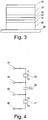
- Fig. 3 illustrates a resonator stack usable in embodiments.
- the resonator stack of Fig. 3 in embodiments may for example replace the resonator 20-22 in the cross-sectional view of Fig. 2 .
- the resonator stack of Fig. 3 comprises a first resonator formed by a first piezoelectric material 31 sandwiched between a first top electrode 30 and a first bottom electrode 32. Furthermore, the resonator stack 3 comprises a second resonator formed by a second piezoelectric material 35 sandwiched between a second top electrode 34 and a second bottom electrode 36.
- First and second resonators are separated by one or more layers 33 providing acoustic coupling and in some embodiments also electrical isolation. Layers 33 may be formed of one or more dielectric layers. Layers 33 may also comprise a combination of dielectric and conductive (e.g. metal) layers.
- the one or more layers 33 comprise at least one dielectric (electrically non-conducting) layer. Whether electrically isolating or not, the one or more layers (e.g. layer stack) 33 always provides an acoustical coupling between the first and the second resonator.
- Electrodes 30, 32, 34 and 36 each may for example comprise one or more metal layers like aluminum layers, copper layers or wolfram layers, but are not limited thereto.
- First piezoelectric material 31 and second piezoelectric material 35 in some embodiments may be the same materials. Nevertheless, in some embodiments different materials may be used.
- first piezoelectric material 31 may be a material with a comparatively low piezoelectric coupling, for example aluminum nitride, and first resonator may serve as a filter resonator as explained above to build a filter having a comparatively narrow bandwidth.
- An aluminum nitride piezoelectric layer like layer 31 may for example be produced by reactive sputtering from an Al target.
- Second piezoelectric material 35 may comprise a material having a comparatively high piezoelectric coupling, for example lithium niobate, potassium niobate or Sc-doped aluminum nitride, to provide a large tuning range.
- Sc-doped AlN layers may also be formed as so-called AlScN layers which may contain a significant amount of Sc.
- both piezoelectric layers 31, 35 may be aluminum nitride based, but with different dopants and/or dopant concentration for example different scandium (Sc) concentrations.
- the piezoelectric materials of both resonators piezoelectrically couple to a same type (polarization) of acoustic waves.
- the piezoelectric couplings generally depend on the material but also on the used crystal orientation.
- the tuning circuit of the second resonator in embodiments may only influence the frequency behavior of the first resonator if both piezoelectric layers couple to the same acoustic wave type/polarization.
- the piezoelectric layer 35 is used in a cut (crystal orientation) offering a strong piezoelectric coupling of the same polarization as piezoelectric layer 31.
- aluminum nitride may be deposited in c-axis orientation on the substrate material.
- substrate material for example substrate 25 of Fig. 2
- a silicon wafer or a lithium niobate (LiNbO 3 ) or lithium tantalate (LiTaO 3 ) crystal may be used.
- Fig. 4 illustrates an equivalent circuit of the layer stack of Fig. 3 .
- Numeral 40 denotes the first resonator, formed in Fig. 3 by layers 30, 31 and 32
- 41 denotes the second resonator, formed by layers 34, 35 and 36 in Fig. 3 .
- a terminal 43 contacts the first top electrode (30 of Fig. 3 , also labelled t 1 in Fig. 4 )
- a terminal 44 electrically contacts the first bottom electrode (32 in Fig. 3 , also labelled b 1 )
- a terminal 45 contacts the second top electrode (34 in Fig. 3 , also labelled t 2 )
- a terminal 46 electrically contacts the second bottom electrode (36 in Fig. 3 , also labelled b 2 ).
- a parasitic capacitor 42 with a capacitance C 12 is associated with the dielectric layer (stack) 33 between the first resonator's bottom electrode and the second resonators top electrode.
- first bottom electrode 32 is electrically separate from second top electrode 34
- a single electrode may be provided serving both as second top electrode and first bottom electrode, and the acoustic coupling of the resonators is then via this common electrode. In this case, no dielectric layer for electrical separation is needed.
- terminals 43 and 44 then serve to incorporate the resonator element of Fig. 4 into a filter structure.
- a tuning circuit may be coupled to terminals 45 and 46. Examples will be discussed next with reference to Figs. 5 to 7 .
- Fig. 5 illustrates an example topology of a ladder filter, in this case a 3 1 ⁇ 2 stage ladder filter.
- Numeral 50 denotes a signal input
- numeral 51 denotes a signal output
- numeral 52 denotes a ground line.
- the ladder filter of Fig. 5 comprises four series resonators 53A to 53D and three shunt resonators 54A to 54C.
- all series resonators 53A to 53D have the same resonance frequency
- all shunt resonators 54A to 54C have the same resonance frequencies, but the resonance frequencies of the series and the shunt resonators are detuned with respect to each other.
- the amount of detuning roughly corresponds to the bandwidth of the resulting filters.
- the resonance frequencies of the shunt resonators 54A to 54C in typical cases are lower than the resonance frequencies of the series resonators 53A to 53D.
- Each of resonators 53A to 53D, 54A to 54C may be a first resonator of a resonator element as discussed previously with respect to Figs. 1 , 3 and 4 . Via a tuning circuit coupled to the respective second resonator of the resonator elements, frequency tuning of the filter may be performed.
- the ladder filter structure of Fig. 5 serves only as an example, and any conventional ladder or lattice filter structures used with BAW resonators in the art may be used and modified by replacing resonators conventionally used by resonator elements comprising first and second resonators as explained with reference to Figs. 1 , 3 and 4 .
- a plurality of such filters may be combined to form an n-port filter structure, for example for filtering a plurality of frequency bands used in communication applications.
- Fig. 6 illustrates a resonator element according to an embodiment comprising a tuning circuit and usable as shunt resonator element, for example to implement shunt resonators 54A to 54C of the ladder filter structure of Fig. 5 .
- the resonator element of Fig. 6 comprises a first resonator 62 with a first top electrode t1 and a first bottom electrode b1 and a second resonator 65 with a second top electrode t2 and a second bottom electrode b2.
- First resonator 62 and second resonator 65 are electrically isolated (but not acoustically decoupled) e.g. by a dielectric material represented by a parasitic capacitance 64. This dielectric material provides an acoustic coupling between the resonators 62, 65 as indicated by an arrow 63.
- Implementation of first resonator 62 and second resonator 65 may be as explained previously with respect to Figs. 1 , 3 and 4 .
- First top electrode t1 of first resonator 62 is coupled to a first terminal 60 (also labelled “3") and a second terminal 61 (also labelled "4").
- Terminals 60, 61 serve for connection with further resonators or signal input/output terminals to build filter structures.
- first terminal 60 is coupled with series resonator 53A and second terminal 61 is coupled with series resonator 53B.
- First bottom electrode b1 of first resonator 62 is coupled to ground via a terminal 68, also labelled "0". In the example filter structure of Fig. 5 , this corresponds to the coupling of any one of shunt resonators 54A to 54C to ground line 52.
- Second top electrode t2 of second resonator 65 is coupled to ground via a terminal 69 also labelled "0".
- a tuning circuit is coupled between second top electrode t2 and second bottom electrode b2 of second resonator 65.
- the tuning circuit comprises a variable capacitor 67 coupled in parallel to an inductance 66.
- Inductance 66 in some embodiments may be implemented as a high Q (Quality-factor) inductor or other reactance, e.g. having a Q-factor of more than 10, more than 50 or more than 100.
- An inductivity L1 of the inductor may for example be between 0.5 and 200 nH, for example below 50nH, e.g. between 1 and 10 nH.
- Variable capacitor 67 may be implemented in any conventional manner using for example varactors or switched capacitors.
- tuning circuit of Fig. 6 is only an example, and various combinations of capacitances, inductors and/or resistors may be used, one or more of these capacitances, inductors and/or resistors being variable to provide a tuning.
- the tuning circuit may also comprise switches like radio frequency (RF) switches that may be selectively opened and closed to tune the resonator element.
- RF radio frequency
- capacitances or inductivities may be coupled in series or parallel to the switch or switches, (e.g. RF switch or switches).
- an inductance 66 e.g. an inductor, may increase a tuning range compared to a case where only a variable capacitor is used.
- Fig. 7 is a circuit diagram of a resonator element suitable as a series resonator in filter structures like the filter structure of Fig. 5 , for example for implementing series resonators 53A to 53D.
- the resonator element of Fig. 7 comprises a first resonator 72 and a second resonator 75 which are electrically separated as indicated by a (parasitic) capacitance 73, having a capacitance value C 12 .
- Capacitance 73 is associated with some dielectric layer(s) that acoustically couples the first resonator 72 and the second resonator 75, as indicated by an arrow 74.
- First resonator 72 has a first top electrode t1 and a first bottom electrode b1
- second resonator 75 has a second top electrode t2 and a second bottom electrode b2.
- First and second resonators 72, 75 may be implemented as explained with reference to Figs. 1 , 3 and 4 above.
- First top electrode t1 is coupled with a first terminal 70 also labelled "5", and first bottom electrode B1 is coupled with a second terminal 71, also labelled "6".
- first and second terminals 70, 71 the resonator element of Fig. 7 may be incorporated in a filter structure.
- first terminal 70 would be coupled to signal input 50
- second terminal 71 would be coupled to resonators 54A and 53B.
- resonator 54A is implemented as in Fig. 6
- second terminal 71 of Fig. 7 would be coupled with first terminal 60 of Fig. 6
- second terminal 61 of Fig. 6 would then be coupled with a corresponding terminal of resonator 53B.
- Second top electrode t2 is coupled to ground via a terminal 78, also labelled "0".
- the designations 3, 4, 5 and 6 of terminals 60, 61, 70, 71 of Figs. 6 and 7 will be used later in discussion of simulations referring to Figs. 8 to 12 , while terminals coupled to ground are also labelled "0" in Figs. 6 and 7 .
- a tuning circuit is coupled to second top electrode t2 and second bottom electrode b2 comprising for example an inductance 76 and a variable capacitor 77.
- Impedance 76 and variable capacitance 77 may be implemented in a similar manner as explained for inductance 66 and variable capacitance 67 of Fig. 6 , respectively.
- inductance 76 and capacitance 77 are merely one example for a tuning circuit coupled to second resonator 75, and as also explained for Fig. 6 other tuning circuit configurations are also possible.
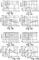
- Figs. 8(a) to 8(d) show the S-parameter (scattering parameter, representing insertion loss) over frequency for various configurations.
- the S-parameter is shown for a resonator element where the first resonator is coupled in a shunt configuration, as for example illustrated in Fig. 6 .
- Figs. 8(c) and 8(d) illustrate curves for a series coupling of a first resonator, as illustrated for example in Fig. 7.
- Figs. 8(a) and 8(b) illustrate the same curves, with the y-axis being enlarged in Fig. 8(b) compared to Fig.
- a curve 80 shows the S-parameter for a tuning circuit comprising an impedance like impedance 66 of Fig. 6 .
- the impedance in the simulation was inductivity of 1 nH with very high quality factor.
- a small capacitance 67 of 1 pF was assumed.
- a curve 81 illustrates the S-parameter with an additional capacitance of 10 pF in parallel to the impedance of curve 80. A large shift of the shown resonance of the order of 300 MHz is observed.
- a curve 82 in Figs. 8(c) and 8(d) illustrates the S-parameter for the series resonator case for a tuning circuit comprising an impedance formed by an inductivity of 1 nH with very high quality factor plus a small capacitance of 1 pF as capacitance, similar to curve 80 of Figs. 8(a) and (b) , and a curve 83 illustrates the behavior with an additional capacitance of 10 pF coupled in parallel to the impedance. Also here, a frequency shift of the resonance of the order of 300 MHz is observed.
- impedance 66 and 76, respectively, of the tuning circuit has a value of 100 nH.
- Curves 90 and 92 show the S-parameter for a capacitance of 1 pF, and curves 91 and 93 show the S-parameter for a capacitance of 10 pF. The shown resonances are shifted by less than 100 MHz both for the shunt resonator case and for the series resonator case.
- Fig. 10 shows the case for an inductivity of 3 nH.
- Curves 100 and 102 illustrate the S-parameter for a capacitance of 1 pF
- curves 101 and 103 illustrate the S-parameter for a capacitance of 10 pF.
- Each of curves 100 to 103 comprises a plurality of curves, visible in particular in the enlarged versions of graphs (b) and (d) for curves 91 and 93, respectively.
- These curves represent the behavior for different Q-factors (quality factors) of the inductivity, for a Q-factor range of 42 to 100.
- Q-factors quality factors
- the resonances in this case are shifted by about 150 MHz.
- Fig. 11 illustrates curves for an inductivity value of 1.7 nH.
- Curves 110 and 112 illustrate the S-parameter for a capacitance of 1 pF
- curves 111 and 113 illustrate the S-parameter for a capacitance of 10 pf.
- Individual curves of curves 110 to 113 visible in particular in the enlarged views of Figs. 11(b) and (d) illustrate different Q-factors for the inductivity, again in the range of 42 to 200. Through the change of capacitance, the resonance is shifted by a little less than 300 MHz.
- Fig. 12 illustrates a case with inductivity of 1.3 nH.
- Curves 120 and 122 illustrate the S-parameter for the capacitance of 1 pF
- curves 121, 123 illustrate the S-parameter for capacitance of 10 pF.
- Individual curves of curves 120 to 123 illustrate the behavior for different Q-factors.
- the resonances are shifted by almost 400 MHz.
- the difference between different Q-factors becomes more pronounced with reduced inductivities, such that in embodiments using small inductivities below 5 nH high Q-factors above 100, for example above 150, may be selected for implementing the inductivity.
- Fig. 13 illustrates the acoustic phase of a resonator stack configured as illustrated in Fig. 6 (shunt resonator configuration), with match intrinsic acoustic port terminations for the acoustic path illustrated by arrow 63.
- a curve 130 shows the phase with the tuning impedance 66, whereas a curve 131 shows the phase when capacitance 67 is additionally introduced.
- Fig. 14 illustrates a method according to an embodiment. While the method of Fig. 14 is described as a series of acts or events, the order in which these acts or events are described and shown is not to be construed as limiting. The method of Fig. 14 may be implemented using the resonator elements discussed above, and features, elements, variations and modifications described with respect to these resonator elements are also applicable to the method. For ease of reference, the method of Fig. 14 will be described referring to the previous description of resonator elements. However, the method of Fig. 14 may also be implemented independently from the resonator elements described previously.
- a resonator stack is provided.
- Providing the resonator stack may for example include forming two stacked resonators on a substrate, for example stacked resonators as discussed and described with respect to Fig. 3 .
- Providing the resonator stack may also include providing an acoustic mirror or a cavity below the resonators, as explained with reference to Fig. 2 .
- the method includes incorporating a first resonator of the resonator stack, for example the first resonator (filter resonator) of the previously discussed embodiments, in a filter structure.
- the first resonator may be included in the filter structure as a shunt resonator or as a series resonator.
- a tuning circuit is provided to a second resonator of the resonator stack, for example a tuning circuit comprising an inductor and a variable capacitor, as illustrated in Figs. 6 and 7 .
- the resonator stack may then be tuned to a desired frequency for use in the filter structure.
- the filter structure may be adapted to different frequency bands used in a communication device.
- Frequency tunable RF filters using circuit topologies with frequency tunable bulk acoustic wave (BAW) resonators have been described herein.
- Possible filter circuit topologies are, for example, ladder or lattice filters.
- the individual resonators of any filter topology differ in their respective impedance levels or, equivalently, resonator areas.
- all resonators are ideally tunable (or programmable) in a similar manner in order to enable a uniform tuning/shifting of the filter curve shown in, for example, Figs. 8(a) to Fig. 13 .
- every tunable BAW resonator has a corresponding individual tuning network, which comprises tunable or programmable capacitors and/or inductors.
- Such passive components ideally offer high quality factors in order to minimize losses and maximize the resulting (bandpass) filter performance.
- a uniform frequency tuning/shifting of the individual resonators in a filter configuration is realized by respective tuning networks that are scaled according to the associated resonator impedances.
- the capacitors in a tuning network scale proportionally to the static capacitance of the respective resonator, whereas the inductors in a tuning network scale inversely proportional to the static capacitance of the respective resonator.
- Any conventional RF filter with a topology based on fixed frequency (BAW) resonators can be converted into a tunable filter with the same topology but tunable/programmable (BAW) resonators are used instead of the fixed frequency (BAW) resonators of the conventional RF filter.
- BAW fixed frequency
- Each tunable/programmable BAW resonator is controlled by an individual tuning network.
- the impedance of each tuning network scales proportionally to the impedance of the tuning resonator (within limits according to manufacturing tolerances and parasitic effects).
- Shunt resonators may be tuned differently from the series resonators in order to allow an adjustment of the bandwidth of the frequency-shifted filter curves.
- a tunable RF ladder filter has N half stages where N ⁇ 2 is typically between 4 (e.g. 2 stages) and 7 (e.g. 3 1 ⁇ 2 stages) or 8 (e.g. 4 stages).
- a single ladder filter stage comprises a series resonator and a shunt resonator.
- a half stage may either be a series resonator or a shunt resonator.
- a 3 1 ⁇ 2 stage ladder filter may be realized with 4 shunt resonators and 3 series resonators or, alternatively, 3 shunt resonators and 4 series resonators.
- Fig. 16 shows an example of a 2 1 ⁇ 2 stage ladder filter.
- a series or shunt resonator may comprise more than one resonator in order to improve power handling capabilities, for example.
- all series resonators offer the same (series) layer stack, and all shunt resonators offer the same (shunt) layer stack.
- all series resonators offer similar resonance and anti-resonance frequencies. This is also true for all shunt resonators.
- the resonance frequencies of the shunt resonators are smaller than the respective resonance frequencies of the series resonators. (The opposite will result in bandstop filters).
- the areas of the individual resonators of a filter are different.
- the static capacitance of a resonator is proportional to its area, and the impedance function of the resonator is inversely proportional to its area.
- tunable/programmable BAW resonators of different areas offer the same frequency shifting when the impedance of their respective tuning network is proportional to the impedance of the tuning resonator.
- This kind of scaling of the tuning network's impedance with the static capacitance (or area) of the respective tuning resonator is one element for realizing frequency tunable (programmable) filters from individual frequency tunable (programmable) resonators.
- Fig. 15 illustrates an example of a tunable BAW resonator 1500 with filter resonator 1502, tuning resonator 1506, and acoustic coupling layer(s) 1504 located between filter resonator 1502 and tuning resonator 1506.
- a variable tuning circuit 1508 is coupled to the tuning resonator 1506 of the example tunable BAW resonator of Fig. 15 .
- Filter resonator 1502 includes piezoelectric layer Piezo 1 and tuning resonator 1506 includes piezoelectric layer Piezo 2.
- Also depicted in Fig. 15 is a substrate layer 1512, and an acoustic decoupling layer 1510 for acoustically decoupling the tunable BAW resonator 1500 from the substrate 1512.
- Fig. 16 shows an example of a 2 1 ⁇ 2 stage ladder filter 1600 with three series resonators 1602, 1606, and 1610, and two shunt resonators 1604 and 1608.
- Each resonator includes three elements: a filter resonator, a tuning resonator acoustically coupled to the filter resonator, and a tuning circuit electrically coupled to the tuning resonator that is described in further detail below.
- filter 1600 includes three series filter resonators 1602A, 1606A, 1610A, two shunt filter resonators 1604A, 1608A, RF input 1612 and RF output 1614.
- Each filter resonator is coupled to its own tuning network.
- Series filter resonator 1602A has a corresponding tuning network including tuning resonator 1602B coupled to tuning circuit 1602C.
- Shunt filter resonator 1604A has a corresponding tuning network including tuning resonator 1604B coupled to tuning circuit 1604C.
- Series filter resonator 1606A has a corresponding tuning network including tuning resonator 1606B coupled to tuning circuit 1606C.
- Shunt filter resonator 1608A has a corresponding tuning network including tuning resonator 1608B coupled to tuning circuit 1608C.
- Series filter resonator 1610A has a corresponding tuning network including tuning resonator 1610B coupled to tuning circuit 1610C.
- the impedance of each tuning network is scaled with the impedance (or area) of the respective resonator, in order to ensure that all individual resonators show the same (or similar) frequency tuning behavior.
- Impedance scaling ensures that there will be a uniform frequency shifting of the resulting bandpass filter curve shown in, for example, Figs. 8(a) to Fig. 13 .
- tunable resonators are chosen to simplify the filter circuit drawing of Fig. 16 .
- the "side-by-side" tunable resonator symbol is used to denote the acoustic coupling between a filter resonator and a tuning resonator.
- a tunable BAW resonator such as tunable resonator 1602
- both the filter and tuning resonators are combined and acoustically coupled in one layer stack on top of each other in an embodiment as shown in Fig. 15 .
- Frequency tunable RF filters are realized using circuit topologies with frequency tunable bulk acoustic wave (BAW) resonators with minimum parasitics, according to embodiments.
- BAW bulk acoustic wave
- Tuning networks can be realized as programmable ICs in CMOS technologies, for example.
- the ports (electrodes) of the tuning resonators should ideally be realized with minimum parasitics, i.e. with minimum resistive losses. Therefore, the ports (electrodes) of the tuning resonators should be close to the surface of the BAW chip.
- the filter resonators should be located (fabricated) close to the substrate (with acoustic mirror or membrane/cavity for acoustic decoupling) and directly connected within their (buried) electrode metallization layers. The tuning resonators are then located (fabricated) on top of their respective filter resonators at/near the surface of the substrate.
- the interconnects between the tuning resonators and their tuning networks are as short and low-ohmic as possible, because deep vias are not required as in the case of tunable BAW resonators with filter resonators on top of their respective tuning resonators.
- Embodiments discussed below especially suit to filter implementations where every tunable BAW resonator requires its own tuning network.
- a ladder filter with N resonators needs 2*N interconnects to the tuning circuits, but only one interconnect (via) for the filter input, and one interconnect (via) for the filter output (plus ground connection).
- each tunable BAW resonator is characterized by a layer stack in which the tuning resonator is positioned on top of the filter resonator; the individual tunable BAW filter resonators are coupled to each other within their respective electrode layers (some vias between these two electrode layers might be required in order to realize a specific filter topology, but such vias have a length determined by the piezoelectric layer thickness of the filter resonator and are thus quite short/shallow, typically around 1 ⁇ m); only the filter input and the filter output terminals are coupled by deep vias to the surface of the BAW filter chip, which minimizes the numbers of deep vias needed to combine the filter resonators to the filter circuit; and the tuning resonators of the individual tunable BAW resonators are all realized on top
- the interconnects of the tuning resonators to their respective tuning networks are as short as possible (at or near the chip surface) with only shallow vias for contacting the tuning resonator bottom electrodes.
- Such a configuration is extremely helpful for the tunable resonator performance and thus the overall filter performance.
- Fig. 17 shows an example of tunable BAW resonator 1700 with the tuning resonator 1702 on top of the filter resonator 1706 according to an embodiment. Also shown in Fig. 17 are the acoustic coupling layer 1704 and the tuning circuit 1708.
- the stacked layer construction shown in Fig. 17 is superior to the standard stacked layer construction 1500 of Fig. 15 in some respects as interconnects between the tuning networks and the tuning resonators are much easier to realize, and offer the additional advantage of smaller parasitics (especially ohmic losses).
- each tuning resonator can be easily coupled with each other according to the filter topology to be realized by utilizing their electrode metallization layers (optionally in combination with some shallow vias between such electrode layers in some embodiments), thereby minimizing the overall number of vias, as will be explained in further detail below with respect to Fig. 18A .
- each tuning resonator is coupled to its own tuning network.
- Fig. 18A illustrates a schematic cross-sectional view through an integrated circuit filter 1800 having tunable resonators 1812, 1814, and 1816.
- each tunable resonator includes a filter resonator, a tuning resonator, and a tuning circuit coupled in the manner previously discussed.
- Tunable resonator 1812 therefor includes a filter resonator 1812A, a tuning resonator 1812B, and a tuning circuit 1812C.
- Tunable resonator 1814 includes a filter resonator 1814A, a tuning resonator 1814B, and a tuning circuit 1814C.
- Tunable resonator 1816 includes a filter resonator 1816A, a tuning resonator 1816B, and a tuning circuit 1816C.
- Filter resonator 1812A is a shunt resonator coupled between ground (through bottom electrode 1832 and deep via 1828A) and RF IN (through top electrode 1834 and shallow via 1824).
- the top electrode 1834 of filter resonator 1812A is coupled to the top electrode 1834 of filter resonator 1814A as shown.
- Filter resonator 1814A is a series resonator coupled between filter resonator 1812A (in shunt configuration with top electrode 1834 coupled to RF In port 1808) and filter resonator 1816A (in shunt configuration with bottom electrode 1824 coupled to ground through deep via 1828B and top electrode 1822 coupled to the RF Out port 1810 through shallow via 1826).
- the top electrode 1822 of the shunt filter resonator 1816A is coupled to the bottom electrode 1820 of the series resonator 1814A. This connection uses a via 1830 between the respective electrode contacts 1820 and 1822.
- the electrical coupling between electrodes of individual filter resonators can be realized by appropriate structuring of the respective metallization layers used for such electrodes. Realization of a filter circuit by coupling of series and shunt filter resonators can thus be achieved using a number of shallow vias and only two deep vias as shown.
- acoustic decoupling layers 1836A, 1836B and 1836C are acoustic decoupling layers 1836A, 1836B and 1836C.
- Decoupling layer 1836A is used for decoupling resonator 1812 from substrate 1802.
- Decoupling layer 1836B is used for decoupling resonator 1814 from substrate 1802.
- Decoupling layer 1836C is used for decoupling resonator 1816 from substrate 1802.
- the tuning resonators 1812B, 1814B, and 1816B are placed on top of the corresponding resonator stacks 1812A, 1814A, and 1816A, which results in short and low-ohmic interconnects to the tuning networks 1812C, 1814C, and 1816C.
- the filter resonators 1812A, 1814A, 1816 are located in the deeper regions of the resonator's layer stacks, closer to the substrate 1802 and the acoustic decoupling provided by a cavity or an acoustic mirror (shown in Fig. 18A as acoustic decoupling layers 1836A, 1836B, and 1836C previously described, in an embodiment).
- the filter resonators are interconnected with each other according to the filter circuit topology.
- Filter resonators 1812A and 1814A are coupled together with interconnect 1834
- filter resonators 1814A and 1816A are coupled together with interconnects 1820, 1822, and shallow via 1830.
- Such interconnects can be performed within the electrode metallization layers of the filter resonator without any via or with only a small number of (shallow) vias between the two electrode metallizations (depending on the filter topology).
- Deeper vias 1828A and 1828B are only needed for contacting RF In and RF Out in some embodiments, and for the ground connection for the embodiment shown in Fig. 18A .
- filter resonators 1812A, 1814A, 1816A are shown as being formed (or embedded) in an insulating layer 1804.
- the insulating layer can comprise, for example silicon dioxide or other known insulating materials.
- Acoustic coupling layer is shown as a common acoustic coupling layer 1806 for acoustically coupling the filter resonators and the tuning resonators.
- Tuning circuits 1812C, 1814C, and 1816C can at least partially be implemented using the same fabrication process as for the integrated circuit filter 1800. Alternatively, different fabrication processes can be used to realize the tuning circuits as is discussed in further detail below.
- Fig. 18B reproduces the filter circuit of Fig. 18A , with the filter resonators 1812A, 1814A, and 1816A being highlighted with corresponding circle symbols (1), (2), and (3).
- the corresponding electrical schematics are also shown, with the left-hand schematic preserving the physical orientation of filter resonators 1812A, 1814A, and 1816A, and the right-hand schematic shown in a more conventional manner.
- the shunt resonators 1812A and 1816A and the series resonator 1814A are clearly shown coupled between RF IN port 1808 and RF OUT port 1810 in a ladder filter configuration.
- tunable BAW resonators can be realized as a pair of coupled BAW resonators.
- One resonator is the filter resonator, i.e. the resonator to build into filter circuit topologies.
- the other acoustically coupled BAW resonator is the tuning resonator.
- the tuning resonator is coupled to a tuning network.
- the tuning resonator combined with the tuning network effectively act as tuning layer within the filter resonator layer stack.
- This tuning layer offers a tunable mechanical stiffness.
- the tunable mechanical stiffness depends on the tuning network settings and affects the acoustic velocities and the acoustic impedance of the tuning layer.
- a composite BAW resonator 1900 includes two (instead of only one, see for example Figs. 15 and 17 ) tuning resonators 1902 and 1912 inside the layer stack of the tunable resonator 1900.
- the two tuning resonators 1902 and 1912 are placed on both sides on the filter resonator, i.e. one tuning resonator (top tuning resonator 1902) above the filter resonator 1908 and the second tuning resonator (bottom tuning resonator 1912) below the filter resonator.
- tuning layers with tunable mechanical stiffness are placed on both sides (top and bottom) of the filter resonator.
- top tuning resonator includes a piezoelectric layer Piezo 1 and is coupled to a tuning circuit 1904.
- Filter resonator 1908 includes a piezoelectric layer Piezo 2.
- Bottom tuning resonator includes a piezoelectric layer Piezo 3 and is coupled to a tuning circuit 1914.
- Acoustic coupling layer 1906 acoustically couples top tuning resonator 1902 and filter resonator 1908.
- Acoustic coupling layer 1910 acoustically couples bottom tuning resonator 1912 to filter resonator 1908.
- acoustic coupling layer 1906 is coupled between a bottom electrode of top tuning resonator 1902 and a top electrode of filter resonator 1908.
- acoustic coupling layer 1910 is coupled between a bottom electrode of filter resonator 1908 and a top electrode of bottom tuning resonator 1912.
- the areas of resonators 1902, 1908, and 1912 are matched.
- the static capacitances of the filter resonator 1908 and the two tuning resonators 1902 and 1912 depend on the area, but also on the thicknesses and the dielectric constants of the individual piezoelectric layers resp. materials, and typically differ from each other.
- the filter signal terminals are associated with the top and bottom electrodes of the filter resonator.
- Resonator 1900 can be used as desired in a ladder filter as previously described.
- Fig. 19 Also shown in Fig. 19 is the substrate layer 1918, and the acoustic decoupling layer 1916 for acoustically decoupling resonator 1900 from the substrate 1918.
- the composite resonator 1900 of Fig. 19 is a layer stack in an embodiment that provides an enhanced tuning range compared with the single tuning resonator embodiments shown in Figs. 15 and 17 .
- a tuning circuit with enhanced tuning range including an inductor provides a tuning range improvement over a tuning circuit including only a variable capacitor.
- An inductor with a high Q (quality factor) can be integrated on a piezoelectric die with the corresponding resonator, an interposer material, an RF filter control chip or an IPD (integrated passive device), according to whichever available manufacturing process provides the best metal layers for the inductor.
- Metal layers with low resistivity can be used in order to design high Q inductors. For example, thick copper or aluminum metal layers can be patterned into high Q inductors suitable for use in the tuning circuit.
- An inductor Q of 30 to 50 may enable an increase of the total tuning range by a factor of 1.5, for example.
- the tuning network is complemented with a high Q inductor which is integrated on the Piezoelectric die ( Fig. 23 ) or the interposer material ( Fig. 24 ) or the RF Filter control chip ( Fig. 25 or 26 ) or an IPD ( Fig 25 or 26 ) as will be explained in further detail below.
- Fig. 20A illustrates a tunable BAW resonator 2000A with a filter resonator 2002, a tuning resonator 2004, and acoustic coupling layer(s) 2006 therebetween.
- Filter resonator 2002 includes a top electrode t1, a piezoelectric layer Piezo 1, a bottom electrode b1, and is located above acoustic coupling layer 2006 in a layer stack.
- Tuning resonator 2004 includes a top electrode t2, a piezoelectric layer Piezo 2, a bottom electrode b2, and is located below acoustic coupling layer 2006 in the layer stack.
- a tuning network (with tunable/programmable impedance) Zt is coupled to tuning resonator 2004.
- tuning network Zt includes both an inductor and a variable capacitor.
- Fig. 20B illustrates a tunable BAW resonator 2000B with a filter resonator 2002, a tuning resonator 2004, and acoustic coupling layer(s) 2006 therebetween.
- Filter resonator 2002 includes a top electrode t2, a piezoelectric layer Piezo 2, a bottom electrode b2, and is located below acoustic coupling layer 2006 in the layer stack.
- Tuning resonator 2004 includes a top electrode t1, a piezoelectric layer Piezo 1, a bottom electrode b1, and is located above acoustic coupling layer 2006 in the layer stack.
- a tuning network Zt is coupled to tuning resonator 2004.
- tuning network Zt includes both an inductor and a variable capacitor.
- Figs. 21A through 21D illustrate that acoustically coupled resonator devices can be in a shunt or a series configuration.
- Figs. 21A and 21B show the shunt configuration (with one electrode of the filter resonator grounded), whereas Figs. 21C and 21D show the series configuration.
- the electric ports have the reference numbers 1 and 2.
- Zt is an impedance, which is coupled in parallel to the two electrodes of the tuning resonator.
- Zt could include a high-Q inductor Lt, and a variable capacitor Ct could be implemented by a programmable capacitor, like a C-tuner available from Infineon Technologies.
- the acoustic coupling layer is shown having a static capacitance of C12 and an acoustic coupling component ka12.
- Each tuning resonator is shown as being coupled to corresponding tuning circuit Zt.
- Fig. 21A shows a shunt resonator 2100A with the filter resonator 2002 in the top position and the tuning resonator 2004 in the bottom position in a layer stack.
- Fig 21B shows a series resonator 2100B with the filter resonator 2002 in the top position and the tuning resonator 2004 in the bottom position in the layer stack.
- Fig 21C shows a shunt resonator 2100C with the filter resonator 2002 in the bottom position and the tuning resonator 2004 in the top position in the layer stack.
- Fig 21D shows a series resonator 2100D with the filter resonator 2002 in the bottom position and the tuning resonator 2004 in the top position in the layer stack.
- Fig. 22 illustrates an example of a 1 1 ⁇ 2 stage ladder filter 2200 with one series tunable resonator 2208 (filter resonator 2208A, tuning resonator 2208B, variable capacitor 2208C, and inductor 2208D) and two shunt tunable resonators 2206 (filter resonator 2206A, tuning resonator 2206B, variable capacitor 2206C, and inductor 2206D) and 2210 (filter resonator 2210A, tuning resonator 2210B, variable capacitor 2210C, and inductor 2210D).
- Each tunable resonator includes a filter resonator and a tuning resonator that is coupled to a tuning circuit that comprises a variable capacitor and an inductor.
- Also shown in Fig. 22 are an RF In port 2202 and an RF Out port 2204.
- each tuning network scales inversely with the static capacitance (or area) of the respective tuning resonator, in order to ensure that all individual resonators show the same (or similar) frequency tuning behavior.
- Matching tuning impedances ensures a uniform frequency shifting of the resulting bandpass filter curve.
- the tuning range of the equivalent filter can be increased significantly. It is important to note that the symbols used for the tunable resonators are chosen to simplify the filter circuit drawing. For the tunable BAW resonator, both of the filter and tuning resonators are combined and acoustically coupled in a layer stack on top of each other as has been described herein.
- Fig. 23 illustrates in an integrated circuit example of a 1 1 ⁇ 2 stage ladder filter 2300 with one tunable series resonator 2312 (filter resonator 2312A, tuning resonator 2312B, variable capacitor 2312C, and inductor 2312D) and two shunt tunable resonators 2310 (filter resonator 2310A, tuning resonator 2310B, variable capacitor 2310C, and inductor 2310D) and 2314 (filter resonator 2314A, tuning resonator 2314B, variable capacitor 2314C, and inductor 2314D).
- tuning impedance Zt, Lt is integrated on the piezoacoustic die, preferable with a thick layer of metal with very low resistance in order to achieve very high Q inductors (Ql > 15, wherein Ql is the loaded quality factor).
- Ql is the loaded quality factor.
- the capacitive portion of tuning impedance Zt, Ct is illustrated as a varactor in Fig. 23 .
- Fig. 23 illustrates a cross-sectional view of a piezoacoustic die including a substrate 2302, an insulating layer 2304 including filter resonators 2310A, 2312A, 2314A, acoustic coupling layer 2306, and insulating layer 2308 including tuning resonators 2310B, 2312B, 2314B.
- Metalized via 2316 is configured for providing an RF input and contacts an upper electrode of filter resonators 2310A and 2312A.
- Metalized via 2318 is configured for providing an RF output and contacts a bottom electrode of filter resonators 2312A and 2314A.
- Metalized vias 2310E and 2310F are configured to electrically contact tuning resonator 2310B and variable capacitor 2310C and inductor 2310D.
- Metalized vias 2312E and 2312F are configured to electrically contact tuning resonator 2312B and variable capacitor 2312C and inductor 2312D.
- Metalized vias 2314E and 2314F are configured to electrically contact tuning resonator 2314B and variable capacitor 2314C and inductor 2314D.
- Fig. 23 shows an implementation of variable capacitors 2310C, 2312C, 2314C and inductors 2310D, 2312D, 2314D on an upper surface 2320 of integrated circuit filter 2300.
- inductors 2310D, 2312D, and 2314D are shown as patterned metal traces using a metal layer that would be available in the piezoacoustic integrated circuit process used to fabricate the lower layers of the chip.
- Inductors 2310D, 2312D, 2314D include a corresponding crossover 2310G, 2312G, 2314G so that the innermost coil of the inductor can be electrically contacted.
- variable capacitors 2310C, 2312C, and 2314C are fabricated on a different chip and electrically coupled to 2310E/2310F, 2312E/F, and 2314E/F, respectively.
- Variable capacitors 2310C, 2312C, and 2314C can be fabricated as varactors using a capacitor-connected transistor, in an embodiment.
- Fig. 24 illustrates an example of a 1 1 ⁇ 2 stage ladder filter 2400 fabricated in a piezoacoustic chip including layers 2302, 2304, 2306, and 2308 as previously described with respect to Fig. 23 , but where the inductive part of Zt, Lt is integrated on an interposer metal layer (on e.g. laminate) 2324.
- the inductor metal layer may not be available on the piezoacoustic chip, but is available on the interposer 2324.
- a thick layer of metal with very low resistance is preferred in order to achieve very high Q inductors (Ql > 15).
- Ql > 15 The capacitive portion of Zt, Ct is just illustrated as a varactor in the block diagram.
- a metalized through-via 2330 is used to provide an RF In port in an embodiment.
- a metalized through-via 2328 is used to provide an RF Out port in an embodiment.
- Interposer 2324 includes an additional plurality of metalized through-vias for contacting varactors 2310C, 2312C, 2314C and inductors 2310D, 2312D, 2314D shown in a plan view below.
- Interposer 2324 includes a top surface 2326 for fabricating the inductors and connecting the variable capacitors. Also shown in the top portion of Fig. 24 is a ball grid array 2322 for electrically contacting the corresponding through-vias in the interposer 2324.
- FIG. 24 shows the top surface 2326 of the interposer 2324 including the mounted/attached/coupled variable capacitors 2310C, 2312C, 2314C, and the corresponding coupled inductors 2310D, 2312D, and 2314D, fabricated as part of the interposer 2324 or 2326, respectively.
- the inductors include corresponding crossovers 2310G, 2312G, 2314G whose function was previously described with respect to Fig. 23 .
- Fig. 25 illustrates an example of a 1 1 ⁇ 2 stage ladder filter 2500 with one series tunable resonators and two shunt tunable resonators.
- the inductive part of Zt, Lt is integrated on thick metal layer(s) of a filter control chip with very low resistance or a high Q IPD with very low resistance through an interposer material (e.g. two layer laminate) in order to achieve very high Q inductors (Ql > 15).
- the capacitive portion of Zt, Ct is illustrated as a varactor in Fig. 25 .
- FIG. 25 shows a cross-sectional view of the construction of the ladder filter 2500 according to an embodiment.
- the piezoacoustic chip including interconnected layers 2302, 2304, 2306, and 2308 all previously discussed, as well as ball grid array 2322.
- An interposer 2324 includes a plurality of through-vias for coupling the piezoacoustic chip to the IPD 2334.
- IPD 2334 includes variable capacitors 2310C, 2312C, 2314C and inductors 2310D, 2312D, 2314D, as well as ball grid array 2332.
- the inductors and variable capacitors in IPD 2334 can be fabricated within or on top the IPD according to the IPD process used.
- Fig. 25 shows a plan view of the IPD 2334 including variable capacitors 2310C, 2312C, and 2314C, and inductors 2310D, 2312D, and 2314D.
- Fig. 26 illustrates an example of a 1 1 ⁇ 2 stage ladder filter 2600 substantially as described with respect to Fig. 25 .
- the IPD 2334 is coupled directly to ball grid array 2332 as shown, and interposer 2324 is removed.
- the upper portion of Fig. 26 is a cross-sectional view of the ladder filter 2600, and the bottom portion of Fig. 26 is a plan view of the IPD 2334 as previously described.
- a tuning circuit is provided only to the second or third resonators of the respective resonator elements, in other embodiments of resonator elements and methods in addition a further tuning circuit may be provided to the first resonator element.
- the further tuning circuit may be implemented in a similar manner as has been explained above for the tuning circuit, e.g. as an impedance network.
- filters using resonator elements as described above may in particular be used in communication devices like mobile communication devices, and such communication devices using corresponding filter structures may form embodiments, the filters may also be used in other devices where signals, in particular high frequency signals in GHz-range, are to be filtered.
Abstract
Description
- The present application relates to tunable resonator elements, filters using such tunable resonator elements and corresponding methods.
- Filters are used in a variety of electronic circuits to filter out certain frequency components of a signal while letting other frequency components pass. For example, in communication circuits filters may be used to block frequency components outside a frequency band or part of a frequency band used for communication and to be processed by further circuits.
- To increase bandwidth, communication standards like wireless communication standards (e.g. LTE, Long-Term Evolution) or also wire-based communication standards continually increased a used frequency range and a number of used frequency bands. In communication devices implementing such standards, often highly selective filters matched to the respective frequency bands are required. The frequency bands used may differ from country to country. Therefore, a plurality of filters having different filter characteristics (for example different passbands) is required. Furthermore, in what is referred to as carrier aggregation several frequency bands are operated at the same time. This requires specific filter designs for exactly those combinations. With a specific filter provided for each possible combination, the number of physical filters is actually much higher than the number of available bands. In order to reduce the number of different filters (two-port up to n-port filters) actually required in a communication device, tunable filters are highly desirable.
- As highly selective band pass filters in communication circuits and devices, surface acoustic wave (SAW) or bulk acoustic wave (BAW) technologies are frequently used. Conventional filters of such types are designed for fixed resonance or center frequencies. As a consequence, many filters are required to serve individual frequency bands or aggregated combinations of several frequency bands used in current communication standards like LTE, including WiFi. Radio frequency (RF) switches are then used to select individual filters of the plurality of filters for example for a desired signal path between an antenna and a low noise amplifier or power amplifier. Therefore, in such conventional approaches a large number of mostly discrete components is required, increasing circuit complexity, radio frequency losses, manufacturing complexity and the needed space for radio frequency front ends in communication devices. Space is limited in mobile devices such as smartphones, and therefore tunable solutions are highly desired to save area.
- Some approaches have been made to make such SAW or BAW filters tunable in order to decrease the overall number of filters required. However, conventional tuning techniques may have drawbacks regarding their tuning range, their selectivity and/or regarding losses introduced by the possibility of tuning the filter. Therefore, it is an object to provide improved possibilities for filter tuning.
- An RF integrated circuit filter as defined in
claim 1, an RF filter device as defined inclaim 8 and an RF filter as defined inclaim 14 are provided. The dependent claims define further embodiments. - In accordance with an embodiment, a resonator element for a filter includes a first resonator having a first terminal and a second terminal for coupling to a filter structure; a second resonator having a third terminal and a fourth terminal, where the second resonator is acoustically coupled to the first resonator; and a tuning circuit coupled to the third and fourth terminals. In one embodiment, a third resonator is coupled to the first resonator. In one embodiment, the tuning circuit includes at least one of a variable capacitor and an inductor.
- In accordance with another embodiment, an RF filter device, includes a signal input; a signal output; a plurality of series resonator elements coupled between the signal input and the signal output, wherein each series resonator element comprises a first resonator having a first terminal and a second terminal, a second resonator having a third terminal and a fourth terminal, wherein the second resonator is acoustically coupled to the first resonator, and a tuning circuit coupled to the third and fourth terminals; and a plurality of shunt resonator elements coupled to the plurality of series resonator elements, wherein each shunt resonator element comprises a first resonator having a first terminal and a second terminal, a second resonator having a third terminal and a fourth terminal, wherein the second resonator is acoustically coupled to the first resonator, and a tuning circuit coupled to the third and fourth terminals.
- In accordance with another embodiment, an RF integrated circuit filter includes a substrate; an insulating layer arranged on the substrate; a plurality of filter resonators arranged in the insulating layer including a patterned top electrode layer, a patterned piezoelectric layer, and a patterned bottom electrode layer, wherein at least two of the plurality of filter resonators are coupled together with the patterned top electrode layer; an acoustic coupling layer arranged on the plurality of filter resonators; and a plurality of tuning resonators arranged on the acoustic coupling layer and correspondingly located above each of the plurality of filter resonators.
- In accordance with another embodiment, an RF filter device includes a signal input; a signal output; and a resonator element coupled between the signal input and the signal output, wherein the resonator element comprises a first resonator, a second resonator above the first resonator, wherein the second resonator is acoustically coupled to the first resonator, a third resonator below the first resonator, wherein the third resonator is acoustically coupled to the first resonator, a first tuning circuit coupled to second resonator; and a second tuning circuit coupled to the third resonator.
- In accordance with another embodiment, an RF filter includes a substrate; an insulating layer on the substrate; a plurality of filter resonators in the insulating layer including a patterned top electrode layer, a patterned piezoelectric layer, and a patterned bottom electrode layer, wherein at least two of the plurality of filter resonators are coupled together with the patterned top electrode layer and at least two of the plurality of filter resonators are coupled together with the patterned bottom electrode layer; an acoustic coupling layer on the plurality of filter resonators; a plurality of tuning resonators on the acoustic coupling layer correspondingly located above each of the plurality of filter resonators; and a plurality of tuning circuits coupled to the plurality of tuning resonators, wherein each tuning circuit comprises a variable capacitor and an inductor.
- For a more complete understanding of the present invention, and the advantages thereof, reference is now made to the following descriptions taken in conjunction with the accompanying drawings, in which:
-
Fig. 1 is a schematic block diagram of a resonator element according to an embodiment; -
Fig. 2 is a schematic cross-sectional view illustrating implementation of a resonator; -
Fig. 3 is a schematic cross-sectional view of a resonator stack usable in embodiments; -
Fig. 4 is an example equivalent circuit of the resonator stack ofFig. 3 ; -
Fig. 5 is an example filter structure which may be implemented using resonator elements according to embodiments; -
Fig. 6 is a circuit diagram of a resonator element according to an embodiment usable as shunt resonator element; -
Fig. 7 is a circuit diagram of a resonator element according to an embodiment usable as series resonator element; -
Figs. 8 to 13 illustrate simulation results to illustrate operation of embodiments; -
Fig. 14 is a flow chart illustrating a method according to an embodiment; -
Fig. 15 is a cross-sectional diagram of a resonator element including a filter resonator in a top position in a layer stack and a tuning resonator in a bottom position in the layer stack, and a tuning circuit coupled to the tuning resonator; -
Fig. 16 is a schematic diagram of a 2 ½ stage ladder filter, wherein each resonator element includes a filter resonator and a corresponding tuning resonator coupled to a tuning circuit; -
Fig. 17 is a cross-sectional diagram of a resonator element including a filter resonator in a bottom position in a layer stack and a tuning resonator in a top position in the layer stack, and a tuning circuit coupled to the tuning resonator; -
Fig. 18A is a cross-sectional diagram of a 1 ½ stage ladder filter integrated circuit, wherein each resonator element includes a filter resonator and a corresponding tuning resonator coupled to a tuning circuit, and deep vias that are used to provide ground access; -
Fig. 18B is a schematic diagram corresponding to the ladder filter ofFig. 18A ; -
Fig. 19 is a cross-sectional diagram of a resonator element in a layer stack including a first tuning resonator in a top position coupled to a first tuning circuit, a filter resonator in a middle position, and a second tuning resonator in a bottom position coupled to a second tuning circuit; -
Fig. 20A and Fig. 20B show cross sectional diagrams of resonator element layer stacks including tuning resonators in top and bottom positions, coupled to a corresponding tuning network Zt; -
Figs. 21A through 21D are circuit diagrams of shunt and series resonator elements including tuning resonators in either a top position or in a bottom position, coupled to a corresponding tuning network Zt including a variable capacitor and an inductor; -
Fig. 22 is a schematic diagram of a 1 ½ stage ladder filter, wherein each filter resonator includes a corresponding tuning resonator coupled to a tuning circuit, the tuning circuit including a variable capacitor and an inductor; and -
Figs. 23 through 26 illustrate various integrated circuit implementations of the ladder filter ofFig. 22 . - In the following, various embodiments will be described in detail referring to the attached drawings. It should be noted that these embodiments serve illustrative purposes only and are not be construed as limiting. For example, while embodiments may be described as comprising a plurality of features, elements or details, in other embodiments some of these features, elements or details may be omitted and/or may be replaced by alternative features, elements or details. In addition to the features, elements or details explicitly described, other features, elements or details, for example components conventionally used in bulk acoustic waves (BAW)-based filters, may be provided.
- Features from different embodiments may be combined to form further embodiments unless noted to the contrary. Variations or modifications described with respect to one of the embodiments may also be applicable to other embodiments unless noted otherwise.
- Embodiments discussed in the following relate to bulk acoustic wave (BAW) resonator elements which may be used to build a BAW-based filter. For forming BAW resonators, generally a piezoelectric layer is provided between two electrodes. The application of an electric field between the two electrodes generates a mechanical stress that is further propagated through the bulk of the structure as an acoustic wave. A resonance condition is established when the acoustical path and thickness direction of the structure corresponds to integer multiples of half the acoustic wave length.
- In embodiments, at least two resonators are used which are acoustically coupled to each other to form a resonator element. A first resonator of the two resonators has terminals to be incorporated in a filter structure. A second resonator is coupled to a tuning circuit. Via the tuning circuit, the position of resonances of the resonator element may be modified.
- In addition, in some embodiments the first resonator may be coupled to a further tuning circuit
Fig. 1 schematically illustrates such a resonator element according to an embodiment. The resonator element of the embodiment ofFig. 1 comprises afirst resonator 10 which is coupled with asecond resonator 14 via anacoustic coupling 13. Acoustic coupling means in this context that acoustic waves offirst resonator 10 may at least partially propagate tosecond resonator 14 and vice versa. Such an acoustic coupling between resonators may for example be implemented using a dielectric material. -
First resonator 10 has afirst terminal 11 and asecond terminal 12. Using first andsecond terminals first resonator 10, the resonator element ofFig. 1 may be incorporated in a filter structure like a ladder filter structure or a lattice filter structure. - Furthermore, a
tuning circuit 15 is coupled tosecond resonator 14.Tuning circuit 15 may comprise an impedance network, which may comprise variable elements like variable impedances, for example a variable capacitor, or switches like radio frequency (RF) switches. By changing a value of the variable element(s) of tuningcircuit 15, resonances of the resonator element ofFig. 1 may be shifted. This may be used for building a tunable filter using one or more resonator elements as shown inFig. 1 . - It should be noted that in contrast to some conventional approaches, tuning
circuit 15 is electrically decoupled fromfirst resonator 10 and acts on thefirst resonator 10 only viasecond resonator 14 andacoustic coupling 13. In some embodiments, this avoids adverse effects compared to tuning circuits directly coupled tofirst resonator 10. - In some embodiments,
first resonator 10 andsecond resonator 14 may be similar resonator structures using similar materials. In other embodiments, different materials may be used. For example, in an embodiment for first resonator 10 a material with a comparatively low piezoelectric coupling may be used, for example aluminum nitride (AlN). This allows for building filters having a small bandwidth. On the other hand, in embodiments,second resonator 14 may be build based on a material having a comparatively high piezoelectric coupling, for example lithium niobate (LiNbO3) or potassium niobate (KNbO3) or Sc-doped aluminum nitride or aluminum scandium nitride AlScN. This in some embodiments allows for a high tuning range. In some embodiments, the piezoelectric coupling constant kT 2 for the piezoelectric material of the first resonator may be below 30%, for example below 20% or below 10%, while the piezoelectric coupling constant kT 2 the second resonator may be above 10%, for example above 20%, for example above 30% or above 40%. The piezoelectric (electromechanical) coupling constant kT 2 may be calculated from the tensor properties of the respective piezoelectric material, i.e. from elastic stiffness or compliance coefficients, dielectric coefficients, and piezoelectric coefficients. Constant kT 2 is also referred to as a piezoelectric coupling constant for a transversely clamped material; kT 2 may be defined as kT 2=K2/(1+K2), where piezoelectric coupling constant K2 is defined as K2=e2/(□S cE), e is the piezoelectric material coefficient, □S the dielectric material coefficient and cE is the elastic material coefficient of the respective piezoelectric material used. - The piezoelectric coupling constant kT 2 is a measure for the relative bandwidth of an (ideal) piezoelectric resonator. Therefore, in embodiments combinations of different materials for
first resonator 10 andsecond resonator 14 allow on the one hand a small bandwidth, as required for some communication applications, and on the other hand allows for a comparatively wide tuning range. Using an aluminum nitride based resonator asfirst resonator 10 in embodiments additionally provides a good thermal conduction capable of transporting heat, which may be important for some applications to be able to prevent overheating. However, the above materials are to be taken merely as examples, and other materials may also be used. -
First resonator 10 may also be referred to as filter resonator, as it is to be incorporated into a filter structure using first andsecond terminals Second resonator 14 may also be referred to as a frequency tuning resonator, as it is used for tuning resonance frequencies of the resonator element ofFig. 1 usingtuning circuit 15. -
First resonator 10,acoustic coupling 13 andsecond resonator 14 may be implemented in a single material stack using existing process flows. - Corresponding stack structures will be discussed next with reference to
Figs. 2 and3 . As an introduction,Fig. 2 shows a resonator element with a single resonator for explanatory purposes. Then, referring toFig. 3 a resonator stack comprising first and second resonators (forexample resonators Fig. 1 ) will be explained. -
Fig. 2 illustrates a cross-sectional view of a bulk acoustic wave (BAW) resonator. The resonator itself comprises apiezoelectric material 21 sandwiched between atop electrode 20 and abottom electrode 22.Top electrode 20 andbottom electrode 22 may each be formed by one or more metal layers. - Instead of single resonator as illustrated in
Fig. 2 , in some embodiments a resonator stack comprising a first resonator and a second resonator is provided, as will be explained in below inFig. 3 . - In the embodiment of
Fig. 2 , for acoustic isolation of the resonator a so-called acoustic mirror is placed below the resonator. The acoustic mirror ofFig. 2 comprises a sequence of layers with alternating low and high acoustic impedances. For example, inFig. 2 numeral 23 designates a material with a comparatively low acoustic impedance, whereas 24A to 24C designate layers with a comparatively high acoustic impedance, leading to alternating layers of low and high acoustic impedance below theresonator material 23 betweenlayers electrode 22 and asubstrate 25 as well aslayers 24A to 24C themselves) in embodiments has a thickness of approximately λ/4, λ being the acoustic wavelength of a longitudinal wave within the layer. In this respect, it should be noted that λ depends on the respective layer material. This acoustic mirror structure acoustically decouples the resonator from the supportingsubstrate 25. Instead of such an acoustic mirror, in other embodiments also a cavity may be provided. The cavity may be directly underneath thebottom electrode 22, or under a thin membrane which supports theresonator structure 20/21/22. - The resonance frequencies of a resonator as illustrated in
Fig. 2 comprisingtop electrode 20,piezoelectric material 21 andbottom electrode 22 depends on the thicknesses of all these discussed layers, where the piezoelectric layer thickness has the largest influence, followed by electrode thicknesses. Therefore, in case ofFig. 2 in the absence of further circuits influencing the frequency the resonance frequencies of the resonator are fixed for a specific combination of materials and layer thicknesses and may be changed only by physically changing the structure, for example using processing steps like deposition or etching (as global measures or as local measures defined by lithography). -
Fig. 3 illustrates a resonator stack usable in embodiments. The resonator stack ofFig. 3 in embodiments may for example replace the resonator 20-22 in the cross-sectional view ofFig. 2 . - The resonator stack of
Fig. 3 comprises a first resonator formed by a firstpiezoelectric material 31 sandwiched between a firsttop electrode 30 and a firstbottom electrode 32. Furthermore, theresonator stack 3 comprises a second resonator formed by a secondpiezoelectric material 35 sandwiched between a secondtop electrode 34 and a secondbottom electrode 36. First and second resonators are separated by one ormore layers 33 providing acoustic coupling and in some embodiments also electrical isolation.Layers 33 may be formed of one or more dielectric layers.Layers 33 may also comprise a combination of dielectric and conductive (e.g. metal) layers. In embodiments where electric isolation betweenbottom electrode 32 andtop electrode 34 is required (as it is the case for series resonator elements), the one ormore layers 33 comprise at least one dielectric (electrically non-conducting) layer. Whether electrically isolating or not, the one or more layers (e.g. layer stack) 33 always provides an acoustical coupling between the first and the second resonator. -
Electrodes piezoelectric material 31 and secondpiezoelectric material 35 in some embodiments may be the same materials. Nevertheless, in some embodiments different materials may be used. For example, as already explained with reference toFig. 1 , firstpiezoelectric material 31 may be a material with a comparatively low piezoelectric coupling, for example aluminum nitride, and first resonator may serve as a filter resonator as explained above to build a filter having a comparatively narrow bandwidth. An aluminum nitride piezoelectric layer likelayer 31 may for example be produced by reactive sputtering from an Al target. Secondpiezoelectric material 35 may comprise a material having a comparatively high piezoelectric coupling, for example lithium niobate, potassium niobate or Sc-doped aluminum nitride, to provide a large tuning range. Note that Sc-doped AlN layers may also be formed as so-called AlScN layers which may contain a significant amount of Sc. In other embodiments, bothpiezoelectric layers - It should be noted that in order to properly couple the first and the second resonator, in embodiments the piezoelectric materials of both resonators piezoelectrically couple to a same type (polarization) of acoustic waves. The piezoelectric couplings generally depend on the material but also on the used crystal orientation. The tuning circuit of the second resonator in embodiments may only influence the frequency behavior of the first resonator if both piezoelectric layers couple to the same acoustic wave type/polarization. For example, when sputtered aluminum nitride piezoelectric materials are used, the
piezoelectric layer 35 is used in a cut (crystal orientation) offering a strong piezoelectric coupling of the same polarization aspiezoelectric layer 31. - For example, in embodiments where aluminum nitride is used in first
piezoelectric layer 31 or secondpiezoelectric layer 35, aluminum nitride may be deposited in c-axis orientation on the substrate material. As substrate material (forexample substrate 25 ofFig. 2 ), a silicon wafer or a lithium niobate (LiNbO3) or lithium tantalate (LiTaO3) crystal may be used. -
Fig. 4 illustrates an equivalent circuit of the layer stack ofFig. 3 .Numeral 40 denotes the first resonator, formed inFig. 3 bylayers layers Fig. 3 . A terminal 43 contacts the first top electrode (30 ofFig. 3 , also labelled t1 inFig. 4 ), a terminal 44 electrically contacts the first bottom electrode (32 inFig. 3 , also labelled b1), a terminal 45 contacts the second top electrode (34 inFig. 3 , also labelled t2) and a terminal 46 electrically contacts the second bottom electrode (36 inFig. 3 , also labelled b2). - A
parasitic capacitor 42 with a capacitance C12 is associated with the dielectric layer (stack) 33 between the first resonator's bottom electrode and the second resonators top electrode. - It should be noted that while in the embodiments of
Figs. 3 and 4 first bottom electrode 32 is electrically separate from secondtop electrode 34, in other embodiments when no separate terminals are needed also a single electrode may be provided serving both as second top electrode and first bottom electrode, and the acoustic coupling of the resonators is then via this common electrode. In this case, no dielectric layer for electrical separation is needed. - In embodiments,
terminals Fig. 4 into a filter structure. To provide frequency tuning, a tuning circuit may be coupled toterminals Figs. 5 to 7 . -
Fig. 5 illustrates an example topology of a ladder filter, in this case a 3 ½ stage ladder filter.Numeral 50 denotes a signal input, numeral 51 denotes a signal output and numeral 52 denotes a ground line. The ladder filter ofFig. 5 comprises fourseries resonators 53A to 53D and threeshunt resonators 54A to 54C. Typically allseries resonators 53A to 53D have the same resonance frequency, and allshunt resonators 54A to 54C have the same resonance frequencies, but the resonance frequencies of the series and the shunt resonators are detuned with respect to each other. The amount of detuning roughly corresponds to the bandwidth of the resulting filters. The resonance frequencies of theshunt resonators 54A to 54C in typical cases are lower than the resonance frequencies of theseries resonators 53A to 53D. - Each of
resonators 53A to 53D, 54A to 54C may be a first resonator of a resonator element as discussed previously with respect toFigs. 1 ,3 and 4 . Via a tuning circuit coupled to the respective second resonator of the resonator elements, frequency tuning of the filter may be performed. The ladder filter structure ofFig. 5 serves only as an example, and any conventional ladder or lattice filter structures used with BAW resonators in the art may be used and modified by replacing resonators conventionally used by resonator elements comprising first and second resonators as explained with reference toFigs. 1 ,3 and 4 . A plurality of such filters may be combined to form an n-port filter structure, for example for filtering a plurality of frequency bands used in communication applications. -
Fig. 6 illustrates a resonator element according to an embodiment comprising a tuning circuit and usable as shunt resonator element, for example to implementshunt resonators 54A to 54C of the ladder filter structure ofFig. 5 . - The resonator element of
Fig. 6 comprises afirst resonator 62 with a first top electrode t1 and a first bottom electrode b1 and asecond resonator 65 with a second top electrode t2 and a second bottom electrode b2.First resonator 62 andsecond resonator 65 are electrically isolated (but not acoustically decoupled) e.g. by a dielectric material represented by aparasitic capacitance 64. This dielectric material provides an acoustic coupling between theresonators arrow 63. Implementation offirst resonator 62 andsecond resonator 65 may be as explained previously with respect toFigs. 1 ,3 and 4 . - First top electrode t1 of
first resonator 62 is coupled to a first terminal 60 (also labelled "3") and a second terminal 61 (also labelled "4").Terminals Fig. 6 is used for implementing theshunt resonator 54A ofFig. 5 ,first terminal 60 is coupled withseries resonator 53A andsecond terminal 61 is coupled withseries resonator 53B. - First bottom electrode b1 of
first resonator 62 is coupled to ground via a terminal 68, also labelled "0". In the example filter structure ofFig. 5 , this corresponds to the coupling of any one ofshunt resonators 54A to 54C to groundline 52. - Second top electrode t2 of
second resonator 65 is coupled to ground via a terminal 69 also labelled "0". - Furthermore, a tuning circuit is coupled between second top electrode t2 and second bottom electrode b2 of
second resonator 65. In the example ofFig. 6 , the tuning circuit comprises avariable capacitor 67 coupled in parallel to aninductance 66.Inductance 66 in some embodiments may be implemented as a high Q (Quality-factor) inductor or other reactance, e.g. having a Q-factor of more than 10, more than 50 or more than 100. An inductivity L1 of the inductor may for example be between 0.5 and 200 nH, for example below 50nH, e.g. between 1 and 10 nH.Variable capacitor 67 may be implemented in any conventional manner using for example varactors or switched capacitors. By changing the capacitance value ofvariable capacitor 67, resonances (series resonance and parallel resonance) of the resonator element ofFig. 6 may be tuned. The tuning circuit ofFig. 6 is only an example, and various combinations of capacitances, inductors and/or resistors may be used, one or more of these capacitances, inductors and/or resistors being variable to provide a tuning. In some embodiments, the tuning circuit may also comprise switches like radio frequency (RF) switches that may be selectively opened and closed to tune the resonator element. In such tuning circuits, capacitances or inductivities may be coupled in series or parallel to the switch or switches, (e.g. RF switch or switches). - As will be explained later in more detail using simulation results, an
inductance 66, e.g. an inductor, may increase a tuning range compared to a case where only a variable capacitor is used. -
Fig. 7 is a circuit diagram of a resonator element suitable as a series resonator in filter structures like the filter structure ofFig. 5 , for example for implementingseries resonators 53A to 53D. The resonator element ofFig. 7 comprises afirst resonator 72 and asecond resonator 75 which are electrically separated as indicated by a (parasitic)capacitance 73, having a capacitance value C12. Capacitance 73 is associated with some dielectric layer(s) that acoustically couples thefirst resonator 72 and thesecond resonator 75, as indicated by anarrow 74.First resonator 72 has a first top electrode t1 and a first bottom electrode b1, andsecond resonator 75 has a second top electrode t2 and a second bottom electrode b2. First andsecond resonators Figs. 1 ,3 and 4 above. - First top electrode t1 is coupled with a
first terminal 70 also labelled "5", and first bottom electrode B1 is coupled with asecond terminal 71, also labelled "6". Via first andsecond terminals Fig. 7 may be incorporated in a filter structure. For example, to implementseries resonator 53A ofFig. 5 ,first terminal 70 would be coupled to signalinput 50, andsecond terminal 71 would be coupled toresonators case resonator 54A is implemented as inFig. 6 , for examplesecond terminal 71 ofFig. 7 would be coupled withfirst terminal 60 ofFig. 6 , andsecond terminal 61 ofFig. 6 would then be coupled with a corresponding terminal ofresonator 53B. - Second top electrode t2 is coupled to ground via a terminal 78, also labelled "0". The
designations terminals Figs. 6 and7 will be used later in discussion of simulations referring toFigs. 8 to 12 , while terminals coupled to ground are also labelled "0" inFigs. 6 and7 . - Furthermore, a tuning circuit is coupled to second top electrode t2 and second bottom electrode b2 comprising for example an
inductance 76 and avariable capacitor 77.Impedance 76 andvariable capacitance 77 may be implemented in a similar manner as explained forinductance 66 andvariable capacitance 67 ofFig. 6 , respectively. Furthermore,inductance 76 andcapacitance 77 are merely one example for a tuning circuit coupled tosecond resonator 75, and as also explained forFig. 6 other tuning circuit configurations are also possible. - With the shunt resonator element of
Fig. 6 and the series resonator element ofFig. 7 , various filter structures like lattice filters and ladder filters, for example the ladder filter structure ofFig. 5 , may be built. - To illustrate functionality of resonator elements discussed above further, simulation results or various configurations will be discussed referring to
Figs. 8 to 12 . - For the simulation of
Figs. 8 to 12 , a first resonator (filter resonator) made of doped aluminum nitride (for example scandium doped or doped with another material) with a piezoelectric coupling constant kT 2 of 7.1 % was assumed, and for the second resonator (frequency tuning resonator) a LiNbO3-crystal based resonator with a piezoelectric coupling constant kT 2 = 25% was assumed. -
Figs. 8(a) to 8(d) show the S-parameter (scattering parameter, representing insertion loss) over frequency for various configurations. InFigs. 8(a) and 8(b) , the S-parameter is shown for a resonator element where the first resonator is coupled in a shunt configuration, as for example illustrated inFig. 6 .Figs. 8(c) and 8(d) illustrate curves for a series coupling of a first resonator, as illustrated for example inFig. 7. Figs. 8(a) and 8(b) illustrate the same curves, with the y-axis being enlarged inFig. 8(b) compared toFig. 8(a) , and likewise inFig. 8(d) the y-axis is enlarged compared toFig. 8(c) . InFigs. 8(a) and 8(b) , acurve 80 shows the S-parameter for a tuning circuit comprising an impedance likeimpedance 66 ofFig. 6 . The impedance in the simulation was inductivity of 1 nH with very high quality factor. Furthermore, asmall capacitance 67 of 1 pF was assumed. Acurve 81 illustrates the S-parameter with an additional capacitance of 10 pF in parallel to the impedance ofcurve 80. A large shift of the shown resonance of the order of 300 MHz is observed. - A
curve 82 inFigs. 8(c) and 8(d) illustrates the S-parameter for the series resonator case for a tuning circuit comprising an impedance formed by an inductivity of 1 nH with very high quality factor plus a small capacitance of 1 pF as capacitance, similar tocurve 80 ofFigs. 8(a) and (b) , and acurve 83 illustrates the behavior with an additional capacitance of 10 pF coupled in parallel to the impedance. Also here, a frequency shift of the resonance of the order of 300 MHz is observed. - Next, with reference to
Figs. 9 to 12 , the influence of the inductivity ofimpedance Figs. 6 and7 will be explained. Similar toFig. 8 , inFigs. 9 to 12 graphs (a) and (b) illustrate curves for a shunt resonator arrangement as illustrated inFig. 6 , and graphs (c) and (d) show the S-parameter for a series resonator configuration as illustrated inFig. 7 . Also, similar toFig. 8 , in graph (b) ofFigs. 9 through 12 the y-axis is enlarged compared to graph (a), and in graph (d) the y-axis is enlarged compared to graph (c). In each of the graphs ofFigs. 9 to 12 , a curve (or set of curves) for a capacitance of 1 pF and a curve or set of curves for a capacitance of 10 pF is shown, similar to what was explained forFig. 8 . - In
Fig. 9 ,impedance Curves -
Fig. 10 shows the case for an inductivity of 3 nH.Curves curves 100 to 103 comprises a plurality of curves, visible in particular in the enlarged versions of graphs (b) and (d) forcurves -
Fig. 11 illustrates curves for an inductivity value of 1.7 nH.Curves curves 110 to 113, visible in particular in the enlarged views ofFigs. 11(b) and (d) illustrate different Q-factors for the inductivity, again in the range of 42 to 200. Through the change of capacitance, the resonance is shifted by a little less than 300 MHz. - Finally,
Fig. 12 illustrates a case with inductivity of 1.3 nH.Curves curves 120 to 123 illustrate the behavior for different Q-factors. Here, the resonances are shifted by almost 400 MHz. As can be seen, therefore, by reducing the inductivity a larger frequency tuning range may be obtained with the same capacitance variants. However, the difference between different Q-factors becomes more pronounced with reduced inductivities, such that in embodiments using small inductivities below 5 nH high Q-factors above 100, for example above 150, may be selected for implementing the inductivity. -
Fig. 13 illustrates the acoustic phase of a resonator stack configured as illustrated inFig. 6 (shunt resonator configuration), with match intrinsic acoustic port terminations for the acoustic path illustrated byarrow 63. Acurve 130 shows the phase with the tuningimpedance 66, whereas acurve 131 shows the phase whencapacitance 67 is additionally introduced. By changing the capacitance, therefore forexample point 132 is shifted to point 133, leading to a tuning range as indicated by anarrow 134. -
Fig. 14 illustrates a method according to an embodiment. While the method ofFig. 14 is described as a series of acts or events, the order in which these acts or events are described and shown is not to be construed as limiting. The method ofFig. 14 may be implemented using the resonator elements discussed above, and features, elements, variations and modifications described with respect to these resonator elements are also applicable to the method. For ease of reference, the method ofFig. 14 will be described referring to the previous description of resonator elements. However, the method ofFig. 14 may also be implemented independently from the resonator elements described previously. - At 140 in
Fig. 14 , a resonator stack is provided. Providing the resonator stack may for example include forming two stacked resonators on a substrate, for example stacked resonators as discussed and described with respect toFig. 3 . Providing the resonator stack may also include providing an acoustic mirror or a cavity below the resonators, as explained with reference toFig. 2 . - At 141, the method includes incorporating a first resonator of the resonator stack, for example the first resonator (filter resonator) of the previously discussed embodiments, in a filter structure. For example, the first resonator may be included in the filter structure as a shunt resonator or as a series resonator.
- At 142, a tuning circuit is provided to a second resonator of the resonator stack, for example a tuning circuit comprising an inductor and a variable capacitor, as illustrated in
Figs. 6 and7 . By the tuning circuit, the resonator stack may then be tuned to a desired frequency for use in the filter structure. For example, via the tuning circuit the filter structure may be adapted to different frequency bands used in a communication device. - Frequency tunable RF filters using circuit topologies with frequency tunable bulk acoustic wave (BAW) resonators have been described herein. Possible filter circuit topologies are, for example, ladder or lattice filters. The individual resonators of any filter topology differ in their respective impedance levels or, equivalently, resonator areas. In order to build a tunable filter from tunable resonators, all resonators are ideally tunable (or programmable) in a similar manner in order to enable a uniform tuning/shifting of the filter curve shown in, for example,
Figs. 8(a) to Fig. 13 . Ideally, every tunable BAW resonator has a corresponding individual tuning network, which comprises tunable or programmable capacitors and/or inductors. Such passive components ideally offer high quality factors in order to minimize losses and maximize the resulting (bandpass) filter performance. A uniform frequency tuning/shifting of the individual resonators in a filter configuration is realized by respective tuning networks that are scaled according to the associated resonator impedances. The capacitors in a tuning network scale proportionally to the static capacitance of the respective resonator, whereas the inductors in a tuning network scale inversely proportional to the static capacitance of the respective resonator. - Any conventional RF filter with a topology based on fixed frequency (BAW) resonators can be converted into a tunable filter with the same topology but tunable/programmable (BAW) resonators are used instead of the fixed frequency (BAW) resonators of the conventional RF filter. Each tunable/programmable BAW resonator is controlled by an individual tuning network. The impedance of each tuning network scales proportionally to the impedance of the tuning resonator (within limits according to manufacturing tolerances and parasitic effects). Shunt resonators may be tuned differently from the series resonators in order to allow an adjustment of the bandwidth of the frequency-shifted filter curves.
- In general, a tunable RF ladder filter has N half stages where N ≥ 2 is typically between 4 (e.g. 2 stages) and 7 (e.g. 3 ½ stages) or 8 (e.g. 4 stages). A single ladder filter stage comprises a series resonator and a shunt resonator. A half stage may either be a series resonator or a shunt resonator. A 3 ½ stage ladder filter may be realized with 4 shunt resonators and 3 series resonators or, alternatively, 3 shunt resonators and 4 series resonators.
Fig. 16 , described in further detail below, shows an example of a 2 ½ stage ladder filter. Note that a series or shunt resonator (half stage) may comprise more than one resonator in order to improve power handling capabilities, for example. Typically, all series resonators offer the same (series) layer stack, and all shunt resonators offer the same (shunt) layer stack. As a consequence, all series resonators offer similar resonance and anti-resonance frequencies. This is also true for all shunt resonators. For bandpass filters, the resonance frequencies of the shunt resonators are smaller than the respective resonance frequencies of the series resonators. (The opposite will result in bandstop filters). However, the areas of the individual resonators of a filter are different. The static capacitance of a resonator is proportional to its area, and the impedance function of the resonator is inversely proportional to its area. For a given layer stack, tunable/programmable BAW resonators of different areas, as described herein, offer the same frequency shifting when the impedance of their respective tuning network is proportional to the impedance of the tuning resonator. This kind of scaling of the tuning network's impedance with the static capacitance (or area) of the respective tuning resonator is one element for realizing frequency tunable (programmable) filters from individual frequency tunable (programmable) resonators. -
Fig. 15 illustrates an example of atunable BAW resonator 1500 withfilter resonator 1502,tuning resonator 1506, and acoustic coupling layer(s) 1504 located betweenfilter resonator 1502 andtuning resonator 1506. Avariable tuning circuit 1508 is coupled to thetuning resonator 1506 of the example tunable BAW resonator ofFig. 15 .Filter resonator 1502 includespiezoelectric layer Piezo 1 andtuning resonator 1506 includespiezoelectric layer Piezo 2. Also depicted inFig. 15 is asubstrate layer 1512, and an acoustic decoupling layer 1510 for acoustically decoupling thetunable BAW resonator 1500 from thesubstrate 1512. -
Fig. 16 shows an example of a 2 ½stage ladder filter 1600 with threeseries resonators shunt resonators filter 1600 includes threeseries filter resonators shunt filter resonators RF input 1612 andRF output 1614. Each filter resonator is coupled to its own tuning network.Series filter resonator 1602A has a corresponding tuning network includingtuning resonator 1602B coupled to tuningcircuit 1602C.Shunt filter resonator 1604A has a corresponding tuning network includingtuning resonator 1604B coupled to tuningcircuit 1604C.Series filter resonator 1606A has a corresponding tuning network includingtuning resonator 1606B coupled to tuningcircuit 1606C.Shunt filter resonator 1608A has a corresponding tuning network includingtuning resonator 1608B coupled to tuningcircuit 1608C.Series filter resonator 1610A has a corresponding tuning network includingtuning resonator 1610B coupled to tuningcircuit 1610C. The impedance of each tuning network is scaled with the impedance (or area) of the respective resonator, in order to ensure that all individual resonators show the same (or similar) frequency tuning behavior. - Impedance scaling ensures that there will be a uniform frequency shifting of the resulting bandpass filter curve shown in, for example,
Figs. 8(a) to Fig. 13 . - It is important to note that the symbols used for the tunable resonators are chosen to simplify the filter circuit drawing of
Fig. 16 . The "side-by-side" tunable resonator symbol is used to denote the acoustic coupling between a filter resonator and a tuning resonator. For a tunable BAW resonator, such astunable resonator 1602, for example, both the filter and tuning resonators are combined and acoustically coupled in one layer stack on top of each other in an embodiment as shown inFig. 15 . - Frequency tunable RF filters are realized using circuit topologies with frequency tunable bulk acoustic wave (BAW) resonators with minimum parasitics, according to embodiments. In order to achieve best resonator performance, i.e. highest quality factors for the tunable resonances, it is important to minimize parasitics of the tuning network and the interconnects between the tuning network and the tuning resonator (electrodes). While it is possible to interconnect the individual filter resonators by utilizing the metallization layers of their electrodes, all tuning resonator require their own respective tuning networks. Tuning networks can be realized as programmable ICs in CMOS technologies, for example. Interconnecting the respective ports (terminals) of the tuning networks with the corresponding ports (electrodes) of the tuning resonators should ideally be realized with minimum parasitics, i.e. with minimum resistive losses. Therefore, the ports (electrodes) of the tuning resonators should be close to the surface of the BAW chip. As a consequence, the filter resonators should be located (fabricated) close to the substrate (with acoustic mirror or membrane/cavity for acoustic decoupling) and directly connected within their (buried) electrode metallization layers. The tuning resonators are then located (fabricated) on top of their respective filter resonators at/near the surface of the substrate. As a consequence, the interconnects between the tuning resonators and their tuning networks are as short and low-ohmic as possible, because deep vias are not required as in the case of tunable BAW resonators with filter resonators on top of their respective tuning resonators. Embodiments discussed below especially suit to filter implementations where every tunable BAW resonator requires its own tuning network. Thus, a ladder filter with N resonators, for example, needs 2*N interconnects to the tuning circuits, but only one interconnect (via) for the filter input, and one interconnect (via) for the filter output (plus ground connection).
- Embodiments discussed in further detail below realize tunable (or programmable) RF filters based on tunable (or programmable) BAW (Bulk Acoustic Wave) resonators using at least some of the following construction aspects: each tunable BAW resonator is characterized by a layer stack in which the tuning resonator is positioned on top of the filter resonator; the individual tunable BAW filter resonators are coupled to each other within their respective electrode layers (some vias between these two electrode layers might be required in order to realize a specific filter topology, but such vias have a length determined by the piezoelectric layer thickness of the filter resonator and are thus quite short/shallow, typically around 1 µm); only the filter input and the filter output terminals are coupled by deep vias to the surface of the BAW filter chip, which minimizes the numbers of deep vias needed to combine the filter resonators to the filter circuit; and the tuning resonators of the individual tunable BAW resonators are all realized on top of their respective filter resonators. As a consequence, the interconnects of the tuning resonators to their respective tuning networks are as short as possible (at or near the chip surface) with only shallow vias for contacting the tuning resonator bottom electrodes. Such a configuration is extremely helpful for the tunable resonator performance and thus the overall filter performance.
-
Fig. 17 shows an example oftunable BAW resonator 1700 with thetuning resonator 1702 on top of thefilter resonator 1706 according to an embodiment. Also shown inFig. 17 are theacoustic coupling layer 1704 and thetuning circuit 1708. The stacked layer construction shown inFig. 17 is superior to the standardstacked layer construction 1500 ofFig. 15 in some respects as interconnects between the tuning networks and the tuning resonators are much easier to realize, and offer the additional advantage of smaller parasitics (especially ohmic losses). The filter resonators can be easily coupled with each other according to the filter topology to be realized by utilizing their electrode metallization layers (optionally in combination with some shallow vias between such electrode layers in some embodiments), thereby minimizing the overall number of vias, as will be explained in further detail below with respect toFig. 18A . In the embodiment ofFig. 18A , each tuning resonator is coupled to its own tuning network. -
Fig. 18A illustrates a schematic cross-sectional view through anintegrated circuit filter 1800 havingtunable resonators Tunable resonator 1812 therefor includes afilter resonator 1812A, atuning resonator 1812B, and atuning circuit 1812C.Tunable resonator 1814 includes afilter resonator 1814A, atuning resonator 1814B, and atuning circuit 1814C.Tunable resonator 1816 includes afilter resonator 1816A, a tuning resonator 1816B, and atuning circuit 1816C. - The particular filter configuration depicted in
Fig. 18A is a one and a half stage ladder filter.Filter resonator 1812A is a shunt resonator coupled between ground (through bottom electrode 1832 and deep via 1828A) and RF IN (throughtop electrode 1834 and shallow via 1824). Thetop electrode 1834 offilter resonator 1812A is coupled to thetop electrode 1834 offilter resonator 1814A as shown.Filter resonator 1814A is a series resonator coupled betweenfilter resonator 1812A (in shunt configuration withtop electrode 1834 coupled to RF In port 1808) andfilter resonator 1816A (in shunt configuration withbottom electrode 1824 coupled to ground through deep via 1828B andtop electrode 1822 coupled to the RF Outport 1810 through shallow via 1826). Thetop electrode 1822 of theshunt filter resonator 1816A is coupled to thebottom electrode 1820 of theseries resonator 1814A. This connection uses a via 1830 between therespective electrode contacts - Also shown in
Fig. 18A are acoustic decoupling layers 1836A, 1836B and 1836C.Decoupling layer 1836A is used fordecoupling resonator 1812 fromsubstrate 1802.Decoupling layer 1836B is used fordecoupling resonator 1814 fromsubstrate 1802.Decoupling layer 1836C is used fordecoupling resonator 1816 fromsubstrate 1802. - The
tuning resonators resonator stacks tuning networks filter resonators substrate 1802 and the acoustic decoupling provided by a cavity or an acoustic mirror (shown inFig. 18A as acoustic decoupling layers 1836A, 1836B, and 1836C previously described, in an embodiment). The filter resonators are interconnected with each other according to the filter circuit topology.Filter resonators interconnect 1834, andfilter resonators interconnects Deeper vias Fig. 18A . - In
Fig. 18A ,filter resonators layer 1804. The insulating layer can comprise, for example silicon dioxide or other known insulating materials. Acoustic coupling layer is shown as a commonacoustic coupling layer 1806 for acoustically coupling the filter resonators and the tuning resonators. There can also be more than one layer and more than one material be used for acoustic decoupling.Tuning circuits integrated circuit filter 1800. Alternatively, different fabrication processes can be used to realize the tuning circuits as is discussed in further detail below. -
Fig. 18B reproduces the filter circuit ofFig. 18A , with thefilter resonators filter resonators shunt resonators series resonator 1814A are clearly shown coupled between RF INport 1808 andRF OUT port 1810 in a ladder filter configuration. - An example of a frequency tunable bulk acoustic wave (BAW) resonator with enhanced tuning range is illustrated in
Fig. 19 and described below. As discussed earlier herein, tunable BAW resonators can be realized as a pair of coupled BAW resonators. One resonator is the filter resonator, i.e. the resonator to build into filter circuit topologies. The other acoustically coupled BAW resonator is the tuning resonator. The tuning resonator is coupled to a tuning network. The tuning resonator combined with the tuning network effectively act as tuning layer within the filter resonator layer stack. This tuning layer offers a tunable mechanical stiffness. The tunable mechanical stiffness depends on the tuning network settings and affects the acoustic velocities and the acoustic impedance of the tuning layer. - Referring again to
Fig. 19 , acomposite BAW resonator 1900 includes two (instead of only one, see for exampleFigs. 15 and17 )tuning resonators tunable resonator 1900. The twotuning resonators filter resonator 1908 and the second tuning resonator (bottom tuning resonator 1912) below the filter resonator. Thus, effectively, tuning layers with tunable mechanical stiffness are placed on both sides (top and bottom) of the filter resonator. - Also shown in
Fig. 19 is that top tuning resonator includes apiezoelectric layer Piezo 1 and is coupled to atuning circuit 1904.Filter resonator 1908 includes apiezoelectric layer Piezo 2. Bottom tuning resonator includes apiezoelectric layer Piezo 3 and is coupled to a tuning circuit 1914.Acoustic coupling layer 1906 acoustically couplestop tuning resonator 1902 andfilter resonator 1908.Acoustic coupling layer 1910 acoustically couplesbottom tuning resonator 1912 to filterresonator 1908. In particular,acoustic coupling layer 1906 is coupled between a bottom electrode oftop tuning resonator 1902 and a top electrode offilter resonator 1908. Similarly,acoustic coupling layer 1910 is coupled between a bottom electrode offilter resonator 1908 and a top electrode ofbottom tuning resonator 1912. The areas ofresonators filter resonator 1908 and the twotuning resonators Resonator 1900 can be used as desired in a ladder filter as previously described. - Also shown in
Fig. 19 is thesubstrate layer 1918, and theacoustic decoupling layer 1916 foracoustically decoupling resonator 1900 from thesubstrate 1918. - The
composite resonator 1900 ofFig. 19 is a layer stack in an embodiment that provides an enhanced tuning range compared with the single tuning resonator embodiments shown inFigs. 15 and17 . - Referring now to
Figs. 20-26 , embodiments of a tuning circuit with enhanced tuning range including an inductor are described. The addition of an inductor to the tuning circuit provides a tuning range improvement over a tuning circuit including only a variable capacitor. An inductor with a high Q (quality factor) can be integrated on a piezoelectric die with the corresponding resonator, an interposer material, an RF filter control chip or an IPD (integrated passive device), according to whichever available manufacturing process provides the best metal layers for the inductor. Metal layers with low resistivity can be used in order to design high Q inductors. For example, thick copper or aluminum metal layers can be patterned into high Q inductors suitable for use in the tuning circuit. - The higher the Q of the inductor used, the higher the resonator can be extended in its tuning range to higher frequencies without significant losses. An inductor Q of 30 to 50 may enable an increase of the total tuning range by a factor of 1.5, for example.
- The tuning network is complemented with a high Q inductor which is integrated on the Piezoelectric die (
Fig. 23 ) or the interposer material (Fig. 24 ) or the RF Filter control chip (Fig. 25 or26 ) or an IPD (Fig 25 or26 ) as will be explained in further detail below. -
Fig. 20A illustrates atunable BAW resonator 2000A with afilter resonator 2002, atuning resonator 2004, and acoustic coupling layer(s) 2006 therebetween.Filter resonator 2002 includes a top electrode t1, apiezoelectric layer Piezo 1, a bottom electrode b1, and is located aboveacoustic coupling layer 2006 in a layer stack.Tuning resonator 2004 includes a top electrode t2, apiezoelectric layer Piezo 2, a bottom electrode b2, and is located belowacoustic coupling layer 2006 in the layer stack. A tuning network (with tunable/programmable impedance) Zt is coupled to tuningresonator 2004. In an embodiment, tuning network Zt includes both an inductor and a variable capacitor. -
Fig. 20B illustrates a tunable BAW resonator 2000B with afilter resonator 2002, atuning resonator 2004, and acoustic coupling layer(s) 2006 therebetween.Filter resonator 2002 includes a top electrode t2, apiezoelectric layer Piezo 2, a bottom electrode b2, and is located belowacoustic coupling layer 2006 in the layer stack.Tuning resonator 2004 includes a top electrode t1, apiezoelectric layer Piezo 1, a bottom electrode b1, and is located aboveacoustic coupling layer 2006 in the layer stack. A tuning network Zt is coupled to tuningresonator 2004. In an embodiment, tuning network Zt includes both an inductor and a variable capacitor. -
Figs. 21A through 21D illustrate that acoustically coupled resonator devices can be in a shunt or a series configuration.Figs. 21A and 21B show the shunt configuration (with one electrode of the filter resonator grounded), whereasFigs. 21C and 21D show the series configuration. The electric ports have thereference numbers Figs. 21A through 21D , the acoustic coupling layer is shown having a static capacitance of C12 and an acoustic coupling component ka12. Each tuning resonator is shown as being coupled to corresponding tuning circuit Zt. -
Fig. 21A shows ashunt resonator 2100A with thefilter resonator 2002 in the top position and thetuning resonator 2004 in the bottom position in a layer stack.Fig 21B shows aseries resonator 2100B with thefilter resonator 2002 in the top position and thetuning resonator 2004 in the bottom position in the layer stack.Fig 21C shows ashunt resonator 2100C with thefilter resonator 2002 in the bottom position and thetuning resonator 2004 in the top position in the layer stack.Fig 21D shows aseries resonator 2100D with thefilter resonator 2002 in the bottom position and thetuning resonator 2004 in the top position in the layer stack. -
Fig. 22 illustrates an example of a 1 ½stage ladder filter 2200 with one series tunable resonator 2208 (filterresonator 2208A, tuningresonator 2208B,variable capacitor 2208C, andinductor 2208D) and two shunt tunable resonators 2206 (filterresonator 2206A, tuningresonator 2206B,variable capacitor 2206C, andinductor 2206D) and 2210 (filterresonator 2210A, tuningresonator 2210B,variable capacitor 2210C, andinductor 2210D). Each tunable resonator includes a filter resonator and a tuning resonator that is coupled to a tuning circuit that comprises a variable capacitor and an inductor. Also shown inFig. 22 are an RF Inport 2202 and an RF Outport 2204. - The impedance of each tuning network scales inversely with the static capacitance (or area) of the respective tuning resonator, in order to ensure that all individual resonators show the same (or similar) frequency tuning behavior. Matching tuning impedances ensures a uniform frequency shifting of the resulting bandpass filter curve. By coupling high Q inductors in parallel to the tuning capacitor, the tuning range of the equivalent filter can be increased significantly. It is important to note that the symbols used for the tunable resonators are chosen to simplify the filter circuit drawing. For the tunable BAW resonator, both of the filter and tuning resonators are combined and acoustically coupled in a layer stack on top of each other as has been described herein.
-
Fig. 23 illustrates in an integrated circuit example of a 1 ½stage ladder filter 2300 with one tunable series resonator 2312 (filterresonator 2312A, tuning resonator 2312B,variable capacitor 2312C, andinductor 2312D) and two shunt tunable resonators 2310 (filterresonator 2310A, tuningresonator 2310B,variable capacitor 2310C, andinductor 2310D) and 2314 (filterresonator 2314A, tuning resonator 2314B,variable capacitor 2314C, andinductor 2314D). The inductive part of tuning impedance Zt, Lt, is integrated on the piezoacoustic die, preferable with a thick layer of metal with very low resistance in order to achieve very high Q inductors (Ql > 15, wherein Ql is the loaded quality factor). The capacitive portion of tuning impedance Zt, Ct is illustrated as a varactor inFig. 23 . - The upper portion of
Fig. 23 illustrates a cross-sectional view of a piezoacoustic die including asubstrate 2302, an insulatinglayer 2304 includingfilter resonators acoustic coupling layer 2306, and insulatinglayer 2308 includingtuning resonators 2310B, 2312B, 2314B. Metalized via 2316 is configured for providing an RF input and contacts an upper electrode offilter resonators filter resonators contact tuning resonator 2310B andvariable capacitor 2310C andinductor 2310D. Metalized vias 2312E and 2312F are configured to electrically contact tuning resonator 2312B andvariable capacitor 2312C andinductor 2312D. Metalized vias 2314E and 2314F are configured to electrically contact tuning resonator 2314B andvariable capacitor 2314C andinductor 2314D. - The bottom portion of
Fig. 23 shows an implementation ofvariable capacitors inductors upper surface 2320 of integratedcircuit filter 2300. In pertinent part,inductors Inductors corresponding crossover variable capacitors Variable capacitors -
Fig. 24 illustrates an example of a 1 ½stage ladder filter 2400 fabricated in a piezoacousticchip including layers Fig. 23 , but where the inductive part of Zt, Lt is integrated on an interposer metal layer (on e.g. laminate) 2324. InFig. 24 , the inductor metal layer may not be available on the piezoacoustic chip, but is available on theinterposer 2324. For the inductor metal, a thick layer of metal with very low resistance is preferred in order to achieve very high Q inductors (Ql > 15). The capacitive portion of Zt, Ct is just illustrated as a varactor in the block diagram. A metalized through-via 2330 is used to provide an RF In port in an embodiment. A metalized through-via 2328 is used to provide an RF Out port in an embodiment.Interposer 2324 includes an additional plurality of metalized through-vias for contactingvaractors inductors Interposer 2324 includes atop surface 2326 for fabricating the inductors and connecting the variable capacitors. Also shown in the top portion ofFig. 24 is aball grid array 2322 for electrically contacting the corresponding through-vias in theinterposer 2324. - A bottom portion of
Fig. 24 shows thetop surface 2326 of theinterposer 2324 including the mounted/attached/coupledvariable capacitors inductors interposer crossovers Fig. 23 . -
Fig. 25 illustrates an example of a 1 ½stage ladder filter 2500 with one series tunable resonators and two shunt tunable resonators. The inductive part of Zt, Lt is integrated on thick metal layer(s) of a filter control chip with very low resistance or a high Q IPD with very low resistance through an interposer material (e.g. two layer laminate) in order to achieve very high Q inductors (Ql > 15). The capacitive portion of Zt, Ct is illustrated as a varactor inFig. 25 . - An upper portion of
Fig. 25 shows a cross-sectional view of the construction of theladder filter 2500 according to an embodiment. Depicted are the piezoacoustic chip includinginterconnected layers ball grid array 2322. Aninterposer 2324 includes a plurality of through-vias for coupling the piezoacoustic chip to theIPD 2334.IPD 2334 includesvariable capacitors inductors ball grid array 2332. The inductors and variable capacitors inIPD 2334 can be fabricated within or on top the IPD according to the IPD process used. - The lower portion of
Fig. 25 shows a plan view of theIPD 2334 includingvariable capacitors inductors -
Fig. 26 illustrates an example of a 1 ½stage ladder filter 2600 substantially as described with respect toFig. 25 . However, inFig. 26 it should be noted that theIPD 2334 is coupled directly toball grid array 2332 as shown, andinterposer 2324 is removed. The upper portion ofFig. 26 is a cross-sectional view of theladder filter 2600, and the bottom portion ofFig. 26 is a plan view of theIPD 2334 as previously described. - It should be noted that while in the above-discussed embodiments a tuning circuit is provided only to the second or third resonators of the respective resonator elements, in other embodiments of resonator elements and methods in addition a further tuning circuit may be provided to the first resonator element. The further tuning circuit may be implemented in a similar manner as has been explained above for the tuning circuit, e.g. as an impedance network.
- While filters using resonator elements as described above may in particular be used in communication devices like mobile communication devices, and such communication devices using corresponding filter structures may form embodiments, the filters may also be used in other devices where signals, in particular high frequency signals in GHz-range, are to be filtered.
- The above discussed embodiments serve only as examples and are not to be construed as limiting, as other implementation possibilities besides those explicitly shown and described exist.
Claims (15)
- A radio frequency integrated circuit filter comprising:a substrate;an insulating layer arranged on the substrate;a plurality of filter resonators arranged in the insulating layer including a patterned top electrode layer, a patterned piezoelectric layer, and a patterned bottom electrode layer, wherein at least two of the plurality of filter resonators are coupled together with the patterned top electrode layer;an acoustic coupling layer arranged on the plurality of filter resonators; anda plurality of tuning resonators arranged on the acoustic coupling layer and correspondingly located above each of the plurality of filter resonators.
- The radio frequency integrated circuit filter of claim 1, further comprising a via through the acoustic coupling layer to provide at least one of a radio frequency input or radio frequency output access to at least one of the plurality of filter resonators and/or further comprising a via through the acoustic coupling layer and the insulating layer to provide ground access to at least one of the plurality of filter resonators.
- The radio frequency integrated circuit filter of claim 1 or 2, wherein a top electrode and/or a bottom electrode of at least one of the tuning resonators is configured to provide access to a tuning circuit.
- The radio frequency integrated circuit filter of claim 3, wherein the tuning circuit comprises a tunable or programmable variable capacitor.
- The radio frequency integrated circuit filter of claim 1 or 2, wherein a top electrode and bottom electrode of at least one of the tuning resonators are configured for providing corresponding access to first and second nodes of a tuning circuit.
- The radio frequency integrated circuit filter of any one of claims 1-5, further comprising a plurality of tuning circuits respectively coupled to the plurality of tuning resonators.
- The radio frequency integrated circuit filter of any one of claims 1-5, further comprising a plurality of tuning circuits coupled to the plurality of tuning resonators, wherein each tuning circuit comprises a variable capacitor and an inductor.
- A radio frequency filter device, comprising:a signal input;a signal output; anda resonator element coupled between the signal input and the signal output, wherein the resonator element comprises
a first resonator,
a second resonator above the first resonator, wherein the second resonator is acoustically coupled to the first resonator,
a third resonator below the first resonator, wherein the third resonator is acoustically coupled to the first resonator,
a first tuning circuit coupled to second resonator; and
a second tuning circuit coupled to the third resonator. - The radio frequency filter device of claim 8, wherein an impedance of the first, second, and third resonators are matched, and/or
wherein the radio frequency filter device comprises a layer stack, and an area of the first, second, and third resonators in the layer stack are matched. - A radio frequency filter comprising:a substrate;an insulating layer on the substrate;a plurality of filter resonators in the insulating layer including a patterned top electrode layer, a patterned piezoelectric layer, and a patterned bottom electrode layer, wherein at least two of the plurality of filter resonators are coupled together with the patterned top electrode layer and at least two of the plurality of filter resonators are coupled together with the patterned bottom electrode layer;an acoustic coupling layer on the plurality of filter resonators;a plurality of tuning resonators on the acoustic coupling layer correspondingly located above each of the plurality of filter resonators; anda plurality of tuning circuits coupled to the plurality of tuning resonators, wherein each tuning circuit comprises a variable capacitor and an inductor.
- The radio frequency filter of claim 10, wherein the radio frequency filter comprises a single piezoacoustic integrated circuit, except for the variable capacitors in the plurality of tuning circuits,
wherein the radio frequency filter comprises:a piezoacoustic integrated circuit comprising the plurality of filter resonators, the acoustic coupling layer, and the plurality of tuning resonators; andan IPD or control chip coupled to the piezoacoustic integrated circuit comprising the plurality of tuning circuits, wherein optionally the piezoacoustic integrated circuit is fabricated with a first metal process, and the IPD or control chip is fabricated with a second metal process different than the first metal process. - The radio frequency filter of claim 10, wherein the radio frequency filter comprises:a piezoacoustic integrated circuit comprising the plurality of filter resonators, the acoustic coupling layer, and the plurality of tuning resonators; andan interposer coupled to the piezoacoustic integrated circuit comprising the plurality of tuning circuits.
- The radio frequency filter of claim 12, wherein the piezoacoustic integrated circuit is fabricated with a first metal process, and the interposer is fabricated with a second metal process different than the first metal process.
- The radio frequency filter of claim 10, wherein the radio frequency filter comprises:a piezoacoustic integrated circuit comprising the plurality of filter resonators, the acoustic coupling layer, and the plurality of tuning resonators;an interposer coupled to the piezoacoustic integrated circuit comprising a plurality of through-vias; andan IPD or control chip coupled to the interposer comprising the plurality of tuning circuits.
- The radio frequency filter of claim 14, wherein the piezoacoustic integrated circuit and the interposer are coupled together via a ball grid array, and/or
wherein the IPD or control chip and the interposer are coupled together via a ball grid array, and/or
wherein the piezoacoustic integrated circuit is fabricated with a first metal process, and the IPD or control chip is fabricated with a second metal process different than the first metal process.
Priority Applications (1)
| Application Number | Priority Date | Filing Date | Title |
|---|---|---|---|
| US16/210,788 US10931262B2 (en) | 2017-12-07 | 2018-12-05 | Tunable resonator element, filter circuit and method |
Applications Claiming Priority (2)
| Application Number | Priority Date | Filing Date | Title |
|---|---|---|---|
| US201762595898P | 2017-12-07 | 2017-12-07 | |
| US201862641664P | 2018-03-12 | 2018-03-12 |
Publications (3)
| Publication Number | Publication Date |
|---|---|
| EP3506499A2 true EP3506499A2 (en) | 2019-07-03 |
| EP3506499A3 EP3506499A3 (en) | 2019-10-09 |
| EP3506499B1 EP3506499B1 (en) | 2023-08-02 |
Family
ID=64606824
Family Applications (10)
| Application Number | Title | Priority Date | Filing Date |
|---|---|---|---|
| EP18210409.1A Active EP3496279B1 (en) | 2017-12-07 | 2018-12-05 | System and method for a radio frequency filter |
| EP18210361.4A Active EP3496280B1 (en) | 2017-12-07 | 2018-12-05 | System and method for a radio frequency filter |
| EP18210357.2A Active EP3506501B1 (en) | 2017-12-07 | 2018-12-05 | Notch filters based on coupled acoustic resonators |
| EP18210387.9A Active EP3496284B1 (en) | 2017-12-07 | 2018-12-05 | System and method for a radio frequency filter |
| EP18210383.8A Active EP3506499B1 (en) | 2017-12-07 | 2018-12-05 | Integrated rf filter using tunable baw resonator elements |
| EP18210369.7A Pending EP3496273A1 (en) | 2017-12-07 | 2018-12-05 | Tunable acoustic resonator element, filter circuit and method |
| EP18210364.8A Active EP3506500B1 (en) | 2017-12-07 | 2018-12-05 | Notch filters based on coupled acoustic resonators |
| EP18210359.8A Active EP3496278B1 (en) | 2017-12-07 | 2018-12-05 | System and method for a radio frequency filter |
| EP18210389.5A Withdrawn EP3496281A1 (en) | 2017-12-07 | 2018-12-05 | System and method for a radio frequency filter |
| EP18210402.6A Active EP3506502B1 (en) | 2017-12-07 | 2018-12-05 | Bandpass filter using coupled acoustic resonators |
Family Applications Before (4)
| Application Number | Title | Priority Date | Filing Date |
|---|---|---|---|
| EP18210409.1A Active EP3496279B1 (en) | 2017-12-07 | 2018-12-05 | System and method for a radio frequency filter |
| EP18210361.4A Active EP3496280B1 (en) | 2017-12-07 | 2018-12-05 | System and method for a radio frequency filter |
| EP18210357.2A Active EP3506501B1 (en) | 2017-12-07 | 2018-12-05 | Notch filters based on coupled acoustic resonators |
| EP18210387.9A Active EP3496284B1 (en) | 2017-12-07 | 2018-12-05 | System and method for a radio frequency filter |
Family Applications After (5)
| Application Number | Title | Priority Date | Filing Date |
|---|---|---|---|
| EP18210369.7A Pending EP3496273A1 (en) | 2017-12-07 | 2018-12-05 | Tunable acoustic resonator element, filter circuit and method |
| EP18210364.8A Active EP3506500B1 (en) | 2017-12-07 | 2018-12-05 | Notch filters based on coupled acoustic resonators |
| EP18210359.8A Active EP3496278B1 (en) | 2017-12-07 | 2018-12-05 | System and method for a radio frequency filter |
| EP18210389.5A Withdrawn EP3496281A1 (en) | 2017-12-07 | 2018-12-05 | System and method for a radio frequency filter |
| EP18210402.6A Active EP3506502B1 (en) | 2017-12-07 | 2018-12-05 | Bandpass filter using coupled acoustic resonators |
Country Status (4)
| Country | Link |
|---|---|
| US (10) | US10840887B2 (en) |
| EP (10) | EP3496279B1 (en) |
| KR (10) | KR20190067710A (en) |
| CN (10) | CN110011638A (en) |
Families Citing this family (83)
| Publication number | Priority date | Publication date | Assignee | Title |
|---|---|---|---|---|
| EP3958468B1 (en) | 2008-02-28 | 2024-01-31 | pSemi Corporation | Method and apparatus for use in digitally tuning a capacitor in an integrated circuit device |
| US9935760B2 (en) * | 2013-04-16 | 2018-04-03 | Qorvo Us, Inc. | Tunable filter for LTE bands |
| US9698756B2 (en) | 2014-12-24 | 2017-07-04 | Qorvo Us, Inc. | Acoustic RF resonator parallel capacitance compensation |
| US10700658B2 (en) | 2016-02-19 | 2020-06-30 | Psemi Corporation | Adaptive tuning networks with direct mapped multiple channel filter tuning |
| US10581403B2 (en) | 2016-07-11 | 2020-03-03 | Qorvo Us, Inc. | Device having a titanium-alloyed surface |
| US11050412B2 (en) | 2016-09-09 | 2021-06-29 | Qorvo Us, Inc. | Acoustic filter using acoustic coupling |
| WO2018084889A1 (en) * | 2016-11-02 | 2018-05-11 | Peregrine Semiconductor Corporation | Mismatch detection using replica circuit |
| US11165412B2 (en) * | 2017-01-30 | 2021-11-02 | Qorvo Us, Inc. | Zero-output coupled resonator filter and related radio frequency filter circuit |
| US11165413B2 (en) | 2017-01-30 | 2021-11-02 | Qorvo Us, Inc. | Coupled resonator structure |
| FR3062517B1 (en) * | 2017-02-02 | 2019-03-15 | Soitec | STRUCTURE FOR RADIO FREQUENCY APPLICATION |
| US10305433B2 (en) | 2017-02-28 | 2019-05-28 | Psemi Corporation | Power amplifier self-heating compensation circuit |
| US10056874B1 (en) | 2017-02-28 | 2018-08-21 | Psemi Corporation | Power amplifier self-heating compensation circuit |
| WO2019049545A1 (en) * | 2017-09-08 | 2019-03-14 | 株式会社村田製作所 | Multiplexer, high frequency front end circuit and communication device |
| US10778174B2 (en) * | 2017-11-30 | 2020-09-15 | Skyworks Solutions, Inc. | Band pass filter |
| WO2019131077A1 (en) * | 2017-12-25 | 2019-07-04 | 株式会社村田製作所 | Switch module and communication device |
| US11206009B2 (en) | 2019-08-28 | 2021-12-21 | Resonant Inc. | Transversely-excited film bulk acoustic resonator with interdigital transducer with varied mark and pitch |
| US11936358B2 (en) | 2020-11-11 | 2024-03-19 | Murata Manufacturing Co., Ltd. | Transversely-excited film bulk acoustic resonator with low thermal impedance |
| US11929731B2 (en) | 2018-02-18 | 2024-03-12 | Murata Manufacturing Co., Ltd. | Transversely-excited film bulk acoustic resonator with optimized electrode mark, and pitch |
| US20220116015A1 (en) | 2018-06-15 | 2022-04-14 | Resonant Inc. | Transversely-excited film bulk acoustic resonator with optimized electrode thickness, mark, and pitch |
| US11146232B2 (en) | 2018-06-15 | 2021-10-12 | Resonant Inc. | Transversely-excited film bulk acoustic resonator with reduced spurious modes |
| WO2019176538A1 (en) * | 2018-03-15 | 2019-09-19 | 株式会社村田製作所 | Front-end circuit, front-end module, communication device, and multiplexer |
| US11152913B2 (en) | 2018-03-28 | 2021-10-19 | Qorvo Us, Inc. | Bulk acoustic wave (BAW) resonator |
| WO2019235181A1 (en) * | 2018-06-04 | 2019-12-12 | 株式会社村田製作所 | Radio frequency front-end module and communication device |
| US10707914B2 (en) * | 2018-06-08 | 2020-07-07 | Microsoft Technology Licensing, Llc | Adaptive antenna and radio |
| US10659086B2 (en) * | 2018-06-13 | 2020-05-19 | Qorvo Us, Inc. | Multi-mode radio frequency circuit |
| US20210119603A1 (en) * | 2018-06-15 | 2021-04-22 | Resonant Inc. | Wide bandwidth time division duplex transceiver |
| US10917072B2 (en) | 2019-06-24 | 2021-02-09 | Resonant Inc. | Split ladder acoustic wave filters |
| US11949402B2 (en) | 2020-08-31 | 2024-04-02 | Murata Manufacturing Co., Ltd. | Resonators with different membrane thicknesses on the same die |
| US11264966B2 (en) | 2018-06-15 | 2022-03-01 | Resonant Inc. | Solidly-mounted transversely-excited film bulk acoustic resonator with diamond layers in Bragg reflector stack |
| US11431316B2 (en) | 2018-09-20 | 2022-08-30 | Qorvo Us, Inc. | Acoustic resonator structure |
| US11563421B2 (en) * | 2018-09-21 | 2023-01-24 | Qorvo Us, Inc. | Acoustic structure having tunable parallel resonance frequency |
| KR20200060844A (en) * | 2018-11-23 | 2020-06-02 | 삼성전기주식회사 | Front end module |
| WO2020129882A1 (en) * | 2018-12-18 | 2020-06-25 | 株式会社村田製作所 | Front end module and communication device |
| WO2020129445A1 (en) * | 2018-12-21 | 2020-06-25 | 株式会社村田製作所 | High frequency module and communication device |
| US20200243484A1 (en) * | 2019-01-30 | 2020-07-30 | Avago Technologies International Sales Pte. Limited | Radio frequency (rf) switch device including rf switch integrated circuit (ic) divided between sides of pcb |
| CN113557671B (en) * | 2019-03-13 | 2022-12-30 | 株式会社村田制作所 | Multiplexer, high-frequency module and communication device |
| JP2020170919A (en) * | 2019-04-02 | 2020-10-15 | 株式会社村田製作所 | High frequency signal transmission/reception circuit |
| JP2021010062A (en) * | 2019-06-28 | 2021-01-28 | 株式会社村田製作所 | Extractor |
| CN114008928B (en) * | 2019-07-03 | 2024-03-12 | 株式会社村田制作所 | High-frequency module and communication device |
| CN110247677A (en) * | 2019-07-23 | 2019-09-17 | Oppo(重庆)智能科技有限公司 | Communication system and terminal device with it |
| US11146247B2 (en) | 2019-07-25 | 2021-10-12 | Qorvo Us, Inc. | Stacked crystal filter structures |
| JP7352855B2 (en) * | 2019-08-21 | 2023-09-29 | 株式会社村田製作所 | duplexer |
| JP2021064874A (en) * | 2019-10-15 | 2021-04-22 | 株式会社村田製作所 | High frequency module and communication device |
| US11444610B1 (en) * | 2019-12-20 | 2022-09-13 | Keysight Technologies, Inc. | Variable frequency multiplier |
| CN111049498A (en) * | 2019-12-26 | 2020-04-21 | 福州瑞芯微电子股份有限公司 | Narrow-band-pass filter circuit and filter |
| CN111262541B (en) * | 2019-12-31 | 2021-03-12 | 诺思(天津)微系统有限责任公司 | Bulk acoustic wave resonator, packaging method thereof, filter and electronic equipment |
| US11757430B2 (en) | 2020-01-07 | 2023-09-12 | Qorvo Us, Inc. | Acoustic filter circuit for noise suppression outside resonance frequency |
| US20210218434A1 (en) * | 2020-01-09 | 2021-07-15 | Skyworks Solutions, Inc. | Converged radio frequency front-end architecture |
| US11146246B2 (en) | 2020-01-13 | 2021-10-12 | Qorvo Us, Inc. | Phase shift structures for acoustic resonators |
| US11146245B2 (en) | 2020-01-13 | 2021-10-12 | Qorvo Us, Inc. | Mode suppression in acoustic resonators |
| US11469503B2 (en) * | 2020-02-28 | 2022-10-11 | T-Mobile Usa, Inc. | Self-optimizing wide band array antennas |
| US11695436B2 (en) * | 2020-04-05 | 2023-07-04 | Skyworks Solutions, Inc. | Circuits, devices and methods related to half-bridge combiners |
| CN111510167B (en) * | 2020-04-09 | 2022-03-25 | 惠州Tcl移动通信有限公司 | Radio frequency circuit and terminal equipment |
| US11057067B1 (en) * | 2020-04-13 | 2021-07-06 | Bae Systems Information And Electronic Systems Integration Inc. | Self-interference signal cancellation |
| CN111917392A (en) * | 2020-04-14 | 2020-11-10 | 诺思(天津)微系统有限责任公司 | Piezoelectric filter, out-of-band rejection improvement method for piezoelectric filter, multiplexer, and communication device |
| EP4148996A4 (en) * | 2020-05-07 | 2023-11-08 | Samsung Electronics Co., Ltd. | Antenna filter and electronic device comprising same in wireless communication system |
| US11211906B1 (en) * | 2020-06-30 | 2021-12-28 | Apple Inc. | Multi-frequency band communication based on filter sharing |
| CN113872616B (en) * | 2020-06-30 | 2023-05-12 | 华为技术有限公司 | Communication device and communication method |
| US20220029646A1 (en) * | 2020-07-27 | 2022-01-27 | Corning Research & Development Corporation | Radio frequency transceiver filter circuit having inter-stage impedance matching |
| CN111900519B (en) * | 2020-07-30 | 2021-06-29 | 武汉博畅通信设备有限责任公司 | Combiner based on microstrip line coupling |
| CN112383286B (en) * | 2020-08-04 | 2021-09-21 | 诺思(天津)微系统有限责任公司 | Bulk acoustic wave resonator assembly, method of manufacturing the same, filter, and electronic apparatus |
| US11201602B1 (en) * | 2020-09-17 | 2021-12-14 | Analog Devices, Inc. | Apparatus and methods for tunable filtering |
| US11658639B2 (en) | 2020-10-05 | 2023-05-23 | Murata Manufacturing Co., Ltd. | Transversely-excited film bulk acoustic resonator matrix filters with noncontiguous passband |
| US11476834B2 (en) | 2020-10-05 | 2022-10-18 | Resonant Inc. | Transversely-excited film bulk acoustic resonator matrix filters with switches in parallel with sub-filter shunt capacitors |
| CN112332801B (en) * | 2020-10-30 | 2021-09-21 | 诺思(天津)微系统有限责任公司 | Filter and multiplexer including doped resonator, and communication device |
| US11632097B2 (en) * | 2020-11-04 | 2023-04-18 | Qorvo Us, Inc. | Coupled resonator filter device |
| US11942924B2 (en) * | 2020-11-23 | 2024-03-26 | Rf360 Singapore Pte. Ltd. | Filter with multiple outputs or inputs to implement multiple filter frequency responses |
| CN112702038A (en) * | 2020-12-29 | 2021-04-23 | 武汉大学 | Tunable solid-mounted bulk acoustic wave resonator |
| CN112865738B (en) * | 2021-01-04 | 2023-04-07 | 诺思(天津)微系统有限责任公司 | Radio frequency receiving module, method for improving performance of radio frequency receiving module and communication equipment |
| US11575363B2 (en) | 2021-01-19 | 2023-02-07 | Qorvo Us, Inc. | Hybrid bulk acoustic wave filter |
| CN112953573A (en) * | 2021-01-28 | 2021-06-11 | 广州慧智微电子有限公司 | Radio frequency front end architecture |
| CN113114165B (en) * | 2021-03-25 | 2022-07-05 | 中国电子科技集团公司第三十研究所 | Cascade multi-notch ultra-wideband filter circuit based on band-pass phase cancellation |
| US11817893B2 (en) | 2021-03-29 | 2023-11-14 | Psemi Corporation | Hybridized wideband notch filter topologies and methods |
| WO2022231865A1 (en) * | 2021-04-27 | 2022-11-03 | Resonant Inc. | Transversely-excited film bulk acoustic resonator matrix filters with noncontiguous passband |
| CN113271078B (en) * | 2021-05-19 | 2023-10-24 | 上海鸿晔电子科技股份有限公司 | Manufacturing method of filter |
| CN113507275A (en) * | 2021-07-15 | 2021-10-15 | 绍兴汉天下微电子有限公司 | Bulk acoustic wave filter, layout method and communication device |
| IL288247B2 (en) * | 2021-11-19 | 2024-01-01 | D Fend Solutions Ad Ltd | Self-controlled radio frequency (rf) filtering unit |
| WO2023123465A1 (en) * | 2021-12-31 | 2023-07-06 | 华为技术有限公司 | Filter, radio frequency system, and electronic device |
| US20230269061A1 (en) * | 2022-02-18 | 2023-08-24 | Psemi Corporation | Lna with tx harmonic filter |
| WO2023202771A1 (en) * | 2022-04-21 | 2023-10-26 | Nokia Solutions And Networks Oy | Apparatus for processing radio frequency signals |
| CN114553155B (en) * | 2022-04-22 | 2022-08-16 | 成都嘉纳海威科技有限责任公司 | Ultra-wideband radio frequency amplifier covering fundamental frequency |
| CN114866064B (en) * | 2022-07-06 | 2022-09-30 | 深圳新声半导体有限公司 | Multi-layer thin film filter with different Sc concentrations and preparation method thereof |
| CN115603698B (en) * | 2022-11-28 | 2023-05-05 | 电子科技大学 | Tunable film bulk acoustic resonator based on elastic softening effect |
Family Cites Families (113)
| Publication number | Priority date | Publication date | Assignee | Title |
|---|---|---|---|---|
| US2271870A (en) | 1939-11-10 | 1942-02-03 | Bell Telephone Labor Inc | Wave transmission network |
| FR2235532A1 (en) | 1973-06-29 | 1975-01-24 | Brunot Michel | Adjustable frequency piezo-electric filter - material resonance is obtained by exciting through range of impedance modes |
| US4013982A (en) | 1974-10-22 | 1977-03-22 | International Standard Electric Corporation | Piezoelectric crystal unit |
| JPS5252348A (en) | 1975-10-24 | 1977-04-27 | Nec Corp | Piezoelectric band erasing filter |
| JP2961198B2 (en) | 1989-01-27 | 1999-10-12 | 本多電子株式会社 | Variable frequency oscillator |
| JP3060469B2 (en) * | 1990-01-30 | 2000-07-10 | 日本電気株式会社 | High frequency filter |
| JP2712706B2 (en) | 1990-02-14 | 1998-02-16 | 国際電信電話株式会社 | Adaptive phase detection synchronization method |
| US5774193A (en) | 1992-10-05 | 1998-06-30 | Vaughan; Thomas J. | Digital television (HDTV) and analog television (NTSC) broadcast systems combined for simultaneous broadcast |
| US5864261A (en) | 1994-05-23 | 1999-01-26 | Iowa State University Research Foundation | Multiple layer acoustical structures for thin-film resonator based circuits and systems |
| US5729829A (en) | 1996-02-29 | 1998-03-17 | American Nucleonics Corporation | Interference mitigation method and apparatus for multiple collocated transceivers |
| WO1998017000A1 (en) | 1996-10-15 | 1998-04-23 | Adc Telecommunications, Inc. | Tunable filter with q-multiplication |
| US5949309A (en) * | 1997-03-17 | 1999-09-07 | Communication Microwave Corporation | Dielectric resonator filter configured to filter radio frequency signals in a transmit system |
| US6072996A (en) * | 1997-03-28 | 2000-06-06 | Intel Corporation | Dual band radio receiver |
| US6472959B1 (en) | 1999-03-11 | 2002-10-29 | Nortel Networks Limited | Longitudinally coupled double mode resonator filters using shallow bulk acoustic waves |
| US6381471B1 (en) | 1999-06-30 | 2002-04-30 | Vladimir A. Dvorkin | Dual band radio telephone with dedicated receive and transmit antennas |
| US6542724B1 (en) * | 1999-08-02 | 2003-04-01 | Nortel Networks Limited | Method and apparatus for performing image signal rejection |
| JP2003511331A (en) * | 1999-10-05 | 2003-03-25 | コーニング インコーポレイテッド | Fire resistant NZP type structure and method of making and using the same |
| ATE545206T1 (en) | 1999-12-28 | 2012-02-15 | Hitachi Metals Ltd | HIGH FREQUENCY CIRCUIT, HIGH FREQUENCY SWITCHING MODULE AND WIRELESS COMMUNICATION DEVICE THEREFROM |
| US7296329B1 (en) | 2000-02-04 | 2007-11-20 | Agere Systems Inc. | Method of isolation for acoustic resonator device |
| DE10007577C1 (en) | 2000-02-18 | 2001-09-13 | Infineon Technologies Ag | Piezo resonator has piezo layer between first and second electrode layers, third electrode layer and electroactive or electrostrictive layer between third and second electrode layers |
| CN1290255C (en) | 2001-02-16 | 2006-12-13 | 模拟设备股份有限公司 | Radio frequency transmitter and receiver circuit |
| US6914493B2 (en) * | 2001-03-08 | 2005-07-05 | Rf Monolithics, Inc. | Noise resistant low phase noise, frequency tracking oscillators and methods of operating the same |
| US7174147B2 (en) | 2001-04-11 | 2007-02-06 | Kyocera Wireless Corp. | Bandpass filter with tunable resonator |
| JP2002330001A (en) | 2001-05-02 | 2002-11-15 | Murata Mfg Co Ltd | Band-pass filter and communication equipment |
| DE10147075A1 (en) | 2001-09-25 | 2003-04-30 | Infineon Technologies Ag | Piezoelectric component and method for its production |
| JP3846406B2 (en) | 2002-01-10 | 2006-11-15 | 株式会社村田製作所 | Electronic component, manufacturing method thereof, filter and duplexer using the same, and electronic communication device |
| KR100442833B1 (en) | 2002-07-12 | 2004-08-02 | 삼성전자주식회사 | Method and apparatus of multi-band RF receiver in mobile unit communication system |
| US7019734B2 (en) | 2002-07-17 | 2006-03-28 | 3M Innovative Properties Company | Resistive touch sensor having microstructured conductive layer |
| US20040027030A1 (en) | 2002-08-08 | 2004-02-12 | Li-Peng Wang | Manufacturing film bulk acoustic resonator filters |
| JP2004129238A (en) | 2002-09-10 | 2004-04-22 | Matsushita Electric Ind Co Ltd | Bandstop filter, filter device, antenna duplexer, and communication device |
| US6879224B2 (en) | 2002-09-12 | 2005-04-12 | Agilent Technologies, Inc. | Integrated filter and impedance matching network |
| US7212789B2 (en) | 2002-12-30 | 2007-05-01 | Motorola, Inc. | Tunable duplexer |
| JP4134797B2 (en) | 2003-04-14 | 2008-08-20 | 株式会社デンソー | Knock detection device |
| DE10319554B4 (en) | 2003-04-30 | 2018-05-09 | Snaptrack, Inc. | Bulk acoustic wave device with coupled resonators |
| KR100584407B1 (en) | 2003-06-30 | 2006-05-26 | 삼성전자주식회사 | Device and Method for measuring received signal power in mobile communication systems |
| JP4425051B2 (en) * | 2004-04-28 | 2010-03-03 | 株式会社日立国際電気 | Communication equipment |
| US7777597B2 (en) | 2004-10-29 | 2010-08-17 | Nortel Networks Limited | Band reject filters |
| US8229366B2 (en) | 2005-04-08 | 2012-07-24 | Qualcomm, Incorporated | Tunable duplexer with common node notch filter |
| US7304533B2 (en) * | 2005-04-15 | 2007-12-04 | Microtune (Texas), L.P. | Integrated channel filter using multiple resonant filters and method of operation |
| GB2457607B (en) | 2005-04-18 | 2009-11-18 | Avago Technologies General Ip | Acoustically coupled resonators and method of making the same |
| JP2007036829A (en) | 2005-07-28 | 2007-02-08 | Toshiba Corp | Thin film piezoelectric resonator, filter and method for manufacturing thin film piezoelectric resonator |
| US7391286B2 (en) | 2005-10-06 | 2008-06-24 | Avago Wireless Ip Pte Ltd | Impedance matching and parasitic capacitor resonance of FBAR resonators and coupled filters |
| US7612636B2 (en) | 2006-01-30 | 2009-11-03 | Avago Technologies Wireless Ip (Singapore) Pte. Ltd. | Impedance transforming bulk acoustic wave baluns |
| KR101238359B1 (en) * | 2006-02-06 | 2013-03-04 | 삼성전자주식회사 | Duplexer |
| DE102006022580B4 (en) * | 2006-05-15 | 2014-10-09 | Epcos Ag | Electrical component |
| US7894779B2 (en) * | 2006-06-22 | 2011-02-22 | Honeywell International Inc. | Apparatus and method for transmitting and receiving multiple radio signals over a single antenna |
| WO2008016075A1 (en) * | 2006-08-03 | 2008-02-07 | Panasonic Corporation | Frequency-variable acoustic film resonator, filter and communication apparatus using the same |
| US7825745B1 (en) | 2006-09-12 | 2010-11-02 | Rf Magic Inc. | Variable bandwidth tunable silicon duplexer |
| JP2008141655A (en) * | 2006-12-05 | 2008-06-19 | Alps Electric Co Ltd | Variable tuning circuit, and television tuner |
| US20080152049A1 (en) | 2006-12-08 | 2008-06-26 | Texas Instruments Deutschland Gmbh | Digital audio broadcast receiver |
| JP2008172711A (en) | 2007-01-15 | 2008-07-24 | Hitachi Media Electoronics Co Ltd | Thin film bulk acoustic wave resonator, filter, and high frequency module using it |
| US20080240000A1 (en) * | 2007-03-28 | 2008-10-02 | Kidd Phillip Clifford | System and method for radio operation in umts bands i and iv utilizing a single receiving port |
| US7535324B2 (en) * | 2007-06-15 | 2009-05-19 | Avago Technologies Wireless Ip, Pte. Ltd. | Piezoelectric resonator structure and method for manufacturing a coupled resonator device |
| US8018303B2 (en) | 2007-10-12 | 2011-09-13 | Avago Technologies Wireless Ip (Singapore) Pte. Ltd. | Bulk acoustic wave device |
| US8209826B2 (en) | 2008-04-28 | 2012-07-03 | Avago Technologies Wireless Ip (Singapore) Pte. Ltd. | Method for manufacturing a coupled resonator device |
| JP2009290365A (en) | 2008-05-27 | 2009-12-10 | Panasonic Electric Works Co Ltd | Baw resonance device, and manufacturing method thereof |
| US8682260B1 (en) | 2008-10-28 | 2014-03-25 | Rf Micro Devices, Inc. | Power amplifier with tunable bandpass and notch filter |
| US8385483B2 (en) * | 2008-11-11 | 2013-02-26 | Isco International, Llc | Self-adaptive digital RF bandpass and bandstop filter architecture |
| US8644197B2 (en) * | 2008-12-24 | 2014-02-04 | Hollinworth Fund, L.L.C. | RF front-end module and antenna systems |
| US8204443B2 (en) * | 2009-02-04 | 2012-06-19 | Qualcomm Incorporated | Adjustable receive filter responsive to internal radio status |
| US8755756B1 (en) * | 2009-04-29 | 2014-06-17 | Qualcomm Incorporated | Active cancellation of interference in a wireless communication system |
| EP2533422A3 (en) | 2010-01-28 | 2013-07-17 | Murata Manufacturing Co., Ltd. | Tunable filter |
| US8479363B2 (en) | 2010-05-11 | 2013-07-09 | Hao Zhang | Methods for wafer level trimming of acoustically coupled resonator filter |
| US8674789B2 (en) | 2010-07-07 | 2014-03-18 | Wei Pang | Serially connected first and second coupled resonator filters configured to provide at least one feedback capacitor |
| TWI430569B (en) | 2010-10-11 | 2014-03-11 | Richwave Technology Corp | Bulk acoustic wave resonator and bulk acoustic wave filter and method of fabricating bulk acoustic wave resonator |
| JP5643056B2 (en) | 2010-11-01 | 2014-12-17 | 太陽誘電株式会社 | Elastic wave device |
| WO2012140969A1 (en) * | 2011-04-14 | 2012-10-18 | 株式会社村田製作所 | High-frequency front-end circuit |
| US9002309B2 (en) * | 2011-05-27 | 2015-04-07 | Qualcomm Incorporated | Tunable multi-band receiver |
| CN102324599B (en) * | 2011-05-27 | 2014-02-26 | 华南理工大学 | Balanced type radio frequency voltage tunable bandpass filter with constant absolute bandwidth |
| US9172422B2 (en) | 2011-07-24 | 2015-10-27 | Ethertronics, Inc. | Communication systems with enhanced isolation provision and optimized impedance matching |
| CN202160173U (en) * | 2011-08-23 | 2012-03-07 | 陕西凌云科技有限责任公司 | Front-end micro-strip filter of receiver |
| US8923167B2 (en) | 2011-09-27 | 2014-12-30 | Google Technology Holdings LLC | Communication device for simultaneous transmission by multiple transceivers |
| US9203451B2 (en) * | 2011-12-14 | 2015-12-01 | Infineon Technologies Ag | System and method for an RF receiver |
| US9319208B2 (en) | 2012-01-10 | 2016-04-19 | Rf Micro Devices, Inc. | RF duplexing device |
| CN102610879B (en) * | 2012-02-29 | 2014-06-11 | 南京航空航天大学 | Double-frequency band-pass filter |
| US9312888B2 (en) * | 2012-06-29 | 2016-04-12 | Qualcomm Incorporated | Antenna interface circuits for carrier aggregation on multiple antennas |
| US9124355B2 (en) * | 2012-08-22 | 2015-09-01 | Google Technology Holdings LLC | Tunable notch filtering in multi-transmit applications |
| US9240811B2 (en) * | 2012-10-23 | 2016-01-19 | Intel Deutschland Gmbh | Switched duplexer front end |
| CN103023458A (en) * | 2012-11-13 | 2013-04-03 | 海能达通信股份有限公司 | Active power filter, duplexer and wireless communication equipment |
| US9484887B2 (en) | 2012-11-28 | 2016-11-01 | Telefonaktiebolaget Lm Ericsson (Publ) | Acoustic wave band reject filter |
| US9438288B2 (en) | 2012-12-07 | 2016-09-06 | Avago Technologies General Ip (Singapore) Pte. Ltd. | System providing reduced intermodulation distortion |
| US9979531B2 (en) * | 2013-01-03 | 2018-05-22 | Google Technology Holdings LLC | Method and apparatus for tuning a communication device for multi band operation |
| US20150236798A1 (en) | 2013-03-14 | 2015-08-20 | Peregrine Semiconductor Corporation | Methods for Increasing RF Throughput Via Usage of Tunable Filters |
| US9337991B2 (en) * | 2013-04-19 | 2016-05-10 | Mediatek Singapore Pte. Ltd. | Wireless communication unit, radio frequency module and method therefor |
| CN104113356B (en) * | 2013-04-19 | 2017-03-01 | 联发科技(新加坡)私人有限公司 | The method of wireless communication unit, radio-frequency module and tuning wireless communication unit |
| US9621327B2 (en) * | 2013-09-17 | 2017-04-11 | Skyworks Solutions, Inc. | Systems and methods related to carrier aggregation front-end module applications |
| KR101853217B1 (en) | 2013-09-26 | 2018-04-27 | 가부시키가이샤 무라타 세이사쿠쇼 | Resonant circuit and high frequency filter |
| WO2015045538A1 (en) | 2013-09-26 | 2015-04-02 | 株式会社村田製作所 | High frequency power amplifier, high frequency front end circuit, and wireless communication device |
| US20150163747A1 (en) * | 2013-12-11 | 2015-06-11 | Qualcomm Incorporated | Common gate buffer having adjustable current consumption in a receiver |
| US9130532B2 (en) | 2013-12-12 | 2015-09-08 | Nokia Technologies Oy | Tunable RF channel select filter |
| US9306603B2 (en) * | 2014-01-24 | 2016-04-05 | Qualcomm Incorporated | Tunable radio frequency (RF) front-end architecture using filter having adjustable inductance and capacitance |
| US9871543B2 (en) * | 2014-02-19 | 2018-01-16 | University Of Southern California | Miniature acoustic resonator-based filters and duplexers with cancellation methodology |
| US9762274B2 (en) | 2014-05-29 | 2017-09-12 | Qualcomm Incorporated | Feedback receive path with RF filter |
| KR20150142201A (en) * | 2014-06-11 | 2015-12-22 | 엘지이노텍 주식회사 | Rf module |
| DE102014111909B3 (en) | 2014-08-20 | 2016-02-04 | Epcos Ag | Tunable HF filter with series resonators |
| JP6216753B2 (en) * | 2014-09-16 | 2017-10-18 | スカイワークス ソリューションズ, インコーポレイテッドSkyworks Solutions, Inc. | Multi-band device to reduce band loading |
| US9941908B2 (en) * | 2014-10-20 | 2018-04-10 | Infineon Technologies Ag | System and method for a radio frequency filter |
| US9831899B1 (en) | 2015-01-13 | 2017-11-28 | Physical Optics Corporation | Integrative software radio |
| US20170026031A1 (en) | 2015-03-27 | 2017-01-26 | Tdk Corporation | Apparatus and methods for tunable notch filters |
| US10009054B2 (en) | 2015-05-28 | 2018-06-26 | Skyworks Solutions, Inc. | Impedance matching integrous signal combiner |
| US9698839B2 (en) * | 2015-05-29 | 2017-07-04 | Qorvo Us, Inc. | Tunable notch filter |
| US9614492B2 (en) | 2015-06-14 | 2017-04-04 | Roger W. Dickerson | Ultra broadband network of fixed or switched frequency selective filters |
| KR20170022235A (en) | 2015-08-19 | 2017-03-02 | (주)와이솔 | Filter Module For Carrier Aggregation and Electronic Apparatus Including The Same |
| JP6358238B2 (en) * | 2015-11-18 | 2018-07-18 | 株式会社村田製作所 | High frequency module and communication device |
| US10601655B2 (en) * | 2015-12-04 | 2020-03-24 | Skyworks Solutions, Inc. | Dynamic multiplexer configuration process |
| US10141958B2 (en) * | 2016-02-19 | 2018-11-27 | Psemi Corporation | Adaptive tuning network for combinable filters |
| US10141644B2 (en) | 2016-04-18 | 2018-11-27 | Qorvo Us, Inc. | Acoustic filter for antennas |
| DE102016107658A1 (en) | 2016-04-25 | 2017-10-26 | Infineon Technologies Ag | TUNABLE RESONATOR ELEMENT, FILTER CIRCUIT AND METHOD |
| CN106301274A (en) * | 2016-08-16 | 2017-01-04 | 宜确半导体(苏州)有限公司 | A kind of band filter |
| WO2018052935A1 (en) | 2016-09-16 | 2018-03-22 | Board Of Regents, The University Of Texas System | Magnetless non-reciprocal devices using modulated filters |
| US10158344B2 (en) | 2017-01-13 | 2018-12-18 | GM Global Technology Operations LLC | Tunable bandpass filter |
| CN106877898B (en) * | 2017-03-30 | 2019-10-29 | 联想(北京)有限公司 | A kind of carrier wave polymerization processing circuit, signal processing method and electronic equipment |
| CN107171674B (en) * | 2017-06-19 | 2020-06-16 | Oppo广东移动通信有限公司 | Radio frequency circuit switch chip, radio frequency circuit, antenna device and electronic equipment |
-
2018
- 2018-12-05 KR KR1020180155150A patent/KR20190067710A/en not_active Application Discontinuation
- 2018-12-05 US US16/210,610 patent/US10840887B2/en active Active
- 2018-12-05 CN CN201811482436.3A patent/CN110011638A/en active Pending
- 2018-12-05 EP EP18210409.1A patent/EP3496279B1/en active Active
- 2018-12-05 CN CN201811482273.9A patent/CN110011634A/en active Pending
- 2018-12-05 KR KR1020180155341A patent/KR20190067715A/en not_active Application Discontinuation
- 2018-12-05 US US16/210,812 patent/US11057018B2/en active Active
- 2018-12-05 CN CN201811483161.5A patent/CN109921808B/en active Active
- 2018-12-05 US US16/210,582 patent/US10979021B2/en active Active
- 2018-12-05 EP EP18210361.4A patent/EP3496280B1/en active Active
- 2018-12-05 CN CN201811482536.6A patent/CN110034770A/en active Pending
- 2018-12-05 KR KR1020180155069A patent/KR20190067706A/en not_active Application Discontinuation
- 2018-12-05 EP EP18210357.2A patent/EP3506501B1/en active Active
- 2018-12-05 EP EP18210387.9A patent/EP3496284B1/en active Active
- 2018-12-05 CN CN201811481547.2A patent/CN110034777A/en active Pending
- 2018-12-05 EP EP18210383.8A patent/EP3506499B1/en active Active
- 2018-12-05 KR KR1020180155218A patent/KR20190067711A/en not_active Application Discontinuation
- 2018-12-05 KR KR1020180155296A patent/KR20190067713A/en not_active Application Discontinuation
- 2018-12-05 US US16/210,637 patent/US11245381B2/en active Active
- 2018-12-05 CN CN201811482871.6A patent/CN110022135A/en active Pending
- 2018-12-05 KR KR1020180155023A patent/KR20190067704A/en not_active Application Discontinuation
- 2018-12-05 KR KR1020180155103A patent/KR20190067708A/en not_active Application Discontinuation
- 2018-12-05 US US16/210,756 patent/US11018652B2/en active Active
- 2018-12-05 CN CN201811483160.0A patent/CN110034744A/en active Pending
- 2018-12-05 EP EP18210369.7A patent/EP3496273A1/en active Pending
- 2018-12-05 US US16/210,555 patent/US10965274B2/en active Active
- 2018-12-05 KR KR1020180155046A patent/KR20190067705A/en not_active Application Discontinuation
- 2018-12-05 CN CN201811483170.4A patent/CN110022160B/en active Active
- 2018-12-05 CN CN201811481186.1A patent/CN110048735B/en active Active
- 2018-12-05 US US16/210,788 patent/US10931262B2/en active Active
- 2018-12-05 EP EP18210364.8A patent/EP3506500B1/en active Active
- 2018-12-05 CN CN201811483047.2A patent/CN110011635A/en active Pending
- 2018-12-05 US US16/210,732 patent/US11005451B2/en active Active
- 2018-12-05 US US16/210,703 patent/US11005449B2/en active Active
- 2018-12-05 US US16/210,670 patent/US11012051B2/en active Active
- 2018-12-05 EP EP18210359.8A patent/EP3496278B1/en active Active
- 2018-12-05 KR KR1020180155101A patent/KR20190067707A/en not_active Application Discontinuation
- 2018-12-05 EP EP18210389.5A patent/EP3496281A1/en not_active Withdrawn
- 2018-12-05 KR KR1020180155131A patent/KR20190067709A/en not_active Application Discontinuation
- 2018-12-05 EP EP18210402.6A patent/EP3506502B1/en active Active
Non-Patent Citations (1)
| Title |
|---|
| None |
Also Published As
Similar Documents
| Publication | Publication Date | Title |
|---|---|---|
| EP3506499B1 (en) | Integrated rf filter using tunable baw resonator elements | |
| KR102025982B1 (en) | Tunable resonator element, filter circuit and method | |
| EP1598934B1 (en) | Filter comprising thin-film resonators and inductor, duplexer and fabricating methods thereof | |
| US7492242B2 (en) | Integrable tunable filter circuit comprising a set of BAW resonators | |
| US20090251235A1 (en) | Bulk acoustic wave resonator filter being digitally reconfigurable, with process | |
| US10840885B2 (en) | Filter and method of designing an RF filter | |
| KR100809120B1 (en) | Bulk accoustic wave filter | |
| JP2002198777A (en) | Structure and configuration of filter including piezoelectric resonator | |
| CN111133678B (en) | Filter device, multiplexer, high-frequency front-end circuit, and communication device | |
| EP1588487A2 (en) | Resonator filter structure having equal resonance frequencies | |
| Koohi et al. | Intrinsically switchable filter bank employing ferroelectric barium strontium titanate | |
| JP6445580B2 (en) | Combination circuit of impedance matching circuit and HF filter circuit | |
| EP1274168B1 (en) | Piezoelectric resonator, manufacturing method for the same, piezoelectric filter, manufacturing method for the same, duplexer, and electronic communication device | |
| JP2005529535A (en) | Adjustable filter and frequency adjustment method | |
| WO2010004534A1 (en) | Bulk acoustic wave resonator using acoustic reflector layers as inductive or capacitive circuit element | |
| EP1126604A2 (en) | Thin film resonator filter with inductance | |
| CN113544972A (en) | RF filter with increased bandwidth and filter component | |
| WO2004066494A1 (en) | Resonator filter structure with improved balance | |
| EP2446532A1 (en) | Filter circuit | |
| Nguyen | REALIZATION OF TEMPERATURE COMPENSATED ALUMINUM NITRIDE MICRORESONATOR FILTERS WITH BANDWIDTHS BEYOND kt2 LIMIT | |
| WO2019170338A1 (en) | Rf filter, rf filter component and method of manufacturing an rf filter |
Legal Events
| Date | Code | Title | Description |
|---|---|---|---|
| PUAI | Public reference made under article 153(3) epc to a published international application that has entered the european phase |
Free format text: ORIGINAL CODE: 0009012 |
|
| STAA | Information on the status of an ep patent application or granted ep patent |
Free format text: STATUS: THE APPLICATION HAS BEEN PUBLISHED |
|
| AK | Designated contracting states |
Kind code of ref document: A2 Designated state(s): AL AT BE BG CH CY CZ DE DK EE ES FI FR GB GR HR HU IE IS IT LI LT LU LV MC MK MT NL NO PL PT RO RS SE SI SK SM TR |
|
| AX | Request for extension of the european patent |
Extension state: BA ME |
|
| PUAL | Search report despatched |
Free format text: ORIGINAL CODE: 0009013 |
|
| AK | Designated contracting states |
Kind code of ref document: A3 Designated state(s): AL AT BE BG CH CY CZ DE DK EE ES FI FR GB GR HR HU IE IS IT LI LT LU LV MC MK MT NL NO PL PT RO RS SE SI SK SM TR |
|
| AX | Request for extension of the european patent |
Extension state: BA ME |
|
| RIC1 | Information provided on ipc code assigned before grant |
Ipc: H03H 9/05 20060101ALI20190903BHEP Ipc: H03H 3/02 20060101AFI20190903BHEP Ipc: H03H 9/58 20060101ALI20190903BHEP Ipc: H03H 9/60 20060101ALI20190903BHEP Ipc: H03H 9/54 20060101ALI20190903BHEP Ipc: H03H 9/02 20060101ALI20190903BHEP |
|
| STAA | Information on the status of an ep patent application or granted ep patent |
Free format text: STATUS: REQUEST FOR EXAMINATION WAS MADE |
|
| 17P | Request for examination filed |
Effective date: 20191206 |
|
| RBV | Designated contracting states (corrected) |
Designated state(s): AL AT BE BG CH CY CZ DE DK EE ES FI FR GB GR HR HU IE IS IT LI LT LU LV MC MK MT NL NO PL PT RO RS SE SI SK SM TR |
|
| STAA | Information on the status of an ep patent application or granted ep patent |
Free format text: STATUS: EXAMINATION IS IN PROGRESS |
|
| STAA | Information on the status of an ep patent application or granted ep patent |
Free format text: STATUS: EXAMINATION IS IN PROGRESS |
|
| 17Q | First examination report despatched |
Effective date: 20201204 |
|
| STAA | Information on the status of an ep patent application or granted ep patent |
Free format text: STATUS: EXAMINATION IS IN PROGRESS |
|
| GRAP | Despatch of communication of intention to grant a patent |
Free format text: ORIGINAL CODE: EPIDOSNIGR1 |
|
| STAA | Information on the status of an ep patent application or granted ep patent |
Free format text: STATUS: GRANT OF PATENT IS INTENDED |
|
| INTG | Intention to grant announced |
Effective date: 20230313 |
|
| GRAS | Grant fee paid |
Free format text: ORIGINAL CODE: EPIDOSNIGR3 |
|
| GRAA | (expected) grant |
Free format text: ORIGINAL CODE: 0009210 |
|
| STAA | Information on the status of an ep patent application or granted ep patent |
Free format text: STATUS: THE PATENT HAS BEEN GRANTED |
|
| AK | Designated contracting states |
Kind code of ref document: B1 Designated state(s): AL AT BE BG CH CY CZ DE DK EE ES FI FR GB GR HR HU IE IS IT LI LT LU LV MC MK MT NL NO PL PT RO RS SE SI SK SM TR |
|
| REG | Reference to a national code |
Ref country code: GB Ref legal event code: FG4D |
|
| REG | Reference to a national code |
Ref country code: CH Ref legal event code: EP |
|
| REG | Reference to a national code |
Ref country code: DE Ref legal event code: R096 Ref document number: 602018054435 Country of ref document: DE |
|
| REG | Reference to a national code |
Ref country code: IE Ref legal event code: FG4D |
|
| REG | Reference to a national code |
Ref country code: LT Ref legal event code: MG9D |
|
| P01 | Opt-out of the competence of the unified patent court (upc) registered |
Effective date: 20231019 |
|
| REG | Reference to a national code |
Ref country code: NL Ref legal event code: MP Effective date: 20230802 |
|
| REG | Reference to a national code |
Ref country code: AT Ref legal event code: MK05 Ref document number: 1595965 Country of ref document: AT Kind code of ref document: T Effective date: 20230802 |
|
| PG25 | Lapsed in a contracting state [announced via postgrant information from national office to epo] |
Ref country code: GR Free format text: LAPSE BECAUSE OF FAILURE TO SUBMIT A TRANSLATION OF THE DESCRIPTION OR TO PAY THE FEE WITHIN THE PRESCRIBED TIME-LIMIT Effective date: 20231103 |
|
| PG25 | Lapsed in a contracting state [announced via postgrant information from national office to epo] |
Ref country code: IS Free format text: LAPSE BECAUSE OF FAILURE TO SUBMIT A TRANSLATION OF THE DESCRIPTION OR TO PAY THE FEE WITHIN THE PRESCRIBED TIME-LIMIT Effective date: 20231202 |
|
| PG25 | Lapsed in a contracting state [announced via postgrant information from national office to epo] |
Ref country code: SE Free format text: LAPSE BECAUSE OF FAILURE TO SUBMIT A TRANSLATION OF THE DESCRIPTION OR TO PAY THE FEE WITHIN THE PRESCRIBED TIME-LIMIT Effective date: 20230802 Ref country code: RS Free format text: LAPSE BECAUSE OF FAILURE TO SUBMIT A TRANSLATION OF THE DESCRIPTION OR TO PAY THE FEE WITHIN THE PRESCRIBED TIME-LIMIT Effective date: 20230802 Ref country code: PT Free format text: LAPSE BECAUSE OF FAILURE TO SUBMIT A TRANSLATION OF THE DESCRIPTION OR TO PAY THE FEE WITHIN THE PRESCRIBED TIME-LIMIT Effective date: 20231204 Ref country code: NO Free format text: LAPSE BECAUSE OF FAILURE TO SUBMIT A TRANSLATION OF THE DESCRIPTION OR TO PAY THE FEE WITHIN THE PRESCRIBED TIME-LIMIT Effective date: 20231102 Ref country code: NL Free format text: LAPSE BECAUSE OF FAILURE TO SUBMIT A TRANSLATION OF THE DESCRIPTION OR TO PAY THE FEE WITHIN THE PRESCRIBED TIME-LIMIT Effective date: 20230802 Ref country code: LV Free format text: LAPSE BECAUSE OF FAILURE TO SUBMIT A TRANSLATION OF THE DESCRIPTION OR TO PAY THE FEE WITHIN THE PRESCRIBED TIME-LIMIT Effective date: 20230802 Ref country code: LT Free format text: LAPSE BECAUSE OF FAILURE TO SUBMIT A TRANSLATION OF THE DESCRIPTION OR TO PAY THE FEE WITHIN THE PRESCRIBED TIME-LIMIT Effective date: 20230802 Ref country code: IS Free format text: LAPSE BECAUSE OF FAILURE TO SUBMIT A TRANSLATION OF THE DESCRIPTION OR TO PAY THE FEE WITHIN THE PRESCRIBED TIME-LIMIT Effective date: 20231202 Ref country code: HR Free format text: LAPSE BECAUSE OF FAILURE TO SUBMIT A TRANSLATION OF THE DESCRIPTION OR TO PAY THE FEE WITHIN THE PRESCRIBED TIME-LIMIT Effective date: 20230802 Ref country code: GR Free format text: LAPSE BECAUSE OF FAILURE TO SUBMIT A TRANSLATION OF THE DESCRIPTION OR TO PAY THE FEE WITHIN THE PRESCRIBED TIME-LIMIT Effective date: 20231103 Ref country code: FI Free format text: LAPSE BECAUSE OF FAILURE TO SUBMIT A TRANSLATION OF THE DESCRIPTION OR TO PAY THE FEE WITHIN THE PRESCRIBED TIME-LIMIT Effective date: 20230802 Ref country code: AT Free format text: LAPSE BECAUSE OF FAILURE TO SUBMIT A TRANSLATION OF THE DESCRIPTION OR TO PAY THE FEE WITHIN THE PRESCRIBED TIME-LIMIT Effective date: 20230802 |
|
| PG25 | Lapsed in a contracting state [announced via postgrant information from national office to epo] |
Ref country code: PL Free format text: LAPSE BECAUSE OF FAILURE TO SUBMIT A TRANSLATION OF THE DESCRIPTION OR TO PAY THE FEE WITHIN THE PRESCRIBED TIME-LIMIT Effective date: 20230802 |