EP1598934B1 - Filter comprising thin-film resonators and inductor, duplexer and fabricating methods thereof - Google Patents
Filter comprising thin-film resonators and inductor, duplexer and fabricating methods thereof Download PDFInfo
- Publication number
- EP1598934B1 EP1598934B1 EP20050253005 EP05253005A EP1598934B1 EP 1598934 B1 EP1598934 B1 EP 1598934B1 EP 20050253005 EP20050253005 EP 20050253005 EP 05253005 A EP05253005 A EP 05253005A EP 1598934 B1 EP1598934 B1 EP 1598934B1
- Authority
- EP
- European Patent Office
- Prior art keywords
- filter
- port
- substrate
- inductor
- predetermined
- Prior art date
- Legal status (The legal status is an assumption and is not a legal conclusion. Google has not performed a legal analysis and makes no representation as to the accuracy of the status listed.)
- Active
Links
- 238000000034 method Methods 0.000 title claims description 30
- 239000010409 thin film Substances 0.000 title description 2
- 239000000758 substrate Substances 0.000 claims description 49
- 239000002184 metal Substances 0.000 claims description 21
- 229910052751 metal Inorganic materials 0.000 claims description 21
- 238000000151 deposition Methods 0.000 claims description 6
- 238000005530 etching Methods 0.000 claims description 6
- 238000000059 patterning Methods 0.000 claims description 6
- 238000001914 filtration Methods 0.000 claims description 4
- 239000003990 capacitor Substances 0.000 claims description 3
- 238000004806 packaging method and process Methods 0.000 claims description 3
- 230000000149 penetrating effect Effects 0.000 claims description 2
- 238000010586 diagram Methods 0.000 description 13
- 238000004519 manufacturing process Methods 0.000 description 12
- 239000010408 film Substances 0.000 description 9
- 239000000463 material Substances 0.000 description 3
- VYPSYNLAJGMNEJ-UHFFFAOYSA-N Silicium dioxide Chemical compound O=[Si]=O VYPSYNLAJGMNEJ-UHFFFAOYSA-N 0.000 description 2
- 239000000853 adhesive Substances 0.000 description 2
- 230000001070 adhesive effect Effects 0.000 description 2
- 230000001413 cellular effect Effects 0.000 description 2
- 238000004891 communication Methods 0.000 description 2
- 239000004020 conductor Substances 0.000 description 2
- 230000005496 eutectics Effects 0.000 description 2
- 239000007769 metal material Substances 0.000 description 2
- 238000010295 mobile communication Methods 0.000 description 2
- 239000004593 Epoxy Substances 0.000 description 1
- 229910052782 aluminium Inorganic materials 0.000 description 1
- 229910052804 chromium Inorganic materials 0.000 description 1
- 229910052681 coesite Inorganic materials 0.000 description 1
- 239000000356 contaminant Substances 0.000 description 1
- 229910052906 cristobalite Inorganic materials 0.000 description 1
- 230000003247 decreasing effect Effects 0.000 description 1
- 230000008021 deposition Effects 0.000 description 1
- 230000000694 effects Effects 0.000 description 1
- 238000001704 evaporation Methods 0.000 description 1
- 229910052737 gold Inorganic materials 0.000 description 1
- 238000010438 heat treatment Methods 0.000 description 1
- 239000011810 insulating material Substances 0.000 description 1
- 238000001755 magnetron sputter deposition Methods 0.000 description 1
- 238000012986 modification Methods 0.000 description 1
- 230000004048 modification Effects 0.000 description 1
- 229910052750 molybdenum Inorganic materials 0.000 description 1
- 229910052759 nickel Inorganic materials 0.000 description 1
- WHOPEPSOPUIRQQ-UHFFFAOYSA-N oxoaluminum Chemical compound O1[Al]O[Al]1 WHOPEPSOPUIRQQ-UHFFFAOYSA-N 0.000 description 1
- 229910052763 palladium Inorganic materials 0.000 description 1
- 229910052697 platinum Inorganic materials 0.000 description 1
- 239000000377 silicon dioxide Substances 0.000 description 1
- 235000012239 silicon dioxide Nutrition 0.000 description 1
- 229910052682 stishovite Inorganic materials 0.000 description 1
- 229910052719 titanium Inorganic materials 0.000 description 1
- 229910052905 tridymite Inorganic materials 0.000 description 1
- 229910052721 tungsten Inorganic materials 0.000 description 1
Images


Classifications
-
- H—ELECTRICITY
- H03—ELECTRONIC CIRCUITRY
- H03H—IMPEDANCE NETWORKS, e.g. RESONANT CIRCUITS; RESONATORS
- H03H9/00—Networks comprising electromechanical or electro-acoustic devices; Electromechanical resonators
- H03H9/46—Filters
- H03H9/54—Filters comprising resonators of piezo-electric or electrostrictive material
- H03H9/56—Monolithic crystal filters
- H03H9/564—Monolithic crystal filters implemented with thin-film techniques
-
- H—ELECTRICITY
- H03—ELECTRONIC CIRCUITRY
- H03H—IMPEDANCE NETWORKS, e.g. RESONANT CIRCUITS; RESONATORS
- H03H3/00—Apparatus or processes specially adapted for the manufacture of impedance networks, resonating circuits, resonators
- H03H3/007—Apparatus or processes specially adapted for the manufacture of impedance networks, resonating circuits, resonators for the manufacture of electromechanical resonators or networks
- H03H3/02—Apparatus or processes specially adapted for the manufacture of impedance networks, resonating circuits, resonators for the manufacture of electromechanical resonators or networks for the manufacture of piezoelectric or electrostrictive resonators or networks
-
- H—ELECTRICITY
- H03—ELECTRONIC CIRCUITRY
- H03H—IMPEDANCE NETWORKS, e.g. RESONANT CIRCUITS; RESONATORS
- H03H9/00—Networks comprising electromechanical or electro-acoustic devices; Electromechanical resonators
- H03H9/02—Details
- H03H9/05—Holders; Supports
- H03H9/0538—Constructional combinations of supports or holders with electromechanical or other electronic elements
- H03H9/0542—Constructional combinations of supports or holders with electromechanical or other electronic elements consisting of a lateral arrangement
-
- H—ELECTRICITY
- H03—ELECTRONIC CIRCUITRY
- H03H—IMPEDANCE NETWORKS, e.g. RESONANT CIRCUITS; RESONATORS
- H03H9/00—Networks comprising electromechanical or electro-acoustic devices; Electromechanical resonators
- H03H9/02—Details
- H03H9/05—Holders; Supports
- H03H9/0538—Constructional combinations of supports or holders with electromechanical or other electronic elements
- H03H9/0566—Constructional combinations of supports or holders with electromechanical or other electronic elements for duplexers
- H03H9/0571—Constructional combinations of supports or holders with electromechanical or other electronic elements for duplexers including bulk acoustic wave [BAW] devices
-
- H—ELECTRICITY
- H03—ELECTRONIC CIRCUITRY
- H03H—IMPEDANCE NETWORKS, e.g. RESONANT CIRCUITS; RESONATORS
- H03H9/00—Networks comprising electromechanical or electro-acoustic devices; Electromechanical resonators
- H03H9/15—Constructional features of resonators consisting of piezoelectric or electrostrictive material
- H03H9/17—Constructional features of resonators consisting of piezoelectric or electrostrictive material having a single resonator
- H03H9/171—Constructional features of resonators consisting of piezoelectric or electrostrictive material having a single resonator implemented with thin-film techniques, i.e. of the film bulk acoustic resonator [FBAR] type
- H03H9/172—Means for mounting on a substrate, i.e. means constituting the material interface confining the waves to a volume
- H03H9/173—Air-gaps
-
- H—ELECTRICITY
- H03—ELECTRONIC CIRCUITRY
- H03H—IMPEDANCE NETWORKS, e.g. RESONANT CIRCUITS; RESONATORS
- H03H9/00—Networks comprising electromechanical or electro-acoustic devices; Electromechanical resonators
- H03H9/46—Filters
- H03H9/54—Filters comprising resonators of piezo-electric or electrostrictive material
- H03H9/56—Monolithic crystal filters
- H03H9/566—Electric coupling means therefor
- H03H9/568—Electric coupling means therefor consisting of a ladder configuration
-
- H—ELECTRICITY
- H03—ELECTRONIC CIRCUITRY
- H03H—IMPEDANCE NETWORKS, e.g. RESONANT CIRCUITS; RESONATORS
- H03H9/00—Networks comprising electromechanical or electro-acoustic devices; Electromechanical resonators
- H03H9/46—Filters
- H03H9/54—Filters comprising resonators of piezo-electric or electrostrictive material
- H03H9/58—Multiple crystal filters
- H03H9/60—Electric coupling means therefor
- H03H9/605—Electric coupling means therefor consisting of a ladder configuration
-
- H—ELECTRICITY
- H03—ELECTRONIC CIRCUITRY
- H03H—IMPEDANCE NETWORKS, e.g. RESONANT CIRCUITS; RESONATORS
- H03H9/00—Networks comprising electromechanical or electro-acoustic devices; Electromechanical resonators
- H03H9/70—Multiple-port networks for connecting several sources or loads, working on different frequencies or frequency bands, to a common load or source
- H03H9/703—Networks using bulk acoustic wave devices
- H03H9/706—Duplexers
-
- Y—GENERAL TAGGING OF NEW TECHNOLOGICAL DEVELOPMENTS; GENERAL TAGGING OF CROSS-SECTIONAL TECHNOLOGIES SPANNING OVER SEVERAL SECTIONS OF THE IPC; TECHNICAL SUBJECTS COVERED BY FORMER USPC CROSS-REFERENCE ART COLLECTIONS [XRACs] AND DIGESTS
- Y10—TECHNICAL SUBJECTS COVERED BY FORMER USPC
- Y10T—TECHNICAL SUBJECTS COVERED BY FORMER US CLASSIFICATION
- Y10T29/00—Metal working
- Y10T29/42—Piezoelectric device making
Definitions
- the present invention relates generally to a filter using a film bulk acoustic resonator (hereinafter, it will be referred to as "FBAR"), a duplexer using the filter, and fabrication methods thereof. More particularly, the present invention relates to a filter which is fabricated by combining inductors for adjusting resonance characteristics with FBARs as a single chip in a serial and parallel manner, a duplexer using the filter, and fabrication methods thereof.
- FBAR film bulk acoustic resonator
- the FBAR is known to be suitable for a small and light-weight filter.
- the FBAR has advantages in that it allows mass production at a minimum cost and allows the minimum size implementation.
- it has advantages in that it may implement a high quality factor Q which is a main characteristic of the filter, it may be utilized in a microwave band, and in particular it may also be utilized in a personal communication system (PCS) band and a digital cordless system (DCS) band.
- PCS personal communication system
- DCS digital cordless system
- the FBAR device includes a resonant portion on a substrate where a bottom electrode, a piezoelectric layer, and a top electrode are sequentially stacked.
- the operating principle of the FBAR is as follows. Electrical energy is applied to the electrode to induce a time-varying magnetic field within the piezoelectric layer, and the magnetic field induces a bulk acoustic wave in the same direction as the vibration direction of the resonant portion within the piezoelectric layer to thereby generate a resonance.
- a ladder type filter is one type of filter that uses the FBAR device.
- the ladder type filter is a band pass filter, wherein a plurality of FBAR devices is combined in a serial and parallel manner to adjust resonance characteristics of each device to thereby pass only signals within a predetermined frequency band.
- FIG. 1 is a block diagram illustrating a ladder type filter where a plurality of thin film resonators (TFRs) is combined in a serial and parallel manner as disclosed in U.S. Patent No. 6,377,136 .
- the filter includes a plurality of serial TFRs S1, S2,...,SN, and a plurality of parallel TFRs P1, P2,..., Pn.
- Each of the serial TFRs 11, 12,..., N is serially connected to each other between an input port and an output port.
- Each of the parallel TFRs 21, 22,...,n connects the ground to each node between two adjacent serial TFRs 11, 12,..., N.
- FIG. 2 is a graph illustrating impedance characteristics of serial and parallel TFRs included in the ladder type filter.
- f1 and f2 of the impedance characteristic graph 30 of the serial TFR indicate antiresonance frequency and resonance frequency, respectively
- f3 and f4 of the impedance characteristic graph 40 of the parallel TFR indicate antiresonance frequency and resonance frequency, respectively.
- thickness and material for electrode, piezoelectric layer or the like which compose each of the TFRs should be fabricated to be different from one another. As a result, there occurs a difficulty in having fabrication processes different from one another per each of TFRs.
- the frequency characteristic of the band pass filter may be adjusted by properly combining the TFRs having uniform frequency characteristics and connecting devices such as inductors to the parallel TFR.
- the connection of an external device such as inductor causes the device volume to be increased. As a result, it is difficult to apply it to a small-sized communication apparatus such as a cellular phone.
- Such a filter may be employed in a device such as a duplexer.
- the duplexer is a device for transceiving signals through one antenna, and has a structure including a transmitting port filter, a receiving port filter, and a filter isolating portion for preventing signal interference between the filters.
- the transmitting port filter filters only signals to be transmitted outward through the antenna, and the receiving port filter filters only signals to be received from outside the duplexer.
- the filter isolating portion may be implemented as a phase shifter which serves to prevent interference between the filters by having a phase difference of 90° between the frequency of the transmitting signal and that of the receiving signal.
- the phase shifter may be implemented typically using a capacitor and an inductor.
- the duplexer also uses the filter, which in turn causes the size of the duplexer to be increased in response to the increased size of the fabricated filter.
- the filter fabrication process becomes complicated, it becomes more difficult to fabricate the duplexer.
- Document EP 1058383 discloses a band-pass filter comprising shunt elements and series elements in which the series elements and the shunt elements are connected to form a ladder circuit, and each of the elements includes a film bulk acoustic resonator.
- An FBAR-based duplexer comprises a first port, a second port, a third port, a first FBAR-based band-pass filter connected between the first port and the third port and a series circuit connected between the second port and the third port.
- the series circuit includes a 90 DEG phase shifter in series with a second FBAR-based band-pass filter.
- a filter which includes a substrate on which a first port, a second port, and a ground port are formed to be connected to an external terminal; at least one first film bulk acoustic resonator serially connecting the first port to the second port on the substrate; at least one second film bulk acoustic resonator parallel connected to an interconnection node formed between the first port and the second port; and at least one inductor serially connecting the second film bulk acoustic resonator to the ground port.
- At least one of the first and second film bulk acoustic resonators includes a cavity formed in a predetermined region of the substrate; and a resonant portion composed of a first electrode, a piezoelectric layer, and a second electrode which are sequentially stacked in an upper space spaced from a bottom surface of the cavity by a predetermined distance.
- the inductor also includes a piezoelectric layer stacked on an upper surface of the substrate except the region where the empty region is formed; a metal layer stacked on the top surface of the piezoelectric layer as a predetermined coil shape; and an interconnection line for electrically connecting the metal layer to the second film bulk acoustic resonator.
- a duplexer which includes a first filter having at least one first inductor and filtering a signal within a predetermined receiving frequency band tuned by the first inductor; a second filter having at least one second inductor and filtering a signal within a predetermined receiving frequency band tuned by the second inductor; and a filter isolating portion formed between the first filter and the second filter to prevent a signal from flowing between the first filter and the second filter, wherein at least one of the first and second filters are as claimed in claim 1.
- the duplexer may further include a substrate where a first port, a second port, and a third port are formed to be electrically connected to an external terminal.
- the second port and the third port are preferably connected to the first filter and the second filter, respectively, and the first port is preferably connected to the first filter and the filter isolating portion, and the filter isolating portion is preferably connected between the first port and the second filter.
- a method for fabricating a filter which includes (a) stacking a predetermined insulating layer on a top surface of a substrate; (b) depositing a first metal layer on the insulating layer and patterning it to form a plurality of first electrodes; (c) stacking a piezoelectric layer on top surfaces of the plurality of the first electrodes and the insulating layer; (d) depositing a second metal layer on the piezoelectric layer and patterning it to form a plurality of second electrodes and a predetermined coil-shaped inductor; and (e) etching the substrate below the region where the first electrode, the piezoelectric layer, and the second electrode are sequentially stacked to form an air gap to form a plurality of resultant film bulk acoustic resonators.
- the (e) step of etching the substrate preferably, but not necessarily, includes forming at least one via hole penetrating a predetermined region of a lower portion of the substrate; using the via hole to etch the substrate below the region; and bonding a predetermined packaging substrate to the substrate to shield the via hole.
- the invention thus provides a filter which may be implemented as a small-sized filter by fabricating inductors and FBARs as one body through a simplified fabrication process, and the invention also provides a duplexer using the filter, and fabrication methods thereof.
- FIG. 3 is a block diagram of a filter which is combined with a plurality of film bulk acoustic resonators (FBARs) in accordance with one embodiment of the present invention.
- the filter includes a plurality of serial FBARs 110, 120,..., M such as FBAR S1, S2,...,SM, a plurality of parallel FBARs 210, 220,..., m such as FBAR P1, P2,..., Pm, and inductors 310, 320,..., x serially connected between the parallel FBARs 210, 220,..., m and the ground, respectively.
- the plurality of FBARs is combined in a serial and parallel manner to be implemented as a ladder type filter. Accordingly, it operates as a band pass filter which filters only signals within a predetermined frequency band as shown in FIG. 2 .
- An air gap type FBAR may be employed for the serial and parallel FBARs, which includes a resonant portion where a bottom electrode, a piezoelectric layer, and a top electrode are sequentially stacked on a substrate, and an air gap positioned below the resonant portion.
- Inductors 310, 320,..., x are fabricated such that metal materials are stacked on the substrate as circular or rectangular shapes.
- Serial FBARs 110, 120,...M, parallel FBARs 210, 220,..., m, and inductors 310, 320,...x are fabricated on one substrate as a single chip, which is the filter shown in FIG. 3 . Accordingly, the fabrication process for each FBAR may still be used to implement the inductor. That is, the inductor may be fabricated by patterning the top electrode or the bottom electrode as a predetermined coil shape during the deposition and patterning of the top electrode or the bottom electrode. In addition, a piezoelectric layer may be used as an insulating layer for insulating the inductor from the substrate.
- the parallel FBARs 210, 220,..., m may be serially connected to the inductors having predetermined inductances, respectively to adjust the frequency characteristics of the parallel FBARs. Accordingly, the material, the thickness or the like of each FBAR does not need to be considered so that they may be different from one another when each FBAR is to be fabricated.
- FIG. 4 is a cross-sectional diagram illustrating a portion where an inductor 300 connects one parallel FBAR 200 to a ground 400.
- the inductor 300 is fabricated on the same substrate as the parallel FBAR 200 to be implemented on a single chip.
- the inductor 300 connects the parallel FBAR 200 to the ground 400 through interconnection lines 350a and 350b formed of a predetermined metal.
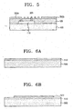
- FIG. 5 is a cross-sectional diagram for explaining a detailed structure of the inductor 300 shown in FIG. 4 .
- a predetermined-shaped metal line 110 is stacked on a top surface of a substrate 100, and a piezoelectric layer 120 is stacked on the top surface of the substrate 100 and includes the metal line 110.
- a predetermined-shaped metal layer 300 is stacked on the piezoelectric layer 120 to form the inductor 300 and the interconnection lines 350a and 350b.
- a portion of the metal layers 300 which are stacked as a coil shape serves to act as the inductor 300.
- the metal layer 300 also forms the interconnection lines 350 on the piezoelectric layer 120 which are connected to the external ground 400.
- One interconnection line 350a of the interconnection lines is electrically connected to the inductor 300 through the metal line 110 below the one interconnection line.
- an external device namely, the parallel FBAR 200
- the other interconnection line 350b is connected to the ground 400.
- the inductor 300 is serially connected to the parallel FBAR 200, so that an inductance (L) of the parallel FBAR 200 is increased by an amount of the natural inductance of the inductor 300.
- the natural inductance of the inductor 300 may be adjusted in response to the coil length, shape or the like, so that the frequency characteristic of the filter itself may be readily adjusted.
- the inductor 300 There is no air gap below the inductor 300 in FIG. 5 .
- a predetermined region of the substrate may be etched in order to isolate it from the substrate to thereby form the air gap.
- the air gap may be fabricated by fabricating a via hole in a lower portion of the substrate and injecting an etching solution or an etching gas through the via hole.
- the inductor 300 is connected to the parallel FBAR 200 in FIG. 5 , but there is a possibility of connecting the inductor to the serial FBAR when the filter is to be designed.
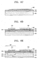
- FIGS. 6A to 6E are cross-sectional diagrams for explaining a process of fabricating the filter shown in FIG. 3 .
- a plurality of serial FBARs and a plurality of parallel FBARs are required to compose one filter, however, FIGS. 6A to 6E are cross-sectional diagrams illustrating one FBAR and an inductor for simplicity of description.
- an insulating layer 510 is first deposited on a top surface of a substrate 500.
- the insulating layer 510 serves to electrically isolate a metal portion from the substrate 500.
- Insulating materials such as SiO2 or Al2O2 may be employed for the material forming the insulating layer 510.
- a method for depositing the insulating layer 510 on the substrate 50 may include an RF magnetron sputtering method, an evaporation method or the like.
- a first electrode 520 is deposited on the insulating layer 510 and patterned to expose a predetermined region of the insulating layer 510.
- the first electrode 520 is formed using a typical conductive material such as a metal.
- a typical conductive material such as a metal.
- Al, W, Au, Pt, Ni, Ti, Cr, Pd, Mo or the like may be employed for the metal.
- a piezoelectric layer 530 is deposited on the top surfaces of the exposed insulating layer 510 and the first electrode 520 as shown in FIG. 6C .
- the piezoelectric layer 530 serves to generate a piezoelectric effect which converts electrical energy to mechanical energy such as an elastic wave as mentioned previously.
- AlN, ZnO or the like may be employed for forming the piezoelectric layer 530.
- a second electrode 540 is deposited and patterned on the piezoelectric layer 530.
- the second electrode 540 remaining on the piezoelectric layer 530 having the first electrode 520 positioned below the piezoelectric layer, forms a resonant portion 210.
- the second electrode 540 may remain on the piezoelectric layer 530 other than the portion where the resonant portion 210 is formed to thereby implement the inductor 300.
- the first electrode 520 serves to electrically connect the resonant portion 210 to the inductor 300.
- the interconnection line 350 to be connected to the ground may be implemented using the second electrode 540.
- the substrate below the resonant portion 210 may be etched to form the air gap 220.
- a via hole 230 which penetrates the upper portion or the lower portion of the substrate 500 may be formed in order to form the air gap 220.
- a packaging substrate 550 may be separately bonded in order to prevent contaminants from being introduced through the via hole 230 when the via hole is formed in the lower portion of the substrate 500.
- the bonding method may include a direct bonding method utilizing heating, an anodic bonding method utilizing a voltage, a bonding method utilizing an adhesive such as an epoxy, a eutectic bonding method utilizing a metal or the like.
- the bonding method utilizing the adhesive and the eutectic bonding method which are to be subjected to a low temperature step are preferably employed instead of the direct bonding method and the anodic bonding method which are subjected to a relatively high temperature step.
- Forming the air gap 220 leads to a final fabrication of the air gap type FBAR 200.
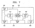
- FIG. 7 is a block diagram of a duplexer 600 fabricated using the filter shown in FIG. 3 in accordance with one embodiment of the present invention.
- the duplexer is a representative device which uses a band pass filter (hereinafter, it will be referred to as BPF).
- BPF band pass filter
- the duplexer according to one embodiment of the present invention includes a first BPF 610, a filter isolating portion 620, a second BPF 630, a first port 640, a second port 650, a third port 660, and a ground port 670.
- a filter implemented by combining a plurality of air gap type FBARs in a serial and parallel manner may be employed as each of the first and second BPF 610 and 630.
- Each filter may use a single chip filter formed on one substrate where the inductor is also formed to be included on the substrate.
- Each of the first to third ports 640, 650, and 660 may be electrically connected to an external device, and are formed of a conductive material. Each port is connected to one or more of the first and second BPFs 610 and 630 and the filter isolating portion 620 by means of the interconnection line 680 formed of a predetermined metal material.
- the ground port 670 shown in FIG. 7 means the portion which is electrically connected to an external ground terminal.
- the first port 640 serves to connect an external antenna (not shown) to the first BPF 610 and the filter isolating portion 620.
- the first BPF 610 is a receiving port filter and the second BPF 630 is a transmitting port filter, incoming signals are not applied to the second BPF 630 but are applied to the first BPF 610 because of the filter isolating portion 620.
- the filter isolating portion 620 may be implemented as the phase shifter combined with an inductor and capacitor as mentioned previously.
- the phase shifter causes the frequency phase difference between the receiving signal and the transmitting signal to be 90° to isolate the transmitting port filter from the receiving port filter.
- Each of the ports 640, 650, 660, 670, the interconnection line 680, the filter isolating portion 620 or the like may be fabricated together on one substrate using the fabrication process for the first and second BPFs 610 and 630.
- the same fabrication process as that shown in FIG. 6A to 6E may be employed. That is, after the insulating layer 510 is deposited on the top surface of the single substrate 500, the first electrode 520, the piezoelectric layer 530, and the second electrode 540 are concurrently stacked on the first BPF 610, the filter isolating portion 620, and the second BPF 630 in predetermined shapes, respectively.
- Each of the first BPF 610 and the second BPF 630 has the inductor 300 inside, respectively, so that each frequency characteristic is adjusted by the inductor 300. Accordingly, for each of FBARs composing the first BPF 610 and the second BPF 630, the electrode thickness or the like does not need to be adjusted, which leads to a simplified fabrication process and the decreased device volume because of the built-in inductor 300.
- a plurality of FBARs and inductors are formed on one substrate. Accordingly, a burdensome process may be avoided where each FBAR undergoes a different process for adjusting the frequency characteristic when the filter is fabricated.
- the inductors and the FBARs may be fabricated on one substrate so that the device may be small.
- a duplexer using the present filter may be fabricated. In this case, the filter having the built-in inductor and the filter isolating portion may be fabricated at the same time, so that a process of fabricating the duplexer may be simplified and the duplexer may be fabricated to be small.
Description
- The present invention relates generally to a filter using a film bulk acoustic resonator (hereinafter, it will be referred to as "FBAR"), a duplexer using the filter, and fabrication methods thereof. More particularly, the present invention relates to a filter which is fabricated by combining inductors for adjusting resonance characteristics with FBARs as a single chip in a serial and parallel manner, a duplexer using the filter, and fabrication methods thereof.
- In recent years, demand for mobile communication devices such as cellular phones is rapidly increasing, so that demand for a small-sized and light-weight filter and a duplexer used in such mobile communication devices is also increasing. In the meantime, the FBAR is known to be suitable for a small and light-weight filter. The FBAR has advantages in that it allows mass production at a minimum cost and allows the minimum size implementation. In addition, it has advantages in that it may implement a high quality factor Q which is a main characteristic of the filter, it may be utilized in a microwave band, and in particular it may also be utilized in a personal communication system (PCS) band and a digital cordless system (DCS) band.
- In general, the FBAR device includes a resonant portion on a substrate where a bottom electrode, a piezoelectric layer, and a top electrode are sequentially stacked. The operating principle of the FBAR is as follows. Electrical energy is applied to the electrode to induce a time-varying magnetic field within the piezoelectric layer, and the magnetic field induces a bulk acoustic wave in the same direction as the vibration direction of the resonant portion within the piezoelectric layer to thereby generate a resonance.
- A ladder type filter is one type of filter that uses the FBAR device. The ladder type filter is a band pass filter, wherein a plurality of FBAR devices is combined in a serial and parallel manner to adjust resonance characteristics of each device to thereby pass only signals within a predetermined frequency band.
-
FIG. 1 is a block diagram illustrating a ladder type filter where a plurality of thin film resonators (TFRs) is combined in a serial and parallel manner as disclosed inU.S. Patent No. 6,377,136 . Referring toFIG. 1 , the filter includes a plurality of serial TFRs S1, S2,...,SN, and a plurality of parallel TFRs P1, P2,..., Pn. Each of theserial TFRs parallel TFRs serial TFRs -
FIG. 2 is a graph illustrating impedance characteristics of serial and parallel TFRs included in the ladder type filter. Referring toFIG. 2 , f1 and f2 of the impedancecharacteristic graph 30 of the serial TFR indicate antiresonance frequency and resonance frequency, respectively, and f3 and f4 of the impedancecharacteristic graph 40 of the parallel TFR indicate antiresonance frequency and resonance frequency, respectively. When the frequency characteristic of the parallel TFR or the serial TFR is adjusted so as to match the antiresonance frequency f3 of the parallel TFR with the resonance frequency f2 of the serial TFR, only signals within the frequency band ranging from f1 to f4 are passed, which is the operation of the band pass filter. In this case, the resonance frequency of the band pass filter is f2 which is equal to f3. - In order to adjust the frequency characteristic of the serial TFR or the parallel TFR in the filter shown in
FIG. 1 , thickness and material for electrode, piezoelectric layer or the like which compose each of the TFRs should be fabricated to be different from one another. As a result, there occurs a difficulty in having fabrication processes different from one another per each of TFRs. - Alternatively, the frequency characteristic of the band pass filter may be adjusted by properly combining the TFRs having uniform frequency characteristics and connecting devices such as inductors to the parallel TFR. However, the connection of an external device such as inductor causes the device volume to be increased. As a result, it is difficult to apply it to a small-sized communication apparatus such as a cellular phone.
- Such a filter may be employed in a device such as a duplexer. The duplexer is a device for transceiving signals through one antenna, and has a structure including a transmitting port filter, a receiving port filter, and a filter isolating portion for preventing signal interference between the filters. The transmitting port filter filters only signals to be transmitted outward through the antenna, and the receiving port filter filters only signals to be received from outside the duplexer. The filter isolating portion may be implemented as a phase shifter which serves to prevent interference between the filters by having a phase difference of 90° between the frequency of the transmitting signal and that of the receiving signal. The phase shifter may be implemented typically using a capacitor and an inductor.
- The duplexer also uses the filter, which in turn causes the size of the duplexer to be increased in response to the increased size of the fabricated filter. In addition, when the filter fabrication process becomes complicated, it becomes more difficult to fabricate the duplexer.
- Document
EP 1058383 discloses a band-pass filter comprising shunt elements and series elements in which the series elements and the shunt elements are connected to form a ladder circuit, and each of the elements includes a film bulk acoustic resonator. An FBAR-based duplexer comprises a first port, a second port, a third port, a first FBAR-based band-pass filter connected between the first port and the third port and a series circuit connected between the second port and the third port. The series circuit includes a 90 DEG phase shifter in series with a second FBAR-based band-pass filter. - According to one aspect of the present invention, there is provided a filter, which includes a substrate on which a first port, a second port, and a ground port are formed to be connected to an external terminal; at least one first film bulk acoustic resonator serially connecting the first port to the second port on the substrate; at least one second film bulk acoustic resonator parallel connected to an interconnection node formed between the first port and the second port; and at least one inductor serially connecting the second film bulk acoustic resonator to the ground port.
- In this case, at least one of the first and second film bulk acoustic resonators includes a cavity formed in a predetermined region of the substrate; and a resonant portion composed of a first electrode, a piezoelectric layer, and a second electrode which are sequentially stacked in an upper space spaced from a bottom surface of the cavity by a predetermined distance.
- The inductor also includes a piezoelectric layer stacked on an upper surface of the substrate except the region where the empty region is formed; a metal layer stacked on the top surface of the piezoelectric layer as a predetermined coil shape; and an interconnection line for electrically connecting the metal layer to the second film bulk acoustic resonator.
- According to another aspect of the present invention, there is provided a duplexer, which includes a first filter having at least one first inductor and filtering a signal within a predetermined receiving frequency band tuned by the first inductor; a second filter having at least one second inductor and filtering a signal within a predetermined receiving frequency band tuned by the second inductor; and a filter isolating portion formed between the first filter and the second filter to prevent a signal from flowing between the first filter and the second filter, wherein at least one of the first and second filters are as claimed in
claim 1. - Preferably, but not necessarily, the duplexer may further include a substrate where a first port, a second port, and a third port are formed to be electrically connected to an external terminal. Accordingly, the second port and the third port are preferably connected to the first filter and the second filter, respectively, and the first port is preferably connected to the first filter and the filter isolating portion, and the filter isolating portion is preferably connected between the first port and the second filter.
- According to another aspect of the present invention, there is provided a method for fabricating a filter, which includes (a) stacking a predetermined insulating layer on a top surface of a substrate; (b) depositing a first metal layer on the insulating layer and patterning it to form a plurality of first electrodes; (c) stacking a piezoelectric layer on top surfaces of the plurality of the first electrodes and the insulating layer; (d) depositing a second metal layer on the piezoelectric layer and patterning it to form a plurality of second electrodes and a predetermined coil-shaped inductor; and (e) etching the substrate below the region where the first electrode, the piezoelectric layer, and the second electrode are sequentially stacked to form an air gap to form a plurality of resultant film bulk acoustic resonators.
- In this case, the (e) step of etching the substrate preferably, but not necessarily, includes forming at least one via hole penetrating a predetermined region of a lower portion of the substrate; using the via hole to etch the substrate below the region; and bonding a predetermined packaging substrate to the substrate to shield the via hole.
- The invention thus provides a filter which may be implemented as a small-sized filter by fabricating inductors and FBARs as one body through a simplified fabrication process, and the invention also provides a duplexer using the filter, and fabrication methods thereof.
- The above aspects and features of the present invention will be more apparent by describing certain embodiments of the present invention with reference to the accompanying drawings, in which:
-
FIG. 1 is a block diagram illustrating a ladder type filter fabricated by combining FBARs in the related art; -
FIG. 2 is a graph illustrating impedance characteristics of FBARs composing a ladder type filter; -
FIG. 3 is a block diagram illustrating a filter in accordance with one embodiment of the present invention; -
FIG. 4 is a schematic diagram illustrating a FBAR and an inductor composing the filter shownFIG. 3 ; -
FIG. 5 is a cross-sectional diagram illustrating a detailed structure of the inductor shown inFIG. 4 ; -
FIGS. 6A to 6E are cross-sectional diagrams for explaining a process of fabricating the filter shown inFIG. 3 ; and -
FIG. 7 is a block diagram illustrating a duplexer using a filter in accordance with one embodiment of the present invention. - Hereinafter, the present invention will be described in detail with reference to illustrative accompanying drawings.
-
FIG. 3 is a block diagram of a filter which is combined with a plurality of film bulk acoustic resonators (FBARs) in accordance with one embodiment of the present invention. Referring toFIG. 3 , the filter includes a plurality of serial FBARs 110, 120,..., M such as FBAR S1, S2,...,SM, a plurality ofparallel FBARs inductors parallel FBARs FIG. 2 . - An air gap type FBAR may be employed for the serial and parallel FBARs, which includes a resonant portion where a bottom electrode, a piezoelectric layer, and a top electrode are sequentially stacked on a substrate, and an air gap positioned below the resonant portion.
-
Inductors Serial FBARs parallel FBARs inductors FIG. 3 . Accordingly, the fabrication process for each FBAR may still be used to implement the inductor. That is, the inductor may be fabricated by patterning the top electrode or the bottom electrode as a predetermined coil shape during the deposition and patterning of the top electrode or the bottom electrode. In addition, a piezoelectric layer may be used as an insulating layer for insulating the inductor from the substrate. As shown inFIG. 3 , theparallel FBARs -
FIG. 4 is a cross-sectional diagram illustrating a portion where aninductor 300 connects oneparallel FBAR 200 to aground 400. Theinductor 300 is fabricated on the same substrate as theparallel FBAR 200 to be implemented on a single chip. Theinductor 300 connects theparallel FBAR 200 to theground 400 throughinterconnection lines -
FIG. 5 is a cross-sectional diagram for explaining a detailed structure of theinductor 300 shown inFIG. 4 . Referring toFIG. 5 , a predetermined-shapedmetal line 110 is stacked on a top surface of asubstrate 100, and apiezoelectric layer 120 is stacked on the top surface of thesubstrate 100 and includes themetal line 110. A predetermined-shapedmetal layer 300 is stacked on thepiezoelectric layer 120 to form theinductor 300 and theinterconnection lines inductor 300. Themetal layer 300 also forms the interconnection lines 350 on thepiezoelectric layer 120 which are connected to theexternal ground 400. Oneinterconnection line 350a of the interconnection lines is electrically connected to theinductor 300 through themetal line 110 below the one interconnection line. As a result, an external device, namely, theparallel FBAR 200, is electrically connected to theinductor 300. Theother interconnection line 350b is connected to theground 400. As shown inFIG. 5 , theinductor 300 is serially connected to theparallel FBAR 200, so that an inductance (L) of theparallel FBAR 200 is increased by an amount of the natural inductance of theinductor 300. The natural inductance of theinductor 300 may be adjusted in response to the coil length, shape or the like, so that the frequency characteristic of the filter itself may be readily adjusted. - There is no air gap below the
inductor 300 inFIG. 5 . However, a predetermined region of the substrate may be etched in order to isolate it from the substrate to thereby form the air gap. In this case, the air gap may be fabricated by fabricating a via hole in a lower portion of the substrate and injecting an etching solution or an etching gas through the via hole. Theinductor 300 is connected to theparallel FBAR 200 inFIG. 5 , but there is a possibility of connecting the inductor to the serial FBAR when the filter is to be designed. -
FIGS. 6A to 6E are cross-sectional diagrams for explaining a process of fabricating the filter shown inFIG. 3 . As mentioned previously, a plurality of serial FBARs and a plurality of parallel FBARs are required to compose one filter, however,FIGS. 6A to 6E are cross-sectional diagrams illustrating one FBAR and an inductor for simplicity of description. - Referring to
FIG. 6A , an insulatinglayer 510 is first deposited on a top surface of asubstrate 500. The insulatinglayer 510 serves to electrically isolate a metal portion from thesubstrate 500. Insulating materials such as SiO2 or Al2O2 may be employed for the material forming the insulatinglayer 510. A method for depositing the insulatinglayer 510 on the substrate 50 may include an RF magnetron sputtering method, an evaporation method or the like. - Next, as shown in
FIG. 6B , afirst electrode 520 is deposited on the insulatinglayer 510 and patterned to expose a predetermined region of the insulatinglayer 510. Thefirst electrode 520 is formed using a typical conductive material such as a metal. In particular, Al, W, Au, Pt, Ni, Ti, Cr, Pd, Mo or the like may be employed for the metal. - A
piezoelectric layer 530 is deposited on the top surfaces of the exposed insulatinglayer 510 and thefirst electrode 520 as shown inFIG. 6C . Thepiezoelectric layer 530 serves to generate a piezoelectric effect which converts electrical energy to mechanical energy such as an elastic wave as mentioned previously. AlN, ZnO or the like may be employed for forming thepiezoelectric layer 530. - As shown in
FIG. 6D , asecond electrode 540 is deposited and patterned on thepiezoelectric layer 530. In this case, along with thefirst electrode 520 and thepiezoelectric layer 530, thesecond electrode 540 remaining on thepiezoelectric layer 530 having thefirst electrode 520 positioned below the piezoelectric layer, forms aresonant portion 210. Thesecond electrode 540 may remain on thepiezoelectric layer 530 other than the portion where theresonant portion 210 is formed to thereby implement theinductor 300. Thefirst electrode 520 serves to electrically connect theresonant portion 210 to theinductor 300. The interconnection line 350 to be connected to the ground may be implemented using thesecond electrode 540. - As shown in
FIG. 6E , the substrate below theresonant portion 210 may be etched to form theair gap 220. In this case, a viahole 230 which penetrates the upper portion or the lower portion of thesubstrate 500 may be formed in order to form theair gap 220. Apackaging substrate 550 may be separately bonded in order to prevent contaminants from being introduced through the viahole 230 when the via hole is formed in the lower portion of thesubstrate 500. The bonding method may include a direct bonding method utilizing heating, an anodic bonding method utilizing a voltage, a bonding method utilizing an adhesive such as an epoxy, a eutectic bonding method utilizing a metal or the like. However, the bonding method utilizing the adhesive and the eutectic bonding method which are to be subjected to a low temperature step are preferably employed instead of the direct bonding method and the anodic bonding method which are subjected to a relatively high temperature step. - Forming the
air gap 220 leads to a final fabrication of the airgap type FBAR 200. Alternatively, it is also possible to etch the substrate region below theinductor 300 to thereby form the air gap. -
FIG. 7 is a block diagram of aduplexer 600 fabricated using the filter shown inFIG. 3 in accordance with one embodiment of the present invention. As mentioned previously, the duplexer is a representative device which uses a band pass filter (hereinafter, it will be referred to as BPF). Referring toFIG. 7 , the duplexer according to one embodiment of the present invention includes afirst BPF 610, afilter isolating portion 620, asecond BPF 630, afirst port 640, asecond port 650, athird port 660, and aground port 670. - A filter implemented by combining a plurality of air gap type FBARs in a serial and parallel manner may be employed as each of the first and
second BPF - Each of the first to
third ports filter isolating portion 620 by means of theinterconnection line 680 formed of a predetermined metal material. - The
ground port 670 shown inFIG. 7 means the portion which is electrically connected to an external ground terminal. - Referring to
FIG. 7 , thefirst port 640 serves to connect an external antenna (not shown) to thefirst BPF 610 and thefilter isolating portion 620. When thefirst BPF 610 is a receiving port filter and thesecond BPF 630 is a transmitting port filter, incoming signals are not applied to thesecond BPF 630 but are applied to thefirst BPF 610 because of thefilter isolating portion 620. - The
filter isolating portion 620 may be implemented as the phase shifter combined with an inductor and capacitor as mentioned previously. The phase shifter causes the frequency phase difference between the receiving signal and the transmitting signal to be 90° to isolate the transmitting port filter from the receiving port filter. - Each of the
ports interconnection line 680, thefilter isolating portion 620 or the like may be fabricated together on one substrate using the fabrication process for the first and second BPFs 610 and 630. The same fabrication process as that shown inFIG. 6A to 6E may be employed. That is, after the insulatinglayer 510 is deposited on the top surface of thesingle substrate 500, thefirst electrode 520, thepiezoelectric layer 530, and thesecond electrode 540 are concurrently stacked on thefirst BPF 610, thefilter isolating portion 620, and thesecond BPF 630 in predetermined shapes, respectively. Each of thefirst BPF 610 and thesecond BPF 630 has theinductor 300 inside, respectively, so that each frequency characteristic is adjusted by theinductor 300. Accordingly, for each of FBARs composing thefirst BPF 610 and thesecond BPF 630, the electrode thickness or the like does not need to be adjusted, which leads to a simplified fabrication process and the decreased device volume because of the built-ininductor 300. - As mentioned above, in the filter according to an embodiment of the present invention, a plurality of FBARs and inductors are formed on one substrate. Accordingly, a burdensome process may be avoided where each FBAR undergoes a different process for adjusting the frequency characteristic when the filter is fabricated. In addition, the inductors and the FBARs may be fabricated on one substrate so that the device may be small. Furthermore, a duplexer using the present filter may be fabricated. In this case, the filter having the built-in inductor and the filter isolating portion may be fabricated at the same time, so that a process of fabricating the duplexer may be simplified and the duplexer may be fabricated to be small.
- The foregoing embodiment and advantages are merely exemplary and are not to be construed as limiting the present invention. The present teaching can be readily applied to other types of apparatuses. Also, the description of the embodiments of the present invention is intended to be illustrative, and not to limit the scope of the claims, and many alternatives, modifications, and variations will be apparent to those skilled in the art.
Claims (6)
- A filter comprising:a substrate (100;500) on which a first port (640), a second port (650), and a ground port (670) are formed to be connected to an external terminal;at least one first film bulk acoustic resonator (110,120) serially connecting the first port (640) to the second port (650) on the substrate;at least one second film bulk acoustic resonator (210,220) parallel connected to an interconnection node formed between the first port and the second port; andat least one inductor (310,320) serially connecting the second film bulk acoustic resonator (210,220) to the ground port, wherein at least one of the first and second film bulk acoustic resonators includes:characterised in that the inductor (310,320) comprises:a cavity (220) formed in a predetermined region of the substrate (100;500); anda resonant portion comprising a first electrode (520), a piezoelectric layer (530), and a second electrode (540), which are sequentially stacked in an upper space spaced from a bottom surface of the cavity (220) by a predetermined distance,the piezoelectric layer (530) stacked on an upper surface of the substrate away from the predetermined region where the cavity region is formed;a metal layer (400) stacked on the top surface of the piezoelectric layer as a predetermined coil shape; andan interconnection line for electrically connecting the metal layer (400) to the second film bulk acoustic resonator (200;630).
- A duplexer comprising:a first filter (610) having at least one first inductor and filtering a signal within a predetermined receiving frequency band tuned by the first inductor;a second filter (620) having at least one second inductor and filtering a signal within a predetermined receiving frequency band tuned by the second inductor; anda filter isolating portion (620) formed between the first filter and the second filter to prevent a signal from flowing between the first filter and the second filter,wherein at least one of the first and second filters are as claimed in claim 1.
- The duplexer as recited in claim 2, wherein a third port (660) on the substrate is formed to be electrically connected to an external terminal,
wherein the second port (650) and the third port (660) are connected to the first filter (610) and the second filter (630), respectively, and the first port (640) is connected to the first filter (610) and the filter isolating portion (620), and the filter isolating portion (620) is connected between the first port (640) and the second filter (630). - The duplexer as recited in claim 2 or 3, wherein the filter isolating portion is implemented to have at least one capacitor combined with a coil, and makes a frequency phase difference of signals filtered in the first and second filters to be 90°.
- A method for fabricating a filter comprising:(a) stacking a predetermined insulating layer (510) on a top surface of a substrate (500);(b) depositing a first metal layer (520) on the insulating layer and patterning the first metal layer to form a plurality of first electrodes;(c) stacking a piezoelectric layer (530) on top surfaces of the plurality of the first electrodes and the insulating layer (510);(d) depositing a second metal layer (540) on the piezoelectric layer and patterning the second metal layer to form a plurality of second electrodes and a predetermined coil-shaped inductor (300); and(e) etching the substrate below respective regions where a respective one of the plurality of the first electrodes, the piezoelectric layer, and a respective one of the plurality of the second electrodes are sequentially stacked to form an air gap (220) to form a plurality of resultant film bulk acoustic resonators.
- The method as recited in claim 5, wherein the etching of substrate comprises:forming at least one via hole (230) penetrating a predetermined region of a lower portion of the substrate;using the via hole (230) to etch the substrate below the predetermined region; andbonding a predetermined packaging substrate (550) to the substrate to shield the via hole.
Applications Claiming Priority (2)
| Application Number | Priority Date | Filing Date | Title |
|---|---|---|---|
| KR20040034970A KR100635268B1 (en) | 2004-05-17 | 2004-05-17 | Filter comprising inductor, duplexer using the filter and fabricating methods thereof |
| KR2004034970 | 2004-05-17 |
Publications (3)
| Publication Number | Publication Date |
|---|---|
| EP1598934A2 EP1598934A2 (en) | 2005-11-23 |
| EP1598934A3 EP1598934A3 (en) | 2007-11-14 |
| EP1598934B1 true EP1598934B1 (en) | 2013-11-06 |
Family
ID=34941329
Family Applications (1)
| Application Number | Title | Priority Date | Filing Date |
|---|---|---|---|
| EP20050253005 Active EP1598934B1 (en) | 2004-05-17 | 2005-05-17 | Filter comprising thin-film resonators and inductor, duplexer and fabricating methods thereof |
Country Status (4)
| Country | Link |
|---|---|
| US (1) | US7250831B2 (en) |
| EP (1) | EP1598934B1 (en) |
| JP (1) | JP2005333644A (en) |
| KR (1) | KR100635268B1 (en) |
Families Citing this family (19)
| Publication number | Priority date | Publication date | Assignee | Title |
|---|---|---|---|---|
| KR100565799B1 (en) * | 2003-12-22 | 2006-03-29 | 삼성전자주식회사 | Duplexer fabricated with monolithic FBAR and Isolation part and the method thereof |
| KR100631216B1 (en) * | 2004-05-17 | 2006-10-04 | 삼성전자주식회사 | Air gap type FBAR and fabricating method thereof |
| KR100750736B1 (en) * | 2004-11-10 | 2007-08-22 | 삼성전자주식회사 | Filter comprising one trimming inductor |
| US7562429B2 (en) | 2005-06-20 | 2009-07-21 | Avago Technologies General Ip (Singapore) Pte. Ltd. | Suspended device and method of making |
| JP4791181B2 (en) * | 2005-12-28 | 2011-10-12 | 京セラ株式会社 | Thin film bulk acoustic wave resonator, filter and communication device including the same, and method for manufacturing thin film bulk acoustic wave resonator |
| JP2007259296A (en) | 2006-03-24 | 2007-10-04 | Toshiba Corp | Antenna duplexer and mobile phone |
| US7851333B2 (en) * | 2007-03-15 | 2010-12-14 | Infineon Technologies Ag | Apparatus comprising a device and method for producing it |
| US8291559B2 (en) * | 2009-02-24 | 2012-10-23 | Epcos Ag | Process for adapting resonance frequency of a BAW resonator |
| KR101719325B1 (en) * | 2010-07-19 | 2017-03-23 | 삼성전자주식회사 | Rf filter and rf duplexer of balanced structure using bulk acoustic wave resonator |
| DE102011100468B4 (en) * | 2011-05-04 | 2013-07-04 | Epcos Ag | Bulk Acoustic Wave BAW filter, method of fabrication and duplexer |
| WO2013026056A1 (en) * | 2011-08-18 | 2013-02-21 | Northeastern University | Electrostatically tunable magnetoelectric inductors with large inductance tunability |
| US20140055214A1 (en) * | 2012-03-19 | 2014-02-27 | Qualcomm Incorporated | Multi-mode bandpass filter |
| KR101644380B1 (en) * | 2012-08-30 | 2016-08-01 | 가부시키가이샤 무라타 세이사쿠쇼 | Acoustic wave filter device and duplexer |
| CN108781065B (en) * | 2016-03-08 | 2022-05-17 | 株式会社村田制作所 | Elastic wave device |
| KR101861271B1 (en) * | 2016-10-31 | 2018-05-28 | 삼성전기주식회사 | Filter including acoustic wave resonator |
| CN108091982B (en) * | 2017-12-28 | 2019-11-15 | 中国电子科技集团公司第二十六研究所 | Micro-nano film magnetosonic antenna |
| CN113612463B (en) * | 2021-06-30 | 2023-07-21 | 中国电子科技集团公司第十三研究所 | Ladder type thin film bulk acoustic resonator filter and filter assembly |
| CN113644893B (en) * | 2021-06-30 | 2023-07-25 | 中国电子科技集团公司第十三研究所 | Bulk acoustic wave filter and filter assembly |
| CN114157267B (en) * | 2022-02-08 | 2022-05-20 | 深圳新声半导体有限公司 | Packaging structure of bulk acoustic wave filter chip |
Family Cites Families (20)
| Publication number | Priority date | Publication date | Assignee | Title |
|---|---|---|---|---|
| JP3378151B2 (en) | 1996-09-17 | 2003-02-17 | 沖電気工業株式会社 | Surface acoustic wave filter circuit |
| US6262637B1 (en) * | 1999-06-02 | 2001-07-17 | Agilent Technologies, Inc. | Duplexer incorporating thin-film bulk acoustic resonators (FBARs) |
| DE19962028A1 (en) * | 1999-12-22 | 2001-06-28 | Philips Corp Intellectual Pty | Filter arrangement |
| US6407649B1 (en) * | 2001-01-05 | 2002-06-18 | Nokia Corporation | Monolithic FBAR duplexer and method of making the same |
| JP2002314372A (en) | 2001-02-07 | 2002-10-25 | Murata Mfg Co Ltd | Surface acoustic wave filter device |
| US6885260B2 (en) * | 2001-05-11 | 2005-04-26 | Ube Industries, Ltd. | Filter using film bulk acoustic resonator and transmission/reception switch |
| US6710681B2 (en) | 2001-07-13 | 2004-03-23 | Agilent Technologies, Inc. | Thin film bulk acoustic resonator (FBAR) and inductor on a monolithic substrate and method of fabricating the same |
| US6670866B2 (en) * | 2002-01-09 | 2003-12-30 | Nokia Corporation | Bulk acoustic wave resonator with two piezoelectric layers as balun in filters and duplexers |
| TW540173B (en) * | 2002-05-03 | 2003-07-01 | Asia Pacific Microsystems Inc | Bulk acoustic device having integrated fine-tuning and trimming devices |
| DE10225202B4 (en) * | 2002-06-06 | 2017-06-01 | Epcos Ag | With acoustic waves working device with a matching network |
| JP2004112277A (en) | 2002-09-18 | 2004-04-08 | Murata Mfg Co Ltd | Piezoelectric thin-film filter, branching filter, and communication machine |
| JP2004173234A (en) * | 2002-11-08 | 2004-06-17 | Murata Mfg Co Ltd | Branching filter and combination module |
| KR100486627B1 (en) * | 2003-02-21 | 2005-05-03 | 엘지전자 주식회사 | Semiconductor package |
| KR100517841B1 (en) * | 2003-02-22 | 2005-09-30 | 주식회사 엠에스솔루션 | FBAR band pass filter, Duplexer having the FBAR band pass filter and Methods for manufacturing the same |
| KR100555762B1 (en) * | 2003-10-07 | 2006-03-03 | 삼성전자주식회사 | Air-gap type ???? fabrication method and FBAR fabricated by the same, filter and duPlexer using the FBAR. |
| KR20050035904A (en) * | 2003-10-07 | 2005-04-20 | 삼성전기주식회사 | Bulk acoustic wave filter of ladder type with the common ground inductor |
| EP1533897A3 (en) * | 2003-11-20 | 2010-06-30 | Panasonic Corporation | Filter using piezoelectric resonator |
| KR100565799B1 (en) * | 2003-12-22 | 2006-03-29 | 삼성전자주식회사 | Duplexer fabricated with monolithic FBAR and Isolation part and the method thereof |
| US7057477B2 (en) * | 2003-12-24 | 2006-06-06 | Intel Corporation | Integration of FBAR filter(s) and on-chip inductors |
| KR100750736B1 (en) * | 2004-11-10 | 2007-08-22 | 삼성전자주식회사 | Filter comprising one trimming inductor |
-
2004
- 2004-05-17 KR KR20040034970A patent/KR100635268B1/en active IP Right Grant
-
2005
- 2005-05-17 JP JP2005144411A patent/JP2005333644A/en active Pending
- 2005-05-17 EP EP20050253005 patent/EP1598934B1/en active Active
- 2005-05-17 US US11/130,156 patent/US7250831B2/en active Active
Also Published As
| Publication number | Publication date |
|---|---|
| KR20050109871A (en) | 2005-11-22 |
| EP1598934A2 (en) | 2005-11-23 |
| JP2005333644A (en) | 2005-12-02 |
| EP1598934A3 (en) | 2007-11-14 |
| US20050253668A1 (en) | 2005-11-17 |
| US7250831B2 (en) | 2007-07-31 |
| KR100635268B1 (en) | 2006-10-19 |
Similar Documents
| Publication | Publication Date | Title |
|---|---|---|
| EP1598934B1 (en) | Filter comprising thin-film resonators and inductor, duplexer and fabricating methods thereof | |
| EP1469599B1 (en) | Air gap type FBAR, duplexer using the FBAR, and fabricating methods thereof | |
| CN100511998C (en) | Coupled BAW resonator based duplexers | |
| KR100743555B1 (en) | Transmitter filter arrangement for multiband mobile phone | |
| KR100565799B1 (en) | Duplexer fabricated with monolithic FBAR and Isolation part and the method thereof | |
| JP4316557B2 (en) | Monolithic duplexer and method for manufacturing the same | |
| US20040164367A1 (en) | Duplexer filter having film bulk acoustic resonator and semiconductor package thereof | |
| WO2003058809A2 (en) | Bulk acoustic wave resonator with two piezoelectric layers as balun in filters and duplexers | |
| JP2003347884A (en) | Film bulk acoustic resonator element and manufacturing method thereof | |
| WO2004066490A2 (en) | Resonator filter structure having equal resonance frequencies | |
| CN108023561A (en) | Wave filter including bulk acoustic wave resonator | |
| KR100555762B1 (en) | Air-gap type ???? fabrication method and FBAR fabricated by the same, filter and duPlexer using the FBAR. | |
| KR100425685B1 (en) | Manufacturing method for duplexer and bandpass filter using thinfilm bulk acoustic resonator |
Legal Events
| Date | Code | Title | Description |
|---|---|---|---|
| PUAI | Public reference made under article 153(3) epc to a published international application that has entered the european phase |
Free format text: ORIGINAL CODE: 0009012 |
|
| AK | Designated contracting states |
Kind code of ref document: A2 Designated state(s): AT BE BG CH CY CZ DE DK EE ES FI FR GB GR HU IE IS IT LI LT LU MC NL PL PT RO SE SI SK TR |
|
| AX | Request for extension of the european patent |
Extension state: AL BA HR LV MK YU |
|
| RIN1 | Information on inventor provided before grant (corrected) |
Inventor name: HONG, SEOG-WOO Inventor name: PARK, HAE-SEOK Inventor name: KIM, JONG-SEOK Inventor name: NAM, KUANG-WOO Inventor name: PARK, YUN-KWON Inventor name: KIM, DUCK-HWAN Inventor name: SONG, IN-SANG Inventor name: HA, BYEOUNG-JU |
|
| PUAL | Search report despatched |
Free format text: ORIGINAL CODE: 0009013 |
|
| AK | Designated contracting states |
Kind code of ref document: A3 Designated state(s): AT BE BG CH CY CZ DE DK EE ES FI FR GB GR HU IE IS IT LI LT LU MC NL PL PT RO SE SI SK TR |
|
| AX | Request for extension of the european patent |
Extension state: AL BA HR LV MK YU |
|
| 17P | Request for examination filed |
Effective date: 20080220 |
|
| 17Q | First examination report despatched |
Effective date: 20080317 |
|
| AKX | Designation fees paid |
Designated state(s): DE FI FR GB SE |
|
| RAP1 | Party data changed (applicant data changed or rights of an application transferred) |
Owner name: SAMSUNG ELECTRONICS CO., LTD. |
|
| GRAP | Despatch of communication of intention to grant a patent |
Free format text: ORIGINAL CODE: EPIDOSNIGR1 |
|
| INTG | Intention to grant announced |
Effective date: 20130606 |
|
| GRAS | Grant fee paid |
Free format text: ORIGINAL CODE: EPIDOSNIGR3 |
|
| GRAA | (expected) grant |
Free format text: ORIGINAL CODE: 0009210 |
|
| AK | Designated contracting states |
Kind code of ref document: B1 Designated state(s): DE FI FR GB SE |
|
| REG | Reference to a national code |
Ref country code: GB Ref legal event code: FG4D |
|
| REG | Reference to a national code |
Ref country code: DE Ref legal event code: R096 Ref document number: 602005041736 Country of ref document: DE Effective date: 20140102 |
|
| PG25 | Lapsed in a contracting state [announced via postgrant information from national office to epo] |
Ref country code: FI Free format text: LAPSE BECAUSE OF FAILURE TO SUBMIT A TRANSLATION OF THE DESCRIPTION OR TO PAY THE FEE WITHIN THE PRESCRIBED TIME-LIMIT Effective date: 20131106 Ref country code: SE Free format text: LAPSE BECAUSE OF FAILURE TO SUBMIT A TRANSLATION OF THE DESCRIPTION OR TO PAY THE FEE WITHIN THE PRESCRIBED TIME-LIMIT Effective date: 20131106 |
|
| REG | Reference to a national code |
Ref country code: DE Ref legal event code: R097 Ref document number: 602005041736 Country of ref document: DE |
|
| PLBE | No opposition filed within time limit |
Free format text: ORIGINAL CODE: 0009261 |
|
| STAA | Information on the status of an ep patent application or granted ep patent |
Free format text: STATUS: NO OPPOSITION FILED WITHIN TIME LIMIT |
|
| 26N | No opposition filed |
Effective date: 20140807 |
|
| REG | Reference to a national code |
Ref country code: DE Ref legal event code: R097 Ref document number: 602005041736 Country of ref document: DE Effective date: 20140807 |
|
| REG | Reference to a national code |
Ref country code: FR Ref legal event code: PLFP Year of fee payment: 12 |
|
| REG | Reference to a national code |
Ref country code: FR Ref legal event code: PLFP Year of fee payment: 13 |
|
| REG | Reference to a national code |
Ref country code: FR Ref legal event code: PLFP Year of fee payment: 14 |
|
| P01 | Opt-out of the competence of the unified patent court (upc) registered |
Effective date: 20230530 |
|
| PGFP | Annual fee paid to national office [announced via postgrant information from national office to epo] |
Ref country code: FR Payment date: 20230421 Year of fee payment: 19 Ref country code: DE Payment date: 20230425 Year of fee payment: 19 |
|
| PGFP | Annual fee paid to national office [announced via postgrant information from national office to epo] |
Ref country code: GB Payment date: 20230420 Year of fee payment: 19 |