EP3501162B1 - Fangverbinder für betätigte verriegelungsvorrichtungen - Google Patents
Fangverbinder für betätigte verriegelungsvorrichtungen Download PDFInfo
- Publication number
- EP3501162B1 EP3501162B1 EP17761356.9A EP17761356A EP3501162B1 EP 3501162 B1 EP3501162 B1 EP 3501162B1 EP 17761356 A EP17761356 A EP 17761356A EP 3501162 B1 EP3501162 B1 EP 3501162B1
- Authority
- EP
- European Patent Office
- Prior art keywords
- contact
- locking
- termination
- contact surface
- wire
- Prior art date
- Legal status (The legal status is an assumption and is not a legal conclusion. Google has not performed a legal analysis and makes no representation as to the accuracy of the status listed.)
- Active
Links
Images





Classifications
-
- G—PHYSICS
- G06—COMPUTING OR CALCULATING; COUNTING
- G06F—ELECTRIC DIGITAL DATA PROCESSING
- G06F1/00—Details not covered by groups G06F3/00 - G06F13/00 and G06F21/00
- G06F1/16—Constructional details or arrangements
- G06F1/1613—Constructional details or arrangements for portable computers
- G06F1/1633—Constructional details or arrangements of portable computers not specific to the type of enclosures covered by groups G06F1/1615 - G06F1/1626
- G06F1/1675—Miscellaneous details related to the relative movement between the different enclosures or enclosure parts
- G06F1/1679—Miscellaneous details related to the relative movement between the different enclosures or enclosure parts for locking or maintaining the movable parts of the enclosure in a fixed position, e.g. latching mechanism at the edge of the display in a laptop or for the screen protective cover of a PDA
-
- F—MECHANICAL ENGINEERING; LIGHTING; HEATING; WEAPONS; BLASTING
- F03—MACHINES OR ENGINES FOR LIQUIDS; WIND, SPRING, OR WEIGHT MOTORS; PRODUCING MECHANICAL POWER OR A REACTIVE PROPULSIVE THRUST, NOT OTHERWISE PROVIDED FOR
- F03G—SPRING, WEIGHT, INERTIA OR LIKE MOTORS; MECHANICAL-POWER PRODUCING DEVICES OR MECHANISMS, NOT OTHERWISE PROVIDED FOR OR USING ENERGY SOURCES NOT OTHERWISE PROVIDED FOR
- F03G7/00—Mechanical-power-producing mechanisms, not otherwise provided for or using energy sources not otherwise provided for
- F03G7/06—Mechanical-power-producing mechanisms, not otherwise provided for or using energy sources not otherwise provided for using expansion or contraction of bodies due to heating, cooling, moistening, drying or the like
- F03G7/061—Mechanical-power-producing mechanisms, not otherwise provided for or using energy sources not otherwise provided for using expansion or contraction of bodies due to heating, cooling, moistening, drying or the like characterised by the actuating element
- F03G7/0614—Mechanical-power-producing mechanisms, not otherwise provided for or using energy sources not otherwise provided for using expansion or contraction of bodies due to heating, cooling, moistening, drying or the like characterised by the actuating element using shape memory elements
- F03G7/06143—Wires
-
- F—MECHANICAL ENGINEERING; LIGHTING; HEATING; WEAPONS; BLASTING
- F03—MACHINES OR ENGINES FOR LIQUIDS; WIND, SPRING, OR WEIGHT MOTORS; PRODUCING MECHANICAL POWER OR A REACTIVE PROPULSIVE THRUST, NOT OTHERWISE PROVIDED FOR
- F03G—SPRING, WEIGHT, INERTIA OR LIKE MOTORS; MECHANICAL-POWER PRODUCING DEVICES OR MECHANISMS, NOT OTHERWISE PROVIDED FOR OR USING ENERGY SOURCES NOT OTHERWISE PROVIDED FOR
- F03G7/00—Mechanical-power-producing mechanisms, not otherwise provided for or using energy sources not otherwise provided for
- F03G7/06—Mechanical-power-producing mechanisms, not otherwise provided for or using energy sources not otherwise provided for using expansion or contraction of bodies due to heating, cooling, moistening, drying or the like
- F03G7/064—Mechanical-power-producing mechanisms, not otherwise provided for or using energy sources not otherwise provided for using expansion or contraction of bodies due to heating, cooling, moistening, drying or the like characterised by its use
- F03G7/0645—Clamping, fixing or crimping parts
-
- G—PHYSICS
- G06—COMPUTING OR CALCULATING; COUNTING
- G06F—ELECTRIC DIGITAL DATA PROCESSING
- G06F1/00—Details not covered by groups G06F3/00 - G06F13/00 and G06F21/00
- G06F1/16—Constructional details or arrangements
- G06F1/1613—Constructional details or arrangements for portable computers
- G06F1/1615—Constructional details or arrangements for portable computers with several enclosures having relative motions, each enclosure supporting at least one I/O or computing function
- G06F1/1616—Constructional details or arrangements for portable computers with several enclosures having relative motions, each enclosure supporting at least one I/O or computing function with folding flat displays, e.g. laptop computers or notebooks having a clamshell configuration, with body parts pivoting to an open position around an axis parallel to the plane they define in closed position
-
- G—PHYSICS
- G06—COMPUTING OR CALCULATING; COUNTING
- G06F—ELECTRIC DIGITAL DATA PROCESSING
- G06F1/00—Details not covered by groups G06F3/00 - G06F13/00 and G06F21/00
- G06F1/16—Constructional details or arrangements
- G06F1/1613—Constructional details or arrangements for portable computers
- G06F1/1632—External expansion units, e.g. docking stations
-
- H—ELECTRICITY
- H04—ELECTRIC COMMUNICATION TECHNIQUE
- H04M—TELEPHONIC COMMUNICATION
- H04M1/00—Substation equipment, e.g. for use by subscribers
- H04M1/02—Constructional features of telephone sets
- H04M1/0202—Portable telephone sets, e.g. cordless phones, mobile phones or bar type handsets
- H04M1/0249—Details of the mechanical connection between the housing parts or relating to the method of assembly
-
- H—ELECTRICITY
- H04—ELECTRIC COMMUNICATION TECHNIQUE
- H04M—TELEPHONIC COMMUNICATION
- H04M1/00—Substation equipment, e.g. for use by subscribers
- H04M1/02—Constructional features of telephone sets
- H04M1/0202—Portable telephone sets, e.g. cordless phones, mobile phones or bar type handsets
- H04M1/0254—Portable telephone sets, e.g. cordless phones, mobile phones or bar type handsets comprising one or a plurality of mechanically detachable modules
Definitions
- Hybrid computers may act as a tablet computer or a laptop computer, and may include input devices that may be coupled to or separated from (e.g., removably attached to) a display portion, where the display portion may also include other components that facilitate operation of the computer (e.g., processor, memory, etc.). These computers often include one or a series of locking mechanisms to allow for attaching and/or detaching a housing of the input device to/from a housing of the display portion.
- the locking mechanism assures that, when attached, an interface connection between the input device and the display portion remains in sufficient electrical contact to allow communication between the input device and the display portion. Due to their extensive use and because of the mechanical nature of some of their components, existing actuator mechanisms are typically prone to inefficiencies.
- US2012308294A1 relates to a hardware retention mechanism comprising a frame including a first guide shoulder and a pivot point; an actuator arm including a first guide post; and a first shape memory alloy wire strung between the first guide shoulder and the first guide post that rotates the actuator arm between a locked position and an unlocked position.
- the actuator arm is rotatable around the pivot point between a locked position and an unlocked position.
- the frame may further comprise a second guide shoulder
- the actuator arm may further comprise a second guide post
- a second shape memory alloy wire may be strung between the second guide shoulder and the second guide post that rotates the actuator arm between an unlocked position and a locked position.
- US2016062411A1 relates to a tablet information handling system detachable base that couples with a tablet information handling system by inserting a trapezoidal-shaped support into a trapezoidal-shaped opening of the tablet information handling system.
- the smaller perimeter of the support has room to fit in the larger perimeter opening of the tablet information handling system for ease of insertion, yet the support snuggly fits into the opening after complete insertion.
- a latch couples the support with an inclined lower surface so that pulling on the tablet information handling system without releasing of the latch translates into a more secure latch coupling.
- a latch release timer allows one-handed detachment by maintaining the latch in a released position for a predetermined time after latch release actuation.
- actuated locking device having an actuator that includes a shape memory (SM) wire for moving a locking mechanism between locked and unlocked positions.
- the actuated locking device described herein includes a capture connector that facilitates an electrical connection between the SM wire and components that control the actuation of the actuator.
- the configuration of these conventional hook crimps causes the SM wire to apply an actuator force parallel to the contact surfaces of the one or more hook crimps and the electrical interface surface of the circuit board.
- the hook crimps are capable of moving, in the plane of the actuator force and contact surface, from their initial position corresponding to the electrical interface surface of the circuit board.
- the hook crimps may move off their initial position enough so as to cause the electrical connection to be disrupted, e.g., where the hook crimps may no longer receive an electrical signal from the electrical interface surface of the circuit board.
- the SM wire is not actuated properly due to an inconsistent or total lack of an electrical connection, thereby causing the actuator, and hence the locking mechanism, to malfunction.
- locking mechanism 104 may be configured for any type of movement (e.g., along a curve, curvilinear, movement in more than one plane, etc.) in response to actuator 102.
- a lowering of a temperature (e.g., removing the electrical signal for a period of time) of the SM wire 103 causes or allows the SM wire 103 to expand or lengthen (e.g., from the second phase to the first phase or another phase in between) to at least partially cause or allow actuation of the locking mechanism 104 back toward the first position 118.
- the actuator 102 can include a mechanism to aid or cause the SM wire 103 to return to the first position 118 or the first phase.
- the actuator 102 can include a mechanism, such as a spring element 165, having an elasticity to store mechanical energy.
- the spring element 165 is configured to stretch when the locking mechanism 104 is actuated by the SM wire 103 from the first position 118 to the second position 120.
- the spring element 165 provides a spring force on the SM wire 103 to return the locking mechanism 104 to the first position 118 (e.g., corresponding to the original shape or a less deformed shape or longer length of the SM wire 103) when the SM wire 103 is cooled, de-stressed, or otherwise released from the second phase.
- the SM wire 103 can be assembled into the actuated locking device 100 such that some amount of tension or actuator force 125 is generally present.
- electrical control function 116 can be implemented to control the actuator 102 based on receiving a notification of an event, e.g., a lock or unlock signal (e.g., based on a user input received at one of the portions that may be or that are to be locked together) or a signal identifying a position of the locking mechanism 104 (e.g., at first position 118 or second position 120).
- a notification of an event e.g., a lock or unlock signal (e.g., based on a user input received at one of the portions that may be or that are to be locked together) or a signal identifying a position of the locking mechanism 104 (e.g., at first position 118 or second position 120).
- electrical control function 116 may detect activation of an electronic switch on a device utilizing the actuated locking device 100, which is to cause the locking mechanism 104 to move to a locked or unlocked state.
- electrical control function 116 can control the actuator 102 (e.g., via processor 112) to actuate the locking mechanism 104 based on the received notification.
- electrical control function 116 can control the actuator 102 to maintain actuation of the locking mechanism 104 at a current position, e.g., second position 120 (e.g., at least for a period of time and/or based on electrical control function 116 detecting another event, such as another electronic switch to cause actuation of the locking mechanism 104 in the other direction).
- the first portion 302 may include a display 310.
- the display 310 may be a touch sensitive display screen.
- the second portion 304 may include an input device 311.
- the input device 311 may include a keyboard, touchpad, one or more buttons, other input devices, or combinations thereof that may be used to provide input to the processor 312.
- a hybrid computing device is shown, the aspects described herein may be used with other computing devices where two portions are separably connected together.
- the first portion 302 may be a mobile phone and the second portion 304 may be a cover, a keyboard, or other device.
- the docking mechanisms described herein may be used in a non-computing environment.
- the first portion 302 and second portion 304 may be reversible.
- the first portion 302 may connect to the second portion 304 as shown (e.g., with the display 310 facing the front) and may be undocked, rotated 180 degrees, and docked to the second portion 304 such that the first portion 302 faces the opposite direction (e.g., with the display 310 facing the back).
- the locking system 320 may be configured to allow a reversible connection between the first portion 302 and the second portion 304.
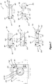
- the SM wire 510 is a wire made from a shape memory material, such as a shape memory alloy or a shape memory polymer. As assembled, the SM wire 510 is positioned in portion 500 such that the SM wire 510 is wound partially about a post of a first member 512 of the locking mechanism 504 and held in place at an opposing end by the capture connector 540. More specifically, the SM wire 510 is terminated at each end by respective termination components 604, such as barrel crimps, that are in electrical contact with the contact elements 610. Both the termination components 604 and the contact elements 610 are held in contact with each other, and retained in place, by the fixedly positioned capture connector 540 based on the tension or actuator force 125 in the SM wire 510.
- a shape memory material such as a shape memory alloy or a shape memory polymer.
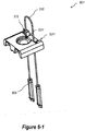
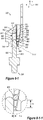
- the ends of the SM wire 510 may be terminated with termination components 604 and the SM wire 510 may be bent for insertion through the through hole 575 of the capture connector 540 (see position 601 in Fig. 6-1 ). More specifically, the SM wire 510 is threaded through the through hole 575 of the capture connector 540 from the bottom surface 541 toward the top surface 561. Then, referring to position 603 in Fig. 6-2 and position 605 in Fig. 6-3 , the SM wire 510 can be further moved through the through hole 575 and rotated down such that the SM wire 510 lies in channels 531 of the capture connector 540.
- the locking mechanism 504 may be actuated by the SM wire 510 (e.g., a nitinol wire) controlled by the processor 112 (and the memory 114) executing the electrical control function 116.
- the SM wire 510 may be controlled by the actuator 502 to contract, which can cause the first member 512 (e.g., a rocker arm) to forcibly pivot the second member 514 (e.g., a lever arm).
- the carrier 550 can contact locking protrusion 330 positioned within the aperture 341 of the locking receptacle 340 of portion 500 (e.g., first portion 302 or second portion 304) of the computing device 300, as described in Figs. 2 and 3 .
- contact from the first member 512 can cause the second member 514 to pivot on a post 516 and rotate carrier 550 relative to locking receptacle 340 (e.g., away from locking protrusion 330 that may be positioned in the aperture 341 of the locking receptacle 340).
- the post 516 for example, can be part of or can be fixed to the chassis 501 of the portion 500.
- the shape of SM wire 510 may be changed through the application of an electrical signal.
- the processor 112 and/or memory 114 executing electrical control function 116 can supply an electrical signal via one or more electrical circuits the electrical circuitry 107 to the SM wire 510 to cause the SM wire 510 to change shapes.
- the electrical signal applied to the SM wire 510 creates heat due to the internal resistance in the SM wire 510. The generated heat increases a temperature of the SM wire 510 to cause the SM wire 510 to contract, thus actuating the locking mechanism 504, until the locking mechanism 504 contacts the hardstop switch 506.
- the control components 105 and/or the actuator 502 can actuate the locking mechanism 504 to cause first member 512 to be pulled away from the second member 514, which may cause second member 514 to pivot on post 516 such to lower the carrier 550 of the locking mechanism 504 further into the aperture 341 of the locking receptacle 340.
- Moving to the locked state involves movement of the locking mechanism 504 from a second position to a first position, e.g., corresponding to movement of the surface 515 of the second member 514 from the second position 519 to the first position 517.
- the locking mechanism 504, and more specifically the carrier 550 can contact locking protrusion 330 when the locking protrusion 330 enters the aperture 341 of the locking receptacle 340, as described above.
- the gap (e.g., the distance in the y-direction between the first portion 302 and the second portion 304) between the first portion 302 and the second portion 304 in the docked configuration can be less than 0.1 mm. Having a gap less than 0.1 mm may be desirable for aesthetic and/or functional reasons. For example, for the electrical connection on the electrical protrusions 308 and the electrical connection on the electrical receptacles 309 to remain in contact, the gap should be small. In at least one implementation, a gap of 0.1 mm may be achieved while providing free play about ⁇ x of less than 1.5 degrees. The gap may be dependent on the type of locking system 320 used and/or the tolerances (e.g., the differences in the actual dimensions from the desired dimensions of the design) designed into the locking components of the locking system 320.
- a single locking system 320 can be capable of resisting a tensile force of 57 millinewtons or less applied to the locking system 320 in the y-direction without moving (e.g., less than one micron of movement) in the y-direction. In at least one implementation, a single locking system 320 can be capable of resisting a tensile force of 4 Newtons or less applied to the locking system 320 in the y-direction without substantial movement (e.g., less than 75 microns of movement) in the y-direction.
- Free play (i.e., backlash) in the y-direction of the locking protrusion 330 is movement in the y-direction when a tensile force is applied in the y-direction.
- a tensile force is applied in the y-direction.
- the top of the first portion 302 and/or the bottom of the second portion 304 are pulled with a small force (e.g., 1 Newton)
- the free play of the locking protrusion 330 in the y-direction is the distance between the first portion 302 and the second portion 304.
- Free play in the y-direction differs from the gap described above in that free play in the y-direction is the static distance between the first portion 302 and the second portion 304 when locked.
- a single locking protrusion 330 can be capable of limiting travel to less than 75 microns of movement in the y-direction when a tensile force of 4 Newtons or less applied to the locking system 320 in the y-direction.
- the insertion force applied may be small (e.g., less than 15 Newtons). In at least one implementation, the insertion force may be very small (e.g., less than 6 Newtons). In at least one implementation, the insertion force may be minimal (e.g., less than 2 Newtons). In at least one implementation, the insertion force may be substantially zero (e.g., less than 1 Newton).
- At least one implementation may only be capable of one of: having a gap between the first portion 302 and the second portion 304 of less than 0.5 mm, is capable of resisting a tensile force of 100 Newtons without separating the locking protrusion 330 from the locking receptacle 340, is capable of resisting a tensile force of 2 Newtons without moving more than 75 microns, resisting a tensile force of 28 Newtons without moving more than 0.5 mm, has free play about ⁇ x of less than 1.5 degrees about the ⁇ x-axis when a 200 N-mm torque is applied in the ⁇ x-direction, having free play in the y-direction of less than 500 microns when a 1 Newton tensile force is applied in the y-direction, having a required insertion force of less than 15 Newtons in the y-direction.
- At least one implementation may meet only one of the disclosed ranges and/or values described herein for a secure connection while failing to meet the other disclosed ranges and/or values described herein (with or without specific insertion force values and/or specific numbers of locking components). At least one implementation disclosed herein may meet two or more of the disclosed ranges and/or values described herein for a secure connection while failing to meet the other disclosed ranges and/or values described herein (with or without meeting specific insertion force values and/or specific numbers of locking components). Thus, every permutation of these values are considered a part of this disclosure.
- the locking protrusions 330 may include a planar upper surface and a planar lower surface.
- the locking protrusions 330 may have rounded (e.g., chamfered) edges, for example.
- the apertures 341 of the locking receptacles 340 on the first portion 302 are shown as being rounded on their front (e.g., in the z-direction) edges. In other implementations, the apertures 341 of the locking receptacles may be rounded on their bottom (e.g., in the negative z-direction) edges. In further implementations, the aperture 341 locking receptacle 340 may have an elongate rectangular shape. However, in implementations where the locking receptacle 340 has an elongate rectangular shape, the locking protrusion 330 may be more likely to become bound within the locking receptacle 340.
- any twist about the y- or x-axis may bind the locking protrusion 330 in the locking receptacle 340.
- the bottom would need to be pulled without significant rotation.
- some rotation may be possible without binding the locking protrusion 330 within the locking receptacle 340.
- the locking mechanism 504 may include carrier 550, which may include a front surface 852, a back surface 353, a top surface 854, a bottom surface 355, and a tapered surface 856.
- the carrier 550 may include a rotating lock aperture 859 that is configured to engage the rotating lock 860.
- the locking protrusion 330 may include a front surface 832, a back surface 833, and a top surface 834.
- the locking protrusion portion 847 of the locking receptacle 340 may be sized and/or configured to receive the locking protrusion 330.
- the carrier portion 848 of the locking receptacle 340 may be sized and/or configured to receive the carrier 550.
- the front surface 842 of the locking receptacle 340 may be sized and oriented to abut the front surface 832 of the locking protrusion 330.
- the back surface 843 of the locking receptacle 340 may be sized and oriented to abut the back surface 353 and/or bottom surface 355 of the carrier 550.
- the top surface 844 of the locking receptacle 340 may be configured to abut the top surface 834 of the locking protrusion 330 in a locked configuration.
- the tapered surface 846 of the locking receptacle 340 is angled relative to the back surface 843 of the locking receptacle 340.
- the angle may be determined by where ⁇ is the coefficient of friction of the material of the tapered surface 846 of the locking receptacle 340.
- the coefficient of friction, ⁇ , of steel is 0.1, thus the angle of the tapered surface 846 may be less than 11.4 degrees.
- the illustrated angle is ten degrees.
- the rotating lock 860 may rotate about an axis. Examples of rotating locks include a sphere, a spheroid, a cylinder, a gimbal, a cam, other rotating locks, or combinations thereof.
- the rotating lock 860 may include a front surface 862, a back surface 863, a top surface 864, and a bottom surface 865. Although described in terms of front and back surfaces 862, 863, as the rotating lock 860 rotates the front surface 862 may no longer be the "front". In other words, as the front surface 862 rotates one-hundred and eighty degrees, the front surface 862 is now in the same rotational position as the back surface 863 before rotation began.
- the front surface 862 is the portion of the outer surface of the rotating lock 860 that is closest to the back surface 833 of the locking protrusion 330
- the back surface 863 is the portion of the outer surface of the rotating lock 860 that is closest to the back surface 843 of the locking receptacle 340
- the top surface 864 is the portion of the outer surface of the rotating lock 860 that is closest to the top (e.g., in the y-direction) of the locking system 320
- the bottom surface 865 is the portion of the outer surface of the rotating lock 860 that is closest to the bottom (e.g., in the negative y-direction) of the locking system 320.
- the carrier 550 may abut a stop surface.
- the locking receptacle 340 may include a stop surface that limits movement of the carrier 550 toward the bottom of the locking system 320.
- a portion of the carrier 550 may abut a top facing (e.g., in the y-direction) surface of the locking receptacle 340.
- the carrier 550 may be in its bottom-most position.
- the rotating lock 860 may be in its top-most (e.g., in the y-direction) and front-most (e.g., in the z-direction) position, as well.
- the front surface 862 of the rotating lock 860 may extend at least partially into the locking protrusion portion 847 of the locking receptacle 340 in the undocked configuration. As can be seen in Fig. 8-1 , the front surface 862 of the rotating lock 860 extends forward (e.g., in the z-direction) beyond a plane (not shown) of the back surface 833 of the locking protrusion 330. Thus, as the locking protrusion 330 is inserted into the locking receptacle 340, the top surface 834 of the locking protrusion 330 may contact the rotating lock 860 (e.g., the front surface 862 and/or the bottom surface 865 of the rotating lock 860).
- the tapered surface 846 of the locking receptacle 340 may abut the bottom surface 865 of the rotating lock 860.
- the tapered surface 846 may be substantially planar (e.g., flat), such that the rotating lock 860 may rotate (e.g., roll) between the bottom surface 845 and the back surface 843 of the locking receptacle 340.
- the rotating lock 860 may act as a tolerance capacitor.
- the rotating lock 860 may allow a relaxation of tolerance requirements for other components of the locking mechanism.
- the rotating lock 860 as shown in Fig. 8-1-1 , may have a tolerance capacity in the z-direction and a tolerance capacity in the y-direction.
- the tolerances of the locking protrusion 330, the locking receptacle 340, and the rotating lock 860 in the z-direction may determine the locked position (e.g., the position where front surface 862 of the rotating lock 860 first abuts the back surface 833 of the locking protrusion 330) of the rotating lock 860 in the y-direction.
- the locked position of the rotating lock 860 may be independent of its position in the y-direction and/or of the y-tolerances and/or z-tolerances to the extent that the rotating lock 860 is able to move in the positive and negative y-direction.
- the rotating lock 860 may move plus or minus 0.5 mm, which soaks up about plus or minus 0.16 mm of tolerances from the locking protrusion 330, the locking receptacle 340, and the rotating lock 860 in the z-direction.
- the tolerances of these various dimensions may be very small in order to prevent binding of the locking components within the locking receptacle 340.
- the rotating lock 860 may allow a relaxation (e.g., an increase in) at least one of the various tolerances. This is due to the fact that the only requirement for the rotating lock 860 to lock the locking protrusion 330 in the locking receptacle 340 is for the rotating lock 860 to be properly seated (e.g., be positioned at least partially into the locking protrusion portion 847 of the locking receptacle 340) such that the front surface 862 of the rotating lock 860 abuts the back surface 833 of the locking protrusion 330.
- the tolerance capacity of the rotating lock 860 in the z-direction may be plus or minus 300 microns.
- one or more of the tolerances may be increased by a portion of the tolerance capacity of the rotating lock 860 in the z-direction.
- all of the tolerances in the z-direction of the locking protrusion 330, the locking receptacle 340, and the rotating lock 860 may be converted into uncertainty of the roller position.
- the rotating lock 860 may be at its extreme position.
- the tolerances in the thickness direction e.g., the z-direction
- the rotating lock 860 may soak up the tolerances in the thickness direction and convert them into position uncertainty for the rotating lock 860.
- the rotating lock 860 moves toward the top (e.g., in the y-direction) of the locking system 320.
- the top surface 834 of the locking protrusion 330 may abut and move the rotating lock 860 toward the top of the locking system 320.
- the rotating lock 860 moves both toward the top (e.g., in the y-direction) and toward the back (e.g., in the negative z-direction) of the locking system 320.
- the bottom surface 865 of the rotating lock 860 transitions from contact with the top surface 834 of the locking protrusion 330, the top surface 864 of the rotating lock 860 comes into contact with the back surface 833 of the locking protrusion 330.
- the forces being applied to the rotating lock 860 are illustrated in Fig. 8-2-1 .
- the biasing force e.g., a force applied by a biasing mechanism such as a spring
- the biasing force is applied to the top surface 864, which results in the force applied by the locking receptacle 340 (e.g., normal to the tapered surface 846) on the bottom surface 865 of the rotating lock 860 and the force applied by the locking protrusion 330 (e.g., normal to the back surface 833) on the front surface 862 of the rotating lock 860 (ignoring the force of gravity) as well as the force due to the friction (e.g., ⁇ ⁇ FReceptacle) of the locking receptacle 340 and the force due to friction (e.g., ⁇ ⁇ FProtrusion) of the locking protrusion 330.
- the forces applied to the rotating lock may differ. For example, instead of
- the rotating lock 860 may be housed by the rotating lock aperture 859 of the carrier 550.
- the rotating lock aperture 859 may couple movement of the rotating lock 860 with the carrier 550 in at least one direction.
- the rotating lock aperture 859 may couple movement of the rotating lock 860 in the top and bottom (e.g., in the y-direction) directions.
- the rotating lock aperture 859 may limit movement in the front and back (e.g., in the z-direction) direction of the rotating lock 860.
- the rotating lock aperture 859 may be shaped to correspond with at least a portion of the shape of the rotating lock 860.
- an inner surface of the rotating lock aperture 859 may be curved internally in a front portion and/or a back portion to correspond with an outer surface of the rotating lock 860.
- the front surface 852 of the carrier 550 may combine with the rotating lock aperture 859 to limit movement in the front and back direction of the rotating lock 860.
- the rotating lock 860 may abut a back facing surface in the carrier portion 848 to allow only a portion of the rotating lock 860 to enter the locking protrusion portion 847 of the locking receptacle 340.
- the rotating lock 860 may be shaped such that a left and/or right portion of the rotating lock 860 has a smaller dimension in the front and back direction than a middle portion (e.g., between the left and right portions) of the rotating lock 860, such that the middle portion still extends, at least partially, into the locking protrusion portion 847 of the locking receptacle 340 when another portion (e.g., the left and/or right portion) is prevented from doing so.
- top surface 834 of the locking protrusion 330 and the top surface 844 of the locking receptacle 340 are illustrated with complementary rounded, convex faces.
- the top surface 834 of the locking protrusion 330 and/or the top surface 844 of the locking protrusion may be otherwise shaped (e.g., complementary, not complementary, rounded, not rounded, convex, concave, or combinations thereof).
- a force must be applied to the carrier 550 to retract the rotating lock 860.
- the tapered surface 856 of the carrier 550 may cease to contact the tapered surface 846 of the locking receptacle 340.
- at least the portion of the carrier 550 that fits into the carrier portion 848 of the locking receptacle 340 may be rigid.
- the carrier 550 may be elastically deformable such that when the tapered surface 856 of the carrier 550 initially contacts the tapered surface 846 of the locking receptacle, the carrier 550 elastically deforms (e.g., bends) as the carrier 550 advances and returns toward its initial state as the carrier 550 is retracted.
- the tapered surface 856 of the carrier 550 may remain in contact with the tapered surface 846 of the locking receptacle 340 as the carrier 550 is retracted.
- the locking protrusion 330 may be removed.
- the first portion 302 and the second portion 304 may stay together in the unlocked configuration.
- the locking system 320 may return to the locked/docked configuration of Fig. 8-2 after a predetermined period of time.
- method 900 can be performed by actuated locking device 100 ( Fig. 1 ), a device employing actuated locking device 100, etc., and/or specifically electrical control function 116 or other function implemented by processor 112 of actuated locking device 100, a corresponding device, etc., to lock or unlock actuated locking device 100.
- the method 900 may be performed by the computing device 300 including the locking system 320.
- method 900 includes transmitting, via electrical circuitry, an electrical signal to a first surface of at least one contact element connectable to a body of a capture connector.
- processor 112 and/or memory 114) ( Fig. 1 ) executing electrical control function 116 transmits, via electrical circuitry 107, an electrical signal to a first surface of at least one contact element 160 connectable to a body of a capture connector 140 of actuated locking mechanism 100.
- electrical control function 116 includes programming code or instructions configured to control movement of the locking mechanism 104 between a locked state and an unlocked state, respectively corresponding to one of the first position 118 and the second position 120.
- Electrical circuitry 107 may include wiring and/or electrical connections, such as may be defined by a circuit board that includes at least one electrical interface configured to be in contact with a portion of the at least one contact element 160 in order communicate the electrical signal to the SM wire 103.
- the actuator 102 may include the capture connector 140 and the at least one contact element 160, wherein the contact element 160 is connectable to or positionable against the body of the capture connector 140.
- each contact element 160 has a first contact surface and a second contact surface.
- the at least one electrical interface of the electrical circuitry 107 e.g., a contact surface on a circuit board
- the first contact surface may extend in a first direction (e.g., perpendicular direction 131 or oblique direction 133) and the second contact surface may extend in a second direction that is different from the first direction, such as but not limited to the second direction 135.
- the capture connector 140 may include a fastener (e.g., a screw, a rivet, glue, solder, etc.) that is positionable with respect to the circuit board to connect the second contact surface of the at least one contact element with the at least one electrical interface of the circuit board.
- the fastener is configured to removably fix the capture connector 140 to the circuit board so that electrical contact between the second contact surface and the electrical interface is maintained.
- the transmitting of the electrical signal can be in response to the electrical control function 116 detecting an event for determining to actuate the locking mechanism 104 to move to one of the first position 118 or the second position 120.
- detecting the event may correspond to detecting activation of a switch or other mechanical or electromechanical feature of an actuated locking device 100, device, etc., and/or the like.
- the method 900 includes transitioning a shape memory wire to a first actuation state in response to the electrical signal being received at an actuator in electrical communication with the at least one contact element.
- SM wire 103 ( Fig. 1 ) moves to a first actuation state in response to the electrical signal being received at the actuator 102, which is in electrical communication with the at least one contact element 140 via the termination component 150.
- the SM wire 103 may extend in direction 135, and may be positioned adjacent to and/or through capture connector 140.
- the SM wire 103 has at least one of a first actuation state and a second actuation state.
- the SM wire 103 In the first actuation state the SM wire 103 has a contracted shape corresponding to moving from a first material phase to a second material phase, and in the second actuation state the SM wire 103 has an expanded shape corresponding to moving from the second material phase to the first material phase.
- the termination surface of termination component 150 is positioned for electrical contact with the first contact surface of a respective contact element 160, e.g., at electrical interface 155.
- the termination component 150 which may be a barrel crimp, is fixedly coupled to the SM wire 103.
- the termination surface of the termination component 150 such as a contact surface at an end of the longitudinal body of the barrel crimp, is configured to mate with the first contact surface of content element 160.
- the termination surface of the termination component 150 may receive the electrical signal communicated to the second contact surface of contact element 160 from the first contact surface of contact element 160 via the electrical interface 155.
- the electrical signal is received by the SM wire 103 via the termination component 150, thereby causing the SM wire 130 to heat up due to internal resistance and thereby transitioning the SM wire 103 to the first actuation state.
- method 900 includes generating an actuator force in the third direction in response to moving from the first material phase to the second material phase.
- the SM wire 103 may contract to generate the actuator force 125 in the third direction (e.g., direction 135) upon actuation by the control components 105.
- the method 900 includes transferring at least part of the actuator force in the third direction to the first contact surface of the at least one contact element.
- the termination surface of the at least one termination component 150 ( Fig. 1 ) transfers at least a part of the actuator force 125 to the first contact surface 611 of the at least one contact element 610.
- the actuator force 125 in the third direction (e.g., direction 135) is normal to or oblique to the first plane.
- the capture connector 140 maintains a fixed position, the electrical contact at electrical interface 155 between the termination surface of the termination component 150 and the first contact surface of the at least one contact element 160 is enhanced due to the actuator force 125 in the third direction.
- a solid electrical connection is maintained throughout the duration of the actuation of actuated locking device 100.
- the method 900 includes actuating a locking mechanism to move between a first position and a second position.
- actuator 102 e.g., in conjunction with processor 112, memory 114, electrical control function 116, etc.
- a locking mechanism portion e.g., locking mechanism 104
- the SM wire 103 of the actuator 102 can be actuated between different phases to control locking and unlocking of the locking mechanism 104.
- the locking mechanism 104 can provide a locking and/or unlocking action to lock a first portion of a device to a second portion of the device, unlock the first portion of the device from the second portion of the device, lock/unlock the device to/from another device, such as a similar device, a dock, one or more input devices, etc., and/or the like.
- one of the first position 118 or the second position 120 of the locking mechanism 104 may correspond to a locked state and the other one of the first position or the second position of the locking mechanism 104 may correspond to an unlocked state, or vice versa.
- the method 900 may include detecting completion of an electrical circuit at a hardstop switch caused by the locking mechanism contacting the surface of the hardstop switch at one of the first position or the second position 120.
- hardstop 106 Fig. 1
- the hardstop 106 and switch functionality e.g., in conjunction with processor 112, memory 114, and/or electrical control function 116, may detect completion of the electrical circuit at the hardstop switch (e.g., hardstop 106) caused by the locking mechanism (e.g., locking mechanism 104) contacting the hardstop switch at one of the first position 118 or the second position 120.
- the locking mechanism 104 may contact a conductive surface of the hardstop 106, which can complete the electrical connection.
- locking mechanism 104 may also be composed of an electrically conductive material and may be connected to a system ground of a device (e.g. a chassis ground of the device), such to allow completion of the electrical circuit at the hardstop switch to activate the switch.
- Processor 112 and/or electrical control function 116 may detect activation of the hardstop switch 106 in this regard.
- various configurations of the hardstop 106 are possible, examples of which are described herein, as at least a portion of a body the hardstop 106 can be electrically conductive, while the hardstop 106 may not require tolerances typically associated with separate mechanical hardstops and electrical switches.
- the method 900 may include maintaining actuation of the locking mechanism at the one of the first position 118 or the second position 120 based at least in part on detecting completion of an electrical circuit.
- actuator 102 e.g., in conjunction with processor 112, memory 114, and/or electrical control function 116, can maintain actuation of the locking mechanism (e.g., locking mechanism 104) at the one of the first position 118 or the second position 120 based at least in part on detecting completion of the electrical circuit at hardstop 106.
- maintaining actuation of the locking mechanism 104 may include maintaining a phase or shape of the SM wire 103 by modulating an electrical signal applied to, and hence a temperature of, the SM wire 103 in an attempt to substantially maintain the temperature of the SM wire 103, and thus electrical contact of the locking mechanism 104 to the hardstop 106.
- electrical control function 116 and/or actuator 102 may include known electrical signal versus SM wire phase change relationships (e.g., turn the signal on and/or off for certain amounts of time to obtain or maintain a certain amount of phase change) that enable electrical control function 116 via processor 112 to modulate the electrical signal supplied to the SM wire 103 to cause and/or maintain contact of locking mechanism 104 with a conductive surface of hardstop 106.
- actuator 102 can increase the temperature of the SM wire 103 when the electrical contact between the locking mechanism 104 and the hardstop 106 begins to degrade or otherwise ceases and electrical control function 116 wants to maintain the electrical contact.
- actuation of the locking mechanism 104 can be maintained in this regard. For example, this can cause the locking mechanism 104 to remain in the locked or unlocked state defined by the first position 118 or the second position 120 in which actuation of the locking mechanism 104 is maintained.
- An example actuator mechanism for joining two portions of a computing device, includes a capture connector having a body, at least one contact element connected to the body, wherein each contact element comprises a first contact surface extending in a first direction and a second contact surface extending in a second direction different from the first direction, a shape memory wire extending in a third direction adjacent to the capture connector, wherein the shape memory wire has a first actuation state and a second actuation state, wherein in the first actuation state the shape memory wire has a contracted shape corresponding to moving from a first material phase to a second material phase, and wherein in the second actuation state the shape memory wire has an expanded shape corresponding to moving from the second material phase to the first material phase, at least one termination component fixedly coupled to the shape memory wire, wherein the termination component comprises a termination surface shaped for electrical contact with the first contact surface of a respective contact element, and wherein in the first actuation state or the second actuation state, the shape memory wire is configured to generate an actuator force such that the termination
- An example actuator mechanism of any preceding actuator mechanism includes the first contact surface of the at least one contact element and the termination surface of the termination component substantially lie in a first plane extending in the first direction, and wherein the actuator force in the third direction is oblique to the first plane.
- Another example actuator mechanism of any preceding actuator mechanism includes the first contact surface of the at least one contact element and the termination surface of the termination component substantially lie in a first plane extending in the first direction, and wherein the actuator force in the third direction is substantially normal to the first plane.
- Another example actuator mechanism of any preceding actuator mechanism includes a circuit board having at least one electrical interface shaped to contact the second contact surface of the at least one contact element, wherein the first contact surface of the at least one contact element and the termination surface of the termination component substantially lie in a first plane extending in the first direction, and wherein the first plane is divergent from a plane of the second contact surface and the electrical interface of the circuit board.
- Another example actuator mechanism of any preceding actuator mechanism includes a fastener positionable with respect to the circuit board to connect the second contact surface of the at least one contact element with the at least one electrical interface of the circuit board.
- Another example actuator mechanism of any preceding actuator mechanism includes the capture connector further comprises a first mating component and the circuit board or a chassis to which the circuit board is mounted comprises a second mating component having a shape corresponding to the first mating component, wherein the first mating component and the second mating component fit together to substantially resist at least one of a relative rotation and a relative translation between the capture connector and the circuit board.
- Another example actuator mechanism of any preceding actuator mechanism includes a locking mechanism connectable to the shape memory wire, wherein the locking mechanism has a locked state and an unlocked state each corresponding to a respective one of the first actuation state and the second actuation state of the shape memory wire.
- Another example actuator mechanism of any preceding actuator mechanism includes the first contact surface of the at least one contact element includes an inner contact wall defining an opening sized to receive the shape memory wire.
- Another example actuator mechanism of any preceding actuator mechanism includes the capture connector includes an inner connector wall defining a channel sized to receive the shape memory wire.
- Another example actuator mechanism of any preceding actuator mechanism includes at least one non-conductive spacers located below the at least one termination component, wherein the at least one non-conductive spacer has a thickness to bias the termination component to maximize a contact surface area between the termination surface of the termination component and the first contact surface of the at least one contact element.
- An example computing device includes a first portion having a first set of computing components, a second portion having a second set of computing components, wherein the second portion is removably attachable to the first portion, a locking mechanism having a locked state and an unlocked state, wherein the locked state corresponds to a fixed attachment of the first portion and the second portion, and wherein the unlocked state corresponds to a release of the fixed attachment of the first portion and the second portion, an actuator mechanism having a first actuation state and a second actuation state each corresponding to one of the locked state and the unlocked state, wherein the actuator mechanism includes a capture connector having a body, at least one contact element connectable to the body, wherein each contact element comprises a first contact surface extending in a first direction and a second contact surface extending in a second direction different from the first direction, a shape memory wire extending in a third direction adjacent to the capture connector, wherein the shape memory wire has a contracted shape corresponding to moving from a first material phase to a second material phase in the
- Another example computing device of any preceding computing device includes the first contact surface of the at least one contact element and the termination surface of the termination component substantially lie in a first plane extending in the first direction, and wherein the actuator force in the third direction is oblique to the first plane.
- Another example computing device of any preceding computing device includes the first contact surface of the at least one contact element and the termination surface of the termination component substantially lie in a first plane extending in the first direction, and wherein the actuator force in the third direction is substantially normal to the first plane.
- Another example computing device of any preceding computing device includes a circuit board having at least one electrical interface shaped to contact the second contact surface of the at least one contact element, wherein the first contact surface of the at least one contact element and the termination surface of the termination component substantially lie in a first plane extending in the first direction, and wherein the first plane is divergent from a plane of the second contact surface and the electrical interface of the circuit board.
- Another example computing device of any preceding computing device includes a fastener positionable with respect to the circuit board to connect the second contact surface of the at least one contact element with the at least one electrical interface of the circuit board.
- Another example computing device of any preceding computing device includes the capture connector further comprises a first mating component and the circuit board or a chassis to which the circuit board is mounted comprises a second mating component having a shape corresponding to the first mating component, wherein the first mating component and the second mating component fit together to substantially resist at least one of a relative rotation and a relative translation between the capture connector and the circuit board.
- Another example computing device of any preceding computing device includes the first contact surface of the at least one contact element includes an inner contact wall defining an opening sized to receive the shape memory wire, and wherein the capture connector includes an inner connector wall defining a channel sized to receive the shape memory wire.
- Another example computing device of any preceding computing device includes at least one non-conductive spacers located below the at least one termination component, wherein the at least one non-conductive spacer has a thickness to bias the termination component to maximize a contact surface area between the termination surface of the termination component and the first contact surface of the at least one contact element.
- An example method for operating an actuator for joining two portions of a computing device includes transmitting, via at least one electrical interface of a circuit, an electrical signal to a first contact surface of at least one contact element connected to a body of a capture connector, wherein the first contact surface extends in a first direction, wherein the least one contact element includes a second contact surface extending in a second direction that is in electrical contact with a termination surface of at least one termination component fixedly coupled to a shape memory wire extending in a third direction, transitioning the shape memory wire to a first actuation state based on the electrical signal transmitted to the first contact surface, wherein in the first actuation state the shape memory wire has a contracted shape corresponding to moving from a first material phase to a second material phase, generating, by the shape memory wire, an actuator force in the third direction in response to moving from the first material phase to the second material phase, and transferring, by the termination surface of the at least one termination component, at least part of the actuator force in the third direction to the first contact surface of the at least one
- Another example method of any preceding method includes actuating a locking mechanism to move between a first position and a second position in response to the shape memory wire generating the actuator force, detecting completion of an electrical circuit at a hardstop switch caused by the locking mechanism contacting the hardstop switch at one of the first position or the second position, and maintaining actuation of the locking mechanism at the one of the first position or the second position based at least in part on detecting completion of the electrical circuit.
- an actuated locking device has been described above with reference to various systems and methods.
- One or more portions of these systems and methods may have been described or illustrated in the accompanying drawings by various blocks, modules, components, circuits, steps, processes, algorithms, etc. (collectively referred to as "elements").
- One or more of these elements may be implemented using electronic hardware, computer software, or any combination thereof. Whether such elements are implemented as hardware or software depends upon the particular application and design constraints imposed on the overall system.
- processors include microprocessors, microcontrollers, digital signal processors (DSPs), field programmable gate arrays (FPGAs), programmable logic devices (PLDs), state machines, gated logic, discrete hardware circuits, and other suitable hardware configured to perform the various functionality described throughout this disclosure.
- DSPs digital signal processors
- FPGAs field programmable gate arrays
- PLDs programmable logic devices
- state machines gated logic, discrete hardware circuits, and other suitable hardware configured to perform the various functionality described throughout this disclosure.
- One or more processors in the processing system may execute software.
- Software shall be construed broadly to mean instructions, instruction sets, code, code segments, program code, programs, subprograms, software modules, applications, software applications, software packages, routines, subroutines, objects, executables, threads of execution, procedures, functions, etc., whether referred to as software, firmware, middleware, microcode, hardware description language, or otherwise.
- one or more of the functions described may be implemented in hardware, software, firmware, or any combination thereof. If implemented in software, the functions may be stored on or encoded as one or more instructions or code on a computer-readable medium.
- Computer-readable media includes computer storage media. Storage media may be any available media that can be accessed by a computer. By way of example, and not limitation, such computer-readable media can comprise RAM, ROM, EEPROM, CD-ROM or other optical disk storage, magnetic disk storage or other magnetic storage devices, or any other medium that can be used to carry or store desired program code in the form of instructions or data structures and that can be accessed by a computer.
- Disk and disc includes compact disc (CD), laser disc, optical disc, digital versatile disc (DVD), and floppy disk where disks usually reproduce data magnetically, while discs reproduce data optically with lasers. Combinations of the above should also be included within the scope of computer-readable media.
Landscapes
- Engineering & Computer Science (AREA)
- Theoretical Computer Science (AREA)
- Computer Hardware Design (AREA)
- General Engineering & Computer Science (AREA)
- Physics & Mathematics (AREA)
- Combustion & Propulsion (AREA)
- Chemical & Material Sciences (AREA)
- General Physics & Mathematics (AREA)
- Human Computer Interaction (AREA)
- Mechanical Engineering (AREA)
- Mathematical Physics (AREA)
- Signal Processing (AREA)
- Details Of Connecting Devices For Male And Female Coupling (AREA)
Claims (15)
- Aktuator-Mechanismus (400) zum Verbinden zweier Abschnitte einer Rechenvorrichtung, umfassend:einen Fangverbinder (540) mit einem Körper (600);mindestens ein Kontaktelement (610), das mit dem Körper (600) verbunden ist, wobei jedes Kontaktelement (610) eine erste Kontaktfläche (611) umfasst, die sich in einer ersten Richtung (131) erstreckt, und eine zweite Kontaktfläche (613), die sich in einer zweiten, von der ersten Richtung verschiedenen Richtung (135) erstreckt;einen Formgedächtnisdraht (510), der sich in einer dritten Richtung angrenzend an den Fangverbinder (540) erstreckt, wobei der Formgedächtnisdraht (510) einen ersten Betätigungszustand und einen zweiten Betätigungszustand aufweist, wobei in dem ersten Betätigungszustand der Formgedächtnisdraht (510) eine kontrahierte Form aufweist, die einer Bewegung von einer ersten Materialphase zu einer zweiten Materialphase entspricht, und wobei in dem zweiten Betätigungszustand der Formgedächtnisdraht (510) eine expandierte Form aufweist, die einer Bewegung von der zweiten Materialphase zu der ersten Materialphase entspricht;mindestens eine Abschlusskomponente (604), die fest mit dem Formgedächtnisdraht (510) gekoppelt ist, wobei die Abschlusskomponente (604) eine Abschlussfläche (644) umfasst, die für einen elektrischen Kontakt mit der ersten Kontaktfläche (611) eines jeweiligen Kontaktelements (610) geformt ist; undwobei in dem ersten Betätigungszustand oder dem zweiten Betätigungszustand der Formgedächtnisdraht (510) konfiguriert ist, um eine Aktuatorkraft (125) zu erzeugen, so dass die Abschlussfläche (644) der mindestens einen Abschlusskomponente (604) zumindest einen Teil der Aktuatorkraft in der dritten Richtung auf die erste Kontaktfläche (611) des mindestens einen Kontaktelements (610) überträgt, wobei die dritte Richtung von der ersten Richtung abweicht.
- Aktuator-Mechanismus nach Anspruch 1, wobei die erste Kontaktfläche (611) des mindestens einen Kontaktelements (610) und die Abschlussfläche (644) der Abschlusskomponente (604) im Wesentlichen in einer ersten Ebene liegen, die sich in der ersten Richtung erstreckt, und wobei die Aktuatorkraft in der dritten Richtung (133) schräg zu der ersten Ebene verläuft.
- Aktuator-Mechanismus nach Anspruch 1, wobei die erste Kontaktfläche (611) des mindestens einen Kontaktelements (610) und die Abschlussfläche (644) der Abschlusskomponente (604) im Wesentlichen in einer ersten Ebene liegen, die sich in der ersten Richtung erstreckt, und wobei die Aktuatorkraft in der dritten Richtung im Wesentlichen normal zu der ersten Ebene verläuft.
- Aktuator-Mechanismus nach Anspruch 1, weiter umfassend:eine Leiterplatte (532), die mindestens eine elektrische Schnittstelle (602) aufweist, die so geformt ist, dass sie die zweite Kontaktfläche (613) des mindestens einen Kontaktelements (610) kontaktiert;wobei die erste Kontaktfläche (611) des mindestens einen Kontaktelements (610) und die Abschlussfläche (644) der Abschlusskomponente (604) im Wesentlichen in einer ersten Ebene liegen, die sich in der ersten Richtung erstreckt; undwobei die erste Ebene von einer Ebene der zweiten Kontaktfläche und der elektrischen Schnittstelle (602) der Leiterplatte (532) abweicht; undein Befestigungselement (606), das in Bezug auf die Leiterplatte (532) positionierbar ist, um die zweite Kontaktfläche (613) des mindestens einen Kontaktelements (610) mit der mindestens einen elektrischen Schnittstelle (602) der Leiterplatte (532) zu verbinden.
- Aktuator-Mechanismus nach Anspruch 4, wobei der Fangverbinder (540) weiter eine erste Gegenkomponente (567) umfasst und die Leiterplatte (532) oder ein Chassis, an dem die Leiterplatte (532) befestigt ist, eine zweite Gegenkomponente (537) umfasst, die eine Form hat, die der ersten Gegenkomponente (567) entspricht, wobei die erste Gegenkomponente (567) und die zweite Gegenkomponente (537) zusammenpassen, um im Wesentlichen einer relativen Rotation und/oder einer relativen Translation zwischen dem Fangverbinder (540) und der Leiterplatte (532) zu widerstehen.
- Aktuator-Mechanismus nach Anspruch 1, weiter umfassend:
einen Verriegelungsmechanismus (504), der mit dem Formgedächtnisdraht (510) verbindbar ist, wobei der Verriegelungsmechanismus (504) einen verriegelten Zustand und einen entriegelten Zustand aufweist, die jeweils einem jeweiligen von dem ersten Betätigungszustand und dem zweiten Betätigungszustand des Formgedächtnisdrahtes (510) entsprechen, wobei die erste Kontaktoberfläche (611) des mindestens einen Kontaktelements (610) eine innere Kontaktwand (573) einschließt, die eine Öffnung definiert, die so bemessen ist, dass sie den Formgedächtnisdraht (510) empfängt, und wobei der Fangverbinder (540) eine innere Verbinderwand (577) einschließt, die einen Kanal definiert, der so bemessen ist, dass er den Formgedächtnisdraht (510) empfängt. - Aktuator-Mechanismus nach Anspruch 1, weiter umfassend mindestens einen nicht leitfähigen Abstandshalter (608), der unter der mindestens einen Abschlusskomponente (604) angeordnet ist, wobei der mindestens eine nicht leitfähige Abstandshalter (608) eine Dicke aufweist, um die Abschlusskomponente (604) so vorzuspannen, dass ein Kontaktflächenbereich zwischen der Abschlussfläche (644) der Abschlusskomponente (604) und der ersten Kontaktfläche (611) des mindestens einen Kontaktelements (610) maximiert wird.
- Rechenvorrichtung, umfassend:einen ersten Abschnitt (302) mit einem ersten Satz von Rechenkomponenten;einen zweiten Abschnitt (304), mit einem zweiten Satz von Rechenkomponenten, wobei der zweite Abschnitt (304) abnehmbar an dem ersten Abschnitt (302) anbringbar ist;einen Verriegelungsmechanismus (320) mit einem verriegelten Zustand und einem entriegelten Zustand, wobei der verriegelte Zustand einem festen Anbringen des ersten Abschnitts (302) und des zweiten Abschnitts (304) entspricht, und wobei der entriegelte Zustand einem Lösen aus dem festen Anbringen des ersten Abschnitts (302) und des zweiten Abschnitts (304) entspricht;einen Aktuator-Mechanismus mit einem ersten Betätigungszustand und einem zweiten Betätigungszustand, die jeweils einem von dem verriegelten Zustand und dem entriegelten Zustand entsprechen, wobei der Aktuator-Mechanismus (400) der Aktuator-Mechanismus (400) von Anspruch 1 ist.
- Rechenvorrichtung nach Anspruch 8, wobei die erste Kontaktfläche (611) des mindestens einen Kontaktelements (610) und die Abschlussfläche (644) der Abschlusskomponente (604) im Wesentlichen in einer ersten Ebene liegen, die sich in der ersten Richtung erstreckt, und wobei die Aktuatorkraft in der dritten Richtung schräg zu der ersten Ebene verläuft.
- Rechenvorrichtung nach Anspruch 8, wobei die erste Kontaktfläche (611) des mindestens einen Kontaktelements (610) und die Abschlussfläche (644) der Abschlusskomponente (604) im Wesentlichen in einer ersten Ebene liegen, die sich in der ersten Richtung erstreckt, und wobei die Aktuatorkraft in der dritten Richtung im Wesentlichen normal zu der ersten Ebene verläuft.
- Rechenvorrichtung nach Anspruch 8, weiter umfassend:eine Leiterplatte (532), die mindestens eine elektrische Schnittstelle (602) aufweist, die so geformt ist, dass sie die zweite Kontaktfläche (613) des mindestens einen Kontaktelements (610) kontaktiert;wobei die erste Kontaktfläche (611) des mindestens einen Kontaktelements (610) und die Abschlussfläche (644) der Abschlusskomponente (604) im Wesentlichen in einer ersten Ebene liegen, die sich in der ersten Richtung erstreckt; undwobei die erste Ebene von einer Ebene der zweiten Kontaktfläche (613) und der elektrischen Schnittstelle (602) der Leiterplatte (532) abweicht; undein Befestigungselement (606), das in Bezug auf die Leiterplatte positionierbar ist, um die zweite Kontaktfläche (613) des mindestens einen Kontaktelements (610) mit der mindestens einen elektrischen Schnittstelle (602) der Leiterplatte (532) zu verbinden.
- Rechenvorrichtung nach Anspruch 11, wobei der Fangverbinder (540) weiter eine erste Gegenkomponente (567) umfasst und die Leiterplatte (532) oder ein Chassis, an dem die Leiterplatte (532) befestigt ist, eine zweite Gegenkomponente (537) umfasst, die eine Form hat, die der ersten Gegenkomponente (567) entspricht, wobei die erste Gegenkomponente (567) und die zweite Gegenkomponente (537) zusammenpassen, um im Wesentlichen einer relativen Rotation und/oder einer relativen Translation zwischen dem Fangverbinder (540) und der Leiterplatte (532) zu widerstehen.
- Rechenvorrichtung nach Anspruch 8, wobei die erste Kontaktfläche (611) des mindestens einen Kontaktelements (610) eine innere Kontaktwand (573) einschließt, die eine Öffnung definiert, die so bemessen ist, dass sie den Formgedächtnisdraht (510) empfängt, und wobei der Fangverbinder (5470) eine innere Verbinderwand (577) einschließt, die einen Kanal definiert, der so bemessen ist, dass er den Formgedächtnisdraht (510) empfängt.
- Rechenvorrichtung nach Anspruch 8, weiter umfassend mindestens einen nicht leitfähigen Abstandshalter (608), der unter der mindestens einen Abschlusskomponente (604) angeordnet ist, wobei der mindestens eine nicht leitfähige Abstandshalter (608) eine Dicke aufweist, um die Abschlusskomponente (604) so vorzuspannen, dass ein Kontaktflächenbereich zwischen der Abschlussfläche (644) der Abschlusskomponente (604) und der ersten Kontaktfläche (611) des mindestens einen Kontaktelements (610) maximiert wird.
- Verfahren (900) zum Betreiben eines Aktuator-Mechanismus (400) nach einem der Ansprüche 1 bis 7 zum Verbinden zweier Abschnitte einer Rechenvorrichtung, umfassend:Übertragen (902) eines elektrischen Signals über mindestens eine elektrische Schnittstelle einer Schaltung an eine erste Kontaktfläche (611) von mindestens einem Kontaktelement (610), das mit einem Körper eines Fangverbinders (540) verbunden ist, wobei sich die erste Kontaktfläche (611) in einer ersten Richtung erstreckt, wobei das mindestens eine Kontaktelement (610) eine zweite Kontaktfläche (613) einschließt, die sich in einer zweiten Richtung erstreckt, die in elektrischem Kontakt mit einer Abschlussfläche (644) von mindestens einer Abschlusskomponente (604) steht, die fest mit einem Formgedächtnisdraht (510) verbunden ist, der sich in einer dritten Richtung erstreckt;Überführen (904) des Formgedächtnisdrahtes (510) in einen ersten Betätigungszustand basierend auf der ersten Kontaktfläche (611) gesendeten elektrischen Signals, wobei der Formgedächtnisdraht (510) in dem ersten Betätigungszustand eine kontrahierte Form aufweist, die der Bewegung von einer ersten Materialphase in eine zweite Materialphase entspricht;Erzeugen (906) einer Aktuatorkraft in der dritten Richtung durch den Formgedächtnisdraht (510) als Reaktion auf die Bewegung von der ersten Materialphase in die zweite Materialphase; undÜbertragen (908,) durch die Abschlussfläche (644) der mindestens einen Abschlusskomponente (604), zumindest eines Teils der Aktuatorkraft in der dritten Richtung auf die erste Kontaktfläche (611) des mindestens einen Kontaktelements (610), wobei die dritte Richtung von der ersten abweicht.
Applications Claiming Priority (2)
| Application Number | Priority Date | Filing Date | Title |
|---|---|---|---|
| US15/240,866 US9785196B1 (en) | 2016-08-18 | 2016-08-18 | Capture connector for actuated locking devices |
| PCT/US2017/046456 WO2018034967A1 (en) | 2016-08-18 | 2017-08-11 | Capture connector for actuated locking devices |
Publications (2)
| Publication Number | Publication Date |
|---|---|
| EP3501162A1 EP3501162A1 (de) | 2019-06-26 |
| EP3501162B1 true EP3501162B1 (de) | 2021-08-11 |
Family
ID=59762039
Family Applications (1)
| Application Number | Title | Priority Date | Filing Date |
|---|---|---|---|
| EP17761356.9A Active EP3501162B1 (de) | 2016-08-18 | 2017-08-11 | Fangverbinder für betätigte verriegelungsvorrichtungen |
Country Status (4)
| Country | Link |
|---|---|
| US (2) | US9785196B1 (de) |
| EP (1) | EP3501162B1 (de) |
| CN (1) | CN109644213B (de) |
| WO (1) | WO2018034967A1 (de) |
Families Citing this family (11)
| Publication number | Priority date | Publication date | Assignee | Title |
|---|---|---|---|---|
| US9740245B2 (en) | 2015-10-05 | 2017-08-22 | Microsoft Technology Licensing, Llc | Locking mechanism |
| US9910463B1 (en) * | 2016-08-12 | 2018-03-06 | Microsoft Technology Licensing, Llc | Combination hardstop and switch for actuated locking devices |
| US11188128B2 (en) * | 2016-10-17 | 2021-11-30 | Lenovo (Singapore) Pte. Ltd. | Convertible electronic apparatus |
| JP2018200522A (ja) * | 2017-05-26 | 2018-12-20 | レノボ・シンガポール・プライベート・リミテッド | 電子機器 |
| US10303214B2 (en) | 2017-10-17 | 2019-05-28 | Microsoft Technology Licensing, Llc | Docking mechanisms and methods of restraining two portions of a computing device |
| US10893724B2 (en) | 2017-11-01 | 2021-01-19 | Microsoft Technology Licensing, Llc | Locking mechanisms in electronic devices |
| EP4046865A1 (de) * | 2021-02-17 | 2022-08-24 | Windsor Machine and Stamping (2009) Ltd. | Kopfstützenverriegelung mit formgedächtnislegierungsauslösevorrichtung |
| US11487332B2 (en) * | 2021-03-23 | 2022-11-01 | Dell Products L.P. | Systems and methods for determining hinge angle position in an information handling system |
| CN113086254B (zh) * | 2021-04-14 | 2022-09-02 | 电子科技大学 | 一种用于航空环境的简易解锁装置 |
| JP7251578B2 (ja) * | 2021-08-18 | 2023-04-04 | カシオ計算機株式会社 | 電子機器 |
| CN115459010B (zh) * | 2022-09-30 | 2025-04-08 | Oppo广东移动通信有限公司 | 锁定机构、壳体及电子设备 |
Family Cites Families (32)
| Publication number | Priority date | Publication date | Assignee | Title |
|---|---|---|---|---|
| US4969835A (en) | 1987-10-22 | 1990-11-13 | The Furukawa Electric Company, Ltd. | Reinforced connection for a electronic circuit members and method for constructing therefor |
| US4841283A (en) * | 1987-12-21 | 1989-06-20 | Southern Steel Company | Security hinge utilizing concealed radiative sensing to detect hinge position |
| US5564936A (en) | 1994-12-07 | 1996-10-15 | Berg Technology, Inc. | Card security mechanism for a memory card connector and method of use |
| WO1998021640A1 (en) | 1996-11-15 | 1998-05-22 | Agate Technologies, Inc. | Hot swapable drive/dock with software drivers for ide interface |
| US5831820A (en) | 1996-12-30 | 1998-11-03 | Huang; James | Peripheral docking module using a shape memory alloy actuator wire |
| US6133816A (en) | 1998-06-12 | 2000-10-17 | Robertshaw Controls Corp. | Switch and relay using shape memory alloy |
| US5990777A (en) | 1998-08-05 | 1999-11-23 | The Whitaker Corporation | Shape-memory wire actuated switch |
| US6917276B1 (en) | 2000-06-19 | 2005-07-12 | Simpler Networks | Bistable switch with shape memory metal |
| US20020069483A1 (en) * | 2000-12-08 | 2002-06-13 | Pertti Savolainen | Apparatus for opening hand held electronic device |
| US7042714B2 (en) * | 2001-11-08 | 2006-05-09 | Apple Computer, Inc. | Computer controlled display device |
| US7209344B2 (en) * | 2001-11-08 | 2007-04-24 | Apple Inc. | Computer controlled display device |
| JP4186664B2 (ja) | 2003-03-24 | 2008-11-26 | 松下電器産業株式会社 | スイッチ装置 |
| EP1626177A1 (de) | 2003-05-12 | 2006-02-15 | Mitsubishi Denki Kabushiki Kaisha | Antriebseinrichtung |
| CN100576329C (zh) * | 2003-08-28 | 2009-12-30 | 松下电器产业株式会社 | 动作装置、位置切换装置及光磁记录再生装置 |
| US7133280B2 (en) * | 2004-03-22 | 2006-11-07 | Gateway Inc. | Multiaxial hinge assembly with rotational direction indicator |
| TWI312926B (en) * | 2005-12-22 | 2009-08-01 | Asustek Comp Inc | Electronic device with a power control function |
| US8117938B2 (en) | 2006-07-05 | 2012-02-21 | Ghsp, Inc. | Shifter with shape memory alloy and safety |
| JP5429932B2 (ja) | 2009-08-25 | 2014-02-26 | オリンパス株式会社 | 形状記憶合金アクチュエータ |
| KR101301631B1 (ko) * | 2009-12-11 | 2013-08-29 | 후지쯔 가부시끼가이샤 | 로크 장치, 전자 기기 및 로크 방법 |
| US8827331B2 (en) * | 2011-06-06 | 2014-09-09 | International Business Machines Corporation | Shape memory alloy locking mechanism |
| PL221673B1 (pl) | 2011-12-20 | 2016-05-31 | Bitron Poland Spółka Z Ograniczoną Odpowiedzialnością | Elektrycznie sterowane urządzenie uruchamiające i urządzenie dozujące |
| GB2514071B (en) | 2012-02-16 | 2015-09-16 | Cambridge Mechatronics Ltd | Shape memory alloy actuation apparatus |
| CN104737088A (zh) | 2012-03-28 | 2015-06-24 | 尤塔设备Ipr有限公司 | 包括显示器和硬件功率按钮的显示设备 |
| TWI499894B (zh) * | 2012-11-06 | 2015-09-11 | Compal Electronics Inc | 電子裝置 |
| ITMI20121988A1 (it) | 2012-11-22 | 2014-05-23 | Getters Spa | Elemento attuatore con migliorata resistenza a fatica fatto di una lega a memoria di forma |
| TWI502323B (zh) * | 2013-08-23 | 2015-10-01 | Acer Inc | 擴充基座 |
| EP2866121A1 (de) * | 2013-10-28 | 2015-04-29 | Acco Brands Corporation | Tragbares elektronisches Vorrichtungsgehäuse, Blatt und Ladebrücke |
| JP5999381B2 (ja) * | 2014-06-20 | 2016-09-28 | Smk株式会社 | 駆動装置 |
| US9939848B2 (en) * | 2014-08-29 | 2018-04-10 | Dell Products L.P. | Portable information handling system detachable support and attachment device |
| US9740245B2 (en) * | 2015-10-05 | 2017-08-22 | Microsoft Technology Licensing, Llc | Locking mechanism |
| US9910463B1 (en) * | 2016-08-12 | 2018-03-06 | Microsoft Technology Licensing, Llc | Combination hardstop and switch for actuated locking devices |
| US9646179B1 (en) * | 2016-12-30 | 2017-05-09 | Foxrun Development Co., LLC | Mechanical locking device for computer ports and portable storage devices |
-
2016
- 2016-08-18 US US15/240,866 patent/US9785196B1/en not_active Expired - Fee Related
-
2017
- 2017-08-11 EP EP17761356.9A patent/EP3501162B1/de active Active
- 2017-08-11 WO PCT/US2017/046456 patent/WO2018034967A1/en not_active Ceased
- 2017-08-11 CN CN201780050840.0A patent/CN109644213B/zh active Active
- 2017-09-28 US US15/719,293 patent/US10088874B2/en active Active
Also Published As
| Publication number | Publication date |
|---|---|
| US10088874B2 (en) | 2018-10-02 |
| CN109644213A (zh) | 2019-04-16 |
| CN109644213B (zh) | 2021-01-22 |
| US9785196B1 (en) | 2017-10-10 |
| EP3501162A1 (de) | 2019-06-26 |
| WO2018034967A1 (en) | 2018-02-22 |
| US20180052495A1 (en) | 2018-02-22 |
Similar Documents
| Publication | Publication Date | Title |
|---|---|---|
| EP3501162B1 (de) | Fangverbinder für betätigte verriegelungsvorrichtungen | |
| EP3497536B1 (de) | Kombinationsanschlag und schalter für betätigte verriegelungsvorrichtung | |
| US7083459B1 (en) | Latching connector assembly | |
| CN108139777B (zh) | 锁定机构 | |
| WO2018155363A1 (ja) | 電子機器 | |
| CN101077042B (zh) | 用于改进的卡边缘连接器的系统和方法 | |
| US8817476B2 (en) | Apparatus, add-on module, and a system comprising a host apparatus and an add-on module | |
| JPWO2018155365A1 (ja) | 外部ロック装置 | |
| US20040106318A1 (en) | Self-locking mechanism for a hot pluggable printed circuit board | |
| US20060057879A1 (en) | Latch for connecting a component to a device | |
| US20070211424A1 (en) | Apparatus for mounting removably a disk drive in an electronic device | |
| EP3449335B1 (de) | Abkopplungsunterstützungsvorrichtung und verfahren zur verwendung | |
| JP4764573B2 (ja) | ケーブルコネクタ | |
| CN202443359U (zh) | 滑动式连接器机构及其相关薄型可携式电子装置 | |
| EP3902070B1 (de) | Passender steckverbinder | |
| US5989051A (en) | Connector for joining a cable to a PCMCIA card | |
| US20070035275A1 (en) | Backup battery assembly for electronic device | |
| CN108868390B (zh) | 车辆用锁定装置 | |
| WO2024168130A1 (en) | Robust, miniaturized ffc connector | |
| CN217239893U (zh) | 锁定件、插拔模组及电子设备 | |
| JP3270025B2 (ja) | ドッキングステーション | |
| JP4922206B2 (ja) | 電子装置と拡張ユニットとの接続装置 | |
| CN220726025U (zh) | 一种箱柜锁及快递柜 | |
| CN222391214U (zh) | 一种共享移动电源的防盗锁止机构 | |
| CN223638707U (zh) | 一种电连接器 |
Legal Events
| Date | Code | Title | Description |
|---|---|---|---|
| STAA | Information on the status of an ep patent application or granted ep patent |
Free format text: STATUS: UNKNOWN |
|
| STAA | Information on the status of an ep patent application or granted ep patent |
Free format text: STATUS: THE INTERNATIONAL PUBLICATION HAS BEEN MADE |
|
| PUAI | Public reference made under article 153(3) epc to a published international application that has entered the european phase |
Free format text: ORIGINAL CODE: 0009012 |
|
| STAA | Information on the status of an ep patent application or granted ep patent |
Free format text: STATUS: REQUEST FOR EXAMINATION WAS MADE |
|
| 17P | Request for examination filed |
Effective date: 20190214 |
|
| AK | Designated contracting states |
Kind code of ref document: A1 Designated state(s): AL AT BE BG CH CY CZ DE DK EE ES FI FR GB GR HR HU IE IS IT LI LT LU LV MC MK MT NL NO PL PT RO RS SE SI SK SM TR |
|
| AX | Request for extension of the european patent |
Extension state: BA ME |
|
| DAV | Request for validation of the european patent (deleted) | ||
| DAX | Request for extension of the european patent (deleted) | ||
| GRAP | Despatch of communication of intention to grant a patent |
Free format text: ORIGINAL CODE: EPIDOSNIGR1 |
|
| STAA | Information on the status of an ep patent application or granted ep patent |
Free format text: STATUS: GRANT OF PATENT IS INTENDED |
|
| GRAJ | Information related to disapproval of communication of intention to grant by the applicant or resumption of examination proceedings by the epo deleted |
Free format text: ORIGINAL CODE: EPIDOSDIGR1 |
|
| STAA | Information on the status of an ep patent application or granted ep patent |
Free format text: STATUS: REQUEST FOR EXAMINATION WAS MADE |
|
| INTG | Intention to grant announced |
Effective date: 20210215 |
|
| GRAP | Despatch of communication of intention to grant a patent |
Free format text: ORIGINAL CODE: EPIDOSNIGR1 |
|
| STAA | Information on the status of an ep patent application or granted ep patent |
Free format text: STATUS: GRANT OF PATENT IS INTENDED |
|
| INTC | Intention to grant announced (deleted) | ||
| INTG | Intention to grant announced |
Effective date: 20210406 |
|
| GRAS | Grant fee paid |
Free format text: ORIGINAL CODE: EPIDOSNIGR3 |
|
| GRAA | (expected) grant |
Free format text: ORIGINAL CODE: 0009210 |
|
| STAA | Information on the status of an ep patent application or granted ep patent |
Free format text: STATUS: THE PATENT HAS BEEN GRANTED |
|
| AK | Designated contracting states |
Kind code of ref document: B1 Designated state(s): AL AT BE BG CH CY CZ DE DK EE ES FI FR GB GR HR HU IE IS IT LI LT LU LV MC MK MT NL NO PL PT RO RS SE SI SK SM TR |
|
| REG | Reference to a national code |
Ref country code: CH Ref legal event code: EP |
|
| REG | Reference to a national code |
Ref country code: DE Ref legal event code: R096 Ref document number: 602017043877 Country of ref document: DE |
|
| REG | Reference to a national code |
Ref country code: IE Ref legal event code: FG4D Ref country code: AT Ref legal event code: REF Ref document number: 1420574 Country of ref document: AT Kind code of ref document: T Effective date: 20210915 |
|
| RAP4 | Party data changed (patent owner data changed or rights of a patent transferred) |
Owner name: MICROSOFT TECHNOLOGY LICENSING, LLC |
|
| REG | Reference to a national code |
Ref country code: LT Ref legal event code: MG9D |
|
| REG | Reference to a national code |
Ref country code: NL Ref legal event code: MP Effective date: 20210811 |
|
| REG | Reference to a national code |
Ref country code: AT Ref legal event code: MK05 Ref document number: 1420574 Country of ref document: AT Kind code of ref document: T Effective date: 20210811 |
|
| PG25 | Lapsed in a contracting state [announced via postgrant information from national office to epo] |
Ref country code: HR Free format text: LAPSE BECAUSE OF FAILURE TO SUBMIT A TRANSLATION OF THE DESCRIPTION OR TO PAY THE FEE WITHIN THE PRESCRIBED TIME-LIMIT Effective date: 20210811 Ref country code: RS Free format text: LAPSE BECAUSE OF FAILURE TO SUBMIT A TRANSLATION OF THE DESCRIPTION OR TO PAY THE FEE WITHIN THE PRESCRIBED TIME-LIMIT Effective date: 20210811 Ref country code: SE Free format text: LAPSE BECAUSE OF FAILURE TO SUBMIT A TRANSLATION OF THE DESCRIPTION OR TO PAY THE FEE WITHIN THE PRESCRIBED TIME-LIMIT Effective date: 20210811 Ref country code: LT Free format text: LAPSE BECAUSE OF FAILURE TO SUBMIT A TRANSLATION OF THE DESCRIPTION OR TO PAY THE FEE WITHIN THE PRESCRIBED TIME-LIMIT Effective date: 20210811 Ref country code: BG Free format text: LAPSE BECAUSE OF FAILURE TO SUBMIT A TRANSLATION OF THE DESCRIPTION OR TO PAY THE FEE WITHIN THE PRESCRIBED TIME-LIMIT Effective date: 20211111 Ref country code: AT Free format text: LAPSE BECAUSE OF FAILURE TO SUBMIT A TRANSLATION OF THE DESCRIPTION OR TO PAY THE FEE WITHIN THE PRESCRIBED TIME-LIMIT Effective date: 20210811 Ref country code: PT Free format text: LAPSE BECAUSE OF FAILURE TO SUBMIT A TRANSLATION OF THE DESCRIPTION OR TO PAY THE FEE WITHIN THE PRESCRIBED TIME-LIMIT Effective date: 20211213 Ref country code: NO Free format text: LAPSE BECAUSE OF FAILURE TO SUBMIT A TRANSLATION OF THE DESCRIPTION OR TO PAY THE FEE WITHIN THE PRESCRIBED TIME-LIMIT Effective date: 20211111 Ref country code: ES Free format text: LAPSE BECAUSE OF FAILURE TO SUBMIT A TRANSLATION OF THE DESCRIPTION OR TO PAY THE FEE WITHIN THE PRESCRIBED TIME-LIMIT Effective date: 20210811 Ref country code: FI Free format text: LAPSE BECAUSE OF FAILURE TO SUBMIT A TRANSLATION OF THE DESCRIPTION OR TO PAY THE FEE WITHIN THE PRESCRIBED TIME-LIMIT Effective date: 20210811 |
|
| PG25 | Lapsed in a contracting state [announced via postgrant information from national office to epo] |
Ref country code: PL Free format text: LAPSE BECAUSE OF FAILURE TO SUBMIT A TRANSLATION OF THE DESCRIPTION OR TO PAY THE FEE WITHIN THE PRESCRIBED TIME-LIMIT Effective date: 20210811 Ref country code: LV Free format text: LAPSE BECAUSE OF FAILURE TO SUBMIT A TRANSLATION OF THE DESCRIPTION OR TO PAY THE FEE WITHIN THE PRESCRIBED TIME-LIMIT Effective date: 20210811 Ref country code: GR Free format text: LAPSE BECAUSE OF FAILURE TO SUBMIT A TRANSLATION OF THE DESCRIPTION OR TO PAY THE FEE WITHIN THE PRESCRIBED TIME-LIMIT Effective date: 20211112 |
|
| REG | Reference to a national code |
Ref country code: CH Ref legal event code: PL |
|
| PG25 | Lapsed in a contracting state [announced via postgrant information from national office to epo] |
Ref country code: NL Free format text: LAPSE BECAUSE OF FAILURE TO SUBMIT A TRANSLATION OF THE DESCRIPTION OR TO PAY THE FEE WITHIN THE PRESCRIBED TIME-LIMIT Effective date: 20210811 |
|
| REG | Reference to a national code |
Ref country code: BE Ref legal event code: MM Effective date: 20210831 |
|
| PG25 | Lapsed in a contracting state [announced via postgrant information from national office to epo] |
Ref country code: LI Free format text: LAPSE BECAUSE OF NON-PAYMENT OF DUE FEES Effective date: 20210831 Ref country code: DK Free format text: LAPSE BECAUSE OF FAILURE TO SUBMIT A TRANSLATION OF THE DESCRIPTION OR TO PAY THE FEE WITHIN THE PRESCRIBED TIME-LIMIT Effective date: 20210811 Ref country code: CH Free format text: LAPSE BECAUSE OF NON-PAYMENT OF DUE FEES Effective date: 20210831 |
|
| REG | Reference to a national code |
Ref country code: DE Ref legal event code: R097 Ref document number: 602017043877 Country of ref document: DE |
|
| PG25 | Lapsed in a contracting state [announced via postgrant information from national office to epo] |
Ref country code: SM Free format text: LAPSE BECAUSE OF FAILURE TO SUBMIT A TRANSLATION OF THE DESCRIPTION OR TO PAY THE FEE WITHIN THE PRESCRIBED TIME-LIMIT Effective date: 20210811 Ref country code: SK Free format text: LAPSE BECAUSE OF FAILURE TO SUBMIT A TRANSLATION OF THE DESCRIPTION OR TO PAY THE FEE WITHIN THE PRESCRIBED TIME-LIMIT Effective date: 20210811 Ref country code: RO Free format text: LAPSE BECAUSE OF FAILURE TO SUBMIT A TRANSLATION OF THE DESCRIPTION OR TO PAY THE FEE WITHIN THE PRESCRIBED TIME-LIMIT Effective date: 20210811 Ref country code: MC Free format text: LAPSE BECAUSE OF FAILURE TO SUBMIT A TRANSLATION OF THE DESCRIPTION OR TO PAY THE FEE WITHIN THE PRESCRIBED TIME-LIMIT Effective date: 20210811 Ref country code: LU Free format text: LAPSE BECAUSE OF NON-PAYMENT OF DUE FEES Effective date: 20210811 Ref country code: EE Free format text: LAPSE BECAUSE OF FAILURE TO SUBMIT A TRANSLATION OF THE DESCRIPTION OR TO PAY THE FEE WITHIN THE PRESCRIBED TIME-LIMIT Effective date: 20210811 Ref country code: CZ Free format text: LAPSE BECAUSE OF FAILURE TO SUBMIT A TRANSLATION OF THE DESCRIPTION OR TO PAY THE FEE WITHIN THE PRESCRIBED TIME-LIMIT Effective date: 20210811 Ref country code: AL Free format text: LAPSE BECAUSE OF FAILURE TO SUBMIT A TRANSLATION OF THE DESCRIPTION OR TO PAY THE FEE WITHIN THE PRESCRIBED TIME-LIMIT Effective date: 20210811 |
|
| PLBE | No opposition filed within time limit |
Free format text: ORIGINAL CODE: 0009261 |
|
| STAA | Information on the status of an ep patent application or granted ep patent |
Free format text: STATUS: NO OPPOSITION FILED WITHIN TIME LIMIT |
|
| 26N | No opposition filed |
Effective date: 20220512 |
|
| PG25 | Lapsed in a contracting state [announced via postgrant information from national office to epo] |
Ref country code: IT Free format text: LAPSE BECAUSE OF FAILURE TO SUBMIT A TRANSLATION OF THE DESCRIPTION OR TO PAY THE FEE WITHIN THE PRESCRIBED TIME-LIMIT Effective date: 20210811 Ref country code: IE Free format text: LAPSE BECAUSE OF NON-PAYMENT OF DUE FEES Effective date: 20210811 Ref country code: BE Free format text: LAPSE BECAUSE OF NON-PAYMENT OF DUE FEES Effective date: 20210831 |
|
| PG25 | Lapsed in a contracting state [announced via postgrant information from national office to epo] |
Ref country code: SI Free format text: LAPSE BECAUSE OF FAILURE TO SUBMIT A TRANSLATION OF THE DESCRIPTION OR TO PAY THE FEE WITHIN THE PRESCRIBED TIME-LIMIT Effective date: 20210811 |
|
| P01 | Opt-out of the competence of the unified patent court (upc) registered |
Effective date: 20230430 |
|
| PG25 | Lapsed in a contracting state [announced via postgrant information from national office to epo] |
Ref country code: CY Free format text: LAPSE BECAUSE OF FAILURE TO SUBMIT A TRANSLATION OF THE DESCRIPTION OR TO PAY THE FEE WITHIN THE PRESCRIBED TIME-LIMIT Effective date: 20210811 |
|
| PG25 | Lapsed in a contracting state [announced via postgrant information from national office to epo] |
Ref country code: HU Free format text: LAPSE BECAUSE OF FAILURE TO SUBMIT A TRANSLATION OF THE DESCRIPTION OR TO PAY THE FEE WITHIN THE PRESCRIBED TIME-LIMIT; INVALID AB INITIO Effective date: 20170811 |
|
| PG25 | Lapsed in a contracting state [announced via postgrant information from national office to epo] |
Ref country code: MK Free format text: LAPSE BECAUSE OF FAILURE TO SUBMIT A TRANSLATION OF THE DESCRIPTION OR TO PAY THE FEE WITHIN THE PRESCRIBED TIME-LIMIT Effective date: 20210811 |
|
| PG25 | Lapsed in a contracting state [announced via postgrant information from national office to epo] |
Ref country code: TR Free format text: LAPSE BECAUSE OF FAILURE TO SUBMIT A TRANSLATION OF THE DESCRIPTION OR TO PAY THE FEE WITHIN THE PRESCRIBED TIME-LIMIT Effective date: 20210811 |
|
| PG25 | Lapsed in a contracting state [announced via postgrant information from national office to epo] |
Ref country code: MT Free format text: LAPSE BECAUSE OF FAILURE TO SUBMIT A TRANSLATION OF THE DESCRIPTION OR TO PAY THE FEE WITHIN THE PRESCRIBED TIME-LIMIT Effective date: 20210811 |
|
| PGFP | Annual fee paid to national office [announced via postgrant information from national office to epo] |
Ref country code: DE Payment date: 20250724 Year of fee payment: 9 |
|
| PGFP | Annual fee paid to national office [announced via postgrant information from national office to epo] |
Ref country code: GB Payment date: 20250724 Year of fee payment: 9 |
|
| PGFP | Annual fee paid to national office [announced via postgrant information from national office to epo] |
Ref country code: FR Payment date: 20250723 Year of fee payment: 9 |