EP3493262B1 - Photoelektrische vorrichtungen und bildsensoren und elektronische vorrichtungen - Google Patents
Photoelektrische vorrichtungen und bildsensoren und elektronische vorrichtungen Download PDFInfo
- Publication number
- EP3493262B1 EP3493262B1 EP18207585.3A EP18207585A EP3493262B1 EP 3493262 B1 EP3493262 B1 EP 3493262B1 EP 18207585 A EP18207585 A EP 18207585A EP 3493262 B1 EP3493262 B1 EP 3493262B1
- Authority
- EP
- European Patent Office
- Prior art keywords
- conversion layer
- light
- photoelectric conversion
- photoelectric
- type semiconductor
- Prior art date
- Legal status (The legal status is an assumption and is not a legal conclusion. Google has not performed a legal analysis and makes no representation as to the accuracy of the status listed.)
- Active
Links
Images


Classifications
-
- H—ELECTRICITY
- H10—SEMICONDUCTOR DEVICES; ELECTRIC SOLID-STATE DEVICES NOT OTHERWISE PROVIDED FOR
- H10K—ORGANIC ELECTRIC SOLID-STATE DEVICES
- H10K30/00—Organic devices sensitive to infrared radiation, light, electromagnetic radiation of shorter wavelength or corpuscular radiation
-
- H—ELECTRICITY
- H10—SEMICONDUCTOR DEVICES; ELECTRIC SOLID-STATE DEVICES NOT OTHERWISE PROVIDED FOR
- H10F—INORGANIC SEMICONDUCTOR DEVICES SENSITIVE TO INFRARED RADIATION, LIGHT, ELECTROMAGNETIC RADIATION OF SHORTER WAVELENGTH OR CORPUSCULAR RADIATION
- H10F39/00—Integrated devices, or assemblies of multiple devices, comprising at least one element covered by group H10F30/00, e.g. radiation detectors comprising photodiode arrays
- H10F39/10—Integrated devices
- H10F39/12—Image sensors
- H10F39/18—Complementary metal-oxide-semiconductor [CMOS] image sensors; Photodiode array image sensors
- H10F39/182—Colour image sensors
- H10F39/1825—Multicolour image sensors having stacked structure, e.g. NPN, NPNPN or multiple quantum well [MQW] structures
-
- H—ELECTRICITY
- H10—SEMICONDUCTOR DEVICES; ELECTRIC SOLID-STATE DEVICES NOT OTHERWISE PROVIDED FOR
- H10F—INORGANIC SEMICONDUCTOR DEVICES SENSITIVE TO INFRARED RADIATION, LIGHT, ELECTROMAGNETIC RADIATION OF SHORTER WAVELENGTH OR CORPUSCULAR RADIATION
- H10F39/00—Integrated devices, or assemblies of multiple devices, comprising at least one element covered by group H10F30/00, e.g. radiation detectors comprising photodiode arrays
- H10F39/10—Integrated devices
- H10F39/12—Image sensors
- H10F39/191—Photoconductor image sensors
-
- H—ELECTRICITY
- H10—SEMICONDUCTOR DEVICES; ELECTRIC SOLID-STATE DEVICES NOT OTHERWISE PROVIDED FOR
- H10K—ORGANIC ELECTRIC SOLID-STATE DEVICES
- H10K30/00—Organic devices sensitive to infrared radiation, light, electromagnetic radiation of shorter wavelength or corpuscular radiation
- H10K30/10—Organic devices sensitive to infrared radiation, light, electromagnetic radiation of shorter wavelength or corpuscular radiation comprising heterojunctions between organic semiconductors and inorganic semiconductors
-
- H—ELECTRICITY
- H10—SEMICONDUCTOR DEVICES; ELECTRIC SOLID-STATE DEVICES NOT OTHERWISE PROVIDED FOR
- H10K—ORGANIC ELECTRIC SOLID-STATE DEVICES
- H10K30/00—Organic devices sensitive to infrared radiation, light, electromagnetic radiation of shorter wavelength or corpuscular radiation
- H10K30/20—Organic devices sensitive to infrared radiation, light, electromagnetic radiation of shorter wavelength or corpuscular radiation comprising organic-organic junctions, e.g. donor-acceptor junctions
- H10K30/211—Organic devices sensitive to infrared radiation, light, electromagnetic radiation of shorter wavelength or corpuscular radiation comprising organic-organic junctions, e.g. donor-acceptor junctions comprising multiple junctions, e.g. double heterojunctions
-
- H—ELECTRICITY
- H10—SEMICONDUCTOR DEVICES; ELECTRIC SOLID-STATE DEVICES NOT OTHERWISE PROVIDED FOR
- H10K—ORGANIC ELECTRIC SOLID-STATE DEVICES
- H10K30/00—Organic devices sensitive to infrared radiation, light, electromagnetic radiation of shorter wavelength or corpuscular radiation
- H10K30/80—Constructional details
- H10K30/81—Electrodes
-
- H—ELECTRICITY
- H10—SEMICONDUCTOR DEVICES; ELECTRIC SOLID-STATE DEVICES NOT OTHERWISE PROVIDED FOR
- H10K—ORGANIC ELECTRIC SOLID-STATE DEVICES
- H10K39/00—Integrated devices, or assemblies of multiple devices, comprising at least one organic radiation-sensitive element covered by group H10K30/00
- H10K39/30—Devices controlled by radiation
- H10K39/32—Organic image sensors
-
- H—ELECTRICITY
- H10—SEMICONDUCTOR DEVICES; ELECTRIC SOLID-STATE DEVICES NOT OTHERWISE PROVIDED FOR
- H10K—ORGANIC ELECTRIC SOLID-STATE DEVICES
- H10K85/00—Organic materials used in the body or electrodes of devices covered by this subclass
- H10K85/20—Carbon compounds, e.g. carbon nanotubes or fullerenes
- H10K85/211—Fullerenes, e.g. C60
-
- H—ELECTRICITY
- H10—SEMICONDUCTOR DEVICES; ELECTRIC SOLID-STATE DEVICES NOT OTHERWISE PROVIDED FOR
- H10K—ORGANIC ELECTRIC SOLID-STATE DEVICES
- H10K85/00—Organic materials used in the body or electrodes of devices covered by this subclass
- H10K85/60—Organic compounds having low molecular weight
- H10K85/631—Amine compounds having at least two aryl rest on at least one amine-nitrogen atom, e.g. triphenylamine
- H10K85/633—Amine compounds having at least two aryl rest on at least one amine-nitrogen atom, e.g. triphenylamine comprising polycyclic condensed aromatic hydrocarbons as substituents on the nitrogen atom
-
- H—ELECTRICITY
- H10—SEMICONDUCTOR DEVICES; ELECTRIC SOLID-STATE DEVICES NOT OTHERWISE PROVIDED FOR
- H10K—ORGANIC ELECTRIC SOLID-STATE DEVICES
- H10K85/00—Organic materials used in the body or electrodes of devices covered by this subclass
- H10K85/60—Organic compounds having low molecular weight
- H10K85/631—Amine compounds having at least two aryl rest on at least one amine-nitrogen atom, e.g. triphenylamine
- H10K85/636—Amine compounds having at least two aryl rest on at least one amine-nitrogen atom, e.g. triphenylamine comprising heteroaromatic hydrocarbons as substituents on the nitrogen atom
-
- H—ELECTRICITY
- H10—SEMICONDUCTOR DEVICES; ELECTRIC SOLID-STATE DEVICES NOT OTHERWISE PROVIDED FOR
- H10K—ORGANIC ELECTRIC SOLID-STATE DEVICES
- H10K85/00—Organic materials used in the body or electrodes of devices covered by this subclass
- H10K85/60—Organic compounds having low molecular weight
- H10K85/649—Aromatic compounds comprising a hetero atom
- H10K85/657—Polycyclic condensed heteroaromatic hydrocarbons
-
- H—ELECTRICITY
- H10—SEMICONDUCTOR DEVICES; ELECTRIC SOLID-STATE DEVICES NOT OTHERWISE PROVIDED FOR
- H10F—INORGANIC SEMICONDUCTOR DEVICES SENSITIVE TO INFRARED RADIATION, LIGHT, ELECTROMAGNETIC RADIATION OF SHORTER WAVELENGTH OR CORPUSCULAR RADIATION
- H10F39/00—Integrated devices, or assemblies of multiple devices, comprising at least one element covered by group H10F30/00, e.g. radiation detectors comprising photodiode arrays
- H10F39/80—Constructional details of image sensors
- H10F39/805—Coatings
- H10F39/8053—Colour filters
-
- H—ELECTRICITY
- H10—SEMICONDUCTOR DEVICES; ELECTRIC SOLID-STATE DEVICES NOT OTHERWISE PROVIDED FOR
- H10K—ORGANIC ELECTRIC SOLID-STATE DEVICES
- H10K2102/00—Constructional details relating to the organic devices covered by this subclass
- H10K2102/10—Transparent electrodes, e.g. using graphene
- H10K2102/101—Transparent electrodes, e.g. using graphene comprising transparent conductive oxides [TCO]
- H10K2102/103—Transparent electrodes, e.g. using graphene comprising transparent conductive oxides [TCO] comprising indium oxides, e.g. ITO
-
- H—ELECTRICITY
- H10—SEMICONDUCTOR DEVICES; ELECTRIC SOLID-STATE DEVICES NOT OTHERWISE PROVIDED FOR
- H10K—ORGANIC ELECTRIC SOLID-STATE DEVICES
- H10K30/00—Organic devices sensitive to infrared radiation, light, electromagnetic radiation of shorter wavelength or corpuscular radiation
- H10K30/30—Organic devices sensitive to infrared radiation, light, electromagnetic radiation of shorter wavelength or corpuscular radiation comprising bulk heterojunctions, e.g. interpenetrating networks of donor and acceptor material domains
-
- H—ELECTRICITY
- H10—SEMICONDUCTOR DEVICES; ELECTRIC SOLID-STATE DEVICES NOT OTHERWISE PROVIDED FOR
- H10K—ORGANIC ELECTRIC SOLID-STATE DEVICES
- H10K30/00—Organic devices sensitive to infrared radiation, light, electromagnetic radiation of shorter wavelength or corpuscular radiation
- H10K30/50—Photovoltaic [PV] devices
- H10K30/57—Photovoltaic [PV] devices comprising multiple junctions, e.g. tandem PV cells
-
- H—ELECTRICITY
- H10—SEMICONDUCTOR DEVICES; ELECTRIC SOLID-STATE DEVICES NOT OTHERWISE PROVIDED FOR
- H10K—ORGANIC ELECTRIC SOLID-STATE DEVICES
- H10K85/00—Organic materials used in the body or electrodes of devices covered by this subclass
- H10K85/60—Organic compounds having low molecular weight
- H10K85/649—Aromatic compounds comprising a hetero atom
- H10K85/652—Cyanine dyes
-
- H—ELECTRICITY
- H10—SEMICONDUCTOR DEVICES; ELECTRIC SOLID-STATE DEVICES NOT OTHERWISE PROVIDED FOR
- H10K—ORGANIC ELECTRIC SOLID-STATE DEVICES
- H10K85/00—Organic materials used in the body or electrodes of devices covered by this subclass
- H10K85/60—Organic compounds having low molecular weight
- H10K85/649—Aromatic compounds comprising a hetero atom
- H10K85/657—Polycyclic condensed heteroaromatic hydrocarbons
- H10K85/6572—Polycyclic condensed heteroaromatic hydrocarbons comprising only nitrogen in the heteroaromatic polycondensed ring system, e.g. phenanthroline or carbazole
-
- H—ELECTRICITY
- H10—SEMICONDUCTOR DEVICES; ELECTRIC SOLID-STATE DEVICES NOT OTHERWISE PROVIDED FOR
- H10K—ORGANIC ELECTRIC SOLID-STATE DEVICES
- H10K85/00—Organic materials used in the body or electrodes of devices covered by this subclass
- H10K85/60—Organic compounds having low molecular weight
- H10K85/649—Aromatic compounds comprising a hetero atom
- H10K85/657—Polycyclic condensed heteroaromatic hydrocarbons
- H10K85/6576—Polycyclic condensed heteroaromatic hydrocarbons comprising only sulfur in the heteroaromatic polycondensed ring system, e.g. benzothiophene
-
- Y—GENERAL TAGGING OF NEW TECHNOLOGICAL DEVELOPMENTS; GENERAL TAGGING OF CROSS-SECTIONAL TECHNOLOGIES SPANNING OVER SEVERAL SECTIONS OF THE IPC; TECHNICAL SUBJECTS COVERED BY FORMER USPC CROSS-REFERENCE ART COLLECTIONS [XRACs] AND DIGESTS
- Y02—TECHNOLOGIES OR APPLICATIONS FOR MITIGATION OR ADAPTATION AGAINST CLIMATE CHANGE
- Y02E—REDUCTION OF GREENHOUSE GAS [GHG] EMISSIONS, RELATED TO ENERGY GENERATION, TRANSMISSION OR DISTRIBUTION
- Y02E10/00—Energy generation through renewable energy sources
- Y02E10/50—Photovoltaic [PV] energy
- Y02E10/549—Organic PV cells
Definitions
- Photoelectric devices image sensors, and electronic devices are disclosed.
- Photoelectric devices convert light into electrical signals using photoelectric effects.
- a given photoelectric device may include a photodiode, a phototransistor, and the like, and may be applied to ("included in") an image sensor, a solar cell, an organic light emitting diode, and the like.
- Image sensors including photo-sensing devices may require high resolution and thus a small pixel.
- silicon photodiodes are widely used, but silicon photodiodes have a problem of deteriorated sensitivity, due to silicon photodiodes having a small absorption area due to small pixels.
- An organic material has a high extinction coefficient and may selectively absorb light in a particular wavelength spectrum of light depending on a molecular structure, and thus may simultaneously replace a photodiode and a color filter and resultantly improve sensitivity and contribute to high integration.
- the organic material exhibits different characteristics from those of silicon due to high binding energy and a recombination behavior, the characteristics of the organic material are difficult to precisely predict, and thus required properties of a photoelectric device may not be easily controlled.
- EP 2 978 023 A2 discloses an image sensor comprising at least two photoelectric conversion layers including organic semiconductor materials.
- Some example embodiments provide a photoelectric device configured to simultaneously satisfy optical properties, electrical characteristics, and thermal resistance properties.
- Some example embodiments provide an image sensor including the photoelectric device.
- Yet some example embodiments provide an electronic device including the image sensor.
- a photoelectric device according to the invention is defined in claim 1.
- 'combination' refers to a mixture of two or more and a stack structure of two or more.
- substituted refers to replacement of hydrogen of a compound by a substituent selected from a halogen atom, a hydroxy group, a nitro group, a cyano group, an amino group, an azido group, an amidino group, a hydrazino group, a hydrazono group, a carbonyl group, a carbamyl group, a thiol group, an ester group, a carboxyl group or a salt thereof, a sulfonic acid group or a salt thereof, phosphoric acid or a salt thereof, a C1 to C20 alkyl group, a C2 to C20 alkenyl group, a C2 to C20 alkynyl group, a C6 to C30 aryl group, a C7 to C30 arylalkyl group, a C1 to C30 alkoxy group, a C1 to C20 heteroalkyl group,
- hetero refers to inclusion of one to three heteroatoms selected from O, S, P, and Si.
- a highest occupied molecular orbital (HOMO) energy level is expressed as an absolute value from a vacuum level.
- the HOMO energy level when the HOMO energy level is said to be “deep,” “high,” or “large,” the HOMO energy level has a large absolute value based on “0 eV” of the vacuum level, while when the HOMO energy level is “shallow,” “low,” or “small,” the HOMO energy level has a small absolute value based on "0 eV” of the vacuum level.
- each characteristic is measured in state of a thin film (deposition thin film).
- FIG. 1 is a cross-sectional view showing a photoelectric device according to some example embodiments.
- a photoelectric device 100 includes a first electrode 10 (also referred to herein as a lower electrode) and a second electrode 20 (also referred to herein as an upper electrode) facing each other and a photoelectric conversion layer 30 between the first electrode 10 and the second electrode 20.
- a substrate (not shown) may be disposed on a surface of the first electrode 10 or a surface of the second electrode 20.
- the substrate may be for example made of an inorganic material such as glass, an organic material such as polycarbonate, polymethylmethacrylate, polyethyleneterephthalate, polyethylenenaphthalate, polyamide, polyethersulfone, or a combination thereof, or a silicon wafer.
- an organic material such as polycarbonate, polymethylmethacrylate, polyethyleneterephthalate, polyethylenenaphthalate, polyamide, polyethersulfone, or a combination thereof, or a silicon wafer.
- One of the first electrode 10 and the second electrode 20 may be an anode and the other may be a cathode.
- the first electrode 10 may be an anode and the second electrode 20 may be a cathode.
- At least one of the first electrode 10 and the second electrode 20 may be a light-transmitting electrode and the light-transmitting electrode may be for example made of a conductive oxide such as an indium tin oxide (ITO), indium zinc oxide (IZO), zinc oxide (ZnO), tin oxide (SnO 2 ), aluminum tin oxide (AlTO), and fluorine doped tin oxide (FTO), or a metal thin layer of a single layer or a multilayer.
- ITO indium tin oxide
- IZO indium zinc oxide
- ZnO zinc oxide
- SnO 2 tin oxide
- AlTO aluminum tin oxide
- FTO fluorine doped tin oxide
- one of the first electrode 10 and the second electrode 20 is a non-light-transmitting electrode, it may be made of for example an opaque conductor such as aluminum (Al), silver (Ag), or gold (Au).
- an opaque conductor such as aluminum (Al), silver (Ag), or gold (Au).
- the first electrode 10 and the second electrode 20 may be all light-transmitting electrodes.
- the second electrode 20 may be a light receiving electrode disposed at a light receiving side.
- the photoelectric conversion layer 30 includes a first photoelectric conversion layer 31 and a second photoelectric conversion layer 32.
- the first photoelectric conversion layer 31 may be near to the first electrode 10 and the second photoelectric conversion layer 32 may be near to the second electrode 20.
- the first photoelectric conversion layer 31 is on the first electrode 10
- the second photoelectric conversion layer 32 is on the first photoelectric conversion layer 31
- the second electrode 20 is on the second photoelectric conversion layer 32.
- the second photoelectric conversion layer 32 may be disposed to be nearer to a light receiving side than the first photoelectric conversion layer 31.
- Each of the first photoelectric conversion layer 31 and the second photoelectric conversion layer 32 are configured to commonly absorb light in a part of a wavelength spectrum of light 510 nm to 560 nm. Restated, the first photoelectric conversion layer 31 and the second photoelectric conversion layer 32 have a first peak absorption wavelength and a second peak absorption wavelength, respectively, that are both included in a common wavelength spectrum of light 510 nm to 560 nm.
- each of the peak absorption wavelength ( ⁇ max1 ) of the first photoelectric conversion layer 31 and the peak absorption wavelength ( ⁇ max2 ) of the second photoelectric conversion layer 32 commonly exist in about 510 nm to about 560 nm, for example about 520 nm to about 550 nm, or about 530 nm to about 550 nm.
- the wavelength spectrum of light is one wavelength spectrum of light of about 510 nm to about 560 nm.
- the second peak absorption wavelength ( ⁇ max2 ) may be in a wavelength spectrum of light of about 530 nm to about 550 nm.
- each of the first photoelectric conversion layer 31 and the second photoelectric conversion layer 32 may selectively absorb light in a blue wavelength spectrum of light.
- the blue wavelength spectrum of light may be for example about greater than or equal to about 380 nm and less than about 500 nm, and each of the peak absorption wavelength ( ⁇ max1 ) of the first photoelectric conversion layer 31 and the peak absorption wavelength ( ⁇ max2 ) of the second photoelectric conversion layer 32 may commonly exist in about 410 nm to about 480 nm, for example about 420 nm to about 470 nm, or about 430 nm to about 460 nm.
- each of the first photoelectric conversion layer 31 and the second photoelectric conversion layer 32 may selectively absorb light in a red wavelength spectrum of light.
- the red wavelength spectrum of light may be for example greater than about 600 nm and less than or equal to about 700 nm, and each of the peak absorption wavelength ( ⁇ max1 ) of the first photoelectric conversion layer 31 and the peak absorption wavelength ( ⁇ max2 ) of the second photoelectric conversion layer 32 may commonly exist in about 620 nm to about 670 nm, for example about 630 nm to about 660 nm, or about 640 nm to about 660 nm.
- each of the first photoelectric conversion layer 31 and the second photoelectric conversion layer 32 may selectively absorb light in a near infrared wavelength spectrum of light.
- the near infrared wavelength spectrum of light may be for example greater than about 700 nm and less than or equal to about 3000 nm, and each of the peak absorption wavelength ( ⁇ max1 ) of the first photoelectric conversion layer 31 and the peak absorption wavelength ( ⁇ max2 ) of the second photoelectric conversion layer 32 may commonly exist in about 780 nm to about 1200 nm, for example about 790 nm to about 1100 nm, or about 800 nm to about 1000 nm.
- the first photoelectric conversion layer 31 and the second photoelectric conversion layer 32 independently include at least one p-type semiconductor and at least one n-type semiconductor to provide a heterojunction.
- the first photoelectric conversion layer 31 includes a first heterojunction that includes at least one first p-type semiconductor 33 and at least one first n-type semiconductor 35
- the second photoelectric conversion layer 32 includes a second heterojunction (which may be different from the first heterojunction of the first photoelectric conversion layer 31) that includes at least one second p-type semiconductor 37 and at least one second n-type semiconductor 39.
- the first photoelectric conversion layer 31 includes at least one first p-type semiconductor and at least one first n-type semiconductor to form a heterojunction and the second photoelectric conversion layer 32 includes at least one second p-type semiconductor and at least one second n-type semiconductor to form a heterojunction.
- the first p-type semiconductor and the second p-type semiconductor may be the same or different and the first n-type semiconductor and the second n-type semiconductor may be the same or different.
- the first photoelectric conversion layer 31 and the second photoelectric conversion layer 32 may independently form a pn junction, the first p-type semiconductor and the first n-type semiconductor form a pn junction, may be configured to generate excitons by ("based on") receiving light from outside ("an external environment that is external to the photoelectric device 100), and separate the generated excitons into holes and electrons, and the second p-type semiconductor and the second n-type semiconductor form a pn junction, generate excitons by receiving light from outside, and separate the generated excitons into holes and electrons.
- the first p-type semiconductor may be included in the same as the amount of the first n-type semiconductor or in a larger amount than the first n-type semiconductor
- the second p-type semiconductor may be included in the same as the amount of the second n-type semiconductor or in a larger amount than the second n-type semiconductor.
- At least one of the first p-type semiconductor and the first n-type semiconductor may selectively absorb a part of light in a wavelength spectrum of light of a visible ray wavelength spectrum of light, a near infrared wavelength spectrum of light or an ultraviolet wavelength spectrum of light, and may for example selectively absorb a part of light in a green wavelength spectrum of light, light in a blue wavelength spectrum of light, light in a red wavelength spectrum of light, light in a near infrared wavelength spectrum of light, and light in an ultraviolet wavelength spectrum of light.
- the first p-type semiconductor may selectively absorb a part of light in a wavelength spectrum of light of a visible ray wavelength spectrum of light, light in a near infrared wavelength spectrum of light, or an ultraviolet wavelength spectrum of light, and may for example selectively absorb a part of light in a green wavelength spectrum of light, light in a blue wavelength spectrum of light, light in a red wavelength spectrum of light, light in a near infrared wavelength spectrum of light, and light in an ultraviolet wavelength spectrum of light.
- the first p-type semiconductor may selectively absorb light in a green wavelength spectrum of light.
- At least one of the second p-type semiconductor and the second n-type semiconductor may selectively absorb a part of light in a wavelength spectrum of light of a visible wavelength spectrum of light, a near infrared wavelength spectrum of light or an ultraviolet wavelength spectrum of light, and may for example selectively absorb a part of light in a green wavelength spectrum of light, light in a blue wavelength spectrum of light, light in a red wavelength spectrum of light, light in a near infrared wavelength spectrum of light, and light in an ultraviolet wavelength spectrum of light.
- the second p-type semiconductor may selectively absorb a part of light in a wavelength spectrum of light of a visible ray wavelength spectrum of light, a near infrared wavelength spectrum of light or an ultraviolet wavelength spectrum of light, and may for example selectively absorb a part of light in a green wavelength spectrum of light, light in a blue wavelength spectrum of light, light in a red wavelength spectrum of light, light in a near infrared wavelength spectrum of light, and light in an ultraviolet wavelength spectrum of light.
- the second p-type semiconductor may selectively absorb light in a green wavelength spectrum of light.
- the first p-type semiconductor and the second p-type semiconductor may be different from each other, and may commonly absorb a part of light in a wavelength spectrum of light of a visible wavelength spectrum of light, a near infrared wavelength spectrum of light or an ultraviolet wavelength spectrum of light, and may for example commonly absorb a part of light in a green wavelength spectrum of light, light in a blue wavelength spectrum of light, light in a red wavelength spectrum of light, light in a near infrared wavelength spectrum of light and light in an ultraviolet wavelength spectrum of light.
- the peak absorption wavelength ( ⁇ max,p1 ) of the first p-type semiconductor e.g., a first peak absorption wavelength with which the first photoelectric conversion layer 31 is associated
- a peak absorption wavelength ( ⁇ max,p2 ) of the second p-type semiconductor e.g., a second peak absorption wavelength with which the second photoelectric conversion layer 32 is associated
- the first p-type semiconductor and the second p-type semiconductor may be different from each other (e.g., may include different materials) and may be configured to selectively absorb light in a visible wavelength spectrum of light, respectively (e.g., may each be configured to selectively absorb light in the green wavelength spectrum of light).
- each of the peak absorption wavelength ( ⁇ max1,p1 ) of the first p-type semiconductor and the peak absorption wavelength ( ⁇ max2,p2 ) of the second p-type semiconductor exist in about 510 nm to about 560 nm or for example about 520 nm to about 550 nm.
- the first p-type semiconductor and the second p-type semiconductor may be different from each other and may selectively absorb light in a blue wavelength spectrum of light.
- the blue wavelength spectrum of light may be for example greater than or equal to about 380 nm and less than about 500 nm and each of the peak absorption wavelength ( ⁇ max1,p1 ) of the first p-type semiconductor and the peak absorption wavelength ( ⁇ max2,p2 ) of the second p-type semiconductor may for example exist in about 410 nm to about 480 nm.
- the first p-type semiconductor and the second p-type semiconductor may be different from each other and may selectively absorb light in a red wavelength spectrum of light.
- the red wavelength spectrum of light may be for example greater than about 600 nm and less than or equal to about 700 nm, and each of the peak absorption wavelength ( ⁇ max1,p1 ) of the first p-type semiconductor and the peak absorption wavelength ( ⁇ max2,p2 ) of the second p-type semiconductor may for example exist in about 620 nm to about 670 nm.
- the first p-type semiconductor and the second p-type semiconductor may be different from each other and may selectively absorb light in a near infrared wavelength spectrum of light.
- the near infrared wavelength spectrum of light may be for example about greater than 700 nm and less than or equal to about 3000 nm, and each of the peak absorption wavelength ( ⁇ max1,p1 ) of the first p-type semiconductor and the peak absorption wavelength ( ⁇ max2,p2 ) of the second p-type semiconductor may for example exist in about 780 nm to about 1200 nm.
- the first n-type semiconductor and the second n-type semiconductor may be the same or different and may each separately include, for example, fullerene or a fullerene derivative, respectively, but are not limited thereto.
- the first n-type semiconductor may include fullerene and the second n-type semiconductor may include a fullerene derivative.
- the first photoelectric conversion layer 31 and the second photoelectric conversion layer 32 may have different optical properties, thermal resistance properties, and/or electrical characteristics.
- optical properties, thermal resistance properties and/or electrical characteristics of the first photoelectric conversion layer 31 and the second photoelectric conversion layer 32 may be determined by the p-type semiconductor and/or the n-type semiconductor or may be for example determined by the p-type semiconductor.
- the second photoelectric conversion layer 32 may have a higher light absorption characteristics and light-absorption selectivity than the first photoelectric conversion layer 31.
- the light-absorption full width at half maximum (FWHM) of the second photoelectric conversion layer 32 is narrower than a light-absorption FWHM of the first photoelectric conversion layer 31.
- a light-absorption FWHM of the second p-type semiconductor 37 may be narrower than a light-absorption FWHM of the first p-type semiconductor 33.
- the light-absorption full width at half maximum is a width of a wavelength corresponding to a half of a peak absorption point and may be defined with a reference to an absorbance measured with a UV-Vis spectroscope meter, unless specific definition is otherwise provided.
- the light-absorption full width at half maximum (FWHM) of the second p-type semiconductor may be narrower than the light-absorption full width at half maximum (FWHM) of the first p-type semiconductor.
- the light-absorption FWHM of the second photoelectric conversion layer 32 is less than or equal to about 110 nm and the light-absorption FWHM of the first photoelectric conversion layer 31 is larger than the light-absorption FWHM of the second photoelectric conversion layer 32 and may be for example greater than or equal to about 100 nm.
- the light-absorption FWHM of the second photoelectric conversion layer 32 may be for example about 50 nm to about 110 nm, about 60 nm to about 110 nm, about 70 nm to about 110 nm, about 70 nm to about 105 nm, and/or about 70 nm to about 100 nm and the light-absorption FWHM of the first photoelectric conversion layer 31 may be for example about 100 nm to about 130 nm, about 105 nm to about 130 nm, about 110 nm to about 130 nm, and/or about 112 nm to about 130 nm.
- an extinction coefficient at the peak absorption wavelength ( ⁇ max2 ) of the second photoelectric conversion layer 32 may be the same as or higher than ("equal to or greater than") an extinction coefficient at the peak absorption wavelength ( ⁇ max1 ) of the first photoelectric conversion layer 31 (e.g., an extinction coefficient at the first peak absorption wavelength).
- an extinction coefficient at the peak absorption wavelength ( ⁇ max2,p2 ) of the second p-type semiconductor may be the same as or higher than an extinction coefficient at the peak absorption wavelength ( ⁇ max1,p1 ) of the first p-type semiconductor.
- the extinction coefficient at the peak absorption wavelength ( ⁇ max2,p2 ) of the second p-type semiconductor may be for example greater than or equal to about 6.5 ⁇ 10 4 cm - 1, greater than or equal to about 6.6 ⁇ 10 4 cm -1 , about 6.5 ⁇ 10 4 cm -1 to about 1.5 ⁇ 10 5 cm -1 , about 6.6 ⁇ 10 4 cm -1 to about 1.5 ⁇ 10 5 cm -1 , about 6.6 ⁇ 10 4 cm -1 to about 1.2 ⁇ 10 5 cm - 1, or about 6.6 ⁇ 10 4 cm -1 to about 1.0 ⁇ 10 5 cm - 1.
- external quantum efficiency (EQE) at the peak absorption wavelength ( ⁇ max2 ) of the second photoelectric conversion layer 32 may be the same as or higher than (“equal or greater than") an external quantum efficiency (EQE) at the peak absorption wavelength ( ⁇ max1 ) of the first photoelectric conversion layer 31 (e.g., an external quantum efficiency at the first peak absorption wavelength).
- external quantum efficiency (EQE) at the peak absorption wavelength ( ⁇ max2,p2 ) of the second p-type semiconductor may be the same as or higher than external quantum efficiency (EQE) at the peak absorption wavelength ( ⁇ max1,p1 ) of the first p-type semiconductor.
- the external quantum efficiency (EQE) at the peak absorption wavelength ( ⁇ max2 ) of the second photoelectric conversion layer 32 may be for example greater than or equal to about 60 %, for example greater than or equal to about 62 %, greater than or equal to about 65 %, greater than or equal to about 66 %, or greater than or equal to about 67 %.
- the external quantum efficiency (EQE) except the peak absorption wavelength ( ⁇ max2 ) of the second photoelectric conversion layer 32 may be lower than the external quantum efficiency (EQE) except the peak absorption wavelength ( ⁇ max1 ) of the first photoelectric conversion layer 31.
- external quantum efficiency (EQE) at a wavelength of 450 nm of the second photoelectric conversion layer 32 may be less than or equal to about 25 %, less than or equal to about 22 %, less than or equal to about 20 %, or less than or equal to about 19 % and external quantum efficiency (EQE) at a wavelength of 450 nm of the first photoelectric conversion layer 31 may be less than or equal to about 40 %, about 20 % to about 40 %, about 22 % to about 38 about %, or about 25% to about 35 %.
- a ratio of the external quantum efficiency at the peak absorption wavelength ( ⁇ max2 ) and in other wavelengths of the second photoelectric conversion layer 32 may be higher than a ratio of the external quantum efficiency at the peak absorption wavelength ( ⁇ max1 ) and in other wavelengths of the first photoelectric conversion layer 31.
- light-absorption wavelength selectivity of the second photoelectric conversion layer 32 may be higher than light-absorption wavelength selectivity of the first photoelectric conversion layer 31.
- light-absorption wavelength selectivity of the second photoelectric conversion layer 32 may be higher than light-absorption wavelength selectivity of the first photoelectric conversion layer 31.
- the first photoelectric conversion layer 31 may have higher thermal resistance properties and/or electrical characteristics than the second photoelectric conversion layer 32.
- the thermal resistance properties of the first photoelectric conversion layer 31 may be better than the thermal resistance properties of the second photoelectric conversion layer 32.
- melting points of the first p-type semiconductor and/or the first n-type semiconductor included in the first photoelectric conversion layer 31 may be higher than melting points (Tm) of the second p-type semiconductor and/or the second n-type semiconductor included in the second photoelectric conversion layer 32, and for example the melting point of the first p-type semiconductor may be higher than the melting point (Tm) of the second p-type semiconductor.
- the melting point of the first p-type semiconductor may be higher than the melting point of the second p-type semiconductor by greater than or equal to about 5 °C, greater than or equal to about 7 °C, greater than or equal to about 10 °C, greater than or equal to about 12 °C or greater than or equal to about 15 °C.
- Charge mobility of the first photoelectric conversion layer 31 may be higher (“greater") than charge mobility of the second photoelectric conversion layer 32.
- charge mobility of the first p-type semiconductor and/or the first n-type semiconductor may be higher ("greater") than charge mobility of the second p-type semiconductor and/or the second n-type semiconductor, and for example the charge mobility of the first p-type semiconductor may be higher than the charge mobility of the second p-type semiconductor.
- the charge mobility of the first p-type semiconductor may be higher than the charge mobility of the second p-type semiconductor by for example greater than or equal to about 3 %, greater than or equal to about 5 %, greater than or equal to about 7 %, greater than or equal to about 10 %, greater than or equal to about 15 %, or greater than or equal to about 20 %.
- a HOMO energy level of the first photoelectric conversion layer 31 may be shallower than a HOMO energy level of the second photoelectric conversion layer 32.
- HOMO energy levels of the first p-type semiconductor and/or the first n-type semiconductor included in the first photoelectric conversion layer 31 may be shallower than HOMO energy levels of the second p-type semiconductor and/or the second n-type semiconductor included in the second photoelectric conversion layer 32, and for example the HOMO energy level of the first p-type semiconductor may be shallower than the HOMO energy level of the second p-type semiconductor.
- each of the HOMO energy level of the first p-type semiconductor and the second p-type semiconductor may be for example about 5.30 eV to about 5.80 eV, within the range, the HOMO energy level of the first p-type semiconductor may be shallower than the HOMO energy level of the second p-type semiconductor by about 0.01 eV, for example about 0.02 eV, about 0.04 eV, about 0.05 eV, about 0.07 eV, or about 0.1 eV.
- Each of the first photoelectric conversion layer 31 and the second photoelectric conversion layer 32 may have a thickness of about 10 nm to about 150 nm, and for example a thickness of the second photoelectric conversion layer 32 may be the same as or larger than (“equal to or greater than") the thickness of the first photoelectric conversion layer 31.
- a thickness ratio of the first photoelectric conversion layer 31 and the second photoelectric conversion layer 32 may be about 50:50 to about 5:95, for example about 45:55 to about 5:95, about 40:60 to about 5:95, about 30:70 to about 5:95, about 20:80 to about 5:95, or about 10:90 to about 5:95, but is not limited thereto.
- the photoelectric conversion layer 30 includes the first photoelectric conversion layer 31 and the second photoelectric conversion layer 32 having different optical properties, electrical characteristics, and/or thermal resistance properties, and thereby it may satisfy characteristics required for the photoelectric device and simultaneously the first photoelectric conversion layer 31 and the second photoelectric conversion layer 32 may be controlled in accordance with required characteristics so that a photoelectric device having desirable properties may be manufactured easily.
- properties of the first photoelectric conversion layer 31 and the second photoelectric conversion layer 32 may be for example controlled by the first p-type semiconductor and/or the first n-type semiconductor and the second p-type semiconductor and/or the second n-type semiconductor, and may be for example controlled by the first p-type semiconductor and the second p-type semiconductor.
- the first p-type semiconductor and the second p-type semiconductor may be for example organic compounds having a different structure, and may be independently for example an organic compound including an electron donating group and an electron accepting group as substituents which are bound to a piconjugation core having semiconductor characteristics.
- first p-type semiconductor and the second p-type semiconductor may independently for example be represented by Chemical Formula 1, but is not limited thereto.
- Chemical Formula 1 EDG - HA - EAG In Chemical Formula 1,
- the first p-type semiconductor may be represented by Chemical Formula 1a, but is not limited thereto.
- Chemical Formula 1a is not limited thereto.
- Ar 3 of Chemical Formula 1a may be benzene, naphthylene, anthracene, thiophene, selenophene, tellurophene, pyridine, pyrimidine, or a fused ring of the foregoing two or more.
- the first p-type semiconductor may be one of compounds of Group 1, but is not limited thereto.
- the second p-type semiconductor may be represented by Chemical Formula 1b, but is not limited thereto.
- Chemical Formula 1b is not limited thereto.
- Ar 1a and Ar 2a may independently be one of a substituted or unsubstituted phenyl group, a substituted or unsubstituted naphthyl group, a substituted or unsubstituted anthracenyl group, a substituted or unsubstituted phenanthrenyl group, a substituted or unsubstituted pyridinyl group, a substituted or unsubstituted pyridazinyl group, a substituted or unsubstituted pyrimidinyl group, a substituted or unsubstituted pyrazinyl group, a substituted or unsubstituted quinolinyl group, a substituted or unsubstituted isoquinolinyl group, a substituted or unsubstituted naphthyridinyl group, a substituted or unsubstituted cinnolinyl group, a substituted or unsubstituted is
- R g to R m may independently be hydrogen, a substituted or unsubstituted C1 to C30 alkyl group, a substituted or unsubstituted C6 to C30 aryl group, a substituted or unsubstituted C3 to C30 heteroaryl group, a substituted or unsubstituted C1 to C6 alkoxy group, a halogen, or a cyano group.
- the second p-type semiconductor may be represented by one of Chemical Formulae 1bb-1 to 1bb-4, but is not limited thereto.
- Chemical Formulae 1bb-1 to 1bb-4 In Chemical Formulae 1bb-1 to 1bb-4,
- the second p-type semiconductor may be one of compounds of Group 2, but is not limited thereto.
- Group 2 the second p-type semiconductor may be one of compounds of Group 2, but is not limited thereto.
- the photoelectric conversion layer 30 may further include a p-type layer and/or an n-type layer (not shown) that are disposed on a lower and/or upper surface of the first photoelectric conversion layer 31 and the second photoelectric conversion layer 32.
- the photoelectric device 100 may further include an anti-reflection layer 42 on one surface of the first electrode 10 or the second electrode 20.
- the anti-reflection layer 42 is at a light incidence side of the photoelectric device 100 and lowers reflectance of light of incident light and thereby light absorbance is further improved.
- the anti-reflection layer when light enters from the first electrode 10, the anti-reflection layer may be disposed on the first electrode 10 while when light enters from the second electrode 20, the anti-reflection layer may be disposed under the second electrode 20.
- the anti-reflection layer may include, for example a material having a refractive index of about 1.6 to about 2.5, and may include for example at least one of a metal oxide, a metal sulfide, and an organic material having a refractive index within the ranges.
- the anti-reflection layer may include, for example a metal oxide such as an aluminum-containing oxide, a molybdenum-containing oxide, a tungsten-containing oxide, a vanadium-containing oxide, a rhenium-containing oxide, a niobium-containing oxide, a tantalum-containing oxide, a titanium-containing oxide, a nickel-containing oxide, a copper-containing oxide, a cobalt-containing oxide, a manganese-containing oxide, a chromium-containing oxide, a tellurium -containing oxide, or a combination thereof; a metal sulfide such as zinc sulfide; or an organic material such as an amine derivative, but is not limited thereto.
- a metal oxide such as an aluminum-containing oxide, a molybdenum-containing oxide, a tungsten-containing oxide, a vanadium-containing oxide, a rhenium-containing oxide, a niobium-containing oxide, a tantalum-containing
- excitons when light enters from the first electrode 10 or the second electrode 20 and the photoelectric conversion layer 30 absorbs light in a particular (or, alternatively, predetermined) wavelength spectrum of light, excitons may be produced from the inside.
- the excitons are separated into holes and electrons in the photoelectric conversion layer 30, and the separated holes are transported to an anode that is one of the first electrode 10 and the second electrode 20 and the separated electrons are transported to the cathode that is the other of the first electrode 10 and the second electrode 20 so as to flow a current.
- FIG. 2 is a cross-sectional view showing a photoelectric device according to some example embodiments.
- the photoelectric device 200 includes a first electrode 10 and a second electrode 20 and a photoelectric conversion layer 30 including a first photoelectric conversion layer 31 and a second photoelectric conversion layer 32 disposed between the first electrode 10 and the second electrode 20, like some example embodiments
- the first electrode 10, the second electrode 20, and the photoelectric conversion layer 30 are the same as described above.
- the photoelectric device 200 further includes each charge auxiliary layer 40 and 45 between the first electrode 10 and the photoelectric conversion layer 30 and between the second electrode 20 and the photoelectric conversion layer 30, unlike some example embodiments.
- a photoelectric device 200 may include a charge auxiliary layer (e.g., 40, 45) at at least one of: between the first electrode 10 and the first photoelectric conversion layer 31, or between the second electrode 20 and the second photoelectric conversion layer 32.
- a charge auxiliary layer e.g., 40, 45
- Such a charge auxiliary layer may be configured to not substantially absorb light in one or more particular visible wavelength spectra of light.
- the charge auxiliary layers 40 and 45 may make holes and electrons separated in the photoelectric conversion layer 30 be transported easily to improve efficiency.
- the charge auxiliary layers 40 and 45 may include at least one selected from a hole injection layer for facilitating hole injection, a hole transport layer for facilitating hole transport, an electron blocking layer for reducing and/or preventing electron transport, an electron injection layer for facilitating electron injection, an electron transport layer for facilitating electron transport, and a hole blocking layer for reducing and/or preventing hole transport.
- the charge auxiliary layers 40 and 45 may include for example an organic material, an inorganic material, or an organic/inorganic material.
- the organic material may be an organic material having hole or electron injection, transportation and/or blocking characteristics and the inorganic material may be for example a metal oxide such as a molybdenum oxide, a tungsten oxide, or a nickel oxide.
- the hole transport layer may include one selected from, for example, poly(3,4-ethylenedioxythiophene):poly(styrenesulfonate) (PEDOT:PSS), polyarylamine, poly(N-vinylcarbazole), polyaniline, polypyrrole, N,N,N',N'-tetrakis(4-methoxyphenyl)-benzidine (TPD), 4,4'-bis[N-(1-naphthyl)-N-phenyl-amino]biphenyl ( ⁇ -NPD), m-MTDATA, 4,4' ,4" -tris(N-carbazolyl)-triphenylamine (TCTA), and a combination thereof, but is not limited thereto.
- PEDOT:PSS poly(styrenesulfonate)
- PDOT poly(styrenesulfonate)
- PDOT:PSS poly(styrenesulfonate)
- the electron blocking layer may include one selected from, for example, poly(3,4-ethylenedioxythiophene):poly(styrenesulfonate) (PEDOT:PSS), polyarylamine, poly(N-vinylcarbazole), polyaniline, polypyrrole, N,N,N',N'-tetrakis(4-methoxyphenyl)-benzidine (TPD), 4,4'-bis[N-(1-naphthyl)-N-phenyl-amino]biphenyl ( ⁇ -NPD), m-MTDATA, 4,4' ,4" -tris(N-carbazolyl)-triphenylamine (TCTA), and a combination thereof, but is not limited thereto.
- the electron transport layer may include one selected from, for example, 1,4,5,8-naphthalene-tetracarboxylic dianhydride (NTCDA), bathocuproine (BCP), LiF, Alq 3 , Gaq 3 , Inq 3 , Znq 2 , Zn(BTZ) 2 , BeBq 2 , and a combination thereof, but is not limited thereto.
- NTCDA 1,4,5,8-naphthalene-tetracarboxylic dianhydride
- BCP bathocuproine
- LiF LiF
- the hole blocking layer may include one selected from, for example, 1,4,5,8-naphthalene-tetracarboxylic dianhydride (NTCDA), bathocuproine (BCP), LiF, Alq 3 , Gaq 3 , Inq 3 , Znq 2 , Zn(BTZ) 2 , BeBq 2 , and a combination thereof, but is not limited thereto.
- NTCDA 1,4,5,8-naphthalene-tetracarboxylic dianhydride
- BCP bathocuproine
- LiF LiF
- At least one of the charge auxiliary layers 40 and 45 may not absorb light in a visible ray region substantially and may include for example a visible light non-absorbing material.
- the visible light non-absorbing material may be for example a material that does not absorb light in a visible ray region substantially and may be for example visible light non-absorbing organic material.
- the visible light non-absorbing material may be for example a charge buffer material, for example a hole buffer material or an electron buffer material, for example a hole injection material, a hole transport material, a hole blocking material, an electron injecting material, an electron transport material, or an electron blocking material.
- a charge buffer material for example a hole buffer material or an electron buffer material
- a hole injection material for example a hole injection material, a hole transport material, a hole blocking material, an electron injecting material, an electron transport material, or an electron blocking material.
- the visible light non-absorbing material may have an energy bandgap of greater than or equal to about 2.8 eV, for example greater than or equal to about 3.0 eV.
- the visible light non-absorbing material may have for example an energy bandgap of about 2.8 eV to about 4.0 eV, for example about 3.0 eV to about 3.8 eV.
- the visible light non-absorbing material may have for example a HOMO energy level of about 5.4 eV to about 5.8 eV, for example about 5.50 eV to about 5.75 eV.
- the HOMO energy level refers to an absolute value of the HOMO energy level when a vacuum level is 0 eV.
- the visible light non-absorbing material may be a compound represented by Chemical Formula 2A or 2B, but is not limited thereto.
- Chemical Formula 2A or 2B In Chemical Formula 2A or 2B,
- the visible light non-absorbing material may be a compound represented by Chemical Formula 2A-1 or 2B-1, but is not limited thereto.
- Chemical Formula 2A-1 or 2B-1 In Chemical Formula 2A-1 or 2B-1,
- the visible light non-absorbing material may be a compound represented by Chemical Formula 2A-1a or 2B-1a, but is not limited thereto.
- R 38 to R 45 and R o and R n are the same as described above.
- Each thickness of the charge auxiliary layers 40 and 45 may be for example about 1 nm to about 20 nm.
- Either one of the charge auxiliary layers 40 and 45 may be omitted.
- the photoelectric device may be applied to an image sensor, a photodetector, a photosensor, and an organic light emitting diode (OLED), and the like, but is not limited thereto.
- OLED organic light emitting diode
- the photoelectric device may be for example applied to an image sensor.
- an organic CMOS image sensor is described.
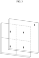
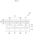
- FIG. 3 is a schematic top plan view of an organic CMOS image sensor according to some example embodiments and FIG. 4 is a cross-sectional view showing one example of the organic CMOS image sensor of FIG. 3 .
- an organic CMOS image sensor 300 includes a semiconductor substrate 110 integrated with photo-sensing devices 50a and 50b, a transmission transistor (not shown) and a charge storage 55, a lower insulation layer 60, a color filter layer 70, an upper insulation layer 80, and a photoelectric device 100.
- the semiconductor substrate 110 may be a silicon substrate, and is integrated with the photo-sensing devices 50a and 50b, the transmission transistor (not shown), and the charge storage 55.
- the photo-sensing devices 50a and 50b may be photodiodes.
- the charge storage 55 may be integrated in each pixel, and as shown in the drawing, the photo-sensing devices 50a and 50b may be respectively included in a blue pixel and a red pixel and the charge storage 55 may be included in a green pixel.
- the photo-sensing devices 50a and 50b sense light, the information sensed by the photo-sensing devices may be transferred by the transmission transistor, the charge storage 55 is electrically connected to the photoelectric device 100 that will be described later, and the information of the charge storage 55 may be transferred by the transmission transistor.
- a metal wire (not shown) and a pad (not shown) are formed on the semiconductor substrate 110.
- the metal wire and pad may be made of a metal having low resistivity, for example, aluminum (Al), copper (Cu), silver (Ag), and alloys thereof, but are not limited thereto.
- the metal wire and pad may be disposed under the photo-sensing device 50a and 50b.
- the lower insulation layer 60 is formed on the metal wire and the pad.
- the lower insulation layer 60 may be made of an inorganic insulating material such as a silicon oxide and/or a silicon nitride, or a low dielectric constant (low K) material such as SiC, SiCOH, SiCO, and SiOF.
- an inorganic insulating material such as a silicon oxide and/or a silicon nitride
- a low dielectric constant (low K) material such as SiC, SiCOH, SiCO, and SiOF.
- the lower insulation layer 60 has a trench exposing the charge storage 55.
- the trench may be filled with fillers.
- a color filter layer 70 is formed on the lower insulation layer 60.
- the color filter layer 70 includes a blue filter 70a formed in a blue pixel and a red filter 70b formed in a red pixel.
- a green filter is not included, but a green filter may be further included.
- the upper insulation layer 80 is formed on the color filter layer 70.
- the upper insulation layer 80 eliminates a step caused by the color filter layer 70 and smoothens the surface.
- the upper insulation layer 80 and the lower insulation layer 60 may include a contact hole (not shown) exposing a pad, and a through-hole 85 exposing the charge storage 55 of the green pixel.
- the photoelectric device 100 is formed on the upper insulation layer 80.
- the photoelectric device 100 includes the first electrode 10; the photoelectric conversion layer 30 including the first photoelectric conversion layer 31 and the second photoelectric conversion layer 32; and the second electrode 20 as described above.
- the first electrode 10, the photoelectric conversion layer 30, and the second electrode 20 are sequentially stacked (e.g., one of the elements is "on” another one of the elements), but this disclosure is not limited thereto, and for example they may be stacked in an order of the second electrode 20, the photoelectric conversion layer 30, and the first electrode 10.
- an element that is "on” another element may be directly or indirectly on the other element, above or below the other element, some combination thereof, or the like.
- the first electrode 10 and the second electrode 20 may be both light-transmitting electrodes and the photoelectric conversion layer 30 is the same as described above.
- the photoelectric conversion layer 30 may for example selectively absorb light in a green wavelength spectrum of light and may replace a color filter of a green pixel.
- Light in a green wavelength spectrum of light that enters from the second electrode 20 is mainly absorbed by the photoelectric conversion layer 30 and photoelectrically converted and light in a remaining wavelength spectrum of light is transmitted through the first electrode 10 and is sensed by the photo-sensing devices 50a and 50b.
- Focusing lens (not shown) may be further formed on the photoelectric device 100.
- the focusing lens may control a direction of incident light and gather the light in one region.
- the focusing lens may have a shape of, for example, a cylinder or a hemisphere, but is not limited thereto.
- the photoelectric device 100 has a stack structure thereby a size of an image sensor may be reduced to realize a down-sized image sensor.
- optical properties, electrical properties, and thermal properties required for the image sensor may be satisfied by including the photoelectric device 100 including the photoelectric conversion layer 30 having optical properties, electrical characteristics and high heat resistance.
- FIG. 4 exemplarily shows a structure that the photoelectric device of FIG. 1 is stacked, but the photoelectric device of FIG. 2 may be equally applied thereto.
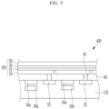
- FIG. 5 is a cross-sectional view showing another example of the organic CMOS image sensor.
- the organic CMOS image sensor 400 includes a semiconductor substrate 110 integrated with photo-sensing devices 50a and 50b, a transmission transistor (not shown), and a charge storage 55, an upper insulation layer 80 having a through-hole 85, and a photoelectric device 100, like some example embodiments.
- the photo-sensing devices 50a and 50b are stacked in a vertical direction, and the color filter layer 70 is omitted.
- the photo-sensing devices 50a and 50b are electrically connected to charge storage (not shown) and may be transferred by the transmission transistor.
- the photo-sensing devices 50a and 50b may selectively absorb light in each wavelength spectrum of light depending on a stacking depth.
- Focusing lens (not shown) may be further formed on the photoelectric device 100.
- the focusing lens may control a direction of incident light and gather the light in one region.
- the focusing lens may have a shape of, for example, a cylinder or a hemisphere, but is not limited thereto.
- the photoelectric device configured to selectively absorb light in a green wavelength spectrum of light has a stack structure and the red photo-sensing device and the blue photo-sensing device are stacked and thus the size of an image sensor may be reduced to realize a down-sized image sensor.
- FIG. 5 exemplarily shows a structure that the photoelectric device of FIG. 1 is stacked, but the photoelectric device of FIG. 2 may be equally applied thereto.
- FIG. 6 is a schematic top plan view of an organic CMOS image sensor according to some example embodiments and FIG. 7 is a cross-sectional view of the organic CMOS image sensor of FIG. 6 .
- the organic CMOS image sensor 500 includes a green photoelectric device configured to selectively absorb light in a green wavelength spectrum of light, a blue photoelectric device configured to selectively absorb light in a blue wavelength spectrum of light, and a red photoelectric device configured to selectively absorb light in a red wavelength spectrum of light, and they are stacked.
- the organic CMOS image sensor 500 includes a semiconductor substrate 110, a lower insulation layer 60, an intermediate insulation layer 65, an upper insulation layer 80, a first photoelectric device 100a, a second photoelectric device 100b, and a third photoelectric device 100c.
- the semiconductor substrate 110 may be a silicon substrate, and is integrated with the transmission transistor (not shown) and the charge storages 55a, 55b, and 55c.
- a metal wire (not shown) and a pad (not shown) are formed on the semiconductor substrate 110, and the lower insulation layer 60 is formed on the metal wire and the pad.
- the first photoelectric device 100a is formed on the lower insulation layer 60.
- the first photoelectric device 100a includes a first electrode 10a and a second electrode 20a facing each other and a photoelectric conversion layer 30a between the first electrode 10a and the second electrode 20a.
- the first electrode 10a, the second electrode 20a, and the photoelectric conversion layer 30a are the same as described above and the photoelectric conversion layer 30a may selectively absorb light in one of red, blue, and green wavelength spectrum of lights.
- the first photoelectric device 100a may be a red photoelectric device.
- the first electrode 10a, the photoelectric conversion layer 30a, and the second electrode 20a are sequentially stacked, but this disclosure is not limited thereto, and for example they may be stacked in an order of the second electrode 20a, the photoelectric conversion layer 30a, and the first electrode 10a.
- An intermediate insulation layer 65 is formed on the first photoelectric device 100a.
- the second photoelectric device 100b is formed on the intermediate insulation layer 65.
- the second photoelectric device 100b includes a first electrode 10b and a second electrode 20b facing each other and photoelectric conversion layer 30b between the first electrode 10b and the second electrode 20b.
- the first electrode 10b, the second electrode 20b, and the photoelectric conversion layer 30b may be described above and the photoelectric conversion layer 30b may selectively absorb light in one of red, blue, and green wavelength spectrum of lights.
- the second photoelectric device 100b may be a blue photoelectric device.
- the first electrode 10b, the photoelectric conversion layer 30b, and the second electrode 20b are sequentially stacked, but this disclosure is not limited thereto, and for example they may be stacked in an order of the second electrode 20b, the photoelectric conversion layer 30b, and the first electrode 10b.
- the upper insulation layer 80 is formed on the second photoelectric device 100b.
- the lower insulation layer 60, the intermediate insulation layer 65, and the upper insulation layer 80 have a plurality of through-holes exposing the charge storages 55a, 55b, and 55c.
- the third photoelectric device 100c is formed on the upper insulation layer 80.
- the third photoelectric device 100c includes a first electrode 10c and a second electrode 20c facing each other and a photoelectric conversion layer 30c between the first electrode 10c and the second electrode 20c.
- the first electrode 10c, the second electrode 20c, and the photoelectric conversion layer 30c are the same as described above and the photoelectric conversion layers 30c may selectively absorb light in one of red, blue, and green wavelength spectrum of lights.
- the third photoelectric device 100c may be a green photoelectric device and the photoelectric device 100 may be applied.
- the first electrode 10c, the photoelectric conversion layer 30c, and the second electrode 20c are sequentially stacked, but this disclosure is not limited thereto, and for example they may be stacked in an order of the second electrode 20c, the photoelectric conversion layer 30c, and the first electrode 10c.
- Focusing lens (not shown) may be further formed on the photoelectric device 100c.
- the focusing lens may control a direction of incident light and gather the light in one region.
- the focusing lens may have a shape of, for example, a cylinder or a hemisphere, but is not limited thereto.
- the photoelectric device of FIG. 1 is exemplified but the photoelectric device of FIG. 2 may be applied in the same manner.
- the first photoelectric device 100a, the second photoelectric device 100b, and the third photoelectric device 100c are sequentially stacked, but the present disclosure is not limited thereto, and they may be stacked in various orders.
- the first photoelectric device 100a, the second photoelectric device 100b, and the third photoelectric device 100c have a stack structure, and thus the size of an image sensor may be reduced to realize a down-sized image sensor.
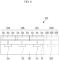
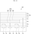
- FIG. 8 is a schematic cross-sectional view showing an organic CMOS image sensor according to some example embodiments.
- an organic CMOS image sensor 800 may include a plurality of photoelectric devices 100a, 100b, and 100c on a semiconductor substrate 110, where the plurality of photoelectric devices 100a, 100b, and 100c are configured to convert different ones of blue light, green light, or red light into electric signals, respectively.
- the organic CMOS image sensor 800 may further include an infrared/near-infrared photoelectric device 100IR.
- an organic CMOS image sensor 800 includes a semiconductor substrate 110 integrated with an a first charge storage 55a, a second charge storage 55b, a third charge storage 55c, optionally an infrared light/near infrared light charge storage 55IR, and a transmission transistor (not shown), an intermediate insulation layer 65, a first (e.g., blue) photoelectric device 100a, a second (e.g., green) photoelectric device 100b, a third (e.g., red) photoelectric device 100c, and optionally an infrared/near infrared photoelectric device 100IR.
- a first (e.g., blue) photoelectric device 100a e.g., a second (e.g., green) photoelectric device 100b
- a third (e.g., red) photoelectric device 100c e.g., and optionally an infrared/near infrared photoelectric device 100IR.
- the semiconductor substrate 110 may be a silicon substrate and may be integrated with the first charge storage 55a, the second charge storage 55b, the third charge storage 55c, optionally the infrared light/near infrared light charge storage 55IR, and the transmission transistor (not shown).
- the first charge storage 55a, the second charge storage 55a, and the third charge storage 55c may be respectively integrated in each of a blue pixel, a green pixel, and a red pixel.
- Metal wires (not shown) and pads (not shown) are formed on the semiconductor substrate 110.
- the metal wires and pads may be made of a metal having low resistivity, for example, aluminum (Al), copper (Cu), silver (Ag), and alloys thereof, but are not limited thereto.
- the intermediate insulation layer 65 may be formed on the metal wires and pads.
- the intermediate insulation layer 65 may be made of an inorganic insulation material such as a silicon oxide and/or a silicon nitride, or a low dielectric constant (low K) material such as SiC, SiCOH, SiCO, and SiOF.
- the first photoelectric device 100a, the second photoelectric device 100b, the third photoelectric device 100c, and the infrared/near infrared photoelectric device 100IR may be formed on the intermediate insulation layer 65.
- the first photoelectric device 100a includes a first electrode 10a, a second electrode 20a, and a photoelectric conversion layer 30a selectively absorbing light in a first (e.g., blue) wavelength spectrum of light
- the second photoelectric device 100b includes a first electrode 10b, a second electrode 20b and a photoelectric conversion layer 30b selectively absorbing light in a second (e.g., green) wavelength spectrum of light
- the third photoelectric device 100c includes a first electrode 10c, a second electrode 20c, and a photoelectric conversion layer 30c selectively absorbing light in a third (e.g., red) wavelength spectrum of light
- the infrared/near infrared photoelectric device 100IR includes a first electrode 10IR, a second electrode 20IR, and a photoelectric conversion layer
- the first electrodes 10a, 10b, 10c, and 10IR and the second electrodes 20a, 20b, 20c, and 20IR may be light-transmitting electrodes and may be made of, for example, a transparent conductor such as indium tin oxide (ITO), indium zinc oxide (IZO), zinc oxide (ZnO), tin oxide (SnO), aluminum tin oxide (AITO), and fluorine-doped tin oxide (FTO), or may be a metal thin layer having a thin thickness of several nanometers to several tens of nanometers or a metal thin layer having a thin thickness of several nanometers to several tens of nanometers doped with a metal oxide.
- ITO indium tin oxide
- IZO indium zinc oxide
- ZnO zinc oxide
- tin oxide SnO
- AITO aluminum tin oxide
- FTO fluorine-doped tin oxide
- FTO fluorine-doped tin oxide
- the photoelectric conversion layers 30a, 30b, 30c, and 30IR may include a p-type semiconductor material and an n-type semiconductor material.
- the photoelectric conversion layer 30a of the first photoelectric device 100a may include a p-type semiconductor material selectively absorbing light in a first (e.g., blue) wavelength spectrum of light and an n-type semiconductor material selectively absorbing light in a first (e.g., blue) wavelength spectrum of light
- the photoelectric conversion layer 30b of the second photoelectric device 100b may include a p-type semiconductor material selectively absorbing light in a second (e.g., green) wavelength spectrum of light and an n-type semiconductor material selectively absorbing light in a second (e.g., green) wavelength spectrum of light
- the photoelectric conversion layer 30c of the third photoelectric device 100c may include a p-type semiconductor material selectively absorbing light in a third (e.g., red) wavelength spectrum of light and an n-type semiconductor material selectively absorbing light in a
- the infrared/near infrared photoelectric device 100IR may selectively absorb light in an infrared wavelength spectrum of light of greater than or equal to about 700 nm and less than or equal to about 1300 nm without absorption in a visible wavelength spectrum of light.
- FIGS. 9 and 10 are schematic cross-sectional views of an organic CMOS image sensor according to some example embodiments.
- an organic CMOS image sensor 900 includes a semiconductor substrate 110 integrated with an infrared light/near infrared light charge storage 55IR, a first charge storage 55a, a second charge storage 55b, a third charge storage 55c, and a transmission transistor (not shown), an intermediate insulation layer 65, a first photoelectric device 100a, a second photoelectric device 100b, a third photoelectric device 100c, and an infrared/near infrared photoelectric device 100IR.
- the infrared/near infrared photoelectric device 100IR is formed on an entire surface of the first photoelectric device 100a, the second photoelectric device 100b, and the third photoelectric device 100c. Other structures are the same as the image sensor of FIG. 8 .
- the infrared/near infrared photoelectric device 100IR may be disposed on the intermediate insulation layer 65 and the first photoelectric device 100a, the second photoelectric device 100b, and the third photoelectric device 100c may be disposed thereon.
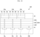
- An organic CMOS image sensor 1000 having such a structure is shown in FIG. 10 .
- the infrared/near infrared photoelectric device 100IR may selectively absorb light in an infrared wavelength spectrum of light of greater than or equal to about 700 nm and less than or equal to about 1300 nm without absorption in a visible wavelength spectrum of light and may improve efficiency due to a large absorption area.
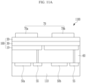
- FIG. 11A is a schematic cross-sectional view of an organic CMOS image sensor according to some example embodiments.
- an organic CMOS image sensor 1100 includes a semiconductor substrate 110 integrated with photo-sensing devices 50a and 50b, a transmission transistor (not shown) and a charge storage 55, an insulation layer 60, a color filter layer 70, and a photoelectric device 100.
- the photoelectric device 100 may be between the semiconductor substrate 110 and the color filter layer 70, such that the color filter layer 70 is distal from the photo-sensing device 50a and 50b in relation to the photoelectric device 100.
- the color filter layer 70 may include color filters configured to filter mixed wavelength spectra of light (e.g., mixed colors).
- color filter 70a may be configured to filter cyan light and color filter 70b may be configured to filter yellow light
- photoelectric device 100 may be configured to filter green light in addition to sensing green light
- photo-sensing device 50a may be configured to detect (“sense") blue light
- photo-sensing device 50b may be configured to detect red light.
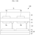
- FIG. 11B is a schematic cross-sectional view of an organic CMOS image sensor according to some example embodiments.
- an organic CMOS image sensor 1100 includes a semiconductor substrate 110 integrated with photo-sensing devices 50a and 50b, a transmission transistor (not shown) and a charge storage 55, a lower insulation layer 65, a color filter layer 70, and an upper insulation layer 88 on the semiconductor substrate 110, and a photoelectric device 100 under the semiconductor substrate 110.
- the photoelectric device 100 may be on (e.g., above or beneath) the semiconductor substrate 110, such that the color filter layer 70 is distal from the photoelectric device 100 in relation to the photo-sensing devices 50a and 50b.
- Other structures are the same as the image sensor of FIG. 4 .
- FIG. 12 is a schematic cross-sectional view of an organic CMOS image sensor according to some example embodiments.
- an organic CMOS image sensor 1200 includes a semiconductor substrate 110 integrated with an infrared light/near infrared light charge storage 55IR, a first charge storage 55a, a second charge storage 55b, a third charge storage 55c and a transmission transistor (not shown); a lower insulation layer 65; an upper insulation layer 85; a first photoelectric device 100a, a second photoelectric device 100b, a third photoelectric device 100c, an infrared/near infrared photoelectric device 100IR, a first (e.g., blue) filter 70a, a second (e.g., green) filter 70b, and a third (e.g., red) filter 70c.
- a first (e.g., blue) filter 70a e.g., blue) filter 70a
- a second (e.g., green) filter 70b e.g., red) filter 70c.
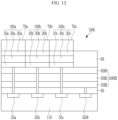
- FIG. 13 is a schematic cross-sectional view of an organic CMOS image sensor according to some example embodiments.
- an organic CMOS image sensor 1300 includes a semiconductor substrate 110 integrated with an infrared light/near infrared light charge storage 55IR, a first charge storage 55a, a second charge storage 55b, a third charge storage 55c and a transmission transistor (not shown); a lower insulation layer 65; an upper insulation layer 85; a first photoelectric device 100a, a second photoelectric device 100b, a third photoelectric device 100c, an infrared/near infrared photoelectric device 100IR, a first (e.g., blue) filter 70a, a second (e.g., green) filter 70b, and a third (e.g., red) filter 70c.
- a first (e.g., blue) filter 70a e.g., blue) filter 70a
- a second (e.g., green) filter 70b e.g., red) filter 70c.
- FIG. 14 is a schematic cross-sectional view of an organic CMOS image sensor according to some example embodiments.
- an organic CMOS image sensor 1400 includes a semiconductor substrate 110 integrated with an infrared light/near infrared light charge storage 55IR, a first charge storage 55a, a second charge storage 55b, a third charge storage 55c and a transmission transistor (not shown); a lower insulation layer 65; an upper insulation layer 85, a first (e.g., blue) filter 70a; a second (e.g., red) filter 70b; a upper insulation layers 85a and 85b; a third (e.g., green) photoelectric device 100b; and an infrared/near infrared photoelectric device 100IR.
- a first (e.g., blue) filter 70a e.g., blue) filter 70a
- a second (e.g., red) filter 70b e.g., red
- a third (e.g., green) photoelectric device 100b e.g., green
- FIG. 15 is a schematic cross-sectional view of an organic CMOS image sensor according to some example embodiments.
- the first photo-sensing device 50a e.g., a blue photodiode
- the second photo-sensing device 50b e.g., a red photodiode
- FIG. 16 is a schematic cross-sectional view of an organic CMOS image sensor according to some example embodiments.
- an organic CMOS image sensor 1600 includes a semiconductor substrate 110 integrated with an infrared light/near infrared light charge storage 55IR, a first charge storage 55a, a second charge storage 55b, a third charge storage 55c and a transmission transistor (not shown); a lower insulation layer 65; an upper insulation layer 85; a first (e.g., blue) filter 70a; a second (e.g., red) filter 70b; upper insulation layers 85a, 85b, and 85c; an infrared/near infrared photoelectric device 100IR; and a third (e.g., green) photoelectric device 100c.
- FIG. 17 is a schematic cross-sectional view of an organic CMOS image sensor according to some example embodiments.
- the first photo-sensing device 50a and the second photo-sensing device 50b are stacked perpendicularly, differing from the organic CMOS image sensor 1600 of FIG 16 .
- one or more of the photoelectric devices included in any one of the image sensors illustrated in FIGS. 3-17 may be any of the example embodiments of photoelectric devices as described herein, including photoelectric devices including photoelectric conversion layers including any of the p-type semiconductors and any of the n-type semiconductors as described with regard to any of the example embodiments described herein.
- the photoelectric device and the image sensor may be applied to various electronic devices, for example a mobile phone or a digital camera, but are not limited thereto.
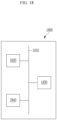
- FIG. 18 is a schematic diagram of an electronic device 1800 according to some example embodiments.
- an electronic device 1800 may include a processor 1820, a memory 1830, and an image sensor 1840 that are electrically coupled together via a bus 1810.
- the image sensor 1840 may be an image sensor of any of the example embodiments as described herein.
- the memory 1830 which may be a non-transitory computer readable medium, may store a program of instructions.
- the processor 1820 may execute the stored program of instructions to perform one or more functions.
- the processor 1820 may be configured to process electric signals generated by the image sensor 1840.
- the processor 1820 may be configured to generate an output (e.g., an image to be displayed on a display interface) based on processing the electric signals.
- 2-iodoselenophene is synthesized in a method described in Efficient Synthesis of 2-lodo and 2-Dicyanomethyl Derivatives of Thiophene, Selenophene, Tellurophene and Thieno[3,2-b]thiophene, Takahashi, K.; Tarutani, S. Heterocycles 1996, 43, 1927-1935 .
- 10H-phenoselenazine is purchased from Medigen Inc. (purity: 98 % or greater). Reference about a method of synthesizing 10H-phenoselenazine: Preparation and Some Reactions of Phenoxazine and Phenoselenazine, Paulette Mller, N. P. Buu- HI and R. RIPS, J. Org. Chem., 1959, 24 1, pp 37-39 .
- a resultant therefrom is washed with n-hexane to obtain a crude product.
- the crude product is moved into a 2 L triangular flask, 450 ml of chloroform is added thereto, and the obtained mixture is heated and stirred at 70 °C to dissolve the product.
- 700 ml of n-hexane is slowly added thereto drop by drop, and the obtained mixture is cooled down to room temperature and filtered to obtain a product.
- the precipitation and purification are repeated up to purity of 99.9 %.
- the product is vacuum-dried at 150 °C for 2 hours to remove residual hexane to obtain 3.02 g of (Z)-6-((5-(10H-phenoselenazin-10-yl)selenophen-2-yl)methylene)-5H-indeno[5,6-b]selenophene-5,7(6H)-dione.
- the product may be purified by being baked at 150 °C for greater than or equal to 2 hours to sublime.
- a yield is 83 %.
- Compound (1) is synthesized according to the method described in Heterocycles 2008, 75, 11, 2735-2744 and Pharmazie 198439 10, 671-2 .
- 2-iodoselenophene is synthesized in a method described in Efficient Synthesis of 2-lodo and 2-Dicyanomethyl Derivatives of Thiophene, Selenophene, Tellurophene and Thieno[3,2-b]thiophene, Takahashi, K.; Tarutani, S. Heterocycles 1996, 43, 1927-1935 .
- 0.16 ml of phosphoryl chloride is added in a dropwise fashion to 0.5 ml of N,N-dimethylformamide at -15 °C, and the mixture is stirred at room temperature (24 °C) for 2 hours.
- the resultant is slowly added in a dropwise fashion to 10 ml of dichloromethane and 0.46 g (1.54 mmol) of Compound 3 at -15 °C, and the obtained mixture is stirred at room temperature for 30 minutes and concentrated under a reduced pressure. Subsequently, 5 ml of water was added thereto, a sodium hydroxide aqueous solution is added thereto until pH becomes 14, and the resulting mixture is stirred at room temperature (24 °C) for 2 hours.
- a 150 nm-thick anode is formed by sputtering ITO on a glass substrate and a 5 nm-thick charge auxiliary layer is formed by depositing compound represented by Chemical Formula A thereon. Subsequently, on the charge auxiliary layer, a 50 nm-thick first photoelectric conversion layer is formed by codepositing the compound represented by Chemical Formula A-1 obtained in Synthesis Example 1 (first p-type semiconductor 33) and C60 (first n-type semiconductor 35) in a volume ratio of 1.3:1.
- a 50 nm-thick second photoelectric conversion layer is formed by codepositing the compound represented by Chemical Formula A-3 obtained in Synthesis Example 3 (second p-type semiconductor 37) and C60 (second n-type semiconductor 39) in a volume ratio of 2:1.
- a 7 nm-thick cathode is formed by sputtering ITO.
- a 50 nm-thick anti-reflection layer is formed by depositing aluminum oxide (Al 2 O 3 ), and a glass plate is used for sealing to manufacture a photoelectric device.
- a photoelectric device is manufactured according to the same method as Example 1 except that the first photoelectric conversion layer has a thickness of 30 nm and the second photoelectric conversion layer has a thickness of 70 nm.
- a photoelectric device is manufactured according to the same method as Example 1 except that the first photoelectric conversion layer has a thickness of 10 nm and the second photoelectric conversion layer has a thickness of 90 nm.
- a 150 nm-thick anode is formed by sputtering ITO on a glass substrate and a 5 nm-thick charge auxiliary layer is formed by depositing compound represented by Chemical Formula A thereon.
- a 100 nm-thick single photoelectric conversion layer is formed by codepositing the compound represented by Chemical Formula A-1 obtained in Synthesis Example 1 (p-type semiconductor) and C60 (n-type semiconductor) in a volume ratio of 1.3:1.
- a 7 nm-thick cathode is formed by sputtering ITO.
- a 50 nm-thick anti-reflection layer is formed by depositing aluminum oxide (Al 2 O 3 ), and a glass plate is used for sealing to manufacture a photoelectric device.
- a 150 nm-thick anode is formed by sputtering ITO on a glass substrate and a 5 nm-thick charge auxiliary layer is formed by depositing Compound represented by Chemical Formula A thereon. Subsequently, on the charge auxiliary layer, a 50 nm-thick first photoelectric conversion layer is formed by codepositing the compound represented by Chemical Formula A-2 obtained in Synthesis Example 2 (first p-type semiconductor) and C60 (first n-type semiconductor) in a volume ratio of 1:1.
- a 50 nm-thick second photoelectric conversion layer is formed by codepositing the compound represented by Chemical Formula A-3 obtained in Synthesis Example 3 (second p-type semiconductor) and C60 (second n-type semiconductor) in a volume ratio of 2:1.
- a 7 nm-thick cathode is formed by sputtering ITO.
- a 50 nm-thick anti-reflection layer is formed by depositing aluminum oxide (Al 2 O 3 ), and a glass plate is used for sealing to manufacture a photoelectric device.
- a photoelectric device is manufactured according to the same method as Example 4 except that the first photoelectric conversion layer has a thickness of 30 nm and the second photoelectric conversion layer has a thickness of 70 nm.
- a photoelectric device is manufactured according to the same method as Example 4 except that the first photoelectric conversion layer has a thickness of 10 nm and the second photoelectric conversion layer has a thickness of 90 nm.
- a 150 nm-thick anode is formed by sputtering ITO on a glass substrate and a 5 nm-thick charge auxiliary layer is formed by depositing compound represented by Chemical Formula A thereon.
- a 100 nm-thick single photoelectric conversion layer is formed by codepositing the compound represented by Chemical Formula A-2 obtained in Synthesis Example 2 (p-type semiconductor) and C60 (n-type semiconductor) in a volume ratio of 1.1:1.
- a 7 nm-thick cathode is formed by sputtering ITO.
- a 50 nm-thick anti-reflection layer is formed by depositing aluminum oxide (Al 2 O 3 ), and a glass plate is used for sealing to manufacture a photoelectric device.
- a 150 nm-thick anode is formed by sputtering ITO on a glass substrate and a 5 nm-thick charge auxiliary layer is formed by depositing compound represented by Chemical Formula A thereon.
- a 100 nm-thick single photoelectric conversion layer is formed by codepositing the compound represented by Chemical Formula A-3 obtained in Synthesis Example 3 (p-type semiconductor) and C60(n-type semiconductor) in a volume ratio of 2:1.
- a 7 nm-thick cathode is formed by sputtering ITO.
- a 50 nm-thick anti-reflection layer is formed by depositing aluminum oxide (Al 2 O 3 ), and a glass plate is used for sealing to manufacture a photoelectric device.
- the photoelectric devices according to Examples 1 to 3 exhibit narrow light-absorption full widths at half maximum (FWHM) compared with the photoelectric device according to Comparative Example 1, and from the results, the photoelectric devices according to Examples 1 to 3 have wavelength selectivity compared with the photoelectric device according to Comparative Example 1.
- FWHM full widths at half maximum
- the photoelectric devices according to Examples 4 to 6 exhibit narrow light-absorption full widths at half maximum (FWHM) compared with the photoelectric device according to Comparative Example 2, and from the results, the photoelectric devices according to Examples 4 to 6 have wavelength selectivity compared with the photoelectric device according to Comparative Example 2.
- FWHM full widths at half maximum
- the peak absorption wavelengths ⁇ max1 and the light-absorption FWHMs of the first photoelectric conversion layers in the photoelectric devices of Examples 1 to 3 are equal to the peak absorption wavelength and the light-absorption FWHM of the photoelectric device of Comparative Example 1, respectively.
- the peak absorption wavelengths ⁇ max1 and the light-absorption FWHMs of the first photoelectric conversion layers in the photoelectric devices of Examples 4 to 6 are equal to the peak absorption wavelength and the light-absorption FWHM of the photoelectric device of Comparative Example 2, respectively.
- the peak absorption wavelengths ⁇ max2 and the light-absorption FWHMs of the second photoelectric conversion layers in the photoelectric devices of Examples 1 to 6 are equal to the peak absorption wavelength and the light-absorption FWHM of the photoelectric device of Comparative Example 3, respectively.
- the external quantum efficiency (EQE) is evaluated at 3V at a peak absorption wavelength ( ⁇ max ) and at a wavelength of 450 nm using an Incident Photon to Current Efficiency (IPCE) method.
- the photoelectric devices according to Examples 1 to 3 exhibit a high ratio of external quantum efficiency at a peak absorption wavelength ( ⁇ max ) to external quantum efficiency at a wavelength of 450 nm compared with the photoelectric device according to Comparative Example 1, and from the results, the photoelectric devices according to Examples 1 to 3 have a better wavelength selectivity compared with the photoelectric device according to Comparative Example 1.
- the photoelectric devices according to Examples 4 to 6 exhibit a high ratio of external quantum efficiency at a peak absorption wavelength ( ⁇ max ) to external quantum efficiency at a wavelength of 450 nm compared with the photoelectric device according to Comparative Example 2, and from the results, the photoelectric devices according to Examples 4 to 6 have a better wavelength selectivity compared with the photoelectric device according to Comparative Example 2.
- the thermal resistance properties are measured by variation ratios of the external quantum efficiency (EQE) after placing the photoelectric devices according to Examples 1 to 6 and Comparative Example 3 at 170 °C for 3 hours.
- EQE external quantum efficiency
- the photoelectric devices according to Examples 1 to 6 exhibit small changes of the external quantum efficiency after placing them at a high temperature, indicating a higher thermal resistance, compared with the photoelectric device according to Comparative Example 3.
- Image sensors including the photoelectric devices according to Examples and Comparative Examples having structure shown in FIGS. 3 and 4 are designed and optical cross-talk (C.T) of each image sensor is measured.
- C.T optical cross-talk
- the optical cross-talk is evaluated by dividing a visible ray wavelength spectrum of light into three regions of greater than or equal to about 400 nm and less than about 440 nm (blue), about 520 nm to 560 nm (green), and greater than about 630 nm and less than or equal to about 670 nm and then, evaluating how much other light conversion devices in each region are optically interfered.
- optical cross-talk in a green wavelength spectrum of light is indicated by a relative integral of sensitivity curves of the blue photoelectric device and the red photoelectric device in 520 nm to 560 nm when an integral of sensitivity curve of the green photoelectric device in 520 nm to 560 nm is 100.
- optical cross-talk As the optical cross-talk is smaller, cross-talk of the image sensors are lowered and color mixing in a green wavelength spectrum of light is decreased.
- the image sensors including photoelectric devices according to Examples exhibit smaller optical cross-talk compared with the image sensors including the photoelectric device according to Comparative Examples.
- Image sensors including the photoelectric devices according to Examples and Comparative Examples having structure shown in FIGS. 3 and 4 are designed and color differences of each image sensor are measured.
- the color difference of the image sensor is evaluated in the following method.
- a RGB raw signal obtained from the image sensor is image-processed to reduce a difference from a real color.
- the image processing includes a white balance process of unifying intensity of the RGB raw signal and a color correction process of reducing a color difference between an actual color of Macbeth chart (24 colors) and a primary color obtained from the image sensor.
- the color correction process expresses a color by converting the RGB raw signal measured from the image sensor through a color correction matrix (CCM), and color characteristics of the image sensor may be evaluated by digitalizing a color difference of the converted color from the actual color of the Macbeth chart.
- CCM color correction matrix
- the color difference indicates a difference from an actual color in the Macbeth chart, and as the color difference is smaller, a color may be closer to the actual color.
- image sensors including the photoelectric device according to Examples exhibit smaller color difference compared with image sensors including the photoelectric device according to Comparative Examples.
- the image sensors including the photoelectric device according to some example embodiments will show improved color reproducibility compared with the image sensors including the photoelectric device according to Comparative Examples.
Landscapes
- Physics & Mathematics (AREA)
- Chemical & Material Sciences (AREA)
- Engineering & Computer Science (AREA)
- Materials Engineering (AREA)
- Electromagnetism (AREA)
- Spectroscopy & Molecular Physics (AREA)
- Nanotechnology (AREA)
- Inorganic Chemistry (AREA)
- Light Receiving Elements (AREA)
- Solid State Image Pick-Up Elements (AREA)
Claims (15)
- Fotoelektrische Vorrichtung, umfassend:eine erste Elektrode (10),eine erste fotoelektrische Umwandlungsschicht (31) auf der ersten Elektrode (10), wobei die erste fotoelektrische Umwandlungsschicht (31) einen ersten Heteroübergang beinhaltet, der einen ersten Halbleiter vom p-Typ und einen ersten Halbleiter vom n-Typ beinhaltet,eine zweite fotoelektrische Umwandlungsschicht (32) auf der ersten fotoelektrischen Umwandlungsschicht (31), wobei die zweite fotoelektrische Umwandlungsschicht (32) einen zweiten Heteroübergang beinhaltet, der einen zweiten Halbleiter vom p-Typ und einen zweiten Halbleiter vom n-Typ beinhaltet, undeine zweite Elektrode (20) auf der zweiten fotoelektrischen Umwandlungsschicht (32),wobei die erste fotoelektrische Umwandlungsschicht (31) einer ersten Spitzenabsorptionswellenlänge (λmax1) zugeordnet ist, die zweite fotoelektrische Konversionsschicht (32) einer zweiten Spitzenabsorptionswellenlänge (λmax2) zugeordnet ist und sowohl die erste Spitzenabsorptionswellenlänge als auch die zweite Spitzenabsorptionswellenlänge in einem gemeinsamen Wellenlängenspektrum des Lichts enthalten sind, wobei das gemeinsame Wellenlängenspektrum des Lichts ein Wellenlängenspektrum des Lichts von 510 nm bis 560 nm ist,wobei eine Halbwertsbreite (Full Width at Half Maximum - FWHM) der Lichtabsorption der zweiten fotoelektrischen Umwandlungsschicht (32) schmaler als eine FWHM der Lichtabsorption der ersten fotoelektrische Umwandlungsschicht (31) ist undwobei die FWHM der zweiten fotoelektrischen Umwandlungsschicht (32) kleiner als oder gleich 110 nm ist.
- Fotoelektrische Vorrichtung nach Anspruch 1, wobei ein Extinktionskoeffizient bei der zweiten Spitzenabsorptionswellenlänge (λmax2) der zweiten fotoelektrischen Umwandlungsschicht gleich oder größer als ein Extinktionskoeffizient bei der ersten Spitzenabsorptionswellenlänge (λmax1) der ersten fotoelektrischen Umwandlungsschicht ist.
- Fotoelektrische Vorrichtung nach Anspruch 1 oder 2, wobei die externe Quanteneffizienz bei der zweiten Spitzenabsorptionswellenlänge (λmax2) der zweiten fotoelektrischen Umwandlungsschicht gleich oder größer als die externe Quanteneffizienz bei der ersten Spitzenabsorptionswellenlänge (λmax1) der ersten fotoelektrischen Umwandlungsschicht ist.
- Fotoelektrische Vorrichtung nach einem der Ansprüche 1 bis 3, wobei eine FWHM der Lichtabsorption des zweiten Halbleiters vom p-Typ schmaler als eine FWHM der Lichtabsorption des ersten Halbleiters vom p-Typ ist.
- Fotoelektrische Vorrichtung nach einem der Ansprüche 1 bis 4, wobei der erste Halbleiter vom n-Typ und der zweite Halbleiter vom n-Typ jeweils separat Fulleren oder ein Fullerenderivat enthalten.
- Fotoelektrische Vorrichtung nach einem der Ansprüche 1 bis 5, wobei die fotoelektrische Vorrichtung ferner Folgendes umfasst:eine Ladungshilfsschicht mindestens zwischender ersten Elektrode und der ersten fotoelektrischen Umwandlungsschicht oderzwischen der zweiten Elektrode und der zweiten fotoelektrischen Umwandlungsschicht,wobei die Ladungshilfsschicht dazu konfiguriert ist, Licht in einem sichtbaren Wellenlängenspektrum des Lichts im Wesentlichen nicht zu absorbieren.
- Fotoelektrische Vorrichtung nach einem der Ansprüche 1 bis 6, wobei die Ladungsbeweglichkeit der ersten fotoelektrischen Umwandlungsschicht größer als die Ladungsbeweglichkeit der zweiten fotoelektrischen Umwandlungsschicht ist.
- Fotoelektrische Vorrichtung nach Anspruch 7, wobei die Ladungsbeweglichkeit des ersten Halbleiters vom p-Typ größer als die Ladungsbeweglichkeit des zweiten Halbleiters vom p-Typ ist; und/oder
wobei ein HOMO-Energieniveau des ersten Halbleiters vom p-Typ flacher als ein HOMO-Energieniveau des zweiten Halbleiters vom p-Typ ist. - Fotoelektrische Vorrichtung nach einem der Ansprüche 1 bis 8, wobei eine Dicke der zweiten fotoelektrischen Umwandlungsschicht gleich oder größer als eine Dicke der ersten fotoelektrischen Umwandlungsschicht ist;
wobei vorzugsweise das Dickenverhältnis der ersten fotoelektrischen Umwandlungsschicht und der zweiten fotoelektrischen Umwandlungsschicht 50:50 bis 5:95 beträgt. - Fotoelektrische Vorrichtung nach einem der Ansprüche 1 bis 9, wobei die zweite Spitzenabsorptionswellenlänge (λmax2) in einem Wellenlängenspektrum von Licht von 530 nm bis 550 nm liegt.
- Fotoelektrische Vorrichtung nach einem der Ansprüche 1 bis 10, wobei externe Quanteneffizienzen bei den jeweiligen Spitzenabsorptionswellenlängen und externe Quanteneffizienzen bei 450 nm der ersten fotoelektrischen Umwandlungsschicht und der zweiten fotoelektrischen Umwandlungsschicht die Beziehungsgleichung 1 erfüllen,
 wobei in Beziehungsgleichung 1EQE(2)λmax2 die externe Quanteneffizienz bei der zweiten Spitzenabsorptionswellenlänge (λmax2) ist,EQE(2)450nm die externe Quanteneffizienz bei einer Wellenlänge von 450 nm der zweiten fotoelektrischen Umwandlungsschicht ist,EQE(1)λmax1 die externe Quanteneffizienz bei der ersten Spitzenabsorptionswellenlänge (λmax1) ist undEQE(1)450nm die externe Quanteneffizienz bei einer Wellenlänge von 450 nm der ersten fotoelektrischen Umwandlungsschicht ist.
 - Bildsensor, umfassend die fotoelektrische Vorrichtung nach einem der Ansprüche 1 bis 11.
- Elektronische Vorrichtung, umfassend den Bildsensor nach Anspruch 12.
- Bildsensor nach Anspruch 12, umfassend:ein Halbleitersubstrat; undeine Vielzahl von fotoelektrischen Vorrichtungen nach einem der Ansprüche 1 bis 11 auf dem Halbleitersubstrat, wobei die Vielzahl von fotoelektrischen Vorrichtungen dazu konfiguriert ist, blaues Licht, grünes Licht oder rotes Licht jeweils in elektrische Signale umzuwandeln;vorzugsweise ferner umfassend:
eine fotoelektrische Infrarotvorrichtung auf dem Halbleitersubstrat, wobei die fotoelektrische Infrarotvorrichtung dazu konfiguriert ist, Infrarotlicht in elektrische Signale umzuwandeln. - Bildsensor nach Anspruch 14, wobei sich die fotoelektrische Infrarotvorrichtung auf der Vielzahl von fotoelektrischen Vorrichtungen befindet;
wobei sich die fotoelektrische Infrarotvorrichtung vorzugsweise zwischen der Vielzahl von fotoelektrischen Vorrichtungen und dem Halbleitersubstrat befindet.
Applications Claiming Priority (1)
| Application Number | Priority Date | Filing Date | Title |
|---|---|---|---|
| KR20170164147 | 2017-12-01 |
Publications (3)
| Publication Number | Publication Date |
|---|---|
| EP3493262A2 EP3493262A2 (de) | 2019-06-05 |
| EP3493262A3 EP3493262A3 (de) | 2019-11-06 |
| EP3493262B1 true EP3493262B1 (de) | 2023-09-20 |
Family
ID=64453294
Family Applications (1)
| Application Number | Title | Priority Date | Filing Date |
|---|---|---|---|
| EP18207585.3A Active EP3493262B1 (de) | 2017-12-01 | 2018-11-21 | Photoelektrische vorrichtungen und bildsensoren und elektronische vorrichtungen |
Country Status (4)
| Country | Link |
|---|---|
| US (2) | US10998514B2 (de) |
| EP (1) | EP3493262B1 (de) |
| KR (1) | KR102697766B1 (de) |
| CN (1) | CN109873011B (de) |
Families Citing this family (15)
| Publication number | Priority date | Publication date | Assignee | Title |
|---|---|---|---|---|
| US12009379B2 (en) * | 2017-05-01 | 2024-06-11 | Visera Technologies Company Limited | Image sensor |
| WO2019182143A1 (ja) * | 2018-03-23 | 2019-09-26 | 住友化学株式会社 | 光電変換素子 |
| TW202035577A (zh) * | 2018-09-06 | 2020-10-01 | 日商富士軟片股份有限公司 | 結構體、光感測器及圖像顯示裝置 |
| CN109887943B (zh) * | 2019-03-05 | 2021-01-05 | 西安工业大学 | 选择性吸收增强的宽光谱多波段探测结构及其制备方法 |
| WO2020218046A1 (ja) * | 2019-04-26 | 2020-10-29 | パナソニックIpマネジメント株式会社 | 撮像素子 |
| KR102819931B1 (ko) * | 2019-08-01 | 2025-06-11 | 삼성전자주식회사 | 센서 및 전자 장치 |
| DE102019125447A1 (de) * | 2019-09-20 | 2021-03-25 | Infineon Technologies Ag | Halbleitersubstrat mit einem Bondpat-Material auf Aluminiumbasis |
| KR102851625B1 (ko) * | 2019-11-05 | 2025-08-27 | 삼성전자주식회사 | 광전 변환 소자, 센서 및 전자 장치 |
| US11793007B2 (en) | 2019-11-05 | 2023-10-17 | Samsung Electronics Co., Ltd. | Photoelectric conversion devices and sensors and electronic devices |
| KR102851626B1 (ko) * | 2019-11-05 | 2025-08-28 | 삼성전자주식회사 | 광전 변환 소자, 센서 및 전자 장치 |
| KR102764010B1 (ko) * | 2020-04-29 | 2025-02-05 | 삼성전자주식회사 | 센서 및 전자 장치 |
| CN112164763B (zh) * | 2020-09-29 | 2023-05-26 | 京东方科技集团股份有限公司 | 有机发光显示面板、制备有机发光显示面板的方法及显示装置 |
| EP3993052B1 (de) | 2020-10-28 | 2025-03-26 | Samsung Electronics Co., Ltd. | Sensor und elektronische vorrichtung |
| CN117157275A (zh) * | 2021-04-07 | 2023-12-01 | 浙江光昊光电科技有限公司 | 化合物及其在光电领域的应用 |
| JPWO2024203386A1 (de) * | 2023-03-31 | 2024-10-03 |
Family Cites Families (21)
| Publication number | Priority date | Publication date | Assignee | Title |
|---|---|---|---|---|
| US6352777B1 (en) | 1998-08-19 | 2002-03-05 | The Trustees Of Princeton University | Organic photosensitive optoelectronic devices with transparent electrodes |
| US7667391B2 (en) | 2006-08-04 | 2010-02-23 | Eastman Kodak Company | Electrically excited organic light-emitting diodes with spatial and spectral coherence |
| JP2009088292A (ja) * | 2007-09-28 | 2009-04-23 | Fujifilm Corp | 光電変換素子、撮像素子及び光センサー |
| JP4889623B2 (ja) * | 2007-12-26 | 2012-03-07 | 三洋電機株式会社 | 透明導電膜及び透明導電膜を用いた太陽電池 |
| KR101447113B1 (ko) * | 2008-01-15 | 2014-10-07 | 삼성전자주식회사 | 화합물 반도체 수직 적층 이미지 센서 |
| JP4863096B2 (ja) | 2009-04-30 | 2012-01-25 | ブラザー工業株式会社 | 印刷システム、印刷装置及びプリンタドライバ |
| FR2949775B1 (fr) | 2009-09-10 | 2013-08-09 | Saint Gobain Performance Plast | Substrat de protection pour dispositif collecteur ou emetteur de rayonnement |
| KR101701920B1 (ko) | 2010-03-05 | 2017-02-03 | 삼성전자주식회사 | 포토다이오드 및 이의 제조 방법, 이를 이용한 광전 소자 |
| ES2857904T3 (es) * | 2010-05-04 | 2021-09-29 | Heliatek Gmbh | Componente fotoactivo con capas orgánicas |
| US9508945B2 (en) * | 2012-06-27 | 2016-11-29 | Regents Of The University Of Minnesota | Spectrally tunable broadband organic photodetectors |
| FR2999807B1 (fr) | 2012-12-13 | 2015-01-02 | Saint Gobain | Support conducteur pour dispositif oled, ainsi que dispositif oled l'incorporant |
| US9159753B2 (en) | 2013-03-01 | 2015-10-13 | Semiconductor Components Industries, Llc | Image sensor pixels with self-aligned lateral anti-blooming structures |
| KR101514207B1 (ko) | 2013-04-15 | 2015-06-05 | 한국과학기술연구원 | 낮은 밴드갭을 갖는 고분자 화합물, 이를 포함하는 유기태양전지 및 이의 제조방법 |
| WO2015042609A1 (en) | 2013-09-23 | 2015-03-26 | The Regents Of The University Of California | Multiple donor/acceptor bulk heterojunction solar cells |
| DE102013017361B4 (de) | 2013-10-18 | 2023-05-04 | Pictiva Displays International Limited | Organisches Licht emittierendes Bauelement und Verfahren zur Herstellung eines organischen Licht ermittierenden Bauelements |
| KR20150054550A (ko) | 2013-11-12 | 2015-05-20 | 이화여자대학교 산학협력단 | 복층 유기광전소자 및 그의 제조 방법 |
| TW201539819A (zh) | 2014-01-15 | 2015-10-16 | Univ Michigan | 高效率多接面小分子光伏裝置 |
| US9978951B2 (en) | 2014-03-31 | 2018-05-22 | Sony Corporation | Perylene-based materials for organic photoelectric conversion layers |
| JP6567276B2 (ja) * | 2014-05-13 | 2019-08-28 | ソニーセミコンダクタソリューションズ株式会社 | 固体撮像素子、および電子機器 |
| KR102243553B1 (ko) * | 2014-07-16 | 2021-04-22 | 삼성전자주식회사 | 유기 광전 소자 및 이미지 센서 |
| KR101636687B1 (ko) | 2014-07-21 | 2016-07-06 | 한국과학기술연구원 | 낮은 밴드갭을 갖는 고분자 화합물, 그 제조 방법 및 이를 포함하는 유기태양전지 |
-
2018
- 2018-11-02 US US16/178,691 patent/US10998514B2/en active Active
- 2018-11-21 EP EP18207585.3A patent/EP3493262B1/de active Active
- 2018-11-27 CN CN201811423995.7A patent/CN109873011B/zh active Active
- 2018-11-30 KR KR1020180153038A patent/KR102697766B1/ko active Active
-
2021
- 2021-05-03 US US17/306,116 patent/US11997856B2/en active Active
Non-Patent Citations (4)
| Title |
|---|
| ADEBANJO OLUSEGUN ET AL: "Triple junction polymer solar cells", ENERGY & ENVIRONMENTAL SCIENCE, vol. 6, no. 11, 1 January 2013 (2013-01-01), Cambridge, pages 3150, XP055860016, ISSN: 1754-5692, DOI: 10.1039/c3ee42257g * |
| FARJAMTALAB IMAN ET AL: "Current density of anodes, recombination rate and luminance in MEH-PPV, MDMO-PPV, and P3HT polymers in polymer light-emitting diodes", POLYMER SCIENCE., vol. 58, no. 5, 1 September 2016 (2016-09-01), US, pages 726 - 731, XP055860017, ISSN: 0965-545X, DOI: 10.1134/S0965545X16050059 * |
| GILOT JAN ET AL: "Double and triple junction polymer solar cells processed from solution", APPLIED PHYSICS LETTERS, AMERICAN INSTITUTE OF PHYSICS, 2 HUNTINGTON QUADRANGLE, MELVILLE, NY 11747, vol. 90, no. 14, 5 April 2007 (2007-04-05), pages 143512 - 143512, XP012094011, ISSN: 0003-6951, DOI: 10.1063/1.2719668 * |
| HARALD HOPPE ET AL: "Organic solar cells: An overview", JOURNAL OF MATERIALS RESEARCH, vol. 19, no. 7, 1 July 2004 (2004-07-01), pages 1924 - 1945, XP055000317, ISSN: 0884-2914, DOI: 10.1557/JMR.2004.0252 * |
Also Published As
| Publication number | Publication date |
|---|---|
| US11997856B2 (en) | 2024-05-28 |
| EP3493262A2 (de) | 2019-06-05 |
| US20190173032A1 (en) | 2019-06-06 |
| CN109873011B (zh) | 2023-12-26 |
| US20210273186A1 (en) | 2021-09-02 |
| US10998514B2 (en) | 2021-05-04 |
| CN109873011A (zh) | 2019-06-11 |
| KR20190065171A (ko) | 2019-06-11 |
| KR102697766B1 (ko) | 2024-08-22 |
| EP3493262A3 (de) | 2019-11-06 |
Similar Documents
| Publication | Publication Date | Title |
|---|---|---|
| EP3493262B1 (de) | Photoelektrische vorrichtungen und bildsensoren und elektronische vorrichtungen | |
| EP3509108B1 (de) | Photoelektrische vorrichtungen und bildsensoren und elektronische vorrichtungen | |
| EP2978023B1 (de) | Photoelektronisches Bildsensor | |
| US11456336B2 (en) | Organic photoelectric device and image sensor and electronic device | |
| KR102282495B1 (ko) | 화합물, 유기 광전자 소자 및 이미지 센서 | |
| JP6591190B2 (ja) | 有機光電素子及びこれを有するイメージセンサ | |
| US11437438B2 (en) | Photoelectric conversion devices and organic sensors and electronic devices | |
| US20200136063A1 (en) | Compound and film and photoelectric diode and organic sensor and electronic device | |
| US11793007B2 (en) | Photoelectric conversion devices and sensors and electronic devices | |
| US11591347B2 (en) | Compounds and films and photoelectric diodes and organic sensors and electronic devices | |
| EP3825319B1 (de) | Nahinfrarotabsorber, nahinfrarotabsorbierende/-blockierende folien, photoelektrische vorrichtungen, organische sensoren und elektronische vorrichtungen | |
| EP3643712B1 (de) | Verbindung und film sowie fotoelektrische diode und organischer sensor und elektronische vorrichtung | |
| CN111196799B (zh) | 富勒烯衍生物、以及包括其的有机光电器件、图像传感器、和电子设备 | |
| EP3819955A1 (de) | Vorrichtungen zur photoelektrischen umwandlung und sensoren und elektronische vorrichtungen | |
| KR102490615B1 (ko) | 플러렌 유도체, 광전 소자 및 이미지 센서 | |
| EP3660935A1 (de) | Photoelektrische umwandlungsvorrichtungen und organische sensoren und elektronische vorrichtungen |
Legal Events
| Date | Code | Title | Description |
|---|---|---|---|
| PUAI | Public reference made under article 153(3) epc to a published international application that has entered the european phase |
Free format text: ORIGINAL CODE: 0009012 |
|
| STAA | Information on the status of an ep patent application or granted ep patent |
Free format text: STATUS: THE APPLICATION HAS BEEN PUBLISHED |
|
| AK | Designated contracting states |
Kind code of ref document: A2 Designated state(s): AL AT BE BG CH CY CZ DE DK EE ES FI FR GB GR HR HU IE IS IT LI LT LU LV MC MK MT NL NO PL PT RO RS SE SI SK SM TR |
|
| AX | Request for extension of the european patent |
Extension state: BA ME |
|
| PUAL | Search report despatched |
Free format text: ORIGINAL CODE: 0009013 |
|
| AK | Designated contracting states |
Kind code of ref document: A3 Designated state(s): AL AT BE BG CH CY CZ DE DK EE ES FI FR GB GR HR HU IE IS IT LI LT LU LV MC MK MT NL NO PL PT RO RS SE SI SK SM TR |
|
| AX | Request for extension of the european patent |
Extension state: BA ME |
|
| RIC1 | Information provided on ipc code assigned before grant |
Ipc: H01L 27/30 20060101AFI20191002BHEP Ipc: H01L 51/46 20060101ALN20191002BHEP |
|
| STAA | Information on the status of an ep patent application or granted ep patent |
Free format text: STATUS: REQUEST FOR EXAMINATION WAS MADE |
|
| 17P | Request for examination filed |
Effective date: 20200506 |
|
| RBV | Designated contracting states (corrected) |
Designated state(s): AL AT BE BG CH CY CZ DE DK EE ES FI FR GB GR HR HU IE IS IT LI LT LU LV MC MK MT NL NO PL PT RO RS SE SI SK SM TR |
|
| STAA | Information on the status of an ep patent application or granted ep patent |
Free format text: STATUS: EXAMINATION IS IN PROGRESS |
|
| 17Q | First examination report despatched |
Effective date: 20211117 |
|
| REG | Reference to a national code |
Ref country code: DE Ref legal event code: R079 Free format text: PREVIOUS MAIN CLASS: H01L0027300000 Ipc: H10K0039320000 Ref document number: 602018057840 Country of ref document: DE |
|
| RIC1 | Information provided on ipc code assigned before grant |
Ipc: H10K 30/30 20230101ALN20230301BHEP Ipc: H10K 30/57 20230101ALN20230301BHEP Ipc: H10K 85/20 20230101ALI20230301BHEP Ipc: H10K 85/60 20230101ALI20230301BHEP Ipc: H01L 27/146 20060101ALI20230301BHEP Ipc: H10K 39/32 20230101AFI20230301BHEP |
|
| GRAP | Despatch of communication of intention to grant a patent |
Free format text: ORIGINAL CODE: EPIDOSNIGR1 |
|
| STAA | Information on the status of an ep patent application or granted ep patent |
Free format text: STATUS: GRANT OF PATENT IS INTENDED |
|
| RIC1 | Information provided on ipc code assigned before grant |
Ipc: H10K 102/10 20230101ALN20230321BHEP Ipc: H10K 30/30 20230101ALN20230321BHEP Ipc: H10K 30/57 20230101ALN20230321BHEP Ipc: H10K 85/20 20230101ALI20230321BHEP Ipc: H10K 85/60 20230101ALI20230321BHEP Ipc: H01L 27/146 20060101ALI20230321BHEP Ipc: H10K 39/32 20230101AFI20230321BHEP |
|
| INTG | Intention to grant announced |
Effective date: 20230411 |
|
| RIC1 | Information provided on ipc code assigned before grant |
Ipc: H10K 102/10 20230101ALN20230324BHEP Ipc: H10K 30/30 20230101ALN20230324BHEP Ipc: H10K 30/57 20230101ALN20230324BHEP Ipc: H10K 85/20 20230101ALI20230324BHEP Ipc: H10K 85/60 20230101ALI20230324BHEP Ipc: H01L 27/146 20060101ALI20230324BHEP Ipc: H10K 39/32 20230101AFI20230324BHEP |
|
| P01 | Opt-out of the competence of the unified patent court (upc) registered |
Effective date: 20230519 |
|
| GRAS | Grant fee paid |
Free format text: ORIGINAL CODE: EPIDOSNIGR3 |
|
| GRAA | (expected) grant |
Free format text: ORIGINAL CODE: 0009210 |
|
| STAA | Information on the status of an ep patent application or granted ep patent |
Free format text: STATUS: THE PATENT HAS BEEN GRANTED |
|
| AK | Designated contracting states |
Kind code of ref document: B1 Designated state(s): AL AT BE BG CH CY CZ DE DK EE ES FI FR GB GR HR HU IE IS IT LI LT LU LV MC MK MT NL NO PL PT RO RS SE SI SK SM TR |
|
| REG | Reference to a national code |
Ref country code: GB Ref legal event code: FG4D |
|
| REG | Reference to a national code |
Ref country code: CH Ref legal event code: EP |
|
| REG | Reference to a national code |
Ref country code: IE Ref legal event code: FG4D |
|
| REG | Reference to a national code |
Ref country code: DE Ref legal event code: R096 Ref document number: 602018057840 Country of ref document: DE |
|
| REG | Reference to a national code |
Ref country code: LT Ref legal event code: MG9D |
|
| PG25 | Lapsed in a contracting state [announced via postgrant information from national office to epo] |
Ref country code: GR Free format text: LAPSE BECAUSE OF FAILURE TO SUBMIT A TRANSLATION OF THE DESCRIPTION OR TO PAY THE FEE WITHIN THE PRESCRIBED TIME-LIMIT Effective date: 20231221 |
|
| REG | Reference to a national code |
Ref country code: NL Ref legal event code: MP Effective date: 20230920 |
|
| PG25 | Lapsed in a contracting state [announced via postgrant information from national office to epo] |
Ref country code: SE Free format text: LAPSE BECAUSE OF FAILURE TO SUBMIT A TRANSLATION OF THE DESCRIPTION OR TO PAY THE FEE WITHIN THE PRESCRIBED TIME-LIMIT Effective date: 20230920 Ref country code: RS Free format text: LAPSE BECAUSE OF FAILURE TO SUBMIT A TRANSLATION OF THE DESCRIPTION OR TO PAY THE FEE WITHIN THE PRESCRIBED TIME-LIMIT Effective date: 20230920 Ref country code: NO Free format text: LAPSE BECAUSE OF FAILURE TO SUBMIT A TRANSLATION OF THE DESCRIPTION OR TO PAY THE FEE WITHIN THE PRESCRIBED TIME-LIMIT Effective date: 20231220 Ref country code: LV Free format text: LAPSE BECAUSE OF FAILURE TO SUBMIT A TRANSLATION OF THE DESCRIPTION OR TO PAY THE FEE WITHIN THE PRESCRIBED TIME-LIMIT Effective date: 20230920 Ref country code: LT Free format text: LAPSE BECAUSE OF FAILURE TO SUBMIT A TRANSLATION OF THE DESCRIPTION OR TO PAY THE FEE WITHIN THE PRESCRIBED TIME-LIMIT Effective date: 20230920 Ref country code: HR Free format text: LAPSE BECAUSE OF FAILURE TO SUBMIT A TRANSLATION OF THE DESCRIPTION OR TO PAY THE FEE WITHIN THE PRESCRIBED TIME-LIMIT Effective date: 20230920 Ref country code: GR Free format text: LAPSE BECAUSE OF FAILURE TO SUBMIT A TRANSLATION OF THE DESCRIPTION OR TO PAY THE FEE WITHIN THE PRESCRIBED TIME-LIMIT Effective date: 20231221 Ref country code: FI Free format text: LAPSE BECAUSE OF FAILURE TO SUBMIT A TRANSLATION OF THE DESCRIPTION OR TO PAY THE FEE WITHIN THE PRESCRIBED TIME-LIMIT Effective date: 20230920 |
|
| REG | Reference to a national code |
Ref country code: AT Ref legal event code: MK05 Ref document number: 1614447 Country of ref document: AT Kind code of ref document: T Effective date: 20230920 |
|
| PG25 | Lapsed in a contracting state [announced via postgrant information from national office to epo] |
Ref country code: NL Free format text: LAPSE BECAUSE OF FAILURE TO SUBMIT A TRANSLATION OF THE DESCRIPTION OR TO PAY THE FEE WITHIN THE PRESCRIBED TIME-LIMIT Effective date: 20230920 |
|
| PG25 | Lapsed in a contracting state [announced via postgrant information from national office to epo] |
Ref country code: IS Free format text: LAPSE BECAUSE OF FAILURE TO SUBMIT A TRANSLATION OF THE DESCRIPTION OR TO PAY THE FEE WITHIN THE PRESCRIBED TIME-LIMIT Effective date: 20240120 |
|
| PG25 | Lapsed in a contracting state [announced via postgrant information from national office to epo] |
Ref country code: AT Free format text: LAPSE BECAUSE OF FAILURE TO SUBMIT A TRANSLATION OF THE DESCRIPTION OR TO PAY THE FEE WITHIN THE PRESCRIBED TIME-LIMIT Effective date: 20230920 |
|
| PG25 | Lapsed in a contracting state [announced via postgrant information from national office to epo] |
Ref country code: ES Free format text: LAPSE BECAUSE OF FAILURE TO SUBMIT A TRANSLATION OF THE DESCRIPTION OR TO PAY THE FEE WITHIN THE PRESCRIBED TIME-LIMIT Effective date: 20230920 |
|
| PG25 | Lapsed in a contracting state [announced via postgrant information from national office to epo] |
Ref country code: SM Free format text: LAPSE BECAUSE OF FAILURE TO SUBMIT A TRANSLATION OF THE DESCRIPTION OR TO PAY THE FEE WITHIN THE PRESCRIBED TIME-LIMIT Effective date: 20230920 Ref country code: RO Free format text: LAPSE BECAUSE OF FAILURE TO SUBMIT A TRANSLATION OF THE DESCRIPTION OR TO PAY THE FEE WITHIN THE PRESCRIBED TIME-LIMIT Effective date: 20230920 Ref country code: IS Free format text: LAPSE BECAUSE OF FAILURE TO SUBMIT A TRANSLATION OF THE DESCRIPTION OR TO PAY THE FEE WITHIN THE PRESCRIBED TIME-LIMIT Effective date: 20240120 Ref country code: ES Free format text: LAPSE BECAUSE OF FAILURE TO SUBMIT A TRANSLATION OF THE DESCRIPTION OR TO PAY THE FEE WITHIN THE PRESCRIBED TIME-LIMIT Effective date: 20230920 Ref country code: EE Free format text: LAPSE BECAUSE OF FAILURE TO SUBMIT A TRANSLATION OF THE DESCRIPTION OR TO PAY THE FEE WITHIN THE PRESCRIBED TIME-LIMIT Effective date: 20230920 Ref country code: CZ Free format text: LAPSE BECAUSE OF FAILURE TO SUBMIT A TRANSLATION OF THE DESCRIPTION OR TO PAY THE FEE WITHIN THE PRESCRIBED TIME-LIMIT Effective date: 20230920 Ref country code: AT Free format text: LAPSE BECAUSE OF FAILURE TO SUBMIT A TRANSLATION OF THE DESCRIPTION OR TO PAY THE FEE WITHIN THE PRESCRIBED TIME-LIMIT Effective date: 20230920 Ref country code: PT Free format text: LAPSE BECAUSE OF FAILURE TO SUBMIT A TRANSLATION OF THE DESCRIPTION OR TO PAY THE FEE WITHIN THE PRESCRIBED TIME-LIMIT Effective date: 20240122 Ref country code: SK Free format text: LAPSE BECAUSE OF FAILURE TO SUBMIT A TRANSLATION OF THE DESCRIPTION OR TO PAY THE FEE WITHIN THE PRESCRIBED TIME-LIMIT Effective date: 20230920 |
|
| PG25 | Lapsed in a contracting state [announced via postgrant information from national office to epo] |
Ref country code: PL Free format text: LAPSE BECAUSE OF FAILURE TO SUBMIT A TRANSLATION OF THE DESCRIPTION OR TO PAY THE FEE WITHIN THE PRESCRIBED TIME-LIMIT Effective date: 20230920 Ref country code: IT Free format text: LAPSE BECAUSE OF FAILURE TO SUBMIT A TRANSLATION OF THE DESCRIPTION OR TO PAY THE FEE WITHIN THE PRESCRIBED TIME-LIMIT Effective date: 20230920 |
|
| REG | Reference to a national code |
Ref country code: DE Ref legal event code: R097 Ref document number: 602018057840 Country of ref document: DE |
|
| REG | Reference to a national code |
Ref country code: CH Ref legal event code: PL |
|
| PG25 | Lapsed in a contracting state [announced via postgrant information from national office to epo] |
Ref country code: MC Free format text: LAPSE BECAUSE OF FAILURE TO SUBMIT A TRANSLATION OF THE DESCRIPTION OR TO PAY THE FEE WITHIN THE PRESCRIBED TIME-LIMIT Effective date: 20230920 |
|
| PG25 | Lapsed in a contracting state [announced via postgrant information from national office to epo] |
Ref country code: DK Free format text: LAPSE BECAUSE OF FAILURE TO SUBMIT A TRANSLATION OF THE DESCRIPTION OR TO PAY THE FEE WITHIN THE PRESCRIBED TIME-LIMIT Effective date: 20230920 |
|
| PG25 | Lapsed in a contracting state [announced via postgrant information from national office to epo] |
Ref country code: LU Free format text: LAPSE BECAUSE OF NON-PAYMENT OF DUE FEES Effective date: 20231121 |
|
| PG25 | Lapsed in a contracting state [announced via postgrant information from national office to epo] |
Ref country code: CH Free format text: LAPSE BECAUSE OF NON-PAYMENT OF DUE FEES Effective date: 20231130 |
|
| PLBE | No opposition filed within time limit |
Free format text: ORIGINAL CODE: 0009261 |
|
| STAA | Information on the status of an ep patent application or granted ep patent |
Free format text: STATUS: NO OPPOSITION FILED WITHIN TIME LIMIT |
|
| PG25 | Lapsed in a contracting state [announced via postgrant information from national office to epo] |
Ref country code: MC Free format text: LAPSE BECAUSE OF FAILURE TO SUBMIT A TRANSLATION OF THE DESCRIPTION OR TO PAY THE FEE WITHIN THE PRESCRIBED TIME-LIMIT Effective date: 20230920 Ref country code: LU Free format text: LAPSE BECAUSE OF NON-PAYMENT OF DUE FEES Effective date: 20231121 Ref country code: DK Free format text: LAPSE BECAUSE OF FAILURE TO SUBMIT A TRANSLATION OF THE DESCRIPTION OR TO PAY THE FEE WITHIN THE PRESCRIBED TIME-LIMIT Effective date: 20230920 Ref country code: CH Free format text: LAPSE BECAUSE OF NON-PAYMENT OF DUE FEES Effective date: 20231130 |
|
| REG | Reference to a national code |
Ref country code: BE Ref legal event code: MM Effective date: 20231130 |
|
| 26N | No opposition filed |
Effective date: 20240621 |
|
| REG | Reference to a national code |
Ref country code: IE Ref legal event code: MM4A |
|
| PG25 | Lapsed in a contracting state [announced via postgrant information from national office to epo] |
Ref country code: IE Free format text: LAPSE BECAUSE OF NON-PAYMENT OF DUE FEES Effective date: 20231121 |
|
| PG25 | Lapsed in a contracting state [announced via postgrant information from national office to epo] |
Ref country code: BE Free format text: LAPSE BECAUSE OF NON-PAYMENT OF DUE FEES Effective date: 20231130 |
|
| PG25 | Lapsed in a contracting state [announced via postgrant information from national office to epo] |
Ref country code: SI Free format text: LAPSE BECAUSE OF FAILURE TO SUBMIT A TRANSLATION OF THE DESCRIPTION OR TO PAY THE FEE WITHIN THE PRESCRIBED TIME-LIMIT Effective date: 20230920 |
|
| PG25 | Lapsed in a contracting state [announced via postgrant information from national office to epo] |
Ref country code: SI Free format text: LAPSE BECAUSE OF FAILURE TO SUBMIT A TRANSLATION OF THE DESCRIPTION OR TO PAY THE FEE WITHIN THE PRESCRIBED TIME-LIMIT Effective date: 20230920 Ref country code: IE Free format text: LAPSE BECAUSE OF NON-PAYMENT OF DUE FEES Effective date: 20231121 Ref country code: BE Free format text: LAPSE BECAUSE OF NON-PAYMENT OF DUE FEES Effective date: 20231130 |
|
| PG25 | Lapsed in a contracting state [announced via postgrant information from national office to epo] |
Ref country code: BG Free format text: LAPSE BECAUSE OF FAILURE TO SUBMIT A TRANSLATION OF THE DESCRIPTION OR TO PAY THE FEE WITHIN THE PRESCRIBED TIME-LIMIT Effective date: 20230920 |
|
| PG25 | Lapsed in a contracting state [announced via postgrant information from national office to epo] |
Ref country code: BG Free format text: LAPSE BECAUSE OF FAILURE TO SUBMIT A TRANSLATION OF THE DESCRIPTION OR TO PAY THE FEE WITHIN THE PRESCRIBED TIME-LIMIT Effective date: 20230920 |
|
| PG25 | Lapsed in a contracting state [announced via postgrant information from national office to epo] |
Ref country code: CY Free format text: LAPSE BECAUSE OF FAILURE TO SUBMIT A TRANSLATION OF THE DESCRIPTION OR TO PAY THE FEE WITHIN THE PRESCRIBED TIME-LIMIT; INVALID AB INITIO Effective date: 20181121 |
|
| PG25 | Lapsed in a contracting state [announced via postgrant information from national office to epo] |
Ref country code: HU Free format text: LAPSE BECAUSE OF FAILURE TO SUBMIT A TRANSLATION OF THE DESCRIPTION OR TO PAY THE FEE WITHIN THE PRESCRIBED TIME-LIMIT; INVALID AB INITIO Effective date: 20181121 |
|
| PG25 | Lapsed in a contracting state [announced via postgrant information from national office to epo] |
Ref country code: TR Free format text: LAPSE BECAUSE OF FAILURE TO SUBMIT A TRANSLATION OF THE DESCRIPTION OR TO PAY THE FEE WITHIN THE PRESCRIBED TIME-LIMIT Effective date: 20230920 |
|
| PGFP | Annual fee paid to national office [announced via postgrant information from national office to epo] |
Ref country code: DE Payment date: 20251022 Year of fee payment: 8 |
|
| PGFP | Annual fee paid to national office [announced via postgrant information from national office to epo] |
Ref country code: GB Payment date: 20251016 Year of fee payment: 8 |
|
| PGFP | Annual fee paid to national office [announced via postgrant information from national office to epo] |
Ref country code: FR Payment date: 20251023 Year of fee payment: 8 |