EP3488523B1 - Système de conversion de courant - Google Patents
Système de conversion de courant Download PDFInfo
- Publication number
- EP3488523B1 EP3488523B1 EP17832008.1A EP17832008A EP3488523B1 EP 3488523 B1 EP3488523 B1 EP 3488523B1 EP 17832008 A EP17832008 A EP 17832008A EP 3488523 B1 EP3488523 B1 EP 3488523B1
- Authority
- EP
- European Patent Office
- Prior art keywords
- coupled
- clock
- node
- power amplifier
- switching unit
- Prior art date
- Legal status (The legal status is an assumption and is not a legal conclusion. Google has not performed a legal analysis and makes no representation as to the accuracy of the status listed.)
- Active
Links
- XUIMIQQOPSSXEZ-UHFFFAOYSA-N Silicon Chemical compound [Si] XUIMIQQOPSSXEZ-UHFFFAOYSA-N 0.000 description 24
- 229910052710 silicon Inorganic materials 0.000 description 24
- 239000010703 silicon Substances 0.000 description 24
- 238000010586 diagram Methods 0.000 description 12
- 239000003990 capacitor Substances 0.000 description 6
- 229910002601 GaN Inorganic materials 0.000 description 4
- HBMJWWWQQXIZIP-UHFFFAOYSA-N silicon carbide Chemical compound [Si+]#[C-] HBMJWWWQQXIZIP-UHFFFAOYSA-N 0.000 description 4
- 229910010271 silicon carbide Inorganic materials 0.000 description 4
- 229910001218 Gallium arsenide Inorganic materials 0.000 description 2
- JMASRVWKEDWRBT-UHFFFAOYSA-N Gallium nitride Chemical compound [Ga]#N JMASRVWKEDWRBT-UHFFFAOYSA-N 0.000 description 2
- 238000010411 cooking Methods 0.000 description 2
- 230000006698 induction Effects 0.000 description 2
- 230000010363 phase shift Effects 0.000 description 2
- 238000007674 radiofrequency ablation Methods 0.000 description 2
- 239000010754 BS 2869 Class F Substances 0.000 description 1
- 238000006243 chemical reaction Methods 0.000 description 1
- 230000001419 dependent effect Effects 0.000 description 1
- 230000005284 excitation Effects 0.000 description 1
- 230000005669 field effect Effects 0.000 description 1
- 238000010438 heat treatment Methods 0.000 description 1
- 239000004065 semiconductor Substances 0.000 description 1
Images


Classifications
-
- H—ELECTRICITY
- H03—ELECTRONIC CIRCUITRY
- H03F—AMPLIFIERS
- H03F1/00—Details of amplifiers with only discharge tubes, only semiconductor devices or only unspecified devices as amplifying elements
- H03F1/02—Modifications of amplifiers to raise the efficiency, e.g. gliding Class A stages, use of an auxiliary oscillation
- H03F1/0205—Modifications of amplifiers to raise the efficiency, e.g. gliding Class A stages, use of an auxiliary oscillation in transistor amplifiers
- H03F1/0211—Modifications of amplifiers to raise the efficiency, e.g. gliding Class A stages, use of an auxiliary oscillation in transistor amplifiers with control of the supply voltage or current
- H03F1/0216—Continuous control
- H03F1/0222—Continuous control by using a signal derived from the input signal
- H03F1/0227—Continuous control by using a signal derived from the input signal using supply converters
-
- H—ELECTRICITY
- H03—ELECTRONIC CIRCUITRY
- H03F—AMPLIFIERS
- H03F3/00—Amplifiers with only discharge tubes or only semiconductor devices as amplifying elements
- H03F3/189—High-frequency amplifiers, e.g. radio frequency amplifiers
- H03F3/19—High-frequency amplifiers, e.g. radio frequency amplifiers with semiconductor devices only
-
- H—ELECTRICITY
- H02—GENERATION; CONVERSION OR DISTRIBUTION OF ELECTRIC POWER
- H02M—APPARATUS FOR CONVERSION BETWEEN AC AND AC, BETWEEN AC AND DC, OR BETWEEN DC AND DC, AND FOR USE WITH MAINS OR SIMILAR POWER SUPPLY SYSTEMS; CONVERSION OF DC OR AC INPUT POWER INTO SURGE OUTPUT POWER; CONTROL OR REGULATION THEREOF
- H02M7/00—Conversion of ac power input into dc power output; Conversion of dc power input into ac power output
- H02M7/02—Conversion of ac power input into dc power output without possibility of reversal
- H02M7/04—Conversion of ac power input into dc power output without possibility of reversal by static converters
- H02M7/06—Conversion of ac power input into dc power output without possibility of reversal by static converters using discharge tubes without control electrode or semiconductor devices without control electrode
-
- H—ELECTRICITY
- H02—GENERATION; CONVERSION OR DISTRIBUTION OF ELECTRIC POWER
- H02M—APPARATUS FOR CONVERSION BETWEEN AC AND AC, BETWEEN AC AND DC, OR BETWEEN DC AND DC, AND FOR USE WITH MAINS OR SIMILAR POWER SUPPLY SYSTEMS; CONVERSION OF DC OR AC INPUT POWER INTO SURGE OUTPUT POWER; CONTROL OR REGULATION THEREOF
- H02M7/00—Conversion of ac power input into dc power output; Conversion of dc power input into ac power output
- H02M7/42—Conversion of dc power input into ac power output without possibility of reversal
- H02M7/44—Conversion of dc power input into ac power output without possibility of reversal by static converters
- H02M7/48—Conversion of dc power input into ac power output without possibility of reversal by static converters using discharge tubes with control electrode or semiconductor devices with control electrode
- H02M7/53—Conversion of dc power input into ac power output without possibility of reversal by static converters using discharge tubes with control electrode or semiconductor devices with control electrode using devices of a triode or transistor type requiring continuous application of a control signal
- H02M7/537—Conversion of dc power input into ac power output without possibility of reversal by static converters using discharge tubes with control electrode or semiconductor devices with control electrode using devices of a triode or transistor type requiring continuous application of a control signal using semiconductor devices only, e.g. single switched pulse inverters
- H02M7/5387—Conversion of dc power input into ac power output without possibility of reversal by static converters using discharge tubes with control electrode or semiconductor devices with control electrode using devices of a triode or transistor type requiring continuous application of a control signal using semiconductor devices only, e.g. single switched pulse inverters in a bridge configuration
-
- H—ELECTRICITY
- H03—ELECTRONIC CIRCUITRY
- H03F—AMPLIFIERS
- H03F3/00—Amplifiers with only discharge tubes or only semiconductor devices as amplifying elements
- H03F3/189—High-frequency amplifiers, e.g. radio frequency amplifiers
- H03F3/19—High-frequency amplifiers, e.g. radio frequency amplifiers with semiconductor devices only
- H03F3/193—High-frequency amplifiers, e.g. radio frequency amplifiers with semiconductor devices only with field-effect devices
-
- H—ELECTRICITY
- H03—ELECTRONIC CIRCUITRY
- H03F—AMPLIFIERS
- H03F3/00—Amplifiers with only discharge tubes or only semiconductor devices as amplifying elements
- H03F3/20—Power amplifiers, e.g. Class B amplifiers, Class C amplifiers
- H03F3/21—Power amplifiers, e.g. Class B amplifiers, Class C amplifiers with semiconductor devices only
- H03F3/217—Class D power amplifiers; Switching amplifiers
- H03F3/2173—Class D power amplifiers; Switching amplifiers of the bridge type
-
- H—ELECTRICITY
- H03—ELECTRONIC CIRCUITRY
- H03F—AMPLIFIERS
- H03F3/00—Amplifiers with only discharge tubes or only semiconductor devices as amplifying elements
- H03F3/20—Power amplifiers, e.g. Class B amplifiers, Class C amplifiers
- H03F3/21—Power amplifiers, e.g. Class B amplifiers, Class C amplifiers with semiconductor devices only
- H03F3/217—Class D power amplifiers; Switching amplifiers
- H03F3/2176—Class E amplifiers
-
- H—ELECTRICITY
- H01—ELECTRIC ELEMENTS
- H01J—ELECTRIC DISCHARGE TUBES OR DISCHARGE LAMPS
- H01J37/00—Discharge tubes with provision for introducing objects or material to be exposed to the discharge, e.g. for the purpose of examination or processing thereof
- H01J37/32—Gas-filled discharge tubes
- H01J37/32009—Arrangements for generation of plasma specially adapted for examination or treatment of objects, e.g. plasma sources
- H01J37/32082—Radio frequency generated discharge
- H01J37/32174—Circuits specially adapted for controlling the RF discharge
-
- H—ELECTRICITY
- H02—GENERATION; CONVERSION OR DISTRIBUTION OF ELECTRIC POWER
- H02M—APPARATUS FOR CONVERSION BETWEEN AC AND AC, BETWEEN AC AND DC, OR BETWEEN DC AND DC, AND FOR USE WITH MAINS OR SIMILAR POWER SUPPLY SYSTEMS; CONVERSION OF DC OR AC INPUT POWER INTO SURGE OUTPUT POWER; CONTROL OR REGULATION THEREOF
- H02M7/00—Conversion of ac power input into dc power output; Conversion of dc power input into ac power output
- H02M7/02—Conversion of ac power input into dc power output without possibility of reversal
- H02M7/04—Conversion of ac power input into dc power output without possibility of reversal by static converters
- H02M7/12—Conversion of ac power input into dc power output without possibility of reversal by static converters using discharge tubes with control electrode or semiconductor devices with control electrode
- H02M7/145—Conversion of ac power input into dc power output without possibility of reversal by static converters using discharge tubes with control electrode or semiconductor devices with control electrode using devices of a thyratron or thyristor type requiring extinguishing means
- H02M7/155—Conversion of ac power input into dc power output without possibility of reversal by static converters using discharge tubes with control electrode or semiconductor devices with control electrode using devices of a thyratron or thyristor type requiring extinguishing means using semiconductor devices only
- H02M7/162—Conversion of ac power input into dc power output without possibility of reversal by static converters using discharge tubes with control electrode or semiconductor devices with control electrode using devices of a thyratron or thyristor type requiring extinguishing means using semiconductor devices only in a bridge configuration
- H02M7/1623—Conversion of ac power input into dc power output without possibility of reversal by static converters using discharge tubes with control electrode or semiconductor devices with control electrode using devices of a thyratron or thyristor type requiring extinguishing means using semiconductor devices only in a bridge configuration with control circuit
- H02M7/1626—Conversion of ac power input into dc power output without possibility of reversal by static converters using discharge tubes with control electrode or semiconductor devices with control electrode using devices of a thyratron or thyristor type requiring extinguishing means using semiconductor devices only in a bridge configuration with control circuit with automatic control of the output voltage or current
-
- H—ELECTRICITY
- H03—ELECTRONIC CIRCUITRY
- H03F—AMPLIFIERS
- H03F2200/00—Indexing scheme relating to amplifiers
- H03F2200/451—Indexing scheme relating to amplifiers the amplifier being a radio frequency amplifier
Definitions
- This disclosure relates generally to electronics and more particularly to a power converting system that converts an alternating current (AC) line voltage to radio frequency (RF) energy for one or more devices.
- AC alternating current
- RF radio frequency
- a traditional power converting system that generates RF power from an AC line voltage usually includes a full wave bridge rectifier.
- the full wave bridge rectifier offers a poor power factor so that the full wave bridge rectifier is not an effective power supply solution.
- US 2005/0088855 A1 discloses a high frequency excitation arrangement including a power module, a switching bridge, power MOSFETs, a measuring board, a power transformer, a capacitive electrode, and a micro-controller.
- US 7 452 443 B2 relates to a vacuum plasma generator including a mains rectifier, a converter, RF signal generators, and control means.
- a power converting system operates at frequencies between 100 kHz and 100MHz with emphasis on the ISM frequency bands at 13.56 MHz, 27.12 MHz, or 40.68 MHz.
- the power converting system includes a phase shifter to control output of a RF power amplifier that is used as a RF source for appliances.
- the RF power amplifier is powered by a rectifier.
- the RF power amplifier can be powered by a Valley Fill rectifier.
- the output of the RF amplifier is adjustable over at least a 10dB range.
- the power converting system described above maximizes AC line to RF power output conversion efficiency.
- the power converting system also maximizes AC input power factor (PF) so that the RF power amplifier can deliver maximum RF output power within the ratings of standard AC line current protection devices and meet international standards for appliance power factor.
- PF AC input power factor
- the RF power amplifier is designed to minimize heating of a RF power metal-oxide-semiconductor field-effect transistor (MOSFET) or other switching devices used when the power supply is delivering peak output voltage such that the life of the RF power MOSFET and the switching devices can be maximized.
- MOSFET metal-oxide-semiconductor field-effect transistor
- the power converting system provides a cost-effective solution.
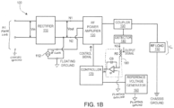
- FIG. 1A illustrates an example power converting system 100.
- the power converting system 100 includes a rectifier 110, a RF clock generator 112, a radio frequency (RF) power amplifier 120, a coupler 130, a detector 140, a RF load 150, a reference voltage generator 160, and the controller 170.
- the power converting system 100 may be implemented with an integrated circuit or with a combination of integrated circuits and/or individual discrete components.
- the power converting system 100 can be included in various electronic systems, including but not limited to: dryers, cooking appliances, industrial heaters, dialectic heaters, medical RF ablation systems, induction heaters, or radio transmitters.
- the rectifier 110 converts an input voltage (Vin) into an output voltage (Vout). Input of the rectifier 110 is coupled to an AC power line having a particular frequency, e.g., 60 Hz.
- the rectifier 110 can be a single-phase rectifier or a multi-phase rectifier, such as a three-phase rectifier.
- the rectifier 110 can be a full wave bridge rectifier. A full wave bridge rectifier provides excellent power efficiency.
- the rectifier 110 can be a Valley Fill rectifier. A Valley Fill rectifier improves power factor and power efficiency. In addition, a Valley Fill rectifier is cost-effective.
- elements of the rectifier 110 and elements following output of the rectifier 110 are coupled to floating ground rather than chassis ground.
- floating ground can be a common node that other voltages in the power converting system 100 are referenced to but is not tied to chassis or earth ground.
- the RF clock generator 112 During operation of the RF power amplifier 120, the RF clock generator 112 provides an RF clock to the RF power amplifier 120.
- the RF clock generator 112 is coupled to floating ground.
- An RF output frequency of the power converting system 100 is determined by the frequency of the RF clock.
- the RF power amplifier 120 is coupled to the output of the rectifier 110.
- the output of the rectifier 110 is coupled to an input of the RF power amplifier 120.
- the ground in the RF power amplifier 120 is isolated from chassis ground.
- One or more circuit elements requiring a connection to ground in the RF power amplifier 120 are coupled to floating ground.
- the RF power amplifier 120 is driven by the RF clock.
- the RF power amplifier 120 can be a class D, class DE, class E, or class F RF power amplifiers with various topologies. For example, a push pull and full bridge topology offer special advantages for RF power amplifiers requiring control of RF output power.
- the RF power amplifier 120 provides power to the RF load 150 through the coupler 130.
- the load voltage (V L ) across the RF load 150 can be the output voltage of the power converting system 100.
- the RF load 150 can include one or more resistances.
- RF power amplifier 120 includes a transformer. The RF load 150 is isolated from the input of the RF power amplifier 120. Thus, the RF load 150 is coupled to chassis ground.
- the coupler 130 also transfers the output of the RF power amplifier 120 to the detector 140.
- the coupler 130 can be a directional coupler. That is, the coupler 130 detects RF signals flowing in one direction, e.g., a direction from the RF power amplifier 120 to the RF load 150.
- the detector 140 is coupled to the output of the coupler 130.
- the detector 140 detects the output voltage of the RF power amplifier 120 and generates an output signal (OutputSignal).
- the detector 140 provides the output signal (OutputSignal) to the integrator 180.
- the integrator 180 converts the output signal (OutputSignal), which may be a complex waveform, to a DC voltage.
- the integrator 180 provides the converted DC voltage to the controller 170.
- the reference voltage generator 160 generates a reference voltage (Vref) and provides the reference voltage (Vref) to the controller 170.
- the reference voltage (Vref) represents the desired output power level of the power converting system 100.
- the controller 170 receives, as input, the DC voltage from the integrator 180 and the reference voltage (Vref) from the reference voltage generator 160.
- the controller 170 compares the DC voltage to the reference voltage (Vref). Based on the comparison of the DC voltage to the reference voltage (Vref), the controller 170 generates a control signal to control the RF power output of the power converting system 100.
- the controller 170 can calculate the difference between the DC voltage and the reference voltage (Vref).
- the controller 170 determines whether the difference satisfies a threshold, e.g., the difference is above the threshold or below the threshold. Based on a determination that the difference satisfies the threshold, the controller 170 can generate a control signal to control the RF power output of the power converting system 100.
- the control signal generated by the controller 170 adjusts one or more features of the RF power amplifier 120 to control the RF power output of the power converting system 100.
- the control signal generated by the controller 170 can adjust the phase of the RF clock within the RF power amplifier 120 to control the load voltage (V L ).
- the control signal generated by the controller 170 can adjust a pulse width of the RF clock within the RF power amplifier 120 to control the load voltage (V L ). By controlling the load voltage (V L ), the power converting system 100 can reduce power consumption of the power converting system 100.
- FIG. 1B illustrates another example power converting system 100.
- the integrator 180 includes a capacitor C0, a resistor R0, and an op amp OP.
- the resistor R0 is coupled between the node N3 and the node N4 and the capacitor C0 is coupled between the node N4 and the node N5.
- the node N3 is coupled to the output of detector 140
- the node N4 is coupled to a first inverting input terminal of the op amp OP.
- a second non-inverting input terminal of the op amp OP is coupled to floating ground.
- the integrator 180 converts the output signal (OutputSignal) from the detector 140 to a DC voltage.
- the converted DC voltage is provided to the controller 170.
- the operation of the controller 170 is the same as the controller 170 illustrated in FIG. 1A .
- FIG. 2A illustrates an example RF power amplifier 120 including a phase shifter 127.
- the phase shifter 127 can be an analog phase shifter. In some other implementations, the phase shifter 127 can be a digital phase shifter.
- the RF power amplifier 120 includes a first switching unit 121, a second switching unit 122, a third switching unit 123, a fourth switching unit 124, a transformer 125, a resonator 126, and a phase shifter 127.
- the switching units 121-124 can be implemented with a various kinds of transistors including, but not limited to: P-channel MOSFETs, N-channel MOSFETs, LDMOS transistors, Silicon MOSFETs, Silicon Carbide MOSFETs, Silicon Bipolar Transistors, Silicon IGBTs, Silicon JFETs, Silicon Carbide JFETs, Gallium Nitride High Electron Mobility Transistors (GaN HEMTs), GaAs MESFETs, or any suitable types of transistors.
- transistors including, but not limited to: P-channel MOSFETs, N-channel MOSFETs, LDMOS transistors, Silicon MOSFETs, Silicon Carbide MOSFETs, Silicon Bipolar Transistors, Silicon IGBTs, Silicon JFETs, Silicon Carbide JFETs, Gallium Nitride High Electron Mobility Transistors (GaN HEMTs), GaAs MESFETs, or any suitable types of transistors.
- the switching units 121-124 can be respectively driven by a suitable high current driver D1-D4 to charge or discharge input capacitance of the switching units 121-124.
- a suitable high current driver can charge the input capacitance within 5% of the RF signal's period.
- the high current driver can be controlled by transistor-transistor logic (TTL) or CMOS signals.
- TTL transistor-transistor logic
- CMOS complementary metal-oxide
- the switching units 121-124 are the same type of transistors.
- the switching units 121-124 are N-channel Silicon MOSFETs.
- the RF power amplifier 120 can include inverters for the second switching unit 122 and the fourth switching unit 124.
- the RF power amplifier 120 can include inverters for the first switching unit 121 and the third switching unit 123.
- the first switching unit 121 and the third switching unit 123 are the same type of transistors and the second switching unit 122 and the fourth switching unit 124 are the same type of transistors.
- the first switching unit 121 and the third switching unit 123 are N-channel Silicon MOSFETs and the second switching unit 122 and the fourth switching unit 124 are P-channel Silicon MOSFETs.
- the RF power amplifier 120 does not include inverters. The operations of the switching units 121-124 are described in greater detail below
- the first switching unit 121 is coupled between the node N1 and a node N9.
- the first switching unit 121 is turned on or off in response to the RF clock. For example, when the RF clock is high, the first switching unit 121 is turned on. When the RF clock is low, the first switching unit 121 is turned off.
- the RF power amplifier 120 additionally includes a driver D1 that is coupled between the node N10 and the first switching unit 121 to drive the first switching unit 121.
- the second switching unit 122 is coupled between the node N9 and the node N2.
- the second switching unit 122 is turned on or off in response to the RF clock. For example, when the RF clock is high, the second switching unit 122 is turned off. When the RF clock is low, the second switching unit 122 is turned on.
- the RF power amplifier 120 can include an inverter IN1 between the node N10 and the second switching unit 122.
- the first switching unit 121 and the second switching unit 122 are the same type of transistors.
- the second switching unit 122 can be a different type of transistor from the first switching unit 121.
- the RF power amplifier 120 does not include an inverter.
- the RF power amplifier 120 additionally includes a driver D2 between the node N10 and the second switching unit 122 to drive the second switching unit 122.
- the third switching unit 123 is coupled between the node N2 and a node N11.
- the third switching unit 123 is turned on or off in response to the RF clock. For example, where the phase of the RF clock is not shifted by the phase shifter 127, when the RF clock is high, the third switching unit 123 is turned on. When the RF clock is low, the third switching unit 123 is turned off. As another example, where the phase of the RF clock is shifted by the phase shifter 127, when the RF clock is high, the third switching unit 123 can be turned on or off based on how much the phase of the RF clock is shifted.
- the third switching unit 123 can be turned on or off based on how much the phase of the RF clock is shifted.
- the RF power amplifier 120 additionally includes a driver D3 that is coupled between the phase shifter 127 and the third switching unit 123 to drive the third switching unit 123.
- the fourth switching unit 124 is coupled between the node N11 and the node N1.
- the fourth switching unit 124 is turned on or off in response to the RF clock. For example, where the phase of the RF clock is not shifted by the phase shifter 127, when the RF clock is high, the fourth switching unit 124 is turned off. When the RF clock is low, the fourth switching unit 124 is turned on. As another example, where the phase of the RF clock is shifted by the phase shifter 127, when the RF clock is high, the fourth switching unit 124 can be turned on or off based on how much the phase of the RF clock is shifted.
- the fourth switching unit 124 can be turned on or off based on how much the phase of the RF clock is shifted.
- the RF power amplifier 120 can include an inverter IN2 between the phase shifter 127 and the fourth switching unit 124.
- the third switching unit 123 and the fourth switching unit 124 are the same type of transistors.
- the fourth switching unit 124 can be a different type of transistor from the third switching unit 123.
- the RF power amplifier 120 does not include an inverter.
- the RF power amplifier 120 additionally includes a driver D4 between the phase shifter 127 and the fourth switching unit 124 to drive the fourth switching unit 124.
- the transformer 125 is coupled between the node N9 and the node N11.
- the transformer 125 includes a primary and a secondary. Since the primary is separated from the secondary, the transformer 125 isolates the RF load 150 from the RF power amplifier 120 of the power converting system 100.
- the secondary of the transformer 125, the resonator 126, and the RF load 150 are coupled to chassis ground.
- the switching units 121-124 dissipate maximum power when the rectifier 110 delivers peak output voltage and the RF power output of the power converting system 100 is the maximum.
- the transformer 125 delivers RF power from the primary to the secondary.
- the secondary of the transformer 125 is coupled to the resonator 126.
- the resonator 126 is coupled to chassis ground.
- the power transferred from the primary to the secondary is transferred to the resonator 126 and the RF load 150.
- the resonator 126 has low impedance, e.g., less than 1 ohm. Thus, nearly all the power transferred from the primary to the secondary is transferred to the RF load 150.
- the phase shifter 127 couples the node N10 to both of the third switching unit 123 and the fourth switching unit 124. In response to the control signal received from the controller 170, the phase shifter 127 adjusts the phase of the RF clock and provides the phase-adjusted RF clock to both of the third switching unit 123 and the fourth switching unit 124 such that the output power of the RF power amplifier 120 is smoothly adjusted from zero to the maximum. Adjusting output power of the RF power amplifier 120 will be described in greater detail with reference to the FIG. 2C .
- FIG. 2B illustrates another example RF power amplifier 100 including a phase shifter 127.
- the switching units 121-124 are implemented using N-channel Silicon MOSFETs T1-T4.
- Each of the switching units 121-124 can additionally include any suitable circuit elements.
- the switching units 121-124 can be implemented using different types of transistors or other circuit elements.
- a drain of the transistor T1 is coupled to the node N1
- a gate of the transistor T1 is coupled to a node 12
- a source of the transistor T1 is coupled to the node N9.
- the transistor T1 is turned on or off.
- the transistor T1 is turned on.
- the transistor T1 is turned off.
- a drain of the transistor T2 is coupled to the node N9, a gate of the transistor T2 is coupled to a node 13, and a source of the transistor T2 is coupled to the node N2.
- the RF clock is inverted by the inverter IN1, driven by the driver D1, and then, provided to the gate of the transistor T2 to turn on or off the transistor T2.
- the transistor T2 is turned off.
- the transistor T2 is turned on.
- a drain of the transistor T3 is coupled to the node N11, a gate of the transistor T3 is coupled to a node N14, and a source of the transistor T3 is coupled to the node N2.
- the transistor T3 is turned on or off. When the RF clock is high, the transistor T3 is turned on. When the RF clock is low, the transistor T3 is turned off.
- a drain of the transistor T4 is coupled to the node N1, a gate of the transistor T4 is coupled to a node 15, and a source of the transistor T4 is coupled to the node N11.
- the RF clock is inverted by the inverter IN2, driven by the driver D4, and then, provided to the gate of the transistor T4 to turn on or off the transistor T4.
- the transistor T4 is turned off.
- the transistor T4 is turned on.
- the transformer 125 includes a primary L1 and a secondary L2 to deliver the voltage (V L1 ) between the node N9 and the node N11 into the load voltage (V L ).
- the transformer 125 includes two isolated coils L1, L2. These coils L1, L2 of the transformer 125 isolate the RF load 150 from the RF power amplifier 120 of the power converting system 100 as described above.
- the resonator 126 includes a resonant circuit including an inductor L1 and a capacitor C1. The RF load 150 is coupled to the resonator 126.
- the inductor L1 and the capacitor C1 have any suitable values of inductance and capacitance such that the resonant circuit of the resonator 126 has a resonant frequency that is the same as the operating frequency of the RF power amplifier 120 as determined by RF clock.
- the resonant frequency of the resonator 126 and the operating frequency of the RF power amplifier 120 can be 13.56 MHz.
- the resonator 126 has low impedance, e.g., less than 1 ohm, and nearly all the power from the secondary of the transformer is delivered to the RF load 150.
- the coupler 130 described with reference to FIGS. 1A and 1B can be coupled between the resonator 126 and the RF load 150.
- the phase shifter 127 is coupled between the node N10 and both of the node N14 and the node N15. In response to the control signal received from the controller 170, the phase shifter 127 adjusts the phase of the RF clock and provides the phase-adjusted RF clock to both of the gate of the transistor T3 and the gate of the transistor T4 such that the output power of the RF power amplifier 120 is smoothly adjusted from zero to the maximum.
- FIG. 2C illustrates an example timing chart showing voltage levels at the gates of the transistors T1-T4 and the voltage (V L1 ) in FIG. 2B .
- the node 12 is coupled to the gate of the transistor T1
- the node 13 is coupled to the gate of the transistor T2
- the node N14 is coupled to the gate of the transistor T3
- the node 15 is coupled to the gate of the transistor T4.
- the phase is not shifted, i.e., 0 degree phase shift
- the voltage (V L1 ) that is a voltage across the primary L1 of the transformer 125 is transitioned at the same timing that the RF clock is transitioned.
- the phase shifter 127 shifts the phase of the RF clock by 90 degrees, the voltages at the nodes N12, N13 are not shifted, but the voltages at the nodes N14, N15 are shifted by 90 degrees. As a result, the RMS voltage (V L1 ) is reduced comparing to the RMS voltage (V L1 ) with 0 degree phase shift.
- the phase shifter 127 shifts the phase of the RF clock by 180 degrees, the voltages at the nodes N12, N13 are not shifted, but the voltages at the nodes N14, N15 are shifted by 180 degrees. As a result, the voltage (V L1 ) has zero output.
- the RF power amplifier 120 can reduce the output, which is the voltage (V L1 ), of the RF power amplifier 120 such that the output of the RF power amplifier 120 is smoothly adjusted from zero to the maximum.
- the current flowing in the secondary L2 of the transformer 125 is filtered by the resonator 126, which can only pass the RF clock frequency.
- the load voltage (V L ) across the RF load 150 becomes a sign wave.
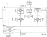
- FIG. 3A illustrates an example RF power amplifier, useful for understanding the invention but not covered by the scope of the invention, including a pulse width controller.
- the RF power amplifier 120 can include the same elements described with reference to FIG. 2A except the phase shifter 127. Instead of the phase shifter 127, the RF power amplifier 120 in FIG. 3A includes a pulse width controller 128.
- the pulse width controller 128 controls a pulse width of the RF clock.
- the pulse width controller 128 can be an analog pulse width controller.
- the pulse width controller 128 can be a digital pulse width controller.
- the pulse width controller 128 in FIG. 3A is coupled to all of the switching units 121-124.
- the pulse width controller 128 receives the RF clock as input and provides a pulse width-adjusted RF clock to the node N10.
- the pulse width controller 128 adjusts the pulse width of the RF clock and provides the pulse width-adjusted RF clock to all of the switching units 121-124 such that the output power of the RF power amplifier 120 is smoothly adjusted from zero to the maximum based on the adjustment of the pulse width.
- the power output adjustment achieved by adjusting the pulse width of the RF clock will be described in greater detail with reference to the FIG. 3C .
- FIG. 3B illustrates another example RF power amplifier, useful for understanding the invention but not covered by the scope of the invention, including a pulse width controller.
- the switching units 121-124 are implemented using N-channel Silicon MOSFETs T1-T4.
- Each of the switching units 121-124 can additionally include any suitable circuit elements.
- the switching units 121-124 can be implemented using different types of transistors or other circuit elements.
- the RF power amplifier 120 can include the same elements described with reference to FIG. 2B except the phase shifter 127. Instead of the phase shifter 127, the RF power amplifier 120 in FIG. 3B includes the pulse width controller 128. Where the phase shifter 127 in FIG. 2B is coupled to the gate of the transistor T3 and the gate of the transistor T4, but not coupled to the gate of the transistor T1 and the gate of the transistor T2, the pulse width controller 128 is respectively coupled to all of the gates of the transistors T1-T4. The pulse width controller 128 receives the RF clock as input and provides a pulse width-adjusted RF clock to the node N10.
- the pulse width controller 128 adjusts the pulse width of the RF clock and provides the pulse width-adjusted RF clock to all of the transistors T1-T4 such that the output power of the RF power amplifier 120 is smoothly adjusted from zero to the maximum.
- the output power adjustment achieved by the pulse width of the RF clock will be described in greater detail with reference to the FIG. 3C .
- FIG. 3C illustrates an example timing chart showing voltage levels at the gates of the transistors T1-T4 and the voltage (V L1 ) in FIG. 3B .
- the node 12 is coupled to the gate of the transistor T1
- the node 13 is coupled to the gate of the transistor T2
- the node N14 is coupled to the gate of the transistor T3
- the node 15 is coupled to the gate of the transistor T4.
- the pulse width controller 128 adjusts, i.e., reduces, the pulse width of the RF clock by 50%, the voltages at the nodes N12-N15 are respectively adjusted. As a result, the voltage (V L1 ) is reduced by 50% comparing to the voltage (V L1 ) when a pulse width of the RF clock is not adjusted.
- the pulse width controller 128 adjusts, i.e., reduces, the pulse width of the RF clock to zero, the voltage (V L1 ) has zero output.
- the RF power amplifier 120 can reduce the output of the RF power amplifier 120, which is the voltage (V L1 ), such that the output power of the RF power amplifier 120 is smoothly adjusted from zero to the maximum.
- FIG. 4A illustrates an example RF power amplifier including a phase shifter.
- the RF power amplifier 120 can include the same elements described with reference to FIG. 2A except that the RF power amplifier 120 includes two switching units, i.e., a fifth switching unit 221 and sixth switching unit 222 instead of the switching units 121-124.
- the switching units 221, 222 can be implemented with a various kinds of transistors including, but not limited to: P-channel MOSFETs, N-channel MOSFETs, LDMOS transistors, Silicon MOSFETs, Silicon Carbide MOSFETs, Silicon Bipolar Transistors, Silicon IGBTs, Silicon JFETs, Silicon Carbide JFETs, Gallium Nitride High Electron Mobility Transistors (GaN HEMTs), GaAs MESFETs, or any suitable types of transistors.
- the switching units 221, 222 are the same type of transistors.
- the switching units 221, 222 are N-channel Silicon MOSFETs.
- the RF power amplifier 120 can include an inverter for the fifth switching unit 221.
- the RF power amplifier 120 can include an inverter for the sixth switching unit 222.
- the fifth switching unit 221 is a different type of transistor from the sixth switching unit 222.
- the fifth switching unit 221 includes a P-channel Silicon MOSFET and the sixth switching unit 222 includes a N-channel Silicon MOSFET.
- the RF power amplifier 120 does not include inverters. The details of the switching units 221-222 are described in greater detail below.
- the fifth switching unit 221 is coupled between the node N9 and the node N2.
- the fifth switching unit 221 is turned on or off in response to the RF clock. For example, when the RF clock is high, the fifth switching unit 221 is turned off. When the RF clock is low, the fifth switching unit 221 is turned on.
- the RF power amplifier 120 can include an inverter IN3 between the node N10 and the fifth switching unit 221.
- the fifth switching unit 221 and the sixth switching unit 222 are the same type of transistors.
- the sixth switching unit 222 can be a different type of transistor from the fifth switching unit 221.
- the sixth switching unit 222 is a P-channel Silicon MOSFET.
- the RF power amplifier 120 does not include the inverter IN3.
- the RF power amplifier 120 additionally includes a driver D5 between the node N10 and the fifth switching unit 221 to drive the fifth switching unit 221.
- the sixth switching unit 222 is coupled between the node N2 and a node N11.
- the sixth switching unit 222 is turned on or off in response to the RF clock. For example, when the RF clock is high, the sixth switching unit 222 is turned on. When the RF clock is low, the sixth switching unit 222 is turned off.
- the RF power amplifier 120 additionally includes a driver D6 that is coupled between the phase shifter 127 and the sixth switching unit 222 to drive the sixth switching unit 222.
- the transformer 125 is coupled between the node N9 and the node N11.
- the transformer 125 includes a primary coupled between the node N9 and the node N11 and a secondary coupled to the resonator 126.
- the RF load 150 is coupled to the resonator 126.
- the node N1 is coupled to a portion of the transformer 125. In particular, the node N1 can be coupled to the center of the primary coil of the transformer 125.
- the transformer 125 delivers power from the primary to the secondary and the transferred power to the secondary is transferred to the resonator 126 and the RF load 150.
- the resonator 126 is coupled to chassis ground.
- the resonator 126 has low impedance, e.g., less than 1 ohm. Thus, nearly all the power transferred from the primary to the secondary is transferred to the RF load 150.
- the phase shifter 127 couples the node N10 to the sixth switching unit 222.
- the phase shifter 127 adjusts the phase of the RF clock and provides the phase-adjusted RF clock to both of the fifth switching unit 221 and the sixth switching unit 222 such that the output power of the RF power amplifier 120 is smoothly adjusted from zero to the maximum based on the adjustment of the phase.
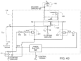
- FIG. 4B illustrates another example RF power amplifier including a phase shifter.
- the switching units 221, 222 are implemented using N-channel Silicon MOSFETs T5, T6.
- Each of the switching units 221, 222 can additionally include any suitable circuit elements.
- the switching units 221, 222 can be implemented using different types of transistors or other circuit elements.
- a drain of the transistor T5 is coupled to the node N9, a gate of the transistor T2 is coupled to the node 13, and a source of the transistor T2 is coupled to the node N2.
- the RF clock is inverted by the inverter IN3, driven by the driver D5, and then, provided to the gate of the transistor T5 to turn on or off the transistor T5. For example, when the RF clock is high, the transistor T5 is turned off. When the RF clock is low, the transistor T5 is turned on.
- a drain of the transistor T6 is coupled to the node N11, a gate of the transistor T6 is coupled to a node N14, and a source of the transistor T6 is coupled to the node N2.
- the transistor T6 is turned on or off. For example, where the phase of the RF clock is not shifted by the phase shifter 127, when the RF clock is high, the transistor T6 is turned on. When the RF clock is low, the transistor T6 is turned off. As another example, where the phase of the RF clock is shifted by the phase shifter 127, when the RF clock is high, the transistor T6 can be turned on or off based on how much the phase of the RF clock is shifted. When the RF clock is low, the transistor T6 can be turned on or off based on how much the phase of the RF clock is shifted.
- the transformer 125 includes a primary L1 and a secondary L2 to deliver the voltage (V L1 ) between the node N9 and the node N11 into the load voltage (V L ).
- the transformer 125 includes two isolated coils L1, L2. These coils L1, L2 of the transformer 125 isolate the RF load 150 from the RF power amplifier 120 of the power converting system 100 as described above.
- the resonator 126 includes a resonant circuit including an inductor L1 and a capacitor C1. The RF load 150 is coupled to the resonator 126.
- the inductor L1 and the capacitor C1 have any suitable values of inductance and capacitance such that the resonant circuit of the resonator 126 has a resonant frequency that is the same as the operating frequency of the RF power amplifier 120.
- the resonant frequency of the resonator 126 and the operating frequency of the RF power amplifier 120 can be 13.56 MHz.
- the resonator 126 has low impedance, e.g., less than 1 ohm, and nearly all the power from the secondary of the transformer is delivered to the RF load 150.
- the coupler 130 described with reference to FIGS. 1A and 1B can be coupled between the resonator 126 and the RF load 150.
- the phase shifter 127 is coupled between the node N10 and the node N14. In response to the control signal received from the controller 170, the phase shifter 127 adjusts the phase of the RF clock and provides the phase-adjusted RF clock to both of the gate of the transistor T5 and the gate of the transistor T6 such that the output power of the RF power amplifier 120 is smoothly adjusted from zero to maximum.
- FIG. 5A illustrates an example RF power amplifier, useful for understanding the invention but not covered by the scope of the invention, including a pulse width controller.
- the RF power amplifier 120 can include the same elements described with reference to FIG. 4A except the phase shifter 127. Instead of the phase shifter 127, the RF power amplifier 120 in FIG. 5A includes the pulse width controller 128.
- the pulse width controller 128 can be a pulse width controller described with reference to FIG. 3A .
- the pulse width controller 128 in FIG. 5A is coupled to both of the fifth switching unit 221 and the sixth switching unit 222.
- the pulse width controller 128 receives the RF clock as input and provides a pulse width-adjusted RF clock at the node N10.
- the pulse width controller 128 adjusts the pulse width of the RF clock and provides the pulse width-adjusted RF clock to all of the switching units 221, 222 such that the output power of the RF power amplifier 120 is smoothly adjusted from zero to maximum based on the adjustment of the pulse width.
- FIG. 5B illustrates another example RF power amplifier, useful for understanding the invention but not covered by the scope of the invention, including a pulse width controller.
- the switching units 221, 222 are implemented using N-channel Silicon MOSFETs T5, T6.
- Each of the switching units 221, 222 can additionally include any suitable circuit elements.
- the switching units 221, 222 can be implemented using different types of transistors or other circuit elements.
- the RF power amplifier 120 can include the same elements described with reference to FIG. 4B except the phase shifter 127. Instead of the phase shifter 127, the RF power amplifier 120 in FIG. 5B includes the pulse width controller 128.
- the pulse width controller 128 is respectively coupled to all of the gates of the transistors T5, T6.
- the pulse width controller 128 receives the RF clock as input and provides a pulse width-adjusted RF clock at the node N10.
- the pulse width controller 128 adjusts the pulse width of the RF clock and provides the pulse width-adjusted RF clock to all of the transistors T5, T6 such that the output of the RF power amplifier 120 is smoothly adjusted from zero to the maximum based on the adjustment of the pulse width.
Landscapes
- Engineering & Computer Science (AREA)
- Power Engineering (AREA)
- Amplifiers (AREA)
- Dc-Dc Converters (AREA)
Claims (8)
- Système de conversion de puissance (100) comportant :un redresseur (110) configuré pour convertir une tension d'entrée en une tension de sortie sur un premier noeud de sortie (N1) et incluant un second noeud de sortie (N2) qui est couplé à une masse flottante ;un amplificateur de puissance radiofréquence, RF, (120) couplé au premier noeud de sortie (N1) et au second noeud de sortie (N2) du redresseur (110) et configuré pour générer une tension de charge sur la base d'une horloge RF et de la tension de sortie ;un détecteur (140) couplé à l'amplificateur de puissance RF et configuré pour détecter la tension de charge de l'amplificateur de puissance RF ;un intégrateur (180) couplé au détecteur et configuré pour générer une tension continue, DC, basée sur la tension de charge détectée ;une commande (170) couplée à l'intégrateur et configurée pour, sur la base de la tension DC, générer un signal de commande pour régler une phase de l'horloge RF de l'amplificateur de puissance RF,un générateur d'horloge RF (112) couplé à l'amplificateur de puissance RF (120) et configuré pour fournir l'horloge RF à l'amplificateur de puissance RF (120),dans lequel l'amplificateur de puissance RF (120) inclut :un transformateur (125) incluant un côté primaire et un côté secondaire séparé du côté primaire et configuré pour transférer de la puissance RF du côté primaire au côté secondaire, le côté primaire du transformateur (125) étant couplé entre un premier noeud (N9) et un second noeud (N11), le premier noeud de sortie (N1) étant couplé à la fois au premier noeud (N9) et au second noeud (N11),un résonateur (126) couplé entre le côté secondaire du transformateur (125) et une charge RF (150),un déphaseur (127) configuré pour recevoir le signal de commande provenant de la commande (170) et, sur la base du signal de commande, régler la phase de l'horloge RF, etau moins deux unités de commutation incluant une deuxième unité de commutation (122, 221) qui est configurée pour recevoir un signal inversé de l'horloge RF et une troisième unité de commutation (123, 222) qui est configurée pour recevoir une horloge RF à phase réglée via le déphaseur (127),dans lequel la deuxième unité de commutation (122, 221) est couplée entre le premier noeud (N9) et le second noeud de sortie (N2) du redresseur (110) couplé à la masse flottante,dans lequel la troisième unité de commutation (123, 222) est couplée entre le second noeud (N11) et le second noeud de sortie (N2) du redresseur (110) couplé à la masse flottante,dans lequel le côté secondaire du transformateur (125), le résonateur (126) et la charge RF (150) sont couplés à la masse de châssis,dans lequel un premier noeud de sortie du générateur d'horloge RF (112) est couplé au déphaseur (127) et un noeud de masse du générateur d'horloge RF (112) est couplé au second noeud de sortie du redresseur (110), etdans lequel le noeud de masse du générateur d'horloge RF (112) est couplé à la masse flottante.
- Système de conversion de puissance (100) selon la revendication 1, comportant en outre : un générateur de tension de référence (160) configuré pour générer une tension de référence,
dans lequel la commande (170) est configurée pour : comparer la tension DC à la tension de référence, sur la base de la comparaison de la tension DC à la tension de référence, générer le signal de commande. - Système de conversion de puissance (100) selon la revendication 1, comportant en outre : un coupleur (130) ayant une entrée couplée à une sortie de l'amplificateur de puissance RF (120) et ayant une sortie couplée au détecteur (140).
- Système de conversion de puissance (100) selon la revendication 1, dans lequel l'amplificateur de puissance RF (120) inclut en outre :une première unité de commutation (121) qui est configurée pour recevoir l'horloge RF et qui est connectée entre le premier noeud de sortie (N1) du redresseur (110) et le premier noeud (N9), etune quatrième unité de commutation (124) qui est configurée pour recevoir un signal inversé de l'horloge RF via le déphaseur (127) et qui est connectée entre le premier noeud de sortie (N1) du redresseur (110) et le second noeud (N11),dans lequel le déphaseur (127) est configuré pour régler la phase de l'horloge RF et fournir l'horloge RF à phase réglée à la troisième unité de commutation (123) et à la quatrième unité de commutation (124).
- Système de conversion de puissance selon la revendication 4, dans lequel le résonateur (126) a une première fréquence de résonance, et
dans lequel une fréquence de fonctionnement de l'amplificateur de puissance RF (120) est égale à la première fréquence de résonance. - Système de conversion de puissance (100) selon la revendication 5, dans lequel la fréquence de fonctionnement de l'amplificateur de puissance RF (120) est comprise entre 100 kHz et 100 MHz.
- Système de conversion de puissance (100) selon la revendication 1, dans lequel une fréquence de fonctionnement de l'amplificateur de puissance RF (120) est comprise entre 13 et 43 MHz.
- Système de conversion de puissance (100) selon la revendication 1, dans lequel le premier noeud de sortie (N1) du redresseur (110) est couplé à un centre du côté primaire du transformateur (125).
Applications Claiming Priority (2)
| Application Number | Priority Date | Filing Date | Title |
|---|---|---|---|
| US201662493967P | 2016-07-21 | 2016-07-21 | |
| PCT/US2017/043413 WO2018018028A1 (fr) | 2016-07-21 | 2017-07-21 | Système de conversion de courant |
Publications (3)
| Publication Number | Publication Date |
|---|---|
| EP3488523A1 EP3488523A1 (fr) | 2019-05-29 |
| EP3488523A4 EP3488523A4 (fr) | 2020-03-11 |
| EP3488523B1 true EP3488523B1 (fr) | 2023-10-04 |
Family
ID=60990141
Family Applications (1)
| Application Number | Title | Priority Date | Filing Date |
|---|---|---|---|
| EP17832008.1A Active EP3488523B1 (fr) | 2016-07-21 | 2017-07-21 | Système de conversion de courant |
Country Status (6)
| Country | Link |
|---|---|
| US (1) | US10516371B2 (fr) |
| EP (1) | EP3488523B1 (fr) |
| KR (1) | KR102500530B1 (fr) |
| CN (1) | CN109792231B (fr) |
| AU (2) | AU2017300783A1 (fr) |
| WO (1) | WO2018018028A1 (fr) |
Citations (2)
| Publication number | Priority date | Publication date | Assignee | Title |
|---|---|---|---|---|
| JPH0583950A (ja) * | 1991-09-17 | 1993-04-02 | Toshiba Corp | 高周波電力変換装置 |
| US20020008981A1 (en) * | 2000-07-24 | 2002-01-24 | Chippower.Com, Inc. | High frequency sine wave AC Inverter |
Family Cites Families (21)
| Publication number | Priority date | Publication date | Assignee | Title |
|---|---|---|---|---|
| US5311143A (en) * | 1992-07-02 | 1994-05-10 | Motorola, Inc. | RF amplifier bias control method and apparatus |
| US6549071B1 (en) * | 2000-09-12 | 2003-04-15 | Silicon Laboratories, Inc. | Power amplifier circuitry and method using an inductance coupled to power amplifier switching devices |
| DE10161743B4 (de) * | 2001-12-15 | 2004-08-05 | Hüttinger Elektronik GmbH & Co. KG | Hochfrequenzanregungsanordnung |
| JP2006109687A (ja) * | 2004-06-02 | 2006-04-20 | Sony Corp | スイッチング電源回路 |
| US7151678B2 (en) * | 2004-12-15 | 2006-12-19 | Motorola, Inc. | Power system with redundant power supply apparatus |
| EP1701376B1 (fr) * | 2005-03-10 | 2006-11-08 | HÜTTINGER Elektronik GmbH + Co. KG | Generateur de plasma sous vide |
| TW200733523A (en) * | 2005-10-25 | 2007-09-01 | Koninkl Philips Electronics Nv | Power converter |
| JP4344751B2 (ja) * | 2007-01-19 | 2009-10-14 | 日立コンピュータ機器株式会社 | スイッチング電源 |
| CA2629235A1 (fr) * | 2007-04-17 | 2008-10-17 | Queen's University At Kingston | Convertisseur continu-continu avec reponse dynamique amelioree |
| US8817494B2 (en) * | 2010-08-09 | 2014-08-26 | Sanken Electric Co., Ltd. | PFC AC/DC converter reducing harmonics, switching loss, and switching noise |
| CN103078510B (zh) * | 2011-10-25 | 2015-11-25 | 通用电气公司 | 谐振电源、磁共振成像系统及控制方法 |
| WO2013082384A1 (fr) | 2011-12-01 | 2013-06-06 | Rf Micro Devices, Inc. | Convertisseur de puissance rf |
| US9306635B2 (en) * | 2012-01-26 | 2016-04-05 | Witricity Corporation | Wireless energy transfer with reduced fields |
| US9088247B2 (en) | 2013-02-15 | 2015-07-21 | St-Ericsson Sa | Method and apparatus for a multi-standard, multi-mode, dynamic, DC-DC converter for radio frequency power amplifiers |
| JP6367310B2 (ja) * | 2013-04-15 | 2018-08-01 | アジャンス スパシャル ユーロペエンヌ | 広帯域の包絡線追跡高周波パワー増幅器 |
| US20140361742A1 (en) * | 2013-06-07 | 2014-12-11 | Hong Kong Productivity Council | Electric vehicle charger |
| WO2015192133A2 (fr) * | 2014-06-13 | 2015-12-17 | University Of Maryland | Chargeur embarqué et intégré du type entre le réseau électrique et le véhicule (g2v) et entre le véhicule et le réseau électrique (v2g) et à double sortie pour des véhicules électriques enfichables |
| US10581274B2 (en) * | 2015-06-03 | 2020-03-03 | Lg Electronics Inc. | Home appliance |
| US10075055B2 (en) * | 2015-09-30 | 2018-09-11 | Apple Inc. | Zero-voltage-switching scheme for phase shift converters |
| US9814115B2 (en) * | 2015-12-25 | 2017-11-07 | Panasonic Intellectual Property Management Co., Ltd. | Illumination light communication apparatus and communication module |
| JP6707003B2 (ja) * | 2016-09-14 | 2020-06-10 | ローム株式会社 | スイッチ駆動回路及びこれを用いたスイッチング電源装置 |
-
2017
- 2017-07-21 AU AU2017300783A patent/AU2017300783A1/en not_active Abandoned
- 2017-07-21 US US15/657,075 patent/US10516371B2/en active Active
- 2017-07-21 KR KR1020197005185A patent/KR102500530B1/ko active IP Right Grant
- 2017-07-21 WO PCT/US2017/043413 patent/WO2018018028A1/fr unknown
- 2017-07-21 EP EP17832008.1A patent/EP3488523B1/fr active Active
- 2017-07-21 CN CN201780058184.9A patent/CN109792231B/zh active Active
-
2020
- 2020-10-02 AU AU2020244592A patent/AU2020244592B2/en active Active
Patent Citations (2)
| Publication number | Priority date | Publication date | Assignee | Title |
|---|---|---|---|---|
| JPH0583950A (ja) * | 1991-09-17 | 1993-04-02 | Toshiba Corp | 高周波電力変換装置 |
| US20020008981A1 (en) * | 2000-07-24 | 2002-01-24 | Chippower.Com, Inc. | High frequency sine wave AC Inverter |
Non-Patent Citations (1)
| Title |
|---|
| JAIN P ET AL: "A 20 KHZ HYBRID RESONANT POWER SOURCE FOR THE SPACE STATION", IEEE TRANSACTIONS ON AEROSPACE AND ELECTRONIC SYSTEMS, IEEE SERVICE CENTER, PISCATAWAY, NJ, US, vol. 25, no. 4, 1 July 1989 (1989-07-01), pages 491 - 496, XP000047591, ISSN: 0018-9251, DOI: 10.1109/7.32081 * |
Also Published As
| Publication number | Publication date |
|---|---|
| AU2020244592A1 (en) | 2020-11-05 |
| US20180026590A1 (en) | 2018-01-25 |
| WO2018018028A1 (fr) | 2018-01-25 |
| AU2017300783A1 (en) | 2019-03-07 |
| EP3488523A4 (fr) | 2020-03-11 |
| KR20190022907A (ko) | 2019-03-06 |
| CN109792231A (zh) | 2019-05-21 |
| CN109792231B (zh) | 2024-08-16 |
| KR102500530B1 (ko) | 2023-02-15 |
| EP3488523A1 (fr) | 2019-05-29 |
| US10516371B2 (en) | 2019-12-24 |
| AU2020244592B2 (en) | 2022-07-07 |
Similar Documents
| Publication | Publication Date | Title |
|---|---|---|
| TWI608690B (zh) | 操作於邊界導通模式之無橋式升壓功因修正轉換器所用之升壓電感器去磁化偵測 | |
| KR102193358B1 (ko) | 자기 발진 공진형 파워 컨버터 | |
| TWI406491B (zh) | 同步全橋整流電路及同步全波整流方法 | |
| JP7082203B2 (ja) | 整流回路およびこれを備えるデバイス | |
| EP3161948A1 (fr) | Circuit d'alimentation électrique incorporant des transformateurs pour la combinaison de sorties d'amplificateurs de puissance et l'isolation de circuits de calage de tension de charge | |
| JP2014113020A (ja) | 力率補正装置、電源装置及びモーター駆動装置 | |
| US10110071B2 (en) | Resonance-type power transmitter | |
| JP2005065497A (ja) | パルス幅変調ソフトスイッチング制御 | |
| US8593842B1 (en) | Method and apparatus for supplying and switching power | |
| US8704599B2 (en) | Switching power supply circuit | |
| WO2019012923A1 (fr) | Dispositif d'alimentation électrique haute fréquence | |
| EP3488523B1 (fr) | Système de conversion de courant | |
| US11539348B1 (en) | Open loop reactance matching circuitry | |
| US9923480B2 (en) | DC-to-AC power converter with high efficiency | |
| JP2021516031A (ja) | 電力コンバータ用フローティング接地絶縁型電源 | |
| KR102404053B1 (ko) | 스위치 구동회로 및 이를 포함하는 역률 보상 회로 | |
| EP2434644A1 (fr) | Topologie de commande de grille flottante haute tension pour fréquences de commutation très élevées | |
| JP2017099100A (ja) | スイッチング回路 | |
| JP6790324B2 (ja) | 高周波電源装置 | |
| US20220361299A1 (en) | Heating Circuit | |
| JP7021562B2 (ja) | 電力変換装置 | |
| JP2011205771A (ja) | ハーフブリッジ型コンバータ | |
| KR20150004301A (ko) | 역률 보정 장치, 전원 장치 및 모터 구동 장치 | |
| JP2017050989A (ja) | ワイヤレス電源供給装置及びこれを備えた高電圧素子駆動システム |
Legal Events
| Date | Code | Title | Description |
|---|---|---|---|
| STAA | Information on the status of an ep patent application or granted ep patent |
Free format text: STATUS: THE INTERNATIONAL PUBLICATION HAS BEEN MADE |
|
| PUAI | Public reference made under article 153(3) epc to a published international application that has entered the european phase |
Free format text: ORIGINAL CODE: 0009012 |
|
| STAA | Information on the status of an ep patent application or granted ep patent |
Free format text: STATUS: REQUEST FOR EXAMINATION WAS MADE |
|
| 17P | Request for examination filed |
Effective date: 20190220 |
|
| AK | Designated contracting states |
Kind code of ref document: A1 Designated state(s): AL AT BE BG CH CY CZ DE DK EE ES FI FR GB GR HR HU IE IS IT LI LT LU LV MC MK MT NL NO PL PT RO RS SE SI SK SM TR |
|
| AX | Request for extension of the european patent |
Extension state: BA ME |
|
| DAV | Request for validation of the european patent (deleted) | ||
| DAX | Request for extension of the european patent (deleted) | ||
| A4 | Supplementary search report drawn up and despatched |
Effective date: 20200207 |
|
| RIC1 | Information provided on ipc code assigned before grant |
Ipc: H01J 37/32 20060101ALI20200203BHEP Ipc: H02M 7/5387 20070101ALI20200203BHEP Ipc: H01S 3/097 20060101ALI20200203BHEP Ipc: H03F 1/02 20060101AFI20200203BHEP Ipc: H03F 3/193 20060101ALI20200203BHEP |
|
| STAA | Information on the status of an ep patent application or granted ep patent |
Free format text: STATUS: EXAMINATION IS IN PROGRESS |
|
| STAA | Information on the status of an ep patent application or granted ep patent |
Free format text: STATUS: EXAMINATION IS IN PROGRESS |
|
| 17Q | First examination report despatched |
Effective date: 20211004 |
|
| REG | Reference to a national code |
Ref country code: DE Ref legal event code: R079 Ref document number: 602017074978 Country of ref document: DE Free format text: PREVIOUS MAIN CLASS: H03F0001020000 Ipc: H03F0003190000 Ref country code: DE Ref legal event code: R079 Free format text: PREVIOUS MAIN CLASS: H03F0001020000 Ipc: H03F0003190000 |
|
| GRAP | Despatch of communication of intention to grant a patent |
Free format text: ORIGINAL CODE: EPIDOSNIGR1 |
|
| STAA | Information on the status of an ep patent application or granted ep patent |
Free format text: STATUS: GRANT OF PATENT IS INTENDED |
|
| RIC1 | Information provided on ipc code assigned before grant |
Ipc: H02M 7/04 20060101ALI20230421BHEP Ipc: H02M 7/06 20060101ALI20230421BHEP Ipc: H01J 37/32 20060101ALI20230421BHEP Ipc: H02M 7/5387 20070101ALI20230421BHEP Ipc: H03F 3/217 20060101ALI20230421BHEP Ipc: H03F 3/21 20060101ALI20230421BHEP Ipc: H03F 3/19 20060101AFI20230421BHEP |
|
| INTG | Intention to grant announced |
Effective date: 20230515 |
|
| RAP3 | Party data changed (applicant data changed or rights of an application transferred) |
Owner name: LG ELECTRONICS INC. |
|
| GRAS | Grant fee paid |
Free format text: ORIGINAL CODE: EPIDOSNIGR3 |
|
| GRAA | (expected) grant |
Free format text: ORIGINAL CODE: 0009210 |
|
| STAA | Information on the status of an ep patent application or granted ep patent |
Free format text: STATUS: THE PATENT HAS BEEN GRANTED |
|
| AK | Designated contracting states |
Kind code of ref document: B1 Designated state(s): AL AT BE BG CH CY CZ DE DK EE ES FI FR GB GR HR HU IE IS IT LI LT LU LV MC MK MT NL NO PL PT RO RS SE SI SK SM TR |
|
| REG | Reference to a national code |
Ref country code: GB Ref legal event code: FG4D |
|
| REG | Reference to a national code |
Ref country code: CH Ref legal event code: EP |
|
| REG | Reference to a national code |
Ref country code: IE Ref legal event code: FG4D |
|
| REG | Reference to a national code |
Ref country code: DE Ref legal event code: R096 Ref document number: 602017074978 Country of ref document: DE |
|
| REG | Reference to a national code |
Ref country code: LT Ref legal event code: MG9D |
|
| REG | Reference to a national code |
Ref country code: NL Ref legal event code: MP Effective date: 20231004 |
|
| REG | Reference to a national code |
Ref country code: AT Ref legal event code: MK05 Ref document number: 1618804 Country of ref document: AT Kind code of ref document: T Effective date: 20231004 |
|
| PG25 | Lapsed in a contracting state [announced via postgrant information from national office to epo] |
Ref country code: NL Free format text: LAPSE BECAUSE OF FAILURE TO SUBMIT A TRANSLATION OF THE DESCRIPTION OR TO PAY THE FEE WITHIN THE PRESCRIBED TIME-LIMIT Effective date: 20231004 |
|
| PG25 | Lapsed in a contracting state [announced via postgrant information from national office to epo] |
Ref country code: GR Free format text: LAPSE BECAUSE OF FAILURE TO SUBMIT A TRANSLATION OF THE DESCRIPTION OR TO PAY THE FEE WITHIN THE PRESCRIBED TIME-LIMIT Effective date: 20240105 |
|
| PG25 | Lapsed in a contracting state [announced via postgrant information from national office to epo] |
Ref country code: IS Free format text: LAPSE BECAUSE OF FAILURE TO SUBMIT A TRANSLATION OF THE DESCRIPTION OR TO PAY THE FEE WITHIN THE PRESCRIBED TIME-LIMIT Effective date: 20240204 |
|
| PG25 | Lapsed in a contracting state [announced via postgrant information from national office to epo] |
Ref country code: LT Free format text: LAPSE BECAUSE OF FAILURE TO SUBMIT A TRANSLATION OF THE DESCRIPTION OR TO PAY THE FEE WITHIN THE PRESCRIBED TIME-LIMIT Effective date: 20231004 |
|
| PG25 | Lapsed in a contracting state [announced via postgrant information from national office to epo] |
Ref country code: AT Free format text: LAPSE BECAUSE OF FAILURE TO SUBMIT A TRANSLATION OF THE DESCRIPTION OR TO PAY THE FEE WITHIN THE PRESCRIBED TIME-LIMIT Effective date: 20231004 |
|
| PG25 | Lapsed in a contracting state [announced via postgrant information from national office to epo] |
Ref country code: ES Free format text: LAPSE BECAUSE OF FAILURE TO SUBMIT A TRANSLATION OF THE DESCRIPTION OR TO PAY THE FEE WITHIN THE PRESCRIBED TIME-LIMIT Effective date: 20231004 |
|
| PG25 | Lapsed in a contracting state [announced via postgrant information from national office to epo] |
Ref country code: LT Free format text: LAPSE BECAUSE OF FAILURE TO SUBMIT A TRANSLATION OF THE DESCRIPTION OR TO PAY THE FEE WITHIN THE PRESCRIBED TIME-LIMIT Effective date: 20231004 Ref country code: IS Free format text: LAPSE BECAUSE OF FAILURE TO SUBMIT A TRANSLATION OF THE DESCRIPTION OR TO PAY THE FEE WITHIN THE PRESCRIBED TIME-LIMIT Effective date: 20240204 Ref country code: GR Free format text: LAPSE BECAUSE OF FAILURE TO SUBMIT A TRANSLATION OF THE DESCRIPTION OR TO PAY THE FEE WITHIN THE PRESCRIBED TIME-LIMIT Effective date: 20240105 Ref country code: ES Free format text: LAPSE BECAUSE OF FAILURE TO SUBMIT A TRANSLATION OF THE DESCRIPTION OR TO PAY THE FEE WITHIN THE PRESCRIBED TIME-LIMIT Effective date: 20231004 Ref country code: BG Free format text: LAPSE BECAUSE OF FAILURE TO SUBMIT A TRANSLATION OF THE DESCRIPTION OR TO PAY THE FEE WITHIN THE PRESCRIBED TIME-LIMIT Effective date: 20240104 Ref country code: AT Free format text: LAPSE BECAUSE OF FAILURE TO SUBMIT A TRANSLATION OF THE DESCRIPTION OR TO PAY THE FEE WITHIN THE PRESCRIBED TIME-LIMIT Effective date: 20231004 Ref country code: PT Free format text: LAPSE BECAUSE OF FAILURE TO SUBMIT A TRANSLATION OF THE DESCRIPTION OR TO PAY THE FEE WITHIN THE PRESCRIBED TIME-LIMIT Effective date: 20240205 |
|
| PG25 | Lapsed in a contracting state [announced via postgrant information from national office to epo] |
Ref country code: SE Free format text: LAPSE BECAUSE OF FAILURE TO SUBMIT A TRANSLATION OF THE DESCRIPTION OR TO PAY THE FEE WITHIN THE PRESCRIBED TIME-LIMIT Effective date: 20231004 Ref country code: RS Free format text: LAPSE BECAUSE OF FAILURE TO SUBMIT A TRANSLATION OF THE DESCRIPTION OR TO PAY THE FEE WITHIN THE PRESCRIBED TIME-LIMIT Effective date: 20231004 Ref country code: PL Free format text: LAPSE BECAUSE OF FAILURE TO SUBMIT A TRANSLATION OF THE DESCRIPTION OR TO PAY THE FEE WITHIN THE PRESCRIBED TIME-LIMIT Effective date: 20231004 Ref country code: NO Free format text: LAPSE BECAUSE OF FAILURE TO SUBMIT A TRANSLATION OF THE DESCRIPTION OR TO PAY THE FEE WITHIN THE PRESCRIBED TIME-LIMIT Effective date: 20240104 Ref country code: LV Free format text: LAPSE BECAUSE OF FAILURE TO SUBMIT A TRANSLATION OF THE DESCRIPTION OR TO PAY THE FEE WITHIN THE PRESCRIBED TIME-LIMIT Effective date: 20231004 Ref country code: HR Free format text: LAPSE BECAUSE OF FAILURE TO SUBMIT A TRANSLATION OF THE DESCRIPTION OR TO PAY THE FEE WITHIN THE PRESCRIBED TIME-LIMIT Effective date: 20231004 |
|
| REG | Reference to a national code |
Ref country code: DE Ref legal event code: R097 Ref document number: 602017074978 Country of ref document: DE |
|
| PG25 | Lapsed in a contracting state [announced via postgrant information from national office to epo] |
Ref country code: DK Free format text: LAPSE BECAUSE OF FAILURE TO SUBMIT A TRANSLATION OF THE DESCRIPTION OR TO PAY THE FEE WITHIN THE PRESCRIBED TIME-LIMIT Effective date: 20231004 |
|
| PG25 | Lapsed in a contracting state [announced via postgrant information from national office to epo] |
Ref country code: CZ Free format text: LAPSE BECAUSE OF FAILURE TO SUBMIT A TRANSLATION OF THE DESCRIPTION OR TO PAY THE FEE WITHIN THE PRESCRIBED TIME-LIMIT Effective date: 20231004 |
|
| PG25 | Lapsed in a contracting state [announced via postgrant information from national office to epo] |
Ref country code: SK Free format text: LAPSE BECAUSE OF FAILURE TO SUBMIT A TRANSLATION OF THE DESCRIPTION OR TO PAY THE FEE WITHIN THE PRESCRIBED TIME-LIMIT Effective date: 20231004 |
|
| PG25 | Lapsed in a contracting state [announced via postgrant information from national office to epo] |
Ref country code: SM Free format text: LAPSE BECAUSE OF FAILURE TO SUBMIT A TRANSLATION OF THE DESCRIPTION OR TO PAY THE FEE WITHIN THE PRESCRIBED TIME-LIMIT Effective date: 20231004 Ref country code: SK Free format text: LAPSE BECAUSE OF FAILURE TO SUBMIT A TRANSLATION OF THE DESCRIPTION OR TO PAY THE FEE WITHIN THE PRESCRIBED TIME-LIMIT Effective date: 20231004 Ref country code: RO Free format text: LAPSE BECAUSE OF FAILURE TO SUBMIT A TRANSLATION OF THE DESCRIPTION OR TO PAY THE FEE WITHIN THE PRESCRIBED TIME-LIMIT Effective date: 20231004 Ref country code: IT Free format text: LAPSE BECAUSE OF FAILURE TO SUBMIT A TRANSLATION OF THE DESCRIPTION OR TO PAY THE FEE WITHIN THE PRESCRIBED TIME-LIMIT Effective date: 20231004 Ref country code: EE Free format text: LAPSE BECAUSE OF FAILURE TO SUBMIT A TRANSLATION OF THE DESCRIPTION OR TO PAY THE FEE WITHIN THE PRESCRIBED TIME-LIMIT Effective date: 20231004 Ref country code: DK Free format text: LAPSE BECAUSE OF FAILURE TO SUBMIT A TRANSLATION OF THE DESCRIPTION OR TO PAY THE FEE WITHIN THE PRESCRIBED TIME-LIMIT Effective date: 20231004 Ref country code: CZ Free format text: LAPSE BECAUSE OF FAILURE TO SUBMIT A TRANSLATION OF THE DESCRIPTION OR TO PAY THE FEE WITHIN THE PRESCRIBED TIME-LIMIT Effective date: 20231004 |
|
| PLBE | No opposition filed within time limit |
Free format text: ORIGINAL CODE: 0009261 |
|
| STAA | Information on the status of an ep patent application or granted ep patent |
Free format text: STATUS: NO OPPOSITION FILED WITHIN TIME LIMIT |
|
| 26N | No opposition filed |
Effective date: 20240705 |