EP3464672B1 - Hochpräzises schattenmaskenabscheidungssystem und verfahren dafür - Google Patents
Hochpräzises schattenmaskenabscheidungssystem und verfahren dafür Download PDFInfo
- Publication number
- EP3464672B1 EP3464672B1 EP17802312.3A EP17802312A EP3464672B1 EP 3464672 B1 EP3464672 B1 EP 3464672B1 EP 17802312 A EP17802312 A EP 17802312A EP 3464672 B1 EP3464672 B1 EP 3464672B1
- Authority
- EP
- European Patent Office
- Prior art keywords
- substrate
- chuck
- shadow mask
- major surface
- mask
- Prior art date
- Legal status (The legal status is an assumption and is not a legal conclusion. Google has not performed a legal analysis and makes no representation as to the accuracy of the status listed.)
- Active
Links
Images





Classifications
-
- G—PHYSICS
- G03—PHOTOGRAPHY; CINEMATOGRAPHY; ANALOGOUS TECHNIQUES USING WAVES OTHER THAN OPTICAL WAVES; ELECTROGRAPHY; HOLOGRAPHY
- G03F—PHOTOMECHANICAL PRODUCTION OF TEXTURED OR PATTERNED SURFACES, e.g. FOR PRINTING, FOR PROCESSING OF SEMICONDUCTOR DEVICES; MATERIALS THEREFOR; ORIGINALS THEREFOR; APPARATUS SPECIALLY ADAPTED THEREFOR
- G03F7/00—Photomechanical, e.g. photolithographic, production of textured or patterned surfaces, e.g. printing surfaces; Materials therefor, e.g. comprising photoresists; Apparatus specially adapted therefor
- G03F7/70—Microphotolithographic exposure; Apparatus therefor
- G03F7/70691—Handling of masks or workpieces
- G03F7/707—Chucks, e.g. chucking or un-chucking operations or structural details
-
- C—CHEMISTRY; METALLURGY
- C23—COATING METALLIC MATERIAL; COATING MATERIAL WITH METALLIC MATERIAL; CHEMICAL SURFACE TREATMENT; DIFFUSION TREATMENT OF METALLIC MATERIAL; COATING BY VACUUM EVAPORATION, BY SPUTTERING, BY ION IMPLANTATION OR BY CHEMICAL VAPOUR DEPOSITION, IN GENERAL; INHIBITING CORROSION OF METALLIC MATERIAL OR INCRUSTATION IN GENERAL
- C23C—COATING METALLIC MATERIAL; COATING MATERIAL WITH METALLIC MATERIAL; SURFACE TREATMENT OF METALLIC MATERIAL BY DIFFUSION INTO THE SURFACE, BY CHEMICAL CONVERSION OR SUBSTITUTION; COATING BY VACUUM EVAPORATION, BY SPUTTERING, BY ION IMPLANTATION OR BY CHEMICAL VAPOUR DEPOSITION, IN GENERAL
- C23C14/00—Coating by vacuum evaporation, by sputtering or by ion implantation of the coating forming material
- C23C14/04—Coating on selected surface areas, e.g. using masks
- C23C14/042—Coating on selected surface areas, e.g. using masks using masks
-
- C—CHEMISTRY; METALLURGY
- C23—COATING METALLIC MATERIAL; COATING MATERIAL WITH METALLIC MATERIAL; CHEMICAL SURFACE TREATMENT; DIFFUSION TREATMENT OF METALLIC MATERIAL; COATING BY VACUUM EVAPORATION, BY SPUTTERING, BY ION IMPLANTATION OR BY CHEMICAL VAPOUR DEPOSITION, IN GENERAL; INHIBITING CORROSION OF METALLIC MATERIAL OR INCRUSTATION IN GENERAL
- C23C—COATING METALLIC MATERIAL; COATING MATERIAL WITH METALLIC MATERIAL; SURFACE TREATMENT OF METALLIC MATERIAL BY DIFFUSION INTO THE SURFACE, BY CHEMICAL CONVERSION OR SUBSTITUTION; COATING BY VACUUM EVAPORATION, BY SPUTTERING, BY ION IMPLANTATION OR BY CHEMICAL VAPOUR DEPOSITION, IN GENERAL
- C23C14/00—Coating by vacuum evaporation, by sputtering or by ion implantation of the coating forming material
- C23C14/06—Coating by vacuum evaporation, by sputtering or by ion implantation of the coating forming material characterised by the coating material
- C23C14/12—Organic material
-
- C—CHEMISTRY; METALLURGY
- C23—COATING METALLIC MATERIAL; COATING MATERIAL WITH METALLIC MATERIAL; CHEMICAL SURFACE TREATMENT; DIFFUSION TREATMENT OF METALLIC MATERIAL; COATING BY VACUUM EVAPORATION, BY SPUTTERING, BY ION IMPLANTATION OR BY CHEMICAL VAPOUR DEPOSITION, IN GENERAL; INHIBITING CORROSION OF METALLIC MATERIAL OR INCRUSTATION IN GENERAL
- C23C—COATING METALLIC MATERIAL; COATING MATERIAL WITH METALLIC MATERIAL; SURFACE TREATMENT OF METALLIC MATERIAL BY DIFFUSION INTO THE SURFACE, BY CHEMICAL CONVERSION OR SUBSTITUTION; COATING BY VACUUM EVAPORATION, BY SPUTTERING, BY ION IMPLANTATION OR BY CHEMICAL VAPOUR DEPOSITION, IN GENERAL
- C23C14/00—Coating by vacuum evaporation, by sputtering or by ion implantation of the coating forming material
- C23C14/22—Coating by vacuum evaporation, by sputtering or by ion implantation of the coating forming material characterised by the process of coating
- C23C14/24—Vacuum evaporation
-
- C—CHEMISTRY; METALLURGY
- C23—COATING METALLIC MATERIAL; COATING MATERIAL WITH METALLIC MATERIAL; CHEMICAL SURFACE TREATMENT; DIFFUSION TREATMENT OF METALLIC MATERIAL; COATING BY VACUUM EVAPORATION, BY SPUTTERING, BY ION IMPLANTATION OR BY CHEMICAL VAPOUR DEPOSITION, IN GENERAL; INHIBITING CORROSION OF METALLIC MATERIAL OR INCRUSTATION IN GENERAL
- C23C—COATING METALLIC MATERIAL; COATING MATERIAL WITH METALLIC MATERIAL; SURFACE TREATMENT OF METALLIC MATERIAL BY DIFFUSION INTO THE SURFACE, BY CHEMICAL CONVERSION OR SUBSTITUTION; COATING BY VACUUM EVAPORATION, BY SPUTTERING, BY ION IMPLANTATION OR BY CHEMICAL VAPOUR DEPOSITION, IN GENERAL
- C23C14/00—Coating by vacuum evaporation, by sputtering or by ion implantation of the coating forming material
- C23C14/22—Coating by vacuum evaporation, by sputtering or by ion implantation of the coating forming material characterised by the process of coating
- C23C14/24—Vacuum evaporation
- C23C14/28—Vacuum evaporation by wave energy or particle radiation
- C23C14/30—Vacuum evaporation by wave energy or particle radiation by electron bombardment
-
- C—CHEMISTRY; METALLURGY
- C23—COATING METALLIC MATERIAL; COATING MATERIAL WITH METALLIC MATERIAL; CHEMICAL SURFACE TREATMENT; DIFFUSION TREATMENT OF METALLIC MATERIAL; COATING BY VACUUM EVAPORATION, BY SPUTTERING, BY ION IMPLANTATION OR BY CHEMICAL VAPOUR DEPOSITION, IN GENERAL; INHIBITING CORROSION OF METALLIC MATERIAL OR INCRUSTATION IN GENERAL
- C23C—COATING METALLIC MATERIAL; COATING MATERIAL WITH METALLIC MATERIAL; SURFACE TREATMENT OF METALLIC MATERIAL BY DIFFUSION INTO THE SURFACE, BY CHEMICAL CONVERSION OR SUBSTITUTION; COATING BY VACUUM EVAPORATION, BY SPUTTERING, BY ION IMPLANTATION OR BY CHEMICAL VAPOUR DEPOSITION, IN GENERAL
- C23C14/00—Coating by vacuum evaporation, by sputtering or by ion implantation of the coating forming material
- C23C14/22—Coating by vacuum evaporation, by sputtering or by ion implantation of the coating forming material characterised by the process of coating
- C23C14/50—Substrate holders
-
- C—CHEMISTRY; METALLURGY
- C23—COATING METALLIC MATERIAL; COATING MATERIAL WITH METALLIC MATERIAL; CHEMICAL SURFACE TREATMENT; DIFFUSION TREATMENT OF METALLIC MATERIAL; COATING BY VACUUM EVAPORATION, BY SPUTTERING, BY ION IMPLANTATION OR BY CHEMICAL VAPOUR DEPOSITION, IN GENERAL; INHIBITING CORROSION OF METALLIC MATERIAL OR INCRUSTATION IN GENERAL
- C23C—COATING METALLIC MATERIAL; COATING MATERIAL WITH METALLIC MATERIAL; SURFACE TREATMENT OF METALLIC MATERIAL BY DIFFUSION INTO THE SURFACE, BY CHEMICAL CONVERSION OR SUBSTITUTION; COATING BY VACUUM EVAPORATION, BY SPUTTERING, BY ION IMPLANTATION OR BY CHEMICAL VAPOUR DEPOSITION, IN GENERAL
- C23C14/00—Coating by vacuum evaporation, by sputtering or by ion implantation of the coating forming material
- C23C14/22—Coating by vacuum evaporation, by sputtering or by ion implantation of the coating forming material characterised by the process of coating
- C23C14/54—Controlling or regulating the coating process
-
- H—ELECTRICITY
- H10—SEMICONDUCTOR DEVICES; ELECTRIC SOLID-STATE DEVICES NOT OTHERWISE PROVIDED FOR
- H10K—ORGANIC ELECTRIC SOLID-STATE DEVICES
- H10K71/00—Manufacture or treatment specially adapted for the organic devices covered by this subclass
- H10K71/10—Deposition of organic active material
- H10K71/16—Deposition of organic active material using physical vapour deposition [PVD], e.g. vacuum deposition or sputtering
- H10K71/166—Deposition of organic active material using physical vapour deposition [PVD], e.g. vacuum deposition or sputtering using selective deposition, e.g. using a mask
-
- H—ELECTRICITY
- H10—SEMICONDUCTOR DEVICES; ELECTRIC SOLID-STATE DEVICES NOT OTHERWISE PROVIDED FOR
- H10P—GENERIC PROCESSES OR APPARATUS FOR THE MANUFACTURE OR TREATMENT OF DEVICES COVERED BY CLASS H10
- H10P72/00—Handling or holding of wafers, substrates or devices during manufacture or treatment thereof
- H10P72/50—Handling or holding of wafers, substrates or devices during manufacture or treatment thereof for positioning, orientation or alignment
- H10P72/57—Mask-wafer alignment
-
- H—ELECTRICITY
- H10—SEMICONDUCTOR DEVICES; ELECTRIC SOLID-STATE DEVICES NOT OTHERWISE PROVIDED FOR
- H10P—GENERIC PROCESSES OR APPARATUS FOR THE MANUFACTURE OR TREATMENT OF DEVICES COVERED BY CLASS H10
- H10P72/00—Handling or holding of wafers, substrates or devices during manufacture or treatment thereof
- H10P72/70—Handling or holding of wafers, substrates or devices during manufacture or treatment thereof for supporting or gripping
- H10P72/72—Handling or holding of wafers, substrates or devices during manufacture or treatment thereof for supporting or gripping using electrostatic chucks
Definitions
- the present invention relates to thin-film deposition in general, and, more particularly, evaporation-based thin-film deposition. It is yet another aspect of the present invention that a mask chuck can include features that mitigate gravity-induced sag of a shadow mask
- Shadow-mask-based deposition is a process by which a layer of material is deposited onto the surface of a substrate such that the desired pattern of the layer is defined during the deposition process itself. This is deposition technique is sometimes referred to as "direct patterning.”
- the desired material is vaporized at a source that is located at a distance from the substrate, with a shadow mask positioned between them.
- the vaporized atoms of the material travel toward the substrate, they pass through a set of through-holes in the shadow mask, which is positioned just in front of the substrate surface.
- the through-holes i.e., apertures
- the shadow mask blocks passage of all vaporized atoms except those that pass through the through-holes, which deposit on the substrate surface in the desired pattern.
- Shadow-mask-based deposition is analogous to silk-screening techniques used to form patterns ( e . g ., uniform numbers, etc.) on articles of clothing or stenciling used to develop artwork.
- Shadow-mask-based deposition has been used for many years in the integrated-circuit (IC) industry to deposit patterns of material on substrates, due, in part, to the fact that it avoids the need for patterning a material layer after it has been deposited. As a result, its use eliminates the need to expose the deposited material to harsh chemicals (e.g., acid-based etchants, caustic photolithography development chemicals, etc .) to pattern it. In addition, shadow-mask-based deposition requires less handling and processing of the substrate, thereby reducing the risk of substrate breakage and increasing fabrication yield. Furthermore, many materials, such as organic materials, cannot be subjected to photolithographic chemicals without damaging them, which makes depositing such materials by shadow mask a necessity.
- harsh chemicals e.g., acid-based etchants, caustic photolithography development chemicals, etc .
- a shadow mask must be supported only at its perimeter to avoid blocking the passage of the vaporized atoms to the through-hole pattern. As a result, the center of the shadow mask can sag due to gravity, which further exacerbates feathering issues.
- each pixel of an active-matrix organic light-emitting-diode (AMOLED) display normally includes several regions of organic light-emitting material, each of which emits a different color of light.
- AMOLED displays Due to feathering issues, prior-art AMOLED displays have typically been restricted to approximately 600 pixels-per-inch (ppi) or less, which is insufficient for many applications, such as near-to-eye augmented reality and virtual-reality applications.
- ppi pixels-per-inch
- the need for large gaps within and between the pixels gives rise to a reduced pixel fill factor, which reduces display brightness.
- the current density through the organic layers must be increased to provide the desired brightness, which can negatively impact display lifetime.
- An alternative approach is to use a shadow-mask with an aperture as large as the active area of the display itself to deposit a monochrome white-emitting organic layer across the entire display and then to pattern or deposit red, green and blue color filters on top of the OLED.
- These color filters absorb all of the emitted white light except for the red, green or blue portion of the spectrum (depending on the color filter), allowing a full color image to be created.
- these color filters absorb up to 80% of the emitted light which significantly reduces display brightness, again requiring operation at higher than desirable drive currents.
- Embodiments of the present invention enables high-resolution direct deposition of a patterned layer of material on a substrate without some of the costs and disadvantages of the prior art.
- Embodiments of the present invention filter the propagation angles of vaporized atoms to a narrow range around a direction normal to the surface of the substrate. As a result, feathering of deposited material outside the lateral dimensions of features of a shadow mask is mitigated.
- Embodiments of the present invention are particularly well suited for use in deposition of sensitive materials, such as organic light-emitting material.
- Embodiments are also well suited for deposition of other thin- and thick-film layers in packaging applications, integrated-circuit processing applications, and the like.
- the present invention further enables high-precision alignment of a shadow mask and substrate that can be in contact or separated by only a few microns.
- Embodiments of the present invention are particularly well suited for applications requiring high-density patterns of material on a substrate, such as dense-pixel displays (DPD), high-definition displays, and the like.
- DPD dense-pixel displays
- An illustrative embodiment of the present invention is a direct-patterning deposition system in which a material is vaporized at a source such that it deposits on a surface of a substrate after passing through an aperture pattern of a shadow mask. Prior to their arrival at the shadow mask, the vaporized atoms pass through a collimator that blocks all vaporized atoms except those having propagation angles close to the direction normal to the substrate surface. As a result, the lateral deviation between the apertures and their respective regions of deposited material is reduced as compared to the prior art.
- the collimator includes a plurality of channels having a high height-to-width aspect ratio, where the longitudinal axis of the channels is substantially aligned with the normal direction. As a result, those vaporized atoms travelling along directions other than close to normal are blocked by the inside walls of the channels.
- the source is dimensioned and arranged to provide a conically shaped vapor plume of vaporized atoms such that the entire substrate surface receives vaporized material at the same time. In some of these embodiments, the source is moved along a path such that the uniformity of the thickness of deposited material is improved over the two-dimensional area of the substrate surface.
- the source is a linear source that emits a fan-shaped vapor plume, where the linear source is moved along a direction that is unaligned with its longitudinal axis. In some of these embodiments, the source is moved along a direction that is substantially orthogonal to both the longitudinal axis of the source and the normal direction. In some of these embodiments, the source is moved along a non-linear path.
- the source includes a plurality of individual nozzles, each of which emits a conically shaped vapor plume such that the nozzles collectively provide a flow of vaporized atoms that is substantially uniform over the area of the substrate surface.
- the source is a two-dimensional planar source that is arranged parallel to and facing the substrate such that, when heated, organic material vaporizes uniformly across the planar surface of the source.
- relative motion between the source and shadow mask is provided to improve the thickness uniformity of the deposited material over the two-dimensional area of the substrate surface.
- Another illustrative embodiment of the present invention is a direct-patterning deposition system comprising a first chuck having a first mounting surface for holding a substrate and a second chuck having a second mounting surface for holding a shadow mask that comprises a pattern of through-holes.
- the second chuck includes (1) a frame that surrounds a central opening that exposes the pattern of though-holes in the shadow mask and (2) a grid for supporting the shadow mask, where the grid and frame are mechanically attached via a plate.
- the first chuck generates a first electrostatic force that is selectively applied to the back surface of the substrate.
- the first chuck is also dimensioned and arranged such that it does not project above the front surface of the substrate.
- the second chuck generates a second electrostatic force that is selectively applied to the back surface of the shadow mask.
- the second chuck is also dimensioned and arranged so that it does not project above the front surface of the shadow mask.
- At least one of the first and second attractive forces is a force other than electrostatic, such as a vacuum-generated force, a magnetic force, etc.
- the second mounting surface is dimensioned and arranged to create a tensile stress in the front surface of the shadow mask that mitigates gravity-induced sag of its central region.
- the frame of the second chuck is shaped such that its mounting surface slopes away from top edge of the inner perimeter of the frame. As a result, when the shadow mask is mounted in the second chuck, the shadow mask becomes slightly bowed, which induces a tensile stress in the front surface of the shadow mask.
- the mounting surface is curved downward from the top edge of the inner perimeter of the frame.
- ribs which can support a central membrane portion of a shadow mask, thereby keeping it flat and mitigating the effect of gravity
- FIG. 1 depicts a schematic drawing of a cross-section of the salient features of a direct-patterning deposition system in accordance with the prior art.
- System 100 is a conventional evaporation system that deposits a desired pattern of material on a substrate by evaporating the material through a shadow mask positioned in front of the substrate.
- System 100 includes source 104 and shadow mask 106, which are arranged within a low-pressure vacuum chamber (not shown).
- Substrate 102 is a glass substrate suitable for the formation of active-matrix organic-light-emitting-diode (AMOLED) displays.
- Substrate 102 includes surface 114, which defines plane 108 and normal axis 110. Normal axis 110 is orthogonal to plane 108.
- Surface 114 includes a plurality of deposition sites, G, for receiving material that emits green light, a plurality of deposition sites, B, for receiving material that emits blue light, and a plurality of deposition sites, R, for receiving material that emits red light.
- the deposition sites are arranged in a plurality of pixel regions 112 such that each pixel region includes one deposition site for the light-emitting material of each color.
- Source 104 is a crucible for vaporizing material 116, which is an organic material that emits light at a desired wavelength.
- material 116 is an organic light-emitting material that emits red light.
- source 104 is a single-chamber crucible that is centered with respect to substrate 102; however, in some embodiments, source 104 includes a plurality of chambers that are arranged in one- and/or two-dimensional arrangements.
- Shadow mask 106 is a plate of structural material that includes apertures 120. Shadow mask is substantially flat and defines plane 118. The shadow mask is located between source 104 and substrate 102 such that it blocks the passage of all of the vaporized atoms except those that pass through its apertures. The shadow mask and substrate are separated by separation, s, (typically a few tens or hundreds of microns), planes 108 and 118 are substantially parallel, and apertures 120 are aligned with deposition sites R.
- vaporized atoms are incident only on deposition sites R.
- vapor plume 124 includes vaporized atoms that travel along many different propagation directions 126, many of which are not aligned with the direction of normal axis 110.
- a large fraction of the vaporized atoms that pass through apertures 120 are travelling along propagation directions that have a significant lateral component.
- the point at which each vaporized atom is incident on surface 114 is geometrically determined by its propagation angle and the spatial relationship between the substrate and shadow mask - specifically, spacing s and the alignment of apertures 120 with deposition sites R.
- propagation angle is defined as the angle formed by the propagation direction of a vaporized atom with respect to the direction normal to plane 108 of substrate 102 (i.e., normal direction 128, which is aligned with normal axis 110).
- vaporized atom 122 travels along a propagation direction 126, which forms propagation angle, ⁇ p, with respect to normal direction 128.
- the propagation angles of the vaporized atoms of vapor plume 124 span a relatively large angular range of - ⁇ m to + ⁇ m , which gives rise to significant disadvantages for prior-art direct-deposition systems.
- it results in the deposition of material 118 on front surface 114 outside the perimeter of apertures 120, which is typically referred to as "feathering.”
- the amount of feathering at an aperture increases with the distance of that aperture from the center of substrate 102.
- vaporized atoms 122 arriving at shadow mask 106 have propagation angles that are within a relatively small angular range. In other words, they are travelling along directions that are only slightly misaligned with normal axis 110. As a result, vaporized atoms that pass through these apertures exhibit only minimal lateral drift (i.e., feathering) after passing through the shadow mask. In this region, therefore, the lateral extent of the deposited material 116 is typically nearly aligned with the edges of apertures 120 ( i.e., it deposits primarily on the targeted deposition sites R ).
- vaporized atoms arriving at shadow mask 106 span a relatively larger angular range and include propagation angles closer to
- the lateral distance traveled by vaporized atoms after passing through the shadow mask is greater, leading to deposited material feathering out well beyond the lateral extent of the aperture.
- ⁇ f a lateral offset between the edges of the aperture openings and the perimeters of the areas in which material 116 deposits.
- the deposited material therefore, extends beyond the area of the targeted deposition sites.
- such feathering can lead to deposition of material on adjacent deposition sites that are intended for different light-emitting material ( i . e ., deposition sites, B and/or G ), thereby leading to color mixing.
- feathering is exacerbated by any additional misalignments between the shadow mask and substrate, such as deviations from the parallelism of planes 108 and 118 ( i . e ., relative pitch and/or yaw between the mask and substrate), non-flatness of the shadow mask and/or substrate, and translational and/or rotational misalignment between the shadow mask and substrate. Still further, in many prior-art deposition systems ( e . g ., systems for depositing more than one material, etc .), source 104 is located off-center from the substrate, which leads to even greater feathering problems.
- prior-art substrate and shadow mask chucks typically include features that project above the substrate and shadow mask, respectively. As a result, these features act as blocking elements that limit how closely the substrate and shadow mask can be positioned.
- contact with the shadow mask can cause damage to existent structures on the surface of the substrate.
- damage to the shadow mask can result from contact with the substrate.
- residue can be left on the shadow mask surface upon removal from contact with the substrate. Frequent cleaning of the shadow mask then becomes necessary, which increases process time and overall cost, while also creating the potential for mask damage during the cleaning operations.
- prior-art shadow mask deposition has been substantially limited to non-contact configurations in which feathering has significant negative impact.
- conventional shadow masks are normally made of metal and are, therefore, necessarily quite thick. When placed in contact with the substrate, a thick shadow mask gives rise to shadowing within each aperture region that results in the edges of the deposited features being thinner. For thicker shadow masks, such as those typically used in the prior art, more material is lost due to the walls of the apertures and the edges of the sub-pixel become thinner.
- the present invention enables direct deposition without some of the disadvantages of the prior art, however. It is a first aspect of the present invention that feathering can be significantly reduced by allowing only vaporized atoms that propagate along directions nearly normal to the surface of the substrate to reach the shadow mask, thereby enabling patterns of deposited material having higher resolution and fidelity to the aperture pattern of the shadow mask.
- a non-metal material such as silicon nitride
- a shadow mask enables it to be extremely thin ( ⁇ 1 micron), thereby giving rise to significantly less shadowing that prior-art shadow masks.
- substrate and shadow-mask chucks having no structure that projects above the top surface of the substrate and shadow mask enables extremely small separation, or even contact, between the substrate and shadow mask, thereby mitigating feathering.
- Substrate/shadow mask contact can also increase their stability during deposition, improve material utilization by reducing waste, enable faster deposition and higher throughput, and enable deposition at lower temperatures.
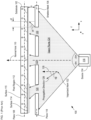
- FIG. 2 depicts a schematic drawing of a cross-section of the salient features of a high-precision, direct-patterning deposition system in accordance with an illustrative embodiment of the present invention.
- System 200 includes vacuum chamber 202, substrate chuck 204, source 104, shadow mask 106, mask chuck 206, collimator 208, and positioning system 212.
- System 200 is operative for evaporating a desired pattern of material onto a substrate surface without the need for subsequent subtractive patterning operations, such as photolithography and etching.
- System 200 is described herein with respect to the deposition of a pattern of light-emitting material on a glass substrate as part of the fabrication of an AMOLED display.
- the present invention can be directed toward the formation of directly patterned layers of virtually any thin- and thick-film material (organic or inorganic) on any of a wide range of substrates, such as semiconductor substrates (e.g., silicon, silicon carbide, germanium, etc. ), ceramic substrates, metal substrates, plastic substrates, and the like.
- the illustrative embodiment is a thermal evaporation system
- the present invention can be directed toward virtually any material-deposition process, such as e-beam evaporation, sputtering, and the like.
- the depicted example is a deposition system suitable for use in single-substrate planar processing
- the present invention is also suitable for use in other fabrication approaches, such as cluster-tool processing, track processing, roll-to-roll processing, reel-to-reel processing, etc.
- the present invention is suitable for use in myriad applications including, without limitation, packaging applications, IC fabrication, MEMS fabrication, nanotechnology device fabrication, ball-grid array (BGA) fabrication, and the like.
- BGA ball-grid array
- shadow mask 106 is a high-precision shadow mask comprising handle substrate 224 and membrane 226, which is suspended over a central opening formed in the handle substrate.
- Membrane 226 includes through-hole pattern 228.
- Shadow mask 106 includes two major surfaces - front surface 230 and back surface 232.
- Front surface 230 is the top surface of membrane 226 (i.e., the membrane surface distal to handle substrate 224), which defines plane 118.
- Back surface 232 is the surface of handle substrate 224 (i.e., the substrate surface distal to membrane 226).
- membrane 226 comprises silicon nitride; however, other materials can be used without departing from the scope of the present invention.
- membrane 226 has a thickness that is less than or equal to one micron; however, other thicknesses can be used for the membrane without departing from the scope of the present invention.
- a shadow-mask membrane having a thickness of one micron or less can reduce shadowing effects during direct deposition as compared to prior-art shadow masks.
- Vacuum chamber 202 is a conventional pressure vessel for containing a low-pressure environment required for the evaporation of material 116.
- vacuum chamber 110 is a standalone unit; however, it can also be realized as a part of a cluster deposition system or track-deposition system where multiple evaporation chambers are arranged in linear chain without departing from the scope of the present invention.
- vacuum chamber 110 includes several evaporation sources/shadow mask combinations that enable formation of different patterns of different materials on substrate 102, such as, for example, multiple light-emitting subpixels that emit light at different colors (e.g., red, green, and blue).
- Controller 240 is a conventional instrument controller that, among other things, provides control signals 236 and 238 to substrate chuck 204 and mask chuck 206, respectively.
- FIG. 3 depicts operations of a method for depositing a directly patterned layer of material on a substrate in accordance with the illustrative embodiment.
- Method 300 is described herein with continuing reference to FIG. 2 , as well as reference to FIGS. 4A-B, 5, 6A-B, 7A-B, 8A-B, 9, 10 and 11A-C.
- Method 300 begins with operation 301, wherein collimator 208 is mounted in collimator chuck 210.
- Collimator 208 is a mechanically robust plate comprising a plurality of channels that are separated by thin walls, as described in more detail below and with respect to FIGS. 11A-C .
- Collimator 208 is dimensioned and arranged to function as a spatial filter that selectively passes vaporized atoms propagating along directions that are nearly normal to plane 108 ( i.e., that have very small propagation angles). Collimator 202, therefore, mitigates feathering across the entirety of substrate 102.
- Collimator chuck 210 is an annular clamping mechanism for holding and locating the collimator relative to shadow mask 106.
- shadow mask 106 is mounted in mask chuck 206.
- Mask chuck 206 is a fixture for holding shadow mask 106 via an attractive force imparted on only its back surface.
- mask chuck 206 holds shadow mask 106 using electrostatic force.
- mask chuck 206 holds a shadow mask via a different attractive force, such as a vacuum-generated force, a magnetic force, etc.
- mask chuck 206 is a mechanical clamp.
- FIGS. 4A-B depicts a schematic drawings of top and cross-section views, respectively, of a mask chuck in accordance with the illustrative embodiment.
- the cross-section depicted in FIG. 4B is taken through line a-a shown in FIG. 4A .
- Mask chuck 206 includes frame 402, electrodes 404-1 and 404-2, and pads 406.
- Frame 402 is a structurally rigid circular ring of electrically insulating material. Frame 402 surrounds opening 408, which is sufficiently large to expose the entirety of through-hole pattern 228. In some embodiments, frame 402 has a shape other than circular, such as square, rectangular, irregular, etc. In some embodiments, frame 402 comprises an electrically conductive material that is coated with an electrical insulator.
- Electrodes 404-1 and 404-2 are electrically conductive elements formed on the surface of frame 402. Electrodes 404-1 and 404-2 are electrically coupled with controller 240.
- Pads 406 are structurally rigid plates of electrically insulating material disposed on electrodes 404-1 and 404-2. Each of pads 406 includes mounting surface 410, against which shadow mask 106 is held when mounted in the mask chuck.
- FIG. 5 depicts a cross-sectional view of shadow mask 106 mounted in mask chuck 206.
- Shadow mask 106 is held in mask chuck 206 by an electrostatic force imparted between mounting surface 410 and back surface 232.
- the electrostatic force arises in response to a voltage potential between electrodes 404-1 and 404-2, which is generated by control signal 238.
- back surface 232 is brought into contact with mounting surface 410, sympathetic charge regions develop within handle substrate 224 as shown. As a result, the electrostatic force is selectively imparted between back surface 232 and mounting surface 410.
- mask chucks in accordance with the present invention include one or more features that mitigate or eliminate gravity-induced sag of a shadow mask when the shadow mask is mounted.
- a shadow mask can sag by several microns in the center due to its own mass and the effect of gravity. This gravity-induced sag leads to several significant issues that exacerbate feathering.
- it increases the separation between the shadow mask and the substrate in the center of the deposition region, which is typically centered on the shadow mask. As discussed above, feathering increases with substrate/shadow mask separation distance.
- a mask chuck can include features that mitigate gravity-induced sag of a shadow mask.
- mask chuck 206 includes a slight curvature (e.g., an upward slope) that biases the shadow mask upward to counteract shadow-mask sag due to gravity.
- a fine support structure may extend across the opening in mask chuck 206 to support the mask and reduce the gravitational sag.
- FIG. 6A-B depicts a schematic drawing of a cross-sectional view of a portion of a mask chuck in accordance with a first alternative embodiment but which is not covered by the present invention.
- the cross-section depicted in FIG. 6A is taken through line a-a shown in FIG. 4A .
- Mask chuck 600 includes frame 402, electrodes 404-1 and 404-2, and pads 702.
- Pads 602 are analogous to pads 406 described above; however, each pad 602 has a mounting surface that is designed to induce or increase tensile strain in the shadow-mask when it is mounted in the mask chuck.
- Pad 602 has mounting surface 604, which is linearly tapered downward from inner edge 606 ( i.e., the edge proximal to opening 408) to outer edge 608.
- mounting surface 604 tapers in the negative z-direction, as shown, from point 614 to point 616 ( i.e., where from it meets inner edge 606 at plane 610 to where it meets outer edge 608 at plane 612).
- inner edge 606 and mounting surface 604 form interior angle, ⁇ , such that it is an acute angle.
- shadow mask 106 When shadow mask 106 is held in mask chuck 600, back surface 232 is attracted to mounting surface 604, thereby inducing a curvature in the shadow mask that increase the laterally directed tension in front surface 230 of the shadow mask. As a result, the membrane is pulled tighter and gravity-induced sag is reduces or eliminated.
- FIG. 6B depicts a schematic drawing of a cross-sectional view of a portion of a mask chuck in accordance with a second alternative embodiment but which is not covered by the present invention.
- the cross-section depicted in FIG. 6B is taken through line a-a shown in FIG. 4A .
- Mask chuck 618 includes frame 402, electrodes 404-1 and 404-2, and pads 720.
- Pads 620 are analogous to pads 406 described above; however, like pads 602, each pad 620 has a mounting surface that is designed to induce or increase tensile strain in the shadow-mask when it is mounted in the mask chuck.
- Pad 620 has mounting surface 622, which curves downward ( i.e., in the negative z-direction, as shown) from inner edge 606 to outer edge 608. In other words, mounting surface 622 tapers in the negative z-direction, as shown, from point 614 to point 616.
- the amount of additional tension induced in front surface 230 can be controlled by controlling the magnitude of the voltage differential applied to electrodes 404-1 and 404-2.
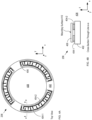
- FIGS. 7A-B depict schematic drawings of top and cross-section views, respectively, of a mask chuck in accordance with an embodiment of the present invention.
- Mask chuck 700 includes mask chuck 206 and support grid 702.
- Support grid 702 includes plate 704 and support ribs 706.
- Plate 704 is a rigid plate from which support ribs 706 extend. In some embodiments, plate 704 and support ribs 706 are machined from a solid body of structural material. Materials suitable for use in plate 704 and support ribs 706 include, without limitation, metals, plastics, ceramics, composite materials, glasses, and the like. Plate 704 is designed to mount to frame 402 to locate support grid 702 within opening 408 such that it mechanically supports membrane 226 when shadow mask 106 is mounted in mask chuck 700.
- Support ribs 706 are arranged to support shadow mask 106 in regions that lie between the through-holes of through-hole arrangement 228.
- the through-holes of a shadow mask are arranged in clusters that correspond to different die regions on the substrate. Since these die regions are usually separated by "lanes" intended for removal by a dicing saw, support ribs 706 are preferably arranged to match the arrangement of these lanes. It should be noted, however, that any suitable arrangement of support ribs can be used in support grid 702.
- Support grid 702 is formed such that their top surfaces 708 are coplanar and define plane 710. Plane 710 lies above mounting surface 410 by a distance equal to the thickness of frame 224. As a result, when frame 224 is in contact with mounting surface 410, support ribs 706 are in contact with membrane 226.
- shadow mask 106 is held upside down in mask chuck 700 such that membrane 226 is in contact with mounting surface 410.
- support grid 702 is designed to fit within opening 408 such that plane 710 is coplanar with mounting surface 410.
- membrane 226 is supported by support grid 702 such that it is perfectly level all the way across opening 408.
- substrate 102 is mounted in substrate chuck 204.
- Substrate chuck 204 is a platen for holding substrate 102 via an attractive force applied only to its back surface.
- substrate chuck 204 generates electrostatic force to hold a substrate; however, in some embodiments, substrate chuck 204 holds a substrate via a different attractive force, such as a vacuum-generated force, a magnetic force, etc.
- magnetic force includes any force arising from the use of permanent magnets and/or electromagnets. Substrate chuck 204 is described in more detail below and with respect to FIGS. 8A-B .
- substrate chuck 204 is dimensioned and arranged to contact substrate 102 only from the front surface to mitigate interference with the deposition of material on the other side of the substrate. In some embodiments, substrate chuck 204 secures the substrate via a different means, such as vacuum, mechanical clamps, from both sides of the substrate, etc. In some embodiments, substrate chuck 204 includes in-situ gap sensors that operate, with positioning system 212 to control the spacing and degree of parallelism between substrate 102 and shadow mask 106.
- substrate 102 is a glass substrate suitable for use in active-matrix organic-light-emitting-diode (AMOLED) displays.
- Substrate 102 includes two major surfaces - back surface 115 and front surface 114, on which the display elements are defined.
- Front surface 114 defines plane 108.
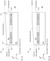
- FIG. 8A depicts a schematic drawing of a cross-sectional view of a substrate chuck in accordance with the illustrative embodiment.
- Substrate chuck 204 includes platen 802 and electrodes 804-1 and 804-2.
- Platen 802 is a structurally rigid platform comprising substrate 806 and dielectric layer 808.
- substrate 806 and dielectric layer 808 includes an electrically insulating material, such as glass, ceramic, anodized aluminum, composite materials, Bakelite, and the like to electrically isolate electrodes 804-1 and 804-2 from each other and from substrate 102 when it is mounted in the substrate chuck.
- Electrodes 804-1 and 804-2 are electrically conductive elements formed on the surface of substrate 806 and overcoated by dielectric layer 808 to embed them within platen 802. Electrodes 804-1 and 804-2 are electrically coupled with controller 240. It should be noted that electrodes 804-1 and 804-2 are depicted as simple plates; however, in practice, substrate chuck 204 can have electrodes that are shaped in any manner, such as interdigitated comb fingers, concentric rings, irregular shapes, etc.
- Dielectric layer 808 is a structurally rigid layer of glass disposed over electrodes 804-1 and 804-2 to give rise to mounting surface 810.
- FIG. 8B depicts a schematic drawing of a cross-sectional view of substrate chuck 204 while holding substrate 102.
- control signal 236 To hold substrate 102 in substrate chuck 204, control signal 236 generates a voltage potential between electrodes 804-1 and 804-2.
- mounting surface 810 i.e. , the top surface of dielectric layer 808
- sympathetic charge regions develop within substrate 102 as shown.
- an electrostatic force is selectively imparted on back surface 115, thereby attracting it to mounting surface 810.
- the illustrative embodiment includes a substrate chuck that holds substrate 102 via electrostatic force
- a substrate is held in a substrate chuck via an attractive force other than an electrostatic force, such as a vacuum-generated force, a magnetic force, and the like.
- the relative positions of substrate 102, source 104, shadow mask 106, and collimator 208 are controlled by positioning system 212.
- Positioning system 212 aligns substrate 102 and shadow mask 106 by controlling the position of substrate chuck 204. In some embodiments, positioning system aligns the substrate and shadow mask by controlling the position of mask chuck 206. In some embodiments, the positions of both chucks is controlled to align the substrate and shadow mask. Operation 304 and positioning system 212 are described in more detail below and with respect to FIGS. 1 , 2 , 9 , 10 and 11A-C .
- the positioning system includes three six-axis manipulators and an optical alignment system to control the alignment between substrate 102 and shadow mask 106.
- Each of the six-axis manipulators is operatively connected with each of substrate chuck 204, mask chuck 206, and collimator chuck 210 to control its position along and rotation about each of the x-, y-, and z-axes.
- the position of at least one of mask chuck 206 and collimator chuck 210 is not controlled by a six-axis positioner.
- positioning system 212 also includes a rotation stage for controlling the relative rotational alignment of substrate 102 and shadow mask 106.
- positioning system 212 locates the substrate and shadow mask such that deposition sites, R, in deposition region 216 are aligned with apertures 120, planes 108 and 118 are parallel and the separation, s, between the substrate and shadow mask is as close to zero ( i.e ., in contact) as possible - preferably within a few microns ( e . g ., 1-5 microns). In some embodiments, s is another suitable separation distance. It should be noted that, for clarity, separation, s, is depicted larger than is typical.
- neither substrate chuck 204 nor mask chuck 206 includes any structural element that projects past its respective mounting surface.
- a substrate and shadow mask can be aligned with little or no separation between them to mitigate feathering during deposition.
- the separation between substrate and shadow mask must be at least a few tens, or even hundreds, of microns.
- FIG. 9 depicts a schematic drawing of a cross-sectional view of a portion of system 100 with substrate 102 and shadow mask 106 in alignment for deposition of material 116.
- Region 902 When the substrate and shadow mask are aligned, they collectively define region 902 between them.
- Region 902 has a lateral extent, L1, which is equal to that of front surface 114.
- Region 902 also has a thickness that is equal to the separation, s1, between planes 108 and 118 (i.e., the separation between the substrate and the shadow mask).
- source 104 generates vapor plume 124.
- the propagation angles, ⁇ p, of the vaporized atoms of vapor plume 124 span a relatively large angular range of - ⁇ m to + ⁇ m.
- this large angular range exacerbates feathering, which is a function of the lateral and rotation alignments between substrate 102 and shadow mask 106, the separation, s, between them, and the range of propagation angles, ⁇ p, of the vaporized atoms incident on the shadow mask.
- the range of propagation angles for the vaporized atoms that reach the substrate surface is reduced by locating a spatial filter (i.e ., collimator 208 ) in their path from source 104 to shadow mask 106.
- a spatial filter i.e ., collimator 208
- collimator 208 significantly reduces feathering during direct deposition.
- FIG. 10 depicts a schematic drawing of an enlarged view of a pixel region 112 of substrate 102 and its corresponding aperture 120 of shadow mask 106.
- the propagation angles of vaporized atoms passed by shadow mask 106 must be within the acceptable range of - ⁇ a to + ⁇ a.
- the term "acceptable angular range" is defined as the range of propagation angles that is desired to be passed by the shadow mask, which spans the angular range from - ⁇ a to + ⁇ a.
- the acceptable angular range is that range of angles that enables material 116 to deposit only on deposition sites R after passing through apertures 120.
- the acceptable angular range includes a small guard band around the deposition sites to allow for feathering that is less than half the spacing between the closest deposition sites. Any vaporized atom incident on the shadow mask having a propagation angle outside this range would deposit on surface 114 beyond the lateral extent of deposition site R.
- vapor plume 124 is filtered by collimator 208 to give rise to vapor column 214.
- FIG. 11A depicts a schematic drawing of a cross-sectional view of a collimator in accordance with the illustrative embodiment.
- Collimator 208 includes body 1102, which is patterned to form a plurality of channels 1104, each of which extends through the thickness of body 1102.
- Body 1102 is a glass plate suitable for planar processing.
- body 1102 has a thickness of approximately 25 millimeters (mm); however, any practical thickness can be used without departing from the scope of the present invention.
- body 1102 comprises a different structurally rigid material that is suitable for withstanding the temperatures associated with thermal and/or e-beam evaporation without significant deformation.
- Materials suitable for use in body 1102 include, without limitation, semiconductors (e.g., silicon, silicon-carbide, etc .), ceramics ( e.g., alumina, etc .), composite materials ( e.g., carbon fibers, etc .), fiber glass, printed circuit board, metals, polymers ( e.g., polyetheretherketone (PEEK), etc .), and the like.
- semiconductors e.g., silicon, silicon-carbide, etc .
- ceramics e.g., alumina, etc .
- composite materials e.g., carbon fibers, etc .
- fiber glass e.g., printed circuit board, metals, polymers (e.g., polyetheretherketone (PEEK), etc .), and the like.
- PEEK polyetheretherketone
- Channels 1104 are through-holes formed in body 1102 using a conventional processing operation, such as metal forming, drilling, electron-discharge machining, deep reactive-ion etching (DRIE), and the like.
- channels 1104 have a circular cross-section with a diameter of approximately 3 mm.
- the height-to-width aspect ratio is at least equal to 3:1.
- the flow of vaporized atoms through the collimator begins to diminish to undesirable levels; however, height-to-width aspect ratios in excess of 100:1 are within the scope of the present invention.
- channels 1104 have a cross-sectional shape other than circular ( e.g., square, rectangular, hexagonal, octagonal, irregular, etc .).
- channels 1104 give rise to a plurality of walls 1106, which reside between the channels.
- walls 1106 are as thin as possible without sacrificing the structural integrity of body 1102.
- walls 506 have an average thickness of approximately 500 microns; however, any practical thickness can be used for walls 1106.
- FIGS. 11B-C depict schematic drawings of top and sectional views, respectively, of a region of collimator 208.
- Channels 1106 are arranged in a honeycomb arrangement wherein columns are periodic and adjacent columns are offset from their neighbors by a half period.
- the channels are arranged in a different arrangement, such as two-dimensional periodic, hexagonally close-packed, random, and the like.
- the aspect ratio of channel 1104 defines a filtered angular range.
- filtered angular range is defined as the range of propagation angles that will pass through collimator 208 , which spans the angular range from - ⁇ c to + ⁇ c .
- will be blocked by the collimator.
- body 1102 channels 1104, and walls 1106 are merely exemplary and that other dimensions can be used without departing from the scope of the present invention.
- apertures 120 pass vaporized atoms of vapor column 214 such that they deposit on deposition sites R in deposition region 216.
- positioning system 212 imparts motion on collimator 208 to improve the uniformity of vaporized-atom density across the lateral extent of vapor column 214, thereby improving the deposition uniformity across the deposition sites on substrate 102.
- positioning system 212 is operative for imparting an oscillating motion to collimator 208.
- source 104 is substantially a point source for material 116 because the open area of its crucible is significantly smaller than the area of substrate 102.
- positioning system 212 moves source 102 in the x-y plane, relative to the substrate, to improve deposition uniformity.
- source 104 is a linear evaporation source that comprises a plurality of nozzles that emits a fan-shaped vapor plume of vaporized atoms.
- positioning system 212 moves the linear source along a direction that is unaligned with its longitudinal axis in the x-y plane to improve the uniformity of the deposited material on substrate 102.
- this path is a line that is substantially orthogonal to both the linear arrangement of nozzles and normal axis 110.
- the linear source is moved along a non-linear path in the x-y plane.
- source 104 includes a two-dimensional arrangement of nozzles, each of which emits a conically shaped vapor plume such that the plurality of nozzles collectively provides a flow of vaporized atoms that is substantially uniform over the area of the substrate surface.
- positioning system 212 moves the two-dimensional arrangement of nozzles to facilitate deposition uniformity.
- the two-dimensional arrangement of nozzles is rotated in-plane to facilitate deposition uniformity.
- source 104 is a two-dimensional planar source that includes a layer of material 116 distributed across its top surface. The source is arranged such that this top surface is parallel to and facing substrate 102. When heated, material 116 vaporizes uniformly across the plane.
- Exemplary planar evaporation sources suitable for use in embodiments of the present invention are disclosed by Tung, et al., in "OLED Fabrication by Using a Novel Planar Evaporation Technique," Int. J. of Photoenergy, Vol. 2014(18), pp. 1-8 (2014 ), which is incorporated herein by reference.
- positioning system 212 imparts a relative motion between source 104 and the combination of substrate 102 and shadow mask 106 by moving at least one of the substrate/mask combination and the source.
Landscapes
- Chemical & Material Sciences (AREA)
- Engineering & Computer Science (AREA)
- Organic Chemistry (AREA)
- Materials Engineering (AREA)
- Mechanical Engineering (AREA)
- Metallurgy (AREA)
- Chemical Kinetics & Catalysis (AREA)
- Manufacturing & Machinery (AREA)
- Health & Medical Sciences (AREA)
- Toxicology (AREA)
- Physics & Mathematics (AREA)
- General Physics & Mathematics (AREA)
- Physical Vapour Deposition (AREA)
- Electroluminescent Light Sources (AREA)
Claims (11)
- System (200) zum Abscheiden eines ersten Materials (116) auf einer Vielzahl von Abscheidungsstellen (R) in einem Abscheidungsbereich (216) eines Substrats (102), wobei die Vielzahl von Abscheidungsstellen in einer ersten Anordnung (228) angeordnet ist, wobei das Substrat eine erste Hauptoberfläche (115) und eine zweite Hauptoberfläche (114) aufweist, die den Abscheidungsbereich umfasst, wobei das System umfasst:eine Quelle (104) zum Bereitstellen einer ersten Vielzahl (124) von verdampften Atomen (122) des ersten Materials, wobei sich jedes verdampfte Atom der ersten Vielzahl davon entlang einer Ausbreitungsrichtung (126) ausbreitet, die durch einen Ausbreitungswinkel (Θρ) relativ zu einer ersten Richtung (128) gekennzeichnet ist, die senkrecht zu einer ersten, durch das Substrat definierten Ebene (108) ist, wobei der Bereich von Ausbreitungswinkeln der ersten Vielzahl von verdampften Atomen einen ersten Winkelbereich (-Om bis +Θm) überspannt;eine Schattenmaske (106), umfassend (i) ein Manipulationssubstrat (224) mit einer ersten Dicke, einer zentralen Öffnung und einer dritten Hauptoberfläche (232) und (ii) eine Membran (226), die über der zentralen Öffnung aufgehängt ist, wobei die Membran eine Vielzahl von Durchgangslöchern (120), die in der ersten Anordnung (228) angeordnet sind, und eine vierte Hauptoberfläche (230) aufweist;ein erstes Spannfutter (204) zum Halten des Substrats, wobei das erste Spannfutter so dimensioniert und angeordnet ist, dass es selektiv eine erste Anziehungskraft auf die erste Hauptoberfläche ausübt;ein zweites Spannfutter (700) zum Halten der Schattenmaske, wobei das zweite Spannfutter einen Rahmen (402) umfasst, der eine erste Öffnung (408) umgibt, die es dem Material ermöglicht, durch das zweite Spannfutter zu den Durchgangslöchern zu gelangen, wobei der Rahmen eine Montagefläche (410) umfasst, die die erste Öffnung umgibt und in einer zweiten Ebene (610) liegt, wobei die Montagefläche in Kontakt mit der dritten Hauptoberfläche ist, wenn die Schattenmaske in dem zweiten Spannfutter gehalten wird;einen Kollimator (208) mit einer Vielzahl von Kanälen (1104), wobei der Kollimator zwischen der Quelle und der Schattenmaske ist, und wobei jeder Kanal der Vielzahl von Kanälen so dimensioniert und angeordnet ist, dass er nur verdampfte Atome mit einem Ausbreitungswinkel innerhalb eines zweiten Winkelbereichs (-Oc bis +Oc) durchlässt, der kleiner ist als der erste Winkelbereich; undein Positionierungssystem (212) zum Steuern der relativen Position des ersten Spannfutters und des zweiten Spannfutters zum Ausrichten der Schattenmaske und des Substrats;DADURCH GEKENNZEICHNET, DASS:
das zweite Spannfutter ferner ein Stützgitter (702) umfasst, das in der ersten Öffnung angeordnet ist, wobei das Stützgitter an dem Rahmen (402) über eine Platte (704) befestigt ist und eine Vielzahl von Stützrippen (706) umfasst, wobei jede Stützrippe eine obere Fläche (708) aufweist, die in einer dritten Ebene (710) liegt, die von der zweiten Ebene in einem Abstand, der der ersten Dicke entspricht, getrennt ist, und wobei die Stützrippen durch die zentrale Öffnung erstrecken und die Membran mechanisch abstützen, wenn die Schattenmaske in das zweite Spannfutter montiert ist. - Das System nach Anspruch 1, wobei der Rahmen kreisförmig ist.
- System nach Anspruch 1, bei dem die Vielzahl von Abscheidungsstellen und die Vielzahl von Durchgangslöchern gemeinsam einen akzeptablen Winkelbereich (Θa bis +Θa) definieren, wobei der zweite Winkelbereich kleiner oder gleich dem akzeptablen Winkelbereich ist.
- System nach Anspruch 1, wobei jeder der Vielzahl von Kanälen durch ein Seitenverhältnis von Höhe zu Breite gekennzeichnet ist, das gleich oder größer als 8:1 ist.
- System nach Anspruch 1, bei dem das Positionierungssystem eine relative Bewegung zwischen dem Substrat und dem Kollimator bewirkt.
- System nach Anspruch 1, wobei das erste Spannfutter, das zweite Spannfutter und das Ausrichtungssystem gemeinsam die Ausrichtung des Substrats und der Schattenmaske mit einem Abstand zwischen ihnen ermöglichen, der größer als 0 Mikrometer und kleiner als oder gleich etwa 10 Mikrometer ist.
- System nach Anspruch 1, wobei das zweite Spannfutter so dimensioniert und angeordnet ist, dass es den durch die Schwerkraft verursachten Durchhang der Schattenmaske abschwächt.
- Verfahren zum Abscheiden eines ersten Materials (116) auf einer Vielzahl von Abscheidungsstellen (R), die in einer ersten Anordnung (228) auf einem Substrat (102) angeordnet sind, wobei das Substrat eine erste Hauptoberfläche (115) und eine zweite Hauptoberfläche (114) mit einer ersten seitlichen Ausdehnung (L1) aufweist, und wobei die zweite Hauptoberfläche einen ersten Bereich (216) umfasst, und wobei das Verfahren umfasst:Bereitstellen einer Schattenmaske (106), umfassend (i) ein Manipulationssubstrat (224) mit einer ersten Dicke, einer zentralen Öffnung und einer dritten Hauptoberfläche (232) und (ii) eine Membran (226), die über der zentralen Öffnung aufgehängt ist, wobei die Membran eine Vielzahl von Durchgangslöchern (120), die in der ersten Anordnung angeordnet sind, und eine vierte Hauptoberfläche (230) aufweist;Halten des Substrats in einem ersten Spannfutter (204), das selektiv eine erste Anziehungskraft auf die erste Hauptoberfläche ausübt;Halten der Schattenmaske in einem zweiten Spannfutter (700), das eine zweite Anziehungskraft selektiv auf die dritte Hauptoberfläche ausübt, wobei das zweite Spannfutter einen Rahmen (402) mit einer ersten Öffnung (408) aufweist, die den Durchgang von verdampften Atomen des Materials durch das zweite Spannfutter zu der Vielzahl von Durchgangslöchern ermöglicht, wobei der Rahmen eine Montagefläche (410) aufweist, die die erste Öffnung umgibt und die in einer ersten Ebene (610) liegt, wobei die Montagefläche in Kontakt mit der dritten Hauptoberfläche ist, wenn die Schattenmaske in dem zweiten Spannfutter gehalten wird;Positionieren des Substrats und der Schattenmaske derart, dass die zweite Hauptoberfläche und die vierte Hauptoberfläche durch einen Abstand getrennt werden, der kleiner als oder gleich 10 Mikrometer ist;Empfangen einer ersten Vielzahl (124) von verdampften Atomen (122) an einem Kollimator (208), der sich zwischen einer Quelle und der Schattenmaske befindet, wobei die erste Vielzahl von verdampften Atomen durch einen ersten Bereich von Ausbreitungswinkeln (-Θm bis +Θm) gekennzeichnet ist;selektives Leiten einer zweiten Vielzahl (214) von verdampften Atomen durch den Kollimator zur Schattenmaske, wobei die erste Vielzahl von verdampften Atomen die zweite Vielzahl von verdampften Atomen einschließt, und wobei die zweite Vielzahl von verdampften Atomen durch einen zweiten Bereich von Ausbreitungswinkeln (-Oc bis +Θc) gekennzeichnet ist, der enger ist als der erste Bereich von Ausbreitungswinkeln; undErmöglichen, dass zumindest einige der zweiten Vielzahl von verdampften Atomen durch das zweite Spannfutter und die Vielzahl von Durchgangslöchern hindurchgehen, um sich auf dem Substrat abzulagern;DADURCH GEKENNZEICHNET, DASS:
das zweite Spannfutter ein Stützgitter (702) umfasst, das sich in der ersten Öffnung befindet, wobei das Stützgitter über eine Platte (704) an dem Rahmen befestigt ist und eine Vielzahl von Stützrippen (706) umfasst, wobei jede Stützrippe eine obere Fläche (708) aufweist, die sich in einer zweiten Ebene (710) befindet, die von der ersten Ebene durch einen Abstand getrennt ist, der gleich der ersten Dicke ist, und wobei sich die Stützrippen durch die zentrale Öffnung erstrecken und die Membran mechanisch stützen, um ein schwerkraftbedingtes Durchhängen der Schattenmaske zu verringern, wenn die Schattenmaske in dem zweiten Spannfutter montiert wird. - Das Verfahren nach Anspruch 8, ferner umfassend das Bereitstellen des Kollimators in der Weise, dass er eine Vielzahl von Kanälen (1104) umfasst, wobei jeder Kanal der Vielzahl von Kanälen ein Seitenverhältnis von Höhe zu Breite aufweist, das den zweiten Bereich von Ausbreitungswinkeln bestimmt, und wobei das Seitenverhältnis von Höhe zu Breite auf einem akzeptablen Winkelbereich (-Θa bis +Θa) basiert, wobei der akzeptable Winkelbereich durch das Substrat und die Schattenmaske definiert ist.
- Verfahren nach Anspruch 8, bei dem das Substrat und die Schattenmaske so ausgerichtet sind, dass die zweite Hauptoberfläche und die vierte Hauptoberfläche durch einen Abstand getrennt werden, der größer als 0 Mikrometer und kleiner als oder gleich 10 Mikrometer ist.
- Verfahren nach Anspruch 8, ferner umfassend das Bereitstellen des zweiten Spannfutters derart, dass der Rahmen kreisförmig ist.
Applications Claiming Priority (4)
| Application Number | Priority Date | Filing Date | Title |
|---|---|---|---|
| US201662340793P | 2016-05-24 | 2016-05-24 | |
| US15/597,635 US10072328B2 (en) | 2016-05-24 | 2017-05-17 | High-precision shadow-mask-deposition system and method therefor |
| US15/602,939 US10386731B2 (en) | 2016-05-24 | 2017-05-23 | Shadow-mask-deposition system and method therefor |
| PCT/IB2017/054481 WO2017203502A2 (en) | 2016-05-24 | 2017-07-24 | High-precision shadow-mask-deposition system and method therefor |
Publications (3)
| Publication Number | Publication Date |
|---|---|
| EP3464672A2 EP3464672A2 (de) | 2019-04-10 |
| EP3464672A4 EP3464672A4 (de) | 2020-01-29 |
| EP3464672B1 true EP3464672B1 (de) | 2024-07-17 |
Family
ID=60412162
Family Applications (1)
| Application Number | Title | Priority Date | Filing Date |
|---|---|---|---|
| EP17802312.3A Active EP3464672B1 (de) | 2016-05-24 | 2017-07-24 | Hochpräzises schattenmaskenabscheidungssystem und verfahren dafür |
Country Status (4)
| Country | Link |
|---|---|
| US (1) | US11275315B2 (de) |
| EP (1) | EP3464672B1 (de) |
| TW (2) | TWI721170B (de) |
| WO (1) | WO2017203502A2 (de) |
Families Citing this family (16)
| Publication number | Priority date | Publication date | Assignee | Title |
|---|---|---|---|---|
| US10644239B2 (en) | 2014-11-17 | 2020-05-05 | Emagin Corporation | High precision, high resolution collimating shadow mask and method for fabricating a micro-display |
| US10072328B2 (en) | 2016-05-24 | 2018-09-11 | Emagin Corporation | High-precision shadow-mask-deposition system and method therefor |
| TWI721170B (zh) | 2016-05-24 | 2021-03-11 | 美商伊麥傑公司 | 蔽蔭遮罩沉積系統及其方法 |
| US10386731B2 (en) | 2016-05-24 | 2019-08-20 | Emagin Corporation | Shadow-mask-deposition system and method therefor |
| JP2018170152A (ja) * | 2017-03-29 | 2018-11-01 | Tianma Japan株式会社 | Oled表示装置の製造方法、マスク及びマスクの設計方法 |
| US10886452B2 (en) * | 2018-01-25 | 2021-01-05 | United States Of America As Represented By The Administrator Of Nasa | Selective and direct deposition technique for streamlined CMOS processing |
| CN108198958B (zh) * | 2018-01-30 | 2020-06-30 | 京东方科技集团股份有限公司 | 显示基板及其制作方法、制作设备、显示装置 |
| KR20200017381A (ko) * | 2018-08-06 | 2020-02-18 | 어플라이드 머티어리얼스, 인코포레이티드 | 마스크 정렬기를 갖는 증착 장치, 기판을 마스킹하기 위한 마스크 어레인지먼트, 및 기판을 마스킹하기 위한 방법 |
| US11056277B2 (en) | 2018-12-28 | 2021-07-06 | Applied Materials, Inc. | Magnetized substrate carrier apparatus with shadow mask for deposition |
| US20210054497A1 (en) * | 2019-08-19 | 2021-02-25 | Oem Group, Llc | Systems and methods for a lift and rotate wafer handling process |
| DE102020109265A1 (de) * | 2020-04-02 | 2021-10-07 | Apeva Se | Substrathalter mit einer elastischen Substratauflage |
| KR102787867B1 (ko) * | 2020-07-03 | 2025-04-01 | 삼성디스플레이 주식회사 | 표시 장치의 제조 장치 및 표시 장치의 제조 방법 |
| CN112662995A (zh) * | 2020-12-24 | 2021-04-16 | 京东方科技集团股份有限公司 | 一种掩膜板和掩膜板制作方法 |
| KR20230140665A (ko) * | 2022-03-29 | 2023-10-10 | 삼성디스플레이 주식회사 | 증착 마스크 스테이지, 이를 포함하는 디스플레이 제조 장치, 및 이를 이용한 디스플레이 제조 방법 |
| US20240081135A1 (en) * | 2022-09-06 | 2024-03-07 | Emagin Corporation | Rigid Sapphire Based Direct Patterning Deposition Mask |
| KR20250122025A (ko) * | 2024-02-05 | 2025-08-13 | 삼성디스플레이 주식회사 | 표시 장치의 제조장치 및 표시 장치의 제조 방법 |
Family Cites Families (74)
| Publication number | Priority date | Publication date | Assignee | Title |
|---|---|---|---|---|
| US4393131A (en) | 1982-03-29 | 1983-07-12 | Motorola, Inc. | Method for captivating a substrate within a holder |
| RU2032765C1 (ru) | 1987-04-03 | 1995-04-10 | Фудзицу Лимитед | Способ нанесения алмазного покрытия из паровой фазы и устройство для его осуществления |
| US4902377A (en) | 1989-05-23 | 1990-02-20 | Motorola, Inc. | Sloped contact etch process |
| JPH03104865A (ja) | 1989-09-16 | 1991-05-01 | Toshiba Corp | 蒸着装置 |
| US5013275A (en) * | 1990-01-02 | 1991-05-07 | Zenith Electronics Corporation | Continuous laser beam FTM mounting for CRT |
| JPH06330309A (ja) | 1993-05-20 | 1994-11-29 | Nippon Steel Corp | コリメートスパッタ法による成膜方法及び装置 |
| JPH0729814A (ja) | 1993-07-07 | 1995-01-31 | Nippon Telegr & Teleph Corp <Ntt> | マスク基板保持機構 |
| JPH0741943A (ja) | 1993-07-27 | 1995-02-10 | Nec Corp | スパッタ装置 |
| JP2833979B2 (ja) | 1993-11-26 | 1998-12-09 | 日本電気株式会社 | コリメートを有するスパッタ装置 |
| JPH07316808A (ja) | 1994-05-27 | 1995-12-05 | Nippon Steel Corp | スパッタリング装置 |
| US5854819A (en) * | 1996-02-07 | 1998-12-29 | Canon Kabushiki Kaisha | Mask supporting device and correction method therefor, and exposure apparatus and device producing method utilizing the same |
| JP3814359B2 (ja) * | 1996-03-12 | 2006-08-30 | キヤノン株式会社 | X線投影露光装置及びデバイス製造方法 |
| JPH1050584A (ja) * | 1996-08-07 | 1998-02-20 | Nikon Corp | マスク保持装置 |
| US6069931A (en) | 1997-02-28 | 2000-05-30 | Canon Kabushiki Kaisha | Mask structure and mask holding mechanism for exposure apparatus |
| US6287436B1 (en) | 1998-02-27 | 2001-09-11 | Innovent, Inc. | Brazed honeycomb collimator |
| US7282240B1 (en) | 1998-04-21 | 2007-10-16 | President And Fellows Of Harvard College | Elastomeric mask and use in fabrication of devices |
| US6592728B1 (en) | 1998-08-04 | 2003-07-15 | Veeco-Cvc, Inc. | Dual collimated deposition apparatus and method of use |
| RU2155204C2 (ru) | 1998-09-23 | 2000-08-27 | Институт проблем химической физики РАН | Органический электролюминесцентный материал, излучающий в красной области спектра |
| JP2001118776A (ja) * | 1999-10-19 | 2001-04-27 | Nikon Corp | 転写型露光装置および該装置に使用されるマスク保持機構、および半導体素子の製造方法。 |
| DE10039644A1 (de) | 2000-08-14 | 2002-02-28 | Rubitec Gesellschaft Fuer Innovation & Technologie Ruhr Univ Bochum Mbh | Lochmaske und Verfahren zur Herstellung einer Lochmaske |
| CA2421520A1 (en) | 2000-09-22 | 2002-03-28 | General Electric Company | Combinatorial coating systems and methods |
| JP2002352745A (ja) | 2001-05-30 | 2002-12-06 | Hitachi Ltd | カラー陰極線管 |
| TWI252706B (en) | 2002-09-05 | 2006-04-01 | Sanyo Electric Co | Manufacturing method of organic electroluminescent display device |
| JP2004119064A (ja) | 2002-09-24 | 2004-04-15 | Fujitsu Ltd | 薄膜形成装置および薄膜形成方法 |
| US20040086639A1 (en) | 2002-09-24 | 2004-05-06 | Grantham Daniel Harrison | Patterned thin-film deposition using collimating heated mask asembly |
| JP2004183044A (ja) | 2002-12-03 | 2004-07-02 | Seiko Epson Corp | マスク蒸着方法及び装置、マスク及びマスクの製造方法、表示パネル製造装置、表示パネル並びに電子機器 |
| JP2004207572A (ja) * | 2002-12-26 | 2004-07-22 | Toshiba Corp | ステンシルマスク及びマスク形成用基板並びにステンシルマスクの製造方法及びマスク形成用基板の製造方法 |
| US20050212419A1 (en) | 2004-03-23 | 2005-09-29 | Eastman Kodak Company | Encapsulating oled devices |
| JP4860909B2 (ja) | 2004-05-25 | 2012-01-25 | キヤノン株式会社 | マスク構造体 |
| US7863632B2 (en) | 2004-08-23 | 2011-01-04 | National Research Council Of Canada | High performance light-emitting devices |
| US7239376B2 (en) * | 2005-07-27 | 2007-07-03 | International Business Machines Corporation | Method and apparatus for correcting gravitational sag in photomasks used in the production of electronic devices |
| US7615161B2 (en) | 2005-08-19 | 2009-11-10 | General Electric Company | Simplified way to manufacture a low cost cast type collimator assembly |
| US7236324B2 (en) | 2005-10-18 | 2007-06-26 | Hitachi Global Storage Technologies | Apparatus, method and system for fabricating servo patterns on high density patterned media |
| US7393758B2 (en) | 2005-11-03 | 2008-07-01 | Maxim Integrated Products, Inc. | Wafer level packaging process |
| US7741770B2 (en) | 2007-10-05 | 2010-06-22 | Global Oled Technology Llc | LED device having improved light output |
| US7977868B2 (en) | 2008-07-23 | 2011-07-12 | Cbrite Inc. | Active matrix organic light emitting device with MO TFT backplane |
| US8742658B2 (en) | 2008-07-23 | 2014-06-03 | Cbrite Inc. | Full-color active matrix organic light emitting display with hybrid |
| EP2168644B1 (de) | 2008-09-29 | 2014-11-05 | Applied Materials, Inc. | Verdampfer für organische Materialien und Verfahren zum Verdampfen organischer Materialien |
| JP5642153B2 (ja) | 2009-04-03 | 2014-12-17 | オスラム オプト セミコンダクターズ ゲゼルシャフト ミット ベシュレンクテル ハフツングOsram Opto Semiconductors GmbH | 材料堆積装置において基板を保持する装置 |
| JP5620146B2 (ja) | 2009-05-22 | 2014-11-05 | 三星ディスプレイ株式會社Samsung Display Co.,Ltd. | 薄膜蒸着装置 |
| JP2012052155A (ja) | 2010-08-31 | 2012-03-15 | Canon Inc | 真空成膜用マスクユニット及びこれを備えた真空成膜装置 |
| KR101597887B1 (ko) | 2010-12-20 | 2016-02-25 | 샤프 가부시키가이샤 | 증착 방법 및 증착 장치 |
| CN103238374B (zh) | 2010-12-27 | 2015-06-24 | 夏普株式会社 | 蒸镀装置、蒸镀方法和有机el显示装置 |
| CN103282543B (zh) * | 2011-03-10 | 2014-12-24 | 夏普株式会社 | 蒸镀装置和蒸镀方法 |
| US8728563B2 (en) | 2011-05-03 | 2014-05-20 | Palmaz Scientific, Inc. | Endoluminal implantable surfaces, stents, and grafts and method of making same |
| US8879766B1 (en) | 2011-10-03 | 2014-11-04 | Wei Zhang | Flat panel displaying and sounding system integrating flat panel display with flat panel sounding unit array |
| US20130168231A1 (en) * | 2011-12-31 | 2013-07-04 | Intermolecular Inc. | Method For Sputter Deposition And RF Plasma Sputter Etch Combinatorial Processing |
| US9655199B2 (en) | 2012-05-30 | 2017-05-16 | Universal Display Corporation | Four component phosphorescent OLED for cool white lighting application |
| US20130344612A1 (en) | 2012-06-20 | 2013-12-26 | The Research Foundation Of State University Of New York | Ultrasensitive, superfast, and microliter-volume differential scanning nanocalorimeter for direct charactization of biomolecular interactions |
| US20150299840A1 (en) | 2012-06-26 | 2015-10-22 | Sharp Kabushiki Kaisha | Mask frame |
| US8940568B2 (en) | 2012-08-31 | 2015-01-27 | Universal Display Corporation | Patterning method for OLEDs |
| KR102100446B1 (ko) | 2012-12-10 | 2020-04-14 | 삼성디스플레이 주식회사 | 박막 증착용 마스크 조립체 및 이의 제조 방법 |
| CN203159695U (zh) | 2013-01-22 | 2013-08-28 | 昆山允升吉光电科技有限公司 | 一种蒸镀用掩模组件 |
| JP6068514B2 (ja) | 2013-01-29 | 2017-01-25 | シャープ株式会社 | 蒸着ユニットおよび蒸着装置 |
| KR102079170B1 (ko) | 2013-04-09 | 2020-02-20 | 삼성디스플레이 주식회사 | 증착 장치 및 그에 적용되는 마스크 조립체 |
| KR101765018B1 (ko) | 2013-07-08 | 2017-08-03 | 샤프 가부시키가이샤 | 증착 장치, 증착 방법 및 유기 일렉트로 루미네센스 소자의 제조 방법 |
| US9142779B2 (en) | 2013-08-06 | 2015-09-22 | University Of Rochester | Patterning of OLED materials |
| JP6363333B2 (ja) * | 2013-08-07 | 2018-07-25 | シャープ株式会社 | 蒸着装置、及び、有機エレクトロルミネッセンス素子の製造方法 |
| JP5846287B1 (ja) * | 2013-12-27 | 2016-01-20 | 大日本印刷株式会社 | フレーム付き蒸着マスクの製造方法、引張装置、有機半導体素子の製造装置及び有機半導体素子の製造方法 |
| JP6511908B2 (ja) * | 2014-03-31 | 2019-05-15 | 大日本印刷株式会社 | 蒸着マスクの引張方法、フレーム付き蒸着マスクの製造方法、有機半導体素子の製造方法、及び引張装置 |
| US20150275351A1 (en) | 2014-04-01 | 2015-10-01 | Apple Inc. | Evaporation Tool |
| JP6429491B2 (ja) * | 2014-05-13 | 2018-11-28 | シャープ株式会社 | 蒸着装置用マスク、蒸着装置、蒸着方法、及び、有機エレクトロルミネッセンス素子の製造方法 |
| JP6278833B2 (ja) | 2014-05-21 | 2018-02-14 | キヤノン株式会社 | リソグラフィ装置、および物品の製造方法 |
| US20170104158A1 (en) | 2014-06-05 | 2017-04-13 | Sharp Kabushiki Kaisha | Vapor deposition method and vapor deposition apparatus |
| RU2588921C2 (ru) | 2014-09-25 | 2016-07-10 | Общество С Ограниченной Ответственностью "Ласком" | Способ формирования токоведущей шины на низкоэмиссионной поверхности стекла |
| US10115573B2 (en) | 2014-10-14 | 2018-10-30 | Applied Materials, Inc. | Apparatus for high compressive stress film deposition to improve kit life |
| JP6442994B2 (ja) | 2014-11-10 | 2018-12-26 | トヨタ自動車株式会社 | マスク吸着装置 |
| US10644239B2 (en) | 2014-11-17 | 2020-05-05 | Emagin Corporation | High precision, high resolution collimating shadow mask and method for fabricating a micro-display |
| KR102318264B1 (ko) * | 2015-01-14 | 2021-10-27 | 삼성디스플레이 주식회사 | 증착장치 |
| CN104911548B (zh) | 2015-06-30 | 2017-05-03 | 合肥鑫晟光电科技有限公司 | 一种真空蒸镀装置及蒸镀方法 |
| TWI721170B (zh) | 2016-05-24 | 2021-03-11 | 美商伊麥傑公司 | 蔽蔭遮罩沉積系統及其方法 |
| US10386731B2 (en) | 2016-05-24 | 2019-08-20 | Emagin Corporation | Shadow-mask-deposition system and method therefor |
| US10072328B2 (en) | 2016-05-24 | 2018-09-11 | Emagin Corporation | High-precision shadow-mask-deposition system and method therefor |
| CN106637087B (zh) * | 2016-11-18 | 2019-05-17 | 上海天马微电子有限公司 | 蒸镀设备 |
-
2017
- 2017-05-24 TW TW106117272A patent/TWI721170B/zh active
- 2017-05-24 TW TW106117271A patent/TWI633197B/zh active
- 2017-07-20 US US15/655,544 patent/US11275315B2/en active Active
- 2017-07-24 EP EP17802312.3A patent/EP3464672B1/de active Active
- 2017-07-24 WO PCT/IB2017/054481 patent/WO2017203502A2/en not_active Ceased
Also Published As
| Publication number | Publication date |
|---|---|
| WO2017203502A2 (en) | 2017-11-30 |
| TW201807221A (zh) | 2018-03-01 |
| US20170342543A1 (en) | 2017-11-30 |
| TWI633197B (zh) | 2018-08-21 |
| EP3464672A2 (de) | 2019-04-10 |
| TWI721170B (zh) | 2021-03-11 |
| WO2017203502A3 (en) | 2018-01-04 |
| EP3464672A4 (de) | 2020-01-29 |
| US11275315B2 (en) | 2022-03-15 |
| TW201805456A (zh) | 2018-02-16 |
Similar Documents
| Publication | Publication Date | Title |
|---|---|---|
| EP3464672B1 (de) | Hochpräzises schattenmaskenabscheidungssystem und verfahren dafür | |
| US10072328B2 (en) | High-precision shadow-mask-deposition system and method therefor | |
| US10386731B2 (en) | Shadow-mask-deposition system and method therefor | |
| US20180340252A1 (en) | System and method for reducing attractive forces between a deposition mask and substrate and a deposition system and method utilizing the same | |
| US11968881B2 (en) | Mechanically pre-biased shadow mask and method of formation | |
| CN109642309B (zh) | 高精准度蔽荫掩模沉积系统及其方法 | |
| CN111293067A (zh) | 静电吸盘、静电吸盘系统、成膜装置及方法、吸附方法、电子器件的制造方法 | |
| US11905590B2 (en) | Direct-deposition system including standoffs for controlling substrate-mask separation | |
| US11152573B2 (en) | Shadow mask comprising a gravity-compensation layer and method of fabrication | |
| JP2020070488A (ja) | 静電チャックシステム、成膜装置、吸着方法、成膜方法及び電子デバイスの製造方法 | |
| EP3464674A1 (de) | Hochpräzises schattenmaskenabscheidungssystem und verfahren dafür |
Legal Events
| Date | Code | Title | Description |
|---|---|---|---|
| STAA | Information on the status of an ep patent application or granted ep patent |
Free format text: STATUS: THE INTERNATIONAL PUBLICATION HAS BEEN MADE |
|
| PUAI | Public reference made under article 153(3) epc to a published international application that has entered the european phase |
Free format text: ORIGINAL CODE: 0009012 |
|
| STAA | Information on the status of an ep patent application or granted ep patent |
Free format text: STATUS: REQUEST FOR EXAMINATION WAS MADE |
|
| 17P | Request for examination filed |
Effective date: 20181220 |
|
| AK | Designated contracting states |
Kind code of ref document: A2 Designated state(s): AL AT BE BG CH CY CZ DE DK EE ES FI FR GB GR HR HU IE IS IT LI LT LU LV MC MK MT NL NO PL PT RO RS SE SI SK SM TR |
|
| AX | Request for extension of the european patent |
Extension state: BA ME |
|
| DAV | Request for validation of the european patent (deleted) | ||
| DAX | Request for extension of the european patent (deleted) | ||
| A4 | Supplementary search report drawn up and despatched |
Effective date: 20200108 |
|
| RIC1 | Information provided on ipc code assigned before grant |
Ipc: C23C 14/54 20060101ALI20191220BHEP Ipc: H01L 21/683 20060101ALI20191220BHEP Ipc: H01L 51/00 20060101ALI20191220BHEP Ipc: H01L 21/68 20060101ALI20191220BHEP Ipc: C23C 14/50 20060101ALI20191220BHEP Ipc: C23C 14/58 20060101ALI20191220BHEP Ipc: C23C 14/04 20060101AFI20191220BHEP Ipc: G03F 9/00 20060101ALI20191220BHEP |
|
| STAA | Information on the status of an ep patent application or granted ep patent |
Free format text: STATUS: EXAMINATION IS IN PROGRESS |
|
| 17Q | First examination report despatched |
Effective date: 20230306 |
|
| P01 | Opt-out of the competence of the unified patent court (upc) registered |
Effective date: 20230525 |
|
| RIC1 | Information provided on ipc code assigned before grant |
Ipc: H10K 71/16 20230101ALI20231218BHEP Ipc: H01L 21/683 20060101ALI20231218BHEP Ipc: H01L 21/68 20060101ALI20231218BHEP Ipc: C23C 14/50 20060101ALI20231218BHEP Ipc: C23C 14/04 20060101AFI20231218BHEP |
|
| GRAP | Despatch of communication of intention to grant a patent |
Free format text: ORIGINAL CODE: EPIDOSNIGR1 |
|
| STAA | Information on the status of an ep patent application or granted ep patent |
Free format text: STATUS: GRANT OF PATENT IS INTENDED |
|
| INTG | Intention to grant announced |
Effective date: 20240212 |
|
| GRAS | Grant fee paid |
Free format text: ORIGINAL CODE: EPIDOSNIGR3 |
|
| GRAA | (expected) grant |
Free format text: ORIGINAL CODE: 0009210 |
|
| STAA | Information on the status of an ep patent application or granted ep patent |
Free format text: STATUS: THE PATENT HAS BEEN GRANTED |
|
| AK | Designated contracting states |
Kind code of ref document: B1 Designated state(s): AL AT BE BG CH CY CZ DE DK EE ES FI FR GB GR HR HU IE IS IT LI LT LU LV MC MK MT NL NO PL PT RO RS SE SI SK SM TR |
|
| REG | Reference to a national code |
Ref country code: CH Ref legal event code: EP |
|
| REG | Reference to a national code |
Ref country code: DE Ref legal event code: R096 Ref document number: 602017083384 Country of ref document: DE |
|
| REG | Reference to a national code |
Ref country code: IE Ref legal event code: FG4D |
|
| REG | Reference to a national code |
Ref country code: NL Ref legal event code: FP |
|
| REG | Reference to a national code |
Ref country code: LT Ref legal event code: MG9D |
|
| REG | Reference to a national code |
Ref country code: AT Ref legal event code: UEP Ref document number: 1704204 Country of ref document: AT Kind code of ref document: T Effective date: 20240717 |
|
| PG25 | Lapsed in a contracting state [announced via postgrant information from national office to epo] |
Ref country code: PT Free format text: LAPSE BECAUSE OF FAILURE TO SUBMIT A TRANSLATION OF THE DESCRIPTION OR TO PAY THE FEE WITHIN THE PRESCRIBED TIME-LIMIT Effective date: 20241118 |
|
| PG25 | Lapsed in a contracting state [announced via postgrant information from national office to epo] |
Ref country code: PT Free format text: LAPSE BECAUSE OF FAILURE TO SUBMIT A TRANSLATION OF THE DESCRIPTION OR TO PAY THE FEE WITHIN THE PRESCRIBED TIME-LIMIT Effective date: 20241118 |
|
| PG25 | Lapsed in a contracting state [announced via postgrant information from national office to epo] |
Ref country code: NO Free format text: LAPSE BECAUSE OF FAILURE TO SUBMIT A TRANSLATION OF THE DESCRIPTION OR TO PAY THE FEE WITHIN THE PRESCRIBED TIME-LIMIT Effective date: 20241017 |
|
| PG25 | Lapsed in a contracting state [announced via postgrant information from national office to epo] |
Ref country code: FI Free format text: LAPSE BECAUSE OF FAILURE TO SUBMIT A TRANSLATION OF THE DESCRIPTION OR TO PAY THE FEE WITHIN THE PRESCRIBED TIME-LIMIT Effective date: 20240717 Ref country code: GR Free format text: LAPSE BECAUSE OF FAILURE TO SUBMIT A TRANSLATION OF THE DESCRIPTION OR TO PAY THE FEE WITHIN THE PRESCRIBED TIME-LIMIT Effective date: 20241018 Ref country code: PL Free format text: LAPSE BECAUSE OF FAILURE TO SUBMIT A TRANSLATION OF THE DESCRIPTION OR TO PAY THE FEE WITHIN THE PRESCRIBED TIME-LIMIT Effective date: 20240717 |
|
| PG25 | Lapsed in a contracting state [announced via postgrant information from national office to epo] |
Ref country code: BG Free format text: LAPSE BECAUSE OF FAILURE TO SUBMIT A TRANSLATION OF THE DESCRIPTION OR TO PAY THE FEE WITHIN THE PRESCRIBED TIME-LIMIT Effective date: 20240717 |
|
| PG25 | Lapsed in a contracting state [announced via postgrant information from national office to epo] |
Ref country code: LV Free format text: LAPSE BECAUSE OF FAILURE TO SUBMIT A TRANSLATION OF THE DESCRIPTION OR TO PAY THE FEE WITHIN THE PRESCRIBED TIME-LIMIT Effective date: 20240717 |
|
| PG25 | Lapsed in a contracting state [announced via postgrant information from national office to epo] |
Ref country code: IS Free format text: LAPSE BECAUSE OF FAILURE TO SUBMIT A TRANSLATION OF THE DESCRIPTION OR TO PAY THE FEE WITHIN THE PRESCRIBED TIME-LIMIT Effective date: 20241117 |
|
| PG25 | Lapsed in a contracting state [announced via postgrant information from national office to epo] |
Ref country code: HR Free format text: LAPSE BECAUSE OF FAILURE TO SUBMIT A TRANSLATION OF THE DESCRIPTION OR TO PAY THE FEE WITHIN THE PRESCRIBED TIME-LIMIT Effective date: 20240717 |
|
| PG25 | Lapsed in a contracting state [announced via postgrant information from national office to epo] |
Ref country code: ES Free format text: LAPSE BECAUSE OF FAILURE TO SUBMIT A TRANSLATION OF THE DESCRIPTION OR TO PAY THE FEE WITHIN THE PRESCRIBED TIME-LIMIT Effective date: 20240717 Ref country code: RS Free format text: LAPSE BECAUSE OF FAILURE TO SUBMIT A TRANSLATION OF THE DESCRIPTION OR TO PAY THE FEE WITHIN THE PRESCRIBED TIME-LIMIT Effective date: 20241017 |
|
| PG25 | Lapsed in a contracting state [announced via postgrant information from national office to epo] |
Ref country code: RS Free format text: LAPSE BECAUSE OF FAILURE TO SUBMIT A TRANSLATION OF THE DESCRIPTION OR TO PAY THE FEE WITHIN THE PRESCRIBED TIME-LIMIT Effective date: 20241017 Ref country code: PL Free format text: LAPSE BECAUSE OF FAILURE TO SUBMIT A TRANSLATION OF THE DESCRIPTION OR TO PAY THE FEE WITHIN THE PRESCRIBED TIME-LIMIT Effective date: 20240717 Ref country code: NO Free format text: LAPSE BECAUSE OF FAILURE TO SUBMIT A TRANSLATION OF THE DESCRIPTION OR TO PAY THE FEE WITHIN THE PRESCRIBED TIME-LIMIT Effective date: 20241017 Ref country code: LV Free format text: LAPSE BECAUSE OF FAILURE TO SUBMIT A TRANSLATION OF THE DESCRIPTION OR TO PAY THE FEE WITHIN THE PRESCRIBED TIME-LIMIT Effective date: 20240717 Ref country code: IS Free format text: LAPSE BECAUSE OF FAILURE TO SUBMIT A TRANSLATION OF THE DESCRIPTION OR TO PAY THE FEE WITHIN THE PRESCRIBED TIME-LIMIT Effective date: 20241117 Ref country code: HR Free format text: LAPSE BECAUSE OF FAILURE TO SUBMIT A TRANSLATION OF THE DESCRIPTION OR TO PAY THE FEE WITHIN THE PRESCRIBED TIME-LIMIT Effective date: 20240717 Ref country code: GR Free format text: LAPSE BECAUSE OF FAILURE TO SUBMIT A TRANSLATION OF THE DESCRIPTION OR TO PAY THE FEE WITHIN THE PRESCRIBED TIME-LIMIT Effective date: 20241018 Ref country code: FI Free format text: LAPSE BECAUSE OF FAILURE TO SUBMIT A TRANSLATION OF THE DESCRIPTION OR TO PAY THE FEE WITHIN THE PRESCRIBED TIME-LIMIT Effective date: 20240717 Ref country code: ES Free format text: LAPSE BECAUSE OF FAILURE TO SUBMIT A TRANSLATION OF THE DESCRIPTION OR TO PAY THE FEE WITHIN THE PRESCRIBED TIME-LIMIT Effective date: 20240717 Ref country code: BG Free format text: LAPSE BECAUSE OF FAILURE TO SUBMIT A TRANSLATION OF THE DESCRIPTION OR TO PAY THE FEE WITHIN THE PRESCRIBED TIME-LIMIT Effective date: 20240717 |
|
| REG | Reference to a national code |
Ref country code: CH Ref legal event code: PL |
|
| PG25 | Lapsed in a contracting state [announced via postgrant information from national office to epo] |
Ref country code: LU Free format text: LAPSE BECAUSE OF NON-PAYMENT OF DUE FEES Effective date: 20240724 |
|
| PG25 | Lapsed in a contracting state [announced via postgrant information from national office to epo] |
Ref country code: LU Free format text: LAPSE BECAUSE OF NON-PAYMENT OF DUE FEES Effective date: 20240724 |
|
| PG25 | Lapsed in a contracting state [announced via postgrant information from national office to epo] |
Ref country code: DK Free format text: LAPSE BECAUSE OF FAILURE TO SUBMIT A TRANSLATION OF THE DESCRIPTION OR TO PAY THE FEE WITHIN THE PRESCRIBED TIME-LIMIT Effective date: 20240717 Ref country code: SM Free format text: LAPSE BECAUSE OF FAILURE TO SUBMIT A TRANSLATION OF THE DESCRIPTION OR TO PAY THE FEE WITHIN THE PRESCRIBED TIME-LIMIT Effective date: 20240717 Ref country code: RO Free format text: LAPSE BECAUSE OF FAILURE TO SUBMIT A TRANSLATION OF THE DESCRIPTION OR TO PAY THE FEE WITHIN THE PRESCRIBED TIME-LIMIT Effective date: 20240717 |
|
| REG | Reference to a national code |
Ref country code: DE Ref legal event code: R097 Ref document number: 602017083384 Country of ref document: DE |
|
| PG25 | Lapsed in a contracting state [announced via postgrant information from national office to epo] |
Ref country code: CH Free format text: LAPSE BECAUSE OF NON-PAYMENT OF DUE FEES Effective date: 20240731 Ref country code: EE Free format text: LAPSE BECAUSE OF FAILURE TO SUBMIT A TRANSLATION OF THE DESCRIPTION OR TO PAY THE FEE WITHIN THE PRESCRIBED TIME-LIMIT Effective date: 20240717 Ref country code: MC Free format text: LAPSE BECAUSE OF FAILURE TO SUBMIT A TRANSLATION OF THE DESCRIPTION OR TO PAY THE FEE WITHIN THE PRESCRIBED TIME-LIMIT Effective date: 20240717 |
|
| PG25 | Lapsed in a contracting state [announced via postgrant information from national office to epo] |
Ref country code: CZ Free format text: LAPSE BECAUSE OF FAILURE TO SUBMIT A TRANSLATION OF THE DESCRIPTION OR TO PAY THE FEE WITHIN THE PRESCRIBED TIME-LIMIT Effective date: 20240717 |
|
| PG25 | Lapsed in a contracting state [announced via postgrant information from national office to epo] |
Ref country code: SK Free format text: LAPSE BECAUSE OF FAILURE TO SUBMIT A TRANSLATION OF THE DESCRIPTION OR TO PAY THE FEE WITHIN THE PRESCRIBED TIME-LIMIT Effective date: 20240717 |
|
| PLBE | No opposition filed within time limit |
Free format text: ORIGINAL CODE: 0009261 |
|
| STAA | Information on the status of an ep patent application or granted ep patent |
Free format text: STATUS: NO OPPOSITION FILED WITHIN TIME LIMIT |
|
| 26N | No opposition filed |
Effective date: 20250422 |
|
| PG25 | Lapsed in a contracting state [announced via postgrant information from national office to epo] |
Ref country code: IE Free format text: LAPSE BECAUSE OF NON-PAYMENT OF DUE FEES Effective date: 20240724 |
|
| PGFP | Annual fee paid to national office [announced via postgrant information from national office to epo] |
Ref country code: NL Payment date: 20250726 Year of fee payment: 9 |
|
| PG25 | Lapsed in a contracting state [announced via postgrant information from national office to epo] |
Ref country code: SE Free format text: LAPSE BECAUSE OF FAILURE TO SUBMIT A TRANSLATION OF THE DESCRIPTION OR TO PAY THE FEE WITHIN THE PRESCRIBED TIME-LIMIT Effective date: 20240717 |
|
| PGFP | Annual fee paid to national office [announced via postgrant information from national office to epo] |
Ref country code: DE Payment date: 20250729 Year of fee payment: 9 |
|
| PGFP | Annual fee paid to national office [announced via postgrant information from national office to epo] |
Ref country code: GB Payment date: 20250728 Year of fee payment: 9 Ref country code: BE Payment date: 20250728 Year of fee payment: 9 |
|
| PGFP | Annual fee paid to national office [announced via postgrant information from national office to epo] |
Ref country code: AT Payment date: 20250702 Year of fee payment: 9 Ref country code: FR Payment date: 20250725 Year of fee payment: 9 |
|
| PG25 | Lapsed in a contracting state [announced via postgrant information from national office to epo] |
Ref country code: IT Free format text: LAPSE BECAUSE OF FAILURE TO SUBMIT A TRANSLATION OF THE DESCRIPTION OR TO PAY THE FEE WITHIN THE PRESCRIBED TIME-LIMIT Effective date: 20240717 Ref country code: CY Free format text: LAPSE BECAUSE OF FAILURE TO SUBMIT A TRANSLATION OF THE DESCRIPTION OR TO PAY THE FEE WITHIN THE PRESCRIBED TIME-LIMIT; INVALID AB INITIO Effective date: 20170724 |
|
| PG25 | Lapsed in a contracting state [announced via postgrant information from national office to epo] |
Ref country code: HU Free format text: LAPSE BECAUSE OF FAILURE TO SUBMIT A TRANSLATION OF THE DESCRIPTION OR TO PAY THE FEE WITHIN THE PRESCRIBED TIME-LIMIT; INVALID AB INITIO Effective date: 20170724 |