EP3448130B1 - Elektrodenanordnung zur ausbildung einer dielektrisch behinderten plasmaentladung - Google Patents
Elektrodenanordnung zur ausbildung einer dielektrisch behinderten plasmaentladung Download PDFInfo
- Publication number
- EP3448130B1 EP3448130B1 EP18200611.4A EP18200611A EP3448130B1 EP 3448130 B1 EP3448130 B1 EP 3448130B1 EP 18200611 A EP18200611 A EP 18200611A EP 3448130 B1 EP3448130 B1 EP 3448130B1
- Authority
- EP
- European Patent Office
- Prior art keywords
- electrode
- dielectric
- partial electrodes
- electrode arrangement
- treated
- Prior art date
- Legal status (The legal status is an assumption and is not a legal conclusion. Google has not performed a legal analysis and makes no representation as to the accuracy of the status listed.)
- Active
Links
Images
Classifications
-
- H—ELECTRICITY
- H05—ELECTRIC TECHNIQUES NOT OTHERWISE PROVIDED FOR
- H05H—PLASMA TECHNIQUE; PRODUCTION OF ACCELERATED ELECTRICALLY-CHARGED PARTICLES OR OF NEUTRONS; PRODUCTION OR ACCELERATION OF NEUTRAL MOLECULAR OR ATOMIC BEAMS
- H05H1/00—Generating plasma; Handling plasma
- H05H1/24—Generating plasma
- H05H1/2406—Generating plasma using dielectric barrier discharges, i.e. with a dielectric interposed between the electrodes
-
- A—HUMAN NECESSITIES
- A61—MEDICAL OR VETERINARY SCIENCE; HYGIENE
- A61N—ELECTROTHERAPY; MAGNETOTHERAPY; RADIATION THERAPY; ULTRASOUND THERAPY
- A61N1/00—Electrotherapy; Circuits therefor
- A61N1/02—Details
- A61N1/04—Electrodes
- A61N1/0404—Electrodes for external use
- A61N1/0408—Use-related aspects
- A61N1/0468—Specially adapted for promoting wound healing
-
- A—HUMAN NECESSITIES
- A61—MEDICAL OR VETERINARY SCIENCE; HYGIENE
- A61N—ELECTROTHERAPY; MAGNETOTHERAPY; RADIATION THERAPY; ULTRASOUND THERAPY
- A61N1/00—Electrotherapy; Circuits therefor
- A61N1/44—Applying ionised fluids
-
- H—ELECTRICITY
- H05—ELECTRIC TECHNIQUES NOT OTHERWISE PROVIDED FOR
- H05H—PLASMA TECHNIQUE; PRODUCTION OF ACCELERATED ELECTRICALLY-CHARGED PARTICLES OR OF NEUTRONS; PRODUCTION OR ACCELERATION OF NEUTRAL MOLECULAR OR ATOMIC BEAMS
- H05H1/00—Generating plasma; Handling plasma
- H05H1/24—Generating plasma
- H05H1/2406—Generating plasma using dielectric barrier discharges, i.e. with a dielectric interposed between the electrodes
- H05H1/2418—Generating plasma using dielectric barrier discharges, i.e. with a dielectric interposed between the electrodes the electrodes being embedded in the dielectric
-
- H—ELECTRICITY
- H05—ELECTRIC TECHNIQUES NOT OTHERWISE PROVIDED FOR
- H05H—PLASMA TECHNIQUE; PRODUCTION OF ACCELERATED ELECTRICALLY-CHARGED PARTICLES OR OF NEUTRONS; PRODUCTION OR ACCELERATION OF NEUTRAL MOLECULAR OR ATOMIC BEAMS
- H05H2245/00—Applications of plasma devices
- H05H2245/30—Medical applications
- H05H2245/34—Skin treatments, e.g. disinfection or wound treatment
-
- H—ELECTRICITY
- H05—ELECTRIC TECHNIQUES NOT OTHERWISE PROVIDED FOR
- H05H—PLASMA TECHNIQUE; PRODUCTION OF ACCELERATED ELECTRICALLY-CHARGED PARTICLES OR OF NEUTRONS; PRODUCTION OR ACCELERATION OF NEUTRAL MOLECULAR OR ATOMIC BEAMS
- H05H2245/00—Applications of plasma devices
- H05H2245/30—Medical applications
- H05H2245/36—Sterilisation of objects, liquids, volumes or surfaces
Definitions
- the invention relates to an electrode arrangement for forming a dielectric disabled plasma discharge between an electrode fed by a control device with an alternating high voltage and a surface of an electrically conductive body to be treated, which serves as a ground electrode, a dielectric completely covering the electrode towards the surface to be treated and one Forms contact side for the surface, the electrode consisting of at least two sub-electrodes arranged at the same distance from the contact side and insulated from one another by the dielectric.
- a flat electrode arrangement which can be flexible, is characterized by the DE 10 2009 060 627 B4 known.
- the flat electrode is embedded between a dielectric underside and a dielectric top, each of which extends in the area beyond the electrode and thus also covers the narrow edge of the electrode, so that contact with the electrode carrying the high voltage is excluded. Also excluded is such an approach to the electrode that a spark could jump over. Rather, the dielectric prevents galvanic current flow from the electrode to the surface to be treated, which serves as a ground electrode.
- the electrode arrangement thus does not have its own ground electrode.
- the underside of the electrode arrangement which faces the surface to be treated, can be formed with protruding knobs with its top on the surface of a surface to be treated rest on the surface to be treated and have continuous spaces in which the plasma can form when an alternating high voltage is applied to the electrode.
- Such an electrode arrangement can be placed on the surface to be treated, the surface to be treated being in particular on the skin of a human or animal body.
- the plasma treatment leads here to pore-deep disinfection of the skin and improves the skin's absorption capacity for nourishing substances that are applied to the treated skin.
- the DE 10 2011 01 416 A1 discloses a flat flexible wound treatment device in which two surface electrodes are formed by interwoven, insulated electrical conductors.
- the high voltage that forms a plasma in the air gaps forms between the conductors. For this it is necessary that the entire electrode arrangement is gas-permeable.
- Electrode arrangements are also known with which a dielectrically impeded surface plasma can be produced.
- WO 2009/098662 A1 describes such an arrangement in which a first flat electrode and a second grid-like electrode are embedded in a dielectric at a distance from one another in the vertical direction of the electrode arrangement, so that an electrical field suitable for forming a plasma is formed on the dielectric surface, which is arranged near the grid-like electrode is.
- An alternating high voltage is applied to the grid-like electrode, while the flat electrode located underneath is connected to ground potential.
- Such an arrangement has a high energy requirement and a low efficiency with regard to the formation of the surface plasma.
- EP 2 953 431 A1 discloses a plasma generator in which partial electrodes are arranged next to one another at the same distance from the surface to be treated and are each connected to one of the two connections of an alternating high-voltage source. This creates an alternating field between the two flat electrodes, one of which forms a common reference electrode of the alternating voltage source. Accordingly, the two electrodes form the starting surfaces for the field lines of the plasma field, so that the plasma field is not directed between the electrodes and the surface to be treated. This arrangement also ensures only a low efficiency due to the formation of a surface plasma.
- electrode arrangements are advantageous, the electrode of which is designed in such a way that a largely homogeneous field profile results between the flat electrode and the surface to be treated as a ground electrode, which leads to a defined and ideally uniform plasma.
- an electrode arrangement of the type mentioned at the outset is characterized in that adjacent sub-electrodes are supplied by the control device with compensating partial alternating high voltages which are mutually equal with respect to the waveform and the voltage level, the alternating high voltages each consisting of a high-frequency oscillation process triggered by an excitation pulse result.
- the electrode arrangement according to the invention is thus based on the known principle of using the surface of the electrically conductive body to be treated as a ground electrode, so that in principle only one electrode is required for the formation of a plasma field, which electrode cooperates with the surface to be treated as a ground electrode for the formation of the plasma .
- an ideally homogeneous electric field largely arises over the surface of the electrode, in which the field lines thus run parallel to one another. Only known at the edge of the electrode can be curved or oblique field lines arise.
- the partial electrodes are preferably of such an area size that the expansion of the electric field and ideally parallel field lines is more than 50%, preferably more than 65% and more preferably more than 80% of the area of the partial electrode.
- the electrodes according to the invention are extended in area and positioned parallel to the contact side of the dielectric.
- the alternating high voltages preferably oscillate around the ground potential. Because of the capacitances and inductivities present in the control device, resonant circuit arrangements are present with which an excitation pulse triggers a high-frequency oscillation process.
- a homogeneous plasma would ideally form in the region of the homogeneous field between the relevant partial electrode and the surface to be treated.
- the voltages would add up and lead to undesired voltage peaks which would disturb the uniform plasma field.
- considerable potential differences would form within the electrically conductive body on the surface to be treated, which could lead to undesired current flows within the body. This can lead to unpleasant and possibly dangerous phenomena on a living body.
- the partial electrodes located next to one another are driven with alternating high voltages, so that an essentially field-free separation region is created in the edge regions of the partial electrodes which lie between the adjacent partial electrodes. Since this separation area can be narrow and linear, the disinfectant products formed in the plasma, for example the OH radicals and ozone molecules which form in the air in the plasma, also become effective in the separation area, since they also reach the range of within their very short life Can reach surfaces in the separation area.
- the electrode arrangement according to the invention with its at least two partial electrodes is therefore designed such that the partial electrodes ideally form a substantially homogeneous field over their almost entire surface with the surface to be treated - and thus ideally a uniform plasma - and a narrow field-free one in principle towards the neighboring partial electrode Let separation area arise. For two adjacent sub-electrodes, one sub-electrode is therefore driven with a positive half-wave of the alternating high voltage, while the other sub-electrode is driven with a negative half-wave, so that the two voltages are compensated for in the separation region.
- the respective half-waves are identical in size and shape, so that a constant center potential that does not change over the period of the alternating high voltage, which corresponds to the ground potential of the ground electrode, is established in the separation region.
- identity of the opposite half-waves can only be approximate, so that there is a constant total potential in the separation region even if there is still a slight fluctuation in the total potential, which is less than five percent of the peak voltage, for example.
- the ideally uniform plasma can in practice be overlaid or disturbed by slight filament discharges, even if the aim is to avoid such filament discharges.
- the peak voltage of the alternating high voltages used can advantageously be between ⁇ 10 kV and ⁇ 100 kV.
- the alternating frequencies of the alternating high voltages are expediently between a few 100 Hz and approximately 100 MHz.
- the partial electrodes and the dielectric are flexible.
- the entire electrode arrangement can follow an irregular surface, so that it can ideally be treated with a uniform plasma field.
- the contact side of the dielectric which faces the surface to be treated, can have a structure, preferably in the form of a grid or nubs, between which the plasma can form, if the dielectric lies with the top of the knobs or other protruding structures on the surface to be treated.
- the electrode arrangement according to the invention can also be designed as a wound dressing if the dielectric is formed from a wound-compatible material, for example suitable silicones, or a layer of a wound-compatible material, for example gauze, is placed on the contact side of the dielectric.
- a wound-compatible material for example suitable silicones
- a layer of a wound-compatible material for example gauze
- the electrode arrangement according to the invention is also suitable for the drainage of wound fluid or for the supply of a wound-healing or wound-healing-promoting liquid if the dielectric and the partial electrodes have passage openings which extend through the electrode arrangements in a vertical direction and are continuously delimited by the dielectric surrounding the partial electrodes .
- the electrode arrangement according to the invention preferably has a high symmetry with respect to the partial electrodes.
- the partial electrodes have the same size, so that the area effective for the formation of the plasma is distributed uniformly over the number of partial electrodes.
- the partial electrodes can consist of a flat metallic material, which is preferably covered on both sides by a dielectric.
- a conductive plastic which can also be positively connected to the dielectric which is likewise formed by a plastic, for example silicone.
- the electrode can, for example, consist of a silicone with conductive additives, in the form of metal particles, carbon particles or the like.
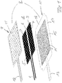
- an electrode 1 is formed by two partial electrodes 2, 3, which are not connected to one another and are at a defined distance from one another.
- the partial electrodes 2, 3 each consist of a narrow flat supply line 4, which merges into a flat structure 5.
- the flat structures 5 of the two partial electrodes 2, 3 together form an approximately square electrode surface, with a distance 6 between the flat structures 5 in the longitudinal direction defined by the leads 4 in the exemplary embodiment shown.
- the flat structures 5 of the partial electrodes 3 have a number of through openings 7, the function of which is explained in more detail below.
- the material of the partial electrodes can be a metallic foil, a thin metallic sheet or a plastic layer, in particular a silicone layer, made conductive by the addition of conductive particles.
- the electrode 1 is covered on all sides by a dielectric 8, which in Figure 1 is shown as consisting of an upper dielectric layer 9 and a lower dielectric layer 10.
- the upper dielectric layer 9 extends beyond the common surface of the two partial electrodes 2, 3 with its surface on all sides and is also provided with through openings 11 which are arranged such that they are aligned with the through openings 7 of the partial electrodes 2, 3.
- the upper dielectric layer is solid in order to bring about a reliable electrical insulation between the partial electrodes 2, 3.
- Both the upper dielectric layer 9 and the lower dielectric layer 10 each have an extension 12, 13 with which the leads 4 are shielded from the environment.
- the through openings 11 of the upper dielectric layer 9 are formed concentrically with the through openings 7, but have a smaller diameter, so that a layer of the dielectric also shields the material of the partial electrodes 2, 3 in the region of the through openings 7. Therefore, no direct electrical connection to the partial electrodes 2, 3 can be established even via a liquid.
- the upper dielectric layer 9 can be penetrated by through openings 14.
- the through openings 14 are also formed concentrically with the through openings 7 of the partial electrodes and the through openings 11 of the upper dielectric layer.
- the diameter of the through openings 14 is smaller than the diameter of the through openings 7 of the partial electrodes 2, 3 and the same size as the diameter of the through openings 11 of the upper dielectric layer 9.
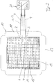
- the lower dielectric layer 10 On the side facing away from the partial electrodes 2, 3, the lower dielectric layer 10 forms a grid structure 15 with intersecting web-like walls, the free edges 16 of which define an abutment side with which an electrode arrangement can rest on a surface to be treated.
- Figure 1 can also be seen that the continuous lower dielectric layer 10 with lateral strips 17, 18 protrudes laterally beyond the contour of the upper dielectric layer 9 and thereby forms approaches with which the electrode arrangement can be attached to the surface to be treated.
- the side strips can be coated on their underside with a pressure sensitive adhesive or formed from an adhesive material.
- Figure 2 shows a plan view of the underside, ie the contact side, according to the electrode arrangement Figure 1 .
- This illustration shows that the lattice structure forms square chambers, in the middle of which are the through openings 14 of the lower dielectric layer, which are arranged concentrically with the (larger) through openings 7 of the partial electrodes 2, 3.
- through-channels 7, 14, which are aligned with one another form continuous channels which are bounded on all sides by the material of dielectric 8 and in particular shield the material of sub-electrodes 2, 3 also in the area of through-holes 7.
- the Figure 2 also reveals that the dielectric material is solid in the area of the distance 6 between the partial electrodes 2, 3.
- the grid structure 15 is reinforced outside the region of the partial electrodes 2, 3 with an edge structure 19 made of small chambers arranged in a frame-like manner.
- the supply lines 4 are contacted in a control device 20 by means of a schematically illustrated contact arrangement.
- the leads 4 can be contacted, for example, by cutting contacts, which cut automatically through the material of the dielectric 8 up to the conductive leads 4 and thereby close an insulating housing.
- Such cutting contacts are commercially available and do not need to be explained in more detail here.
- the supply lines are supplied with alternating high voltages, which are shifted with respect to one another with respect to one another in such a way that, in the ideal case, they compensate for one another.
- Enclosing the partial electrodes 2, 3 with their leads 4 with the material of the dielectric 8 can be carried out in the usual way.
- the upper dielectric layer 9 and the lower dielectric layer 10 are formed such that they are welded to one another as a thermoplastic material or can only be glued to one another.
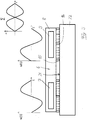
- Figure 3 illustrates schematically that the partial electrodes 2, 3, which are embedded in the dielectric 8 and insulated from one another by the distance 6, in the region of the lattice structure 15, which acts as a spacer, cause the formation of a plasma that is homogeneous in that the the electrical field which triggers the plasma runs homogeneously between the partial electrodes 2, 3 and the surface 21, which is illustrated here by field lines aligned parallel to one another. It also becomes clear that no plasma is formed in the area of the distance 6, because this area is practically field-free. This is due to the fact that the two sub-electrodes 2, 3 are driven with alternating high voltages which are the same in terms of waveform and size, as shown in FIG Figure 3 is shown schematically above the partial electrodes 2, 3.
- the sum curve ⁇ also shown shows that the resulting field in the area of the distance 6 is zero, because the two alternating high voltages ideally cancel each other out to zero. This prevents field phenomena distorting the plasma formation from occurring in the area between the partial electrodes 2, 3. In particular, voltage peaks are avoided.
- the formation of the electrode 1 with two partial electrodes 2, 3 is preferred because it is the easiest to implement. However, for larger surfaces to be treated, it is also conceivable to provide an arrangement with, for example, four partial electrodes, which, for example, form a common square electrode area with four square flat structures 5. The partial electrodes would then be driven diagonally with the same waveforms and adjacent with opposite waveforms.
Landscapes
- Engineering & Computer Science (AREA)
- Physics & Mathematics (AREA)
- Plasma & Fusion (AREA)
- Spectroscopy & Molecular Physics (AREA)
- Health & Medical Sciences (AREA)
- Life Sciences & Earth Sciences (AREA)
- Veterinary Medicine (AREA)
- Radiology & Medical Imaging (AREA)
- Biomedical Technology (AREA)
- Animal Behavior & Ethology (AREA)
- General Health & Medical Sciences (AREA)
- Public Health (AREA)
- Nuclear Medicine, Radiotherapy & Molecular Imaging (AREA)
- Plasma Technology (AREA)
- Treatments Of Macromolecular Shaped Articles (AREA)
- Physical Or Chemical Processes And Apparatus (AREA)
- Electrotherapy Devices (AREA)
- Chemical Vapour Deposition (AREA)
- Treatment Of Fiber Materials (AREA)
Priority Applications (1)
| Application Number | Priority Date | Filing Date | Title |
|---|---|---|---|
| PL18200611T PL3448130T3 (pl) | 2016-09-30 | 2017-07-21 | Układ elektrod do utworzenia dielektrycznie zahamowanego wyładowania plazmowego |
Applications Claiming Priority (3)
| Application Number | Priority Date | Filing Date | Title |
|---|---|---|---|
| DE102016118569.8A DE102016118569A1 (de) | 2016-09-30 | 2016-09-30 | Elektrodenanordnung zur Ausbildung einer dielektrisch behinderten Plasmaentladung |
| PCT/DE2017/100612 WO2018059612A1 (de) | 2016-09-30 | 2017-07-21 | Elektrodenanordnung zur ausbildung einer dielektrisch behinderten plasmaentladung |
| EP17754249.5A EP3320759B1 (de) | 2016-09-30 | 2017-07-21 | Elektrodenanordnung zur ausbildung einer dielektrisch behinderten plasmaentladung |
Related Parent Applications (2)
| Application Number | Title | Priority Date | Filing Date |
|---|---|---|---|
| EP17754249.5A Division EP3320759B1 (de) | 2016-09-30 | 2017-07-21 | Elektrodenanordnung zur ausbildung einer dielektrisch behinderten plasmaentladung |
| EP17754249.5A Division-Into EP3320759B1 (de) | 2016-09-30 | 2017-07-21 | Elektrodenanordnung zur ausbildung einer dielektrisch behinderten plasmaentladung |
Publications (2)
| Publication Number | Publication Date |
|---|---|
| EP3448130A1 EP3448130A1 (de) | 2019-02-27 |
| EP3448130B1 true EP3448130B1 (de) | 2020-04-08 |
Family
ID=59655806
Family Applications (2)
| Application Number | Title | Priority Date | Filing Date |
|---|---|---|---|
| EP18200611.4A Active EP3448130B1 (de) | 2016-09-30 | 2017-07-21 | Elektrodenanordnung zur ausbildung einer dielektrisch behinderten plasmaentladung |
| EP17754249.5A Active EP3320759B1 (de) | 2016-09-30 | 2017-07-21 | Elektrodenanordnung zur ausbildung einer dielektrisch behinderten plasmaentladung |
Family Applications After (1)
| Application Number | Title | Priority Date | Filing Date |
|---|---|---|---|
| EP17754249.5A Active EP3320759B1 (de) | 2016-09-30 | 2017-07-21 | Elektrodenanordnung zur ausbildung einer dielektrisch behinderten plasmaentladung |
Country Status (14)
| Country | Link |
|---|---|
| US (1) | US11785700B2 (https=) |
| EP (2) | EP3448130B1 (https=) |
| JP (1) | JP7074351B2 (https=) |
| KR (1) | KR102460970B1 (https=) |
| CN (1) | CN109792832B (https=) |
| BR (1) | BR112019001274B1 (https=) |
| DE (1) | DE102016118569A1 (https=) |
| DK (1) | DK3448130T3 (https=) |
| ES (2) | ES2710316T3 (https=) |
| MX (1) | MX386548B (https=) |
| PL (1) | PL3448130T3 (https=) |
| RU (1) | RU2737280C2 (https=) |
| TR (1) | TR201901068T4 (https=) |
| WO (1) | WO2018059612A1 (https=) |
Families Citing this family (12)
| Publication number | Priority date | Publication date | Assignee | Title |
|---|---|---|---|---|
| DE102016118569A1 (de) * | 2016-09-30 | 2018-04-05 | Cinogy Gmbh | Elektrodenanordnung zur Ausbildung einer dielektrisch behinderten Plasmaentladung |
| NL2017822B1 (en) * | 2016-11-18 | 2018-05-25 | Plasmacure B V | Non-Thermal Plasma Device with electromagnetic compatibility control |
| DE102017100192A1 (de) * | 2017-01-06 | 2018-07-12 | Cinogy Gmbh | Permanente Wundauflage mit Plasmaelektrode |
| KR101813558B1 (ko) * | 2017-04-12 | 2018-01-03 | 주식회사 서린메디케어 | 프락셔널 플라즈마를 이용한 피부 치료장치 |
| DE102019109940B4 (de) * | 2019-04-15 | 2020-12-10 | Cinogy Gmbh | Behandlungsanordnung für die Behandlung einer Oberfläche eines Körpers mit einem dielektrisch behinderten Plasma |
| NL2027148B1 (en) * | 2020-12-17 | 2022-07-11 | Plasmacure B V | Treatment pad for a dielectric barrier discharge plasma treatment |
| DE102021123900A1 (de) | 2021-09-15 | 2023-03-16 | Cinogy Gmbh | Schuhwerk mit einer Elektrodenanordnung zum Erzeugen von Plasma |
| DE102021124377A1 (de) | 2021-09-21 | 2023-03-23 | Cinogy Gmbh | Elektrodenanordnung für eine Plasmaentladung |
| DE102022105186A1 (de) | 2022-03-04 | 2023-09-07 | Cinogy Gmbh | Wundauflage |
| DE102022124101A1 (de) | 2022-09-20 | 2024-03-21 | Cinogy Gmbh | Plasma-Behandlungsanordnung |
| DE102023104705A1 (de) | 2023-02-27 | 2024-08-29 | Cinogy Gmbh | Plasma-Behandlungsanordnung |
| DE102023104707B3 (de) | 2023-02-27 | 2024-05-02 | Cinogy Gmbh | Plasmabehandlungsanordnung |
Family Cites Families (36)
| Publication number | Priority date | Publication date | Assignee | Title |
|---|---|---|---|---|
| DE19532105C2 (de) * | 1994-08-30 | 2002-11-14 | Fraunhofer Ges Forschung | Verfahren und Vorrichtung zur Behandlung von dreidimensionalen Werkstücken mit einer direkten Barrierenentladung sowie Verfahren zur Herstellung einer mit einer Barriere versehenen Elektrode für diese Barrierenentladung |
| US6146599A (en) * | 1999-02-24 | 2000-11-14 | Seagate Technology Llc | Dielectric barrier discharge system and method for decomposing hazardous compounds in fluids |
| KR20050043740A (ko) * | 2001-11-02 | 2005-05-11 | 플라스마솔 코포레이션 | 저온 플라즈마 슬릿 방전 장치 |
| US7543546B2 (en) * | 2003-05-27 | 2009-06-09 | Matsushita Electric Works, Ltd. | Plasma processing apparatus, method for producing reaction vessel for plasma generation, and plasma processing method |
| JP4603326B2 (ja) * | 2004-09-21 | 2010-12-22 | 積水化学工業株式会社 | 表面処理装置 |
| JP2006302625A (ja) | 2005-04-19 | 2006-11-02 | Matsushita Electric Works Ltd | プラズマ処理装置及びプラズマ処理方法 |
| DE102005029360B4 (de) * | 2005-06-24 | 2011-11-10 | Softal Corona & Plasma Gmbh | Zwei Verfahren zur kontinuierlichen Atmosphärendruck Plasmabehandlung von Werkstücken, insbesondere Materialplatten oder -bahnen |
| SK51082006A3 (sk) * | 2006-12-05 | 2008-07-07 | Fakulta Matematiky, Fyziky A Informatiky Univerzitfakulta Matematiky, Fyziky A Informatiky Univerzity Komensk�Hoy Komensk�Ho | Zariadenie a spôsob úpravy povrchov kovov a metaloZariadenie a spôsob úpravy povrchov kovov a metaloidov, oxidov kovov a oxidov metaloidov a nitridovidov, oxidov kovov a oxidov metaloidov a nitridovkovov a nitridov metaloidovkovov a nitridov metaloidov |
| DE102007030915A1 (de) * | 2007-07-03 | 2009-01-22 | Cinogy Gmbh | Vorrichtung zur Behandlung von Oberflächen mit einem mittels einer Elektrode über ein Feststoff-Dielektrikum durch eine dielektrische behinderte Gasentladung erzeugten Plasma |
| JP5466951B2 (ja) * | 2008-01-18 | 2014-04-09 | 京セラ株式会社 | プラズマ発生体、プラズマ発生体を用いた放電装置および反応装置 |
| WO2009098662A1 (en) | 2008-02-08 | 2009-08-13 | Ecole Polytechnique Federale De Lausanne (Epfl) | Long lifetime system for the generation of surface plasmas |
| EP2205049A1 (en) * | 2008-12-30 | 2010-07-07 | Nederlandse Organisatie voor toegepast-natuurwetenschappelijk Onderzoek TNO | Apparatus and method for treating an object |
| CN102282916A (zh) | 2009-01-13 | 2011-12-14 | 里巴贝鲁株式会社 | 等离子体生成装置及方法 |
| DE102009047220A1 (de) | 2009-11-27 | 2011-06-01 | Leibniz-Institut für Plasmaforschung und Technologie e.V. | Vorrichtung und Verfahren zur Erzeugung eines gepulsten Anisothermen Atmosphärendruck-Plasmas |
| DE102009060627B4 (de) * | 2009-12-24 | 2014-06-05 | Cinogy Gmbh | Elektrodenanordnung für eine dielektrisch behinderte Plasmabehandlung |
| KR101112741B1 (ko) * | 2010-04-20 | 2012-02-22 | 다이나믹솔라디자인 주식회사 | 다중 분할 전극 세트를 위한 급전 장치를 구비한 플라즈마 챔버 |
| DE102010024086A1 (de) * | 2010-06-17 | 2011-12-22 | WPNLB UG (haftungsbeschränkt) & Co. KG | Vorrichtung zur kontinuierlichen Plasmabehandlung und/oder Plasmabeschichtung eines Materialstücks |
| EP2608329A4 (en) * | 2010-08-18 | 2014-10-22 | Kyocera Corp | ION CONVEYOR BODY AND ION WINDER GENERATION DEVICE |
| US8766177B2 (en) * | 2010-10-11 | 2014-07-01 | University Of North Texas | Nanomanipulation coupled nanospray mass spectrometry (NMS) |
| DE102011000261A1 (de) * | 2011-01-21 | 2012-07-26 | Hochschule für angewandte Wissenschaft und Kunst Fachhochschule Hildesheim/Holzminden/Göttingen | Dielektrische Koplanarentladungsquelle für eine Oberflächenbehandlung unter Atmosphärendruck |
| US9387269B2 (en) * | 2011-01-28 | 2016-07-12 | Bovie Medical Corporation | Cold plasma jet hand sanitizer |
| DE102011010273A1 (de) * | 2011-02-02 | 2012-08-02 | Cinogy Gmbh | Verfahren zur Behandlung von menschlichem oder tierischem Haar und Gerät zur Durchführung des Verfahrens |
| DE102011001416A1 (de) | 2011-03-18 | 2012-09-20 | Manfred H. Langner | Plasmabehandlungseinrichtung und Verfahren zum Betreiben der Plasmabehandlungseinrichtung |
| DE102011076806A1 (de) * | 2011-05-31 | 2012-12-06 | Leibniz-Institut für Plasmaforschung und Technologie e.V. | Vorrichtung und Verfahren zur Erzeugung eines kalten, homogenen Plasmas unter Atmosphärendruckbedingungen |
| EP2794078A2 (en) * | 2012-01-20 | 2014-10-29 | University of Newcastle Upon Tyne | Integrated intensified biorefinery for gas-to-liquid conversion |
| US9117616B2 (en) * | 2012-07-13 | 2015-08-25 | Sp Tech Co., Ltd. | Dielectric barrier discharge-type electrode structure for generating plasma having conductive body protrusion on electrodes |
| WO2014119349A1 (ja) | 2013-02-04 | 2014-08-07 | 株式会社クリエイティブ テクノロジー | プラズマ発生装置 |
| RU2526810C1 (ru) * | 2013-02-12 | 2014-08-27 | Федеральное государственное бюджетное образовательное учреждение высшего профессионального образования "Санкт-Петербургский государственный университет" (СПбГУ) | Плазменный дезинфектор для биологических тканей |
| JP6180016B2 (ja) * | 2013-04-23 | 2017-08-16 | 沖野 晃俊 | 大気圧プラズマを用いた生物細胞および外皮系のケア装置 |
| WO2015088948A1 (en) * | 2013-12-09 | 2015-06-18 | EP Technologies LLC | Shape conforming flexible dielectric barrier discharge plasma generators |
| EP3086838A4 (en) * | 2013-12-27 | 2017-08-23 | Moe Medical Devices LLC | Applying electric field treatment to parts of the body |
| DE102014013716B4 (de) * | 2014-09-11 | 2022-04-07 | Cinogy Gmbh | Elektrodenanordnung zur Ausbildung einer dielektrisch behinderten Plasmaentladung |
| JP2016140857A (ja) * | 2015-02-05 | 2016-08-08 | 株式会社東芝 | 気流発生装置 |
| DE102016118569A1 (de) * | 2016-09-30 | 2018-04-05 | Cinogy Gmbh | Elektrodenanordnung zur Ausbildung einer dielektrisch behinderten Plasmaentladung |
| DE102017106570A1 (de) * | 2017-03-28 | 2018-10-04 | Cinogy Gmbh | Flächige flexible Auflageanordnung |
| DE102019101063B4 (de) * | 2019-01-16 | 2021-02-25 | Cinogy Gmbh | Plasma-Behandlungsanordnung und Verfahren zur Anpassung der Größe einer Auflagefläche der Plasma-Behandlungsanordnung an die Größe der zu behandelnden Oberfläche |
-
2016
- 2016-09-30 DE DE102016118569.8A patent/DE102016118569A1/de not_active Withdrawn
-
2017
- 2017-07-21 MX MX2019000934A patent/MX386548B/es unknown
- 2017-07-21 PL PL18200611T patent/PL3448130T3/pl unknown
- 2017-07-21 BR BR112019001274-5A patent/BR112019001274B1/pt not_active IP Right Cessation
- 2017-07-21 JP JP2019505236A patent/JP7074351B2/ja active Active
- 2017-07-21 ES ES17754249T patent/ES2710316T3/es active Active
- 2017-07-21 ES ES18200611T patent/ES2797948T3/es active Active
- 2017-07-21 TR TR2019/01068T patent/TR201901068T4/tr unknown
- 2017-07-21 US US16/329,455 patent/US11785700B2/en active Active
- 2017-07-21 CN CN201780051231.7A patent/CN109792832B/zh active Active
- 2017-07-21 DK DK18200611.4T patent/DK3448130T3/da active
- 2017-07-21 RU RU2019103085A patent/RU2737280C2/ru active
- 2017-07-21 KR KR1020197011055A patent/KR102460970B1/ko active Active
- 2017-07-21 EP EP18200611.4A patent/EP3448130B1/de active Active
- 2017-07-21 WO PCT/DE2017/100612 patent/WO2018059612A1/de not_active Ceased
- 2017-07-21 EP EP17754249.5A patent/EP3320759B1/de active Active
Non-Patent Citations (1)
| Title |
|---|
| None * |
Also Published As
| Publication number | Publication date |
|---|---|
| MX386548B (es) | 2025-03-19 |
| ES2710316T3 (es) | 2019-04-24 |
| BR112019001274B1 (pt) | 2023-03-14 |
| RU2019103085A3 (https=) | 2020-10-30 |
| EP3448130A1 (de) | 2019-02-27 |
| EP3320759B1 (de) | 2019-01-02 |
| ES2797948T3 (es) | 2020-12-04 |
| US11785700B2 (en) | 2023-10-10 |
| JP7074351B2 (ja) | 2022-05-24 |
| RU2737280C2 (ru) | 2020-11-26 |
| EP3320759A1 (de) | 2018-05-16 |
| BR112019001274A2 (pt) | 2019-04-30 |
| TR201901068T4 (tr) | 2019-02-21 |
| US20190223280A1 (en) | 2019-07-18 |
| CN109792832A (zh) | 2019-05-21 |
| WO2018059612A1 (de) | 2018-04-05 |
| DK3448130T3 (da) | 2020-06-29 |
| JP2019530948A (ja) | 2019-10-24 |
| DE102016118569A1 (de) | 2018-04-05 |
| KR102460970B1 (ko) | 2022-10-31 |
| RU2019103085A (ru) | 2020-10-30 |
| CN109792832B (zh) | 2025-08-12 |
| PL3448130T3 (pl) | 2020-10-19 |
| KR20190055165A (ko) | 2019-05-22 |
| MX2019000934A (es) | 2019-07-04 |
Similar Documents
| Publication | Publication Date | Title |
|---|---|---|
| EP3448130B1 (de) | Elektrodenanordnung zur ausbildung einer dielektrisch behinderten plasmaentladung | |
| EP3566552B1 (de) | Flächiges flexibles auflagestück für eine dielektrisch behinderte plasmabehandlung | |
| DE102009060627B4 (de) | Elektrodenanordnung für eine dielektrisch behinderte Plasmabehandlung | |
| DE102016108450B4 (de) | Behandlungsanordnung und Verfahren zur Herstellung einer Behandlungsanordnung | |
| DE102014013716B4 (de) | Elektrodenanordnung zur Ausbildung einer dielektrisch behinderten Plasmaentladung | |
| EP2163143B1 (de) | Vorrichtung zur behandlung von oberflächen mit einem mittels einer elektrode über ein feststoff-dielektrikum durch eine dielektrisch behinderte gasentladung erzeugten plasma | |
| WO2012175066A1 (de) | Elektrodenanordnung für eine dielektrisch behinderte gasentladung | |
| EP3171676A1 (de) | Plasmaerzeugungsvorrichtung, plasmaerzeugungssystem und verfahren zur erzeugung von plasma | |
| EP1106033A1 (de) | Widerstandsflächen-heizelement | |
| EP3630279B1 (de) | Flächige auflageanordnung ausgebildet zur erzeugung eines dielektrisch behinderten plasmas | |
| EP3592421A1 (de) | Flächige flexible elektrodenanordnung für eine dielektrisch behinderte plasmaentladung | |
| DE102018126492A1 (de) | Plasma-Behandlungsgerät | |
| DE202018106346U1 (de) | Plasma-Behandlungsgerät | |
| EP3066700A1 (de) | Piezoelektrischer transformator und gegenelektrode | |
| DE102008006256B4 (de) | Baugruppe zur Erzeugung von Ozon | |
| WO2023046726A1 (de) | Elektrodenanordnung für eine plasmaentladung | |
| WO2000003466A1 (de) | Vorrichtung zur erzeugung ionisierter gase mittels korona-entladungen | |
| DE29911754U1 (de) | Vorrichtung zur Erzeugung ionisierter Gase mittels Korona-Entladungen | |
| DE1232649B (de) | Vorrichtung zum Erzeugen einer Aneinanderhaftung zwischen Festkoerpern |
Legal Events
| Date | Code | Title | Description |
|---|---|---|---|
| PUAI | Public reference made under article 153(3) epc to a published international application that has entered the european phase |
Free format text: ORIGINAL CODE: 0009012 |
|
| STAA | Information on the status of an ep patent application or granted ep patent |
Free format text: STATUS: THE APPLICATION HAS BEEN PUBLISHED |
|
| AC | Divisional application: reference to earlier application |
Ref document number: 3320759 Country of ref document: EP Kind code of ref document: P |
|
| AK | Designated contracting states |
Kind code of ref document: A1 Designated state(s): AL AT BE BG CH CY CZ DE DK EE ES FI FR GB GR HR HU IE IS IT LI LT LU LV MC MK MT NL NO PL PT RO RS SE SI SK SM TR |
|
| AX | Request for extension of the european patent |
Extension state: BA ME |
|
| STAA | Information on the status of an ep patent application or granted ep patent |
Free format text: STATUS: REQUEST FOR EXAMINATION WAS MADE |
|
| 17P | Request for examination filed |
Effective date: 20190730 |
|
| RBV | Designated contracting states (corrected) |
Designated state(s): AL AT BE BG CH CY CZ DE DK EE ES FI FR GB GR HR HU IE IS IT LI LT LU LV MC MK MT NL NO PL PT RO RS SE SI SK SM TR |
|
| GRAJ | Information related to disapproval of communication of intention to grant by the applicant or resumption of examination proceedings by the epo deleted |
Free format text: ORIGINAL CODE: EPIDOSDIGR1 |
|
| STAA | Information on the status of an ep patent application or granted ep patent |
Free format text: STATUS: GRANT OF PATENT IS INTENDED |
|
| GRAP | Despatch of communication of intention to grant a patent |
Free format text: ORIGINAL CODE: EPIDOSNIGR1 |
|
| RIC1 | Information provided on ipc code assigned before grant |
Ipc: H05H 1/24 20060101AFI20191030BHEP |
|
| INTG | Intention to grant announced |
Effective date: 20191112 |
|
| GRAS | Grant fee paid |
Free format text: ORIGINAL CODE: EPIDOSNIGR3 |
|
| GRAA | (expected) grant |
Free format text: ORIGINAL CODE: 0009210 |
|
| STAA | Information on the status of an ep patent application or granted ep patent |
Free format text: STATUS: THE PATENT HAS BEEN GRANTED |
|
| AC | Divisional application: reference to earlier application |
Ref document number: 3320759 Country of ref document: EP Kind code of ref document: P |
|
| AK | Designated contracting states |
Kind code of ref document: B1 Designated state(s): AL AT BE BG CH CY CZ DE DK EE ES FI FR GB GR HR HU IE IS IT LI LT LU LV MC MK MT NL NO PL PT RO RS SE SI SK SM TR |
|
| REG | Reference to a national code |
Ref country code: AT Ref legal event code: REF Ref document number: 1256164 Country of ref document: AT Kind code of ref document: T Effective date: 20200415 Ref country code: CH Ref legal event code: EP |
|
| REG | Reference to a national code |
Ref country code: DE Ref legal event code: R096 Ref document number: 502017004691 Country of ref document: DE |
|
| REG | Reference to a national code |
Ref country code: IE Ref legal event code: FG4D Free format text: LANGUAGE OF EP DOCUMENT: GERMAN |
|
| REG | Reference to a national code |
Ref country code: DK Ref legal event code: T3 Effective date: 20200625 |
|
| REG | Reference to a national code |
Ref country code: CH Ref legal event code: NV Representative=s name: BRAUNPAT BRAUN EDER AG, CH |
|
| REG | Reference to a national code |
Ref country code: SE Ref legal event code: TRGR |
|
| REG | Reference to a national code |
Ref country code: NL Ref legal event code: FP |
|
| REG | Reference to a national code |
Ref country code: LT Ref legal event code: MG4D |
|
| PG25 | Lapsed in a contracting state [announced via postgrant information from national office to epo] |
Ref country code: LT Free format text: LAPSE BECAUSE OF FAILURE TO SUBMIT A TRANSLATION OF THE DESCRIPTION OR TO PAY THE FEE WITHIN THE PRESCRIBED TIME-LIMIT Effective date: 20200408 Ref country code: GR Free format text: LAPSE BECAUSE OF FAILURE TO SUBMIT A TRANSLATION OF THE DESCRIPTION OR TO PAY THE FEE WITHIN THE PRESCRIBED TIME-LIMIT Effective date: 20200709 Ref country code: PT Free format text: LAPSE BECAUSE OF FAILURE TO SUBMIT A TRANSLATION OF THE DESCRIPTION OR TO PAY THE FEE WITHIN THE PRESCRIBED TIME-LIMIT Effective date: 20200817 Ref country code: NO Free format text: LAPSE BECAUSE OF FAILURE TO SUBMIT A TRANSLATION OF THE DESCRIPTION OR TO PAY THE FEE WITHIN THE PRESCRIBED TIME-LIMIT Effective date: 20200708 Ref country code: FI Free format text: LAPSE BECAUSE OF FAILURE TO SUBMIT A TRANSLATION OF THE DESCRIPTION OR TO PAY THE FEE WITHIN THE PRESCRIBED TIME-LIMIT Effective date: 20200408 Ref country code: IS Free format text: LAPSE BECAUSE OF FAILURE TO SUBMIT A TRANSLATION OF THE DESCRIPTION OR TO PAY THE FEE WITHIN THE PRESCRIBED TIME-LIMIT Effective date: 20200808 |
|
| PG25 | Lapsed in a contracting state [announced via postgrant information from national office to epo] |
Ref country code: HR Free format text: LAPSE BECAUSE OF FAILURE TO SUBMIT A TRANSLATION OF THE DESCRIPTION OR TO PAY THE FEE WITHIN THE PRESCRIBED TIME-LIMIT Effective date: 20200408 Ref country code: RS Free format text: LAPSE BECAUSE OF FAILURE TO SUBMIT A TRANSLATION OF THE DESCRIPTION OR TO PAY THE FEE WITHIN THE PRESCRIBED TIME-LIMIT Effective date: 20200408 Ref country code: BG Free format text: LAPSE BECAUSE OF FAILURE TO SUBMIT A TRANSLATION OF THE DESCRIPTION OR TO PAY THE FEE WITHIN THE PRESCRIBED TIME-LIMIT Effective date: 20200708 Ref country code: LV Free format text: LAPSE BECAUSE OF FAILURE TO SUBMIT A TRANSLATION OF THE DESCRIPTION OR TO PAY THE FEE WITHIN THE PRESCRIBED TIME-LIMIT Effective date: 20200408 |
|
| REG | Reference to a national code |
Ref country code: ES Ref legal event code: FG2A Ref document number: 2797948 Country of ref document: ES Kind code of ref document: T3 Effective date: 20201204 |
|
| PG25 | Lapsed in a contracting state [announced via postgrant information from national office to epo] |
Ref country code: AL Free format text: LAPSE BECAUSE OF FAILURE TO SUBMIT A TRANSLATION OF THE DESCRIPTION OR TO PAY THE FEE WITHIN THE PRESCRIBED TIME-LIMIT Effective date: 20200408 |
|
| REG | Reference to a national code |
Ref country code: DE Ref legal event code: R097 Ref document number: 502017004691 Country of ref document: DE |
|
| PG25 | Lapsed in a contracting state [announced via postgrant information from national office to epo] |
Ref country code: CZ Free format text: LAPSE BECAUSE OF FAILURE TO SUBMIT A TRANSLATION OF THE DESCRIPTION OR TO PAY THE FEE WITHIN THE PRESCRIBED TIME-LIMIT Effective date: 20200408 Ref country code: SM Free format text: LAPSE BECAUSE OF FAILURE TO SUBMIT A TRANSLATION OF THE DESCRIPTION OR TO PAY THE FEE WITHIN THE PRESCRIBED TIME-LIMIT Effective date: 20200408 Ref country code: EE Free format text: LAPSE BECAUSE OF FAILURE TO SUBMIT A TRANSLATION OF THE DESCRIPTION OR TO PAY THE FEE WITHIN THE PRESCRIBED TIME-LIMIT Effective date: 20200408 Ref country code: RO Free format text: LAPSE BECAUSE OF FAILURE TO SUBMIT A TRANSLATION OF THE DESCRIPTION OR TO PAY THE FEE WITHIN THE PRESCRIBED TIME-LIMIT Effective date: 20200408 |
|
| PLBE | No opposition filed within time limit |
Free format text: ORIGINAL CODE: 0009261 |
|
| STAA | Information on the status of an ep patent application or granted ep patent |
Free format text: STATUS: NO OPPOSITION FILED WITHIN TIME LIMIT |
|
| PG25 | Lapsed in a contracting state [announced via postgrant information from national office to epo] |
Ref country code: MC Free format text: LAPSE BECAUSE OF FAILURE TO SUBMIT A TRANSLATION OF THE DESCRIPTION OR TO PAY THE FEE WITHIN THE PRESCRIBED TIME-LIMIT Effective date: 20200408 Ref country code: SK Free format text: LAPSE BECAUSE OF FAILURE TO SUBMIT A TRANSLATION OF THE DESCRIPTION OR TO PAY THE FEE WITHIN THE PRESCRIBED TIME-LIMIT Effective date: 20200408 |
|
| 26N | No opposition filed |
Effective date: 20210112 |
|
| REG | Reference to a national code |
Ref country code: BE Ref legal event code: MM Effective date: 20200731 |
|
| PG25 | Lapsed in a contracting state [announced via postgrant information from national office to epo] |
Ref country code: LU Free format text: LAPSE BECAUSE OF NON-PAYMENT OF DUE FEES Effective date: 20200721 |
|
| PG25 | Lapsed in a contracting state [announced via postgrant information from national office to epo] |
Ref country code: BE Free format text: LAPSE BECAUSE OF NON-PAYMENT OF DUE FEES Effective date: 20200731 Ref country code: SI Free format text: LAPSE BECAUSE OF FAILURE TO SUBMIT A TRANSLATION OF THE DESCRIPTION OR TO PAY THE FEE WITHIN THE PRESCRIBED TIME-LIMIT Effective date: 20200408 |
|
| PG25 | Lapsed in a contracting state [announced via postgrant information from national office to epo] |
Ref country code: IE Free format text: LAPSE BECAUSE OF NON-PAYMENT OF DUE FEES Effective date: 20200721 |
|
| PG25 | Lapsed in a contracting state [announced via postgrant information from national office to epo] |
Ref country code: MT Free format text: LAPSE BECAUSE OF FAILURE TO SUBMIT A TRANSLATION OF THE DESCRIPTION OR TO PAY THE FEE WITHIN THE PRESCRIBED TIME-LIMIT Effective date: 20200408 Ref country code: CY Free format text: LAPSE BECAUSE OF FAILURE TO SUBMIT A TRANSLATION OF THE DESCRIPTION OR TO PAY THE FEE WITHIN THE PRESCRIBED TIME-LIMIT Effective date: 20200408 |
|
| PG25 | Lapsed in a contracting state [announced via postgrant information from national office to epo] |
Ref country code: MK Free format text: LAPSE BECAUSE OF FAILURE TO SUBMIT A TRANSLATION OF THE DESCRIPTION OR TO PAY THE FEE WITHIN THE PRESCRIBED TIME-LIMIT Effective date: 20200408 |
|
| P01 | Opt-out of the competence of the unified patent court (upc) registered |
Effective date: 20230526 |
|
| REG | Reference to a national code |
Ref country code: AT Ref legal event code: MM01 Ref document number: 1256164 Country of ref document: AT Kind code of ref document: T Effective date: 20220721 |
|
| PG25 | Lapsed in a contracting state [announced via postgrant information from national office to epo] |
Ref country code: AT Free format text: LAPSE BECAUSE OF NON-PAYMENT OF DUE FEES Effective date: 20220721 |
|
| PGFP | Annual fee paid to national office [announced via postgrant information from national office to epo] |
Ref country code: PL Payment date: 20230710 Year of fee payment: 7 |
|
| PGFP | Annual fee paid to national office [announced via postgrant information from national office to epo] |
Ref country code: NL Payment date: 20250723 Year of fee payment: 9 |
|
| PGFP | Annual fee paid to national office [announced via postgrant information from national office to epo] |
Ref country code: ES Payment date: 20250819 Year of fee payment: 9 |
|
| PGFP | Annual fee paid to national office [announced via postgrant information from national office to epo] |
Ref country code: DK Payment date: 20250723 Year of fee payment: 9 Ref country code: DE Payment date: 20250709 Year of fee payment: 9 |
|
| PGFP | Annual fee paid to national office [announced via postgrant information from national office to epo] |
Ref country code: TR Payment date: 20250717 Year of fee payment: 9 Ref country code: IT Payment date: 20250731 Year of fee payment: 9 |
|
| PGFP | Annual fee paid to national office [announced via postgrant information from national office to epo] |
Ref country code: GB Payment date: 20250724 Year of fee payment: 9 |
|
| PGFP | Annual fee paid to national office [announced via postgrant information from national office to epo] |
Ref country code: FR Payment date: 20250723 Year of fee payment: 9 |
|
| PGFP | Annual fee paid to national office [announced via postgrant information from national office to epo] |
Ref country code: SE Payment date: 20250723 Year of fee payment: 9 Ref country code: CH Payment date: 20250801 Year of fee payment: 9 |