EP3448130B1 - Electrode assembly for forming a dielectrically impeded plasma discharge - Google Patents
Electrode assembly for forming a dielectrically impeded plasma discharge Download PDFInfo
- Publication number
- EP3448130B1 EP3448130B1 EP18200611.4A EP18200611A EP3448130B1 EP 3448130 B1 EP3448130 B1 EP 3448130B1 EP 18200611 A EP18200611 A EP 18200611A EP 3448130 B1 EP3448130 B1 EP 3448130B1
- Authority
- EP
- European Patent Office
- Prior art keywords
- electrode
- dielectric
- partial electrodes
- electrode arrangement
- treated
- Prior art date
- Legal status (The legal status is an assumption and is not a legal conclusion. Google has not performed a legal analysis and makes no representation as to the accuracy of the status listed.)
- Active
Links
- 230000005284 excitation Effects 0.000 claims description 3
- 238000000034 method Methods 0.000 claims description 3
- 230000010355 oscillation Effects 0.000 claims description 3
- 230000001960 triggered effect Effects 0.000 claims description 2
- 230000004888 barrier function Effects 0.000 claims 1
- 230000015572 biosynthetic process Effects 0.000 description 10
- 239000000463 material Substances 0.000 description 9
- 238000000926 separation method Methods 0.000 description 8
- 206010052428 Wound Diseases 0.000 description 7
- 208000027418 Wounds and injury Diseases 0.000 description 7
- 230000005684 electric field Effects 0.000 description 4
- 229920001296 polysiloxane Polymers 0.000 description 4
- 239000004033 plastic Substances 0.000 description 3
- 238000013459 approach Methods 0.000 description 2
- 239000004020 conductor Substances 0.000 description 2
- 239000007788 liquid Substances 0.000 description 2
- 239000002245 particle Substances 0.000 description 2
- 238000009832 plasma treatment Methods 0.000 description 2
- 239000007787 solid Substances 0.000 description 2
- 230000029663 wound healing Effects 0.000 description 2
- OKTJSMMVPCPJKN-UHFFFAOYSA-N Carbon Chemical compound [C] OKTJSMMVPCPJKN-UHFFFAOYSA-N 0.000 description 1
- CBENFWSGALASAD-UHFFFAOYSA-N Ozone Chemical compound [O-][O+]=O CBENFWSGALASAD-UHFFFAOYSA-N 0.000 description 1
- 239000004820 Pressure-sensitive adhesive Substances 0.000 description 1
- 230000006978 adaptation Effects 0.000 description 1
- 239000000853 adhesive Substances 0.000 description 1
- 230000001070 adhesive effect Effects 0.000 description 1
- 230000009286 beneficial effect Effects 0.000 description 1
- 229910052799 carbon Inorganic materials 0.000 description 1
- 239000002482 conductive additive Substances 0.000 description 1
- 238000010276 construction Methods 0.000 description 1
- 239000000645 desinfectant Substances 0.000 description 1
- 239000003989 dielectric material Substances 0.000 description 1
- 238000010292 electrical insulation Methods 0.000 description 1
- 238000005516 engineering process Methods 0.000 description 1
- 239000012530 fluid Substances 0.000 description 1
- 239000011888 foil Substances 0.000 description 1
- 230000001788 irregular Effects 0.000 description 1
- 239000007769 metal material Substances 0.000 description 1
- 239000002923 metal particle Substances 0.000 description 1
- 230000037384 skin absorption Effects 0.000 description 1
- 231100000274 skin absorption Toxicity 0.000 description 1
- 125000006850 spacer group Chemical group 0.000 description 1
- 238000004659 sterilization and disinfection Methods 0.000 description 1
- 239000000126 substance Substances 0.000 description 1
- 239000012815 thermoplastic material Substances 0.000 description 1
Images
Classifications
-
- H—ELECTRICITY
- H05—ELECTRIC TECHNIQUES NOT OTHERWISE PROVIDED FOR
- H05H—PLASMA TECHNIQUE; PRODUCTION OF ACCELERATED ELECTRICALLY-CHARGED PARTICLES OR OF NEUTRONS; PRODUCTION OR ACCELERATION OF NEUTRAL MOLECULAR OR ATOMIC BEAMS
- H05H1/00—Generating plasma; Handling plasma
- H05H1/24—Generating plasma
- H05H1/2406—Generating plasma using dielectric barrier discharges, i.e. with a dielectric interposed between the electrodes
-
- A—HUMAN NECESSITIES
- A61—MEDICAL OR VETERINARY SCIENCE; HYGIENE
- A61N—ELECTROTHERAPY; MAGNETOTHERAPY; RADIATION THERAPY; ULTRASOUND THERAPY
- A61N1/00—Electrotherapy; Circuits therefor
- A61N1/02—Details
- A61N1/04—Electrodes
- A61N1/0404—Electrodes for external use
- A61N1/0408—Use-related aspects
- A61N1/0468—Specially adapted for promoting wound healing
-
- A—HUMAN NECESSITIES
- A61—MEDICAL OR VETERINARY SCIENCE; HYGIENE
- A61N—ELECTROTHERAPY; MAGNETOTHERAPY; RADIATION THERAPY; ULTRASOUND THERAPY
- A61N1/00—Electrotherapy; Circuits therefor
- A61N1/44—Applying ionised fluids
-
- H—ELECTRICITY
- H05—ELECTRIC TECHNIQUES NOT OTHERWISE PROVIDED FOR
- H05H—PLASMA TECHNIQUE; PRODUCTION OF ACCELERATED ELECTRICALLY-CHARGED PARTICLES OR OF NEUTRONS; PRODUCTION OR ACCELERATION OF NEUTRAL MOLECULAR OR ATOMIC BEAMS
- H05H1/00—Generating plasma; Handling plasma
- H05H1/24—Generating plasma
- H05H1/2406—Generating plasma using dielectric barrier discharges, i.e. with a dielectric interposed between the electrodes
- H05H1/2418—Generating plasma using dielectric barrier discharges, i.e. with a dielectric interposed between the electrodes the electrodes being embedded in the dielectric
-
- H—ELECTRICITY
- H05—ELECTRIC TECHNIQUES NOT OTHERWISE PROVIDED FOR
- H05H—PLASMA TECHNIQUE; PRODUCTION OF ACCELERATED ELECTRICALLY-CHARGED PARTICLES OR OF NEUTRONS; PRODUCTION OR ACCELERATION OF NEUTRAL MOLECULAR OR ATOMIC BEAMS
- H05H2245/00—Applications of plasma devices
- H05H2245/30—Medical applications
- H05H2245/34—Skin treatments, e.g. disinfection or wound treatment
-
- H—ELECTRICITY
- H05—ELECTRIC TECHNIQUES NOT OTHERWISE PROVIDED FOR
- H05H—PLASMA TECHNIQUE; PRODUCTION OF ACCELERATED ELECTRICALLY-CHARGED PARTICLES OR OF NEUTRONS; PRODUCTION OR ACCELERATION OF NEUTRAL MOLECULAR OR ATOMIC BEAMS
- H05H2245/00—Applications of plasma devices
- H05H2245/30—Medical applications
- H05H2245/36—Sterilisation of objects, liquids, volumes or surfaces
Definitions
- the invention relates to an electrode arrangement for forming a dielectric disabled plasma discharge between an electrode fed by a control device with an alternating high voltage and a surface of an electrically conductive body to be treated, which serves as a ground electrode, a dielectric completely covering the electrode towards the surface to be treated and one Forms contact side for the surface, the electrode consisting of at least two sub-electrodes arranged at the same distance from the contact side and insulated from one another by the dielectric.
- a flat electrode arrangement which can be flexible, is characterized by the DE 10 2009 060 627 B4 known.
- the flat electrode is embedded between a dielectric underside and a dielectric top, each of which extends in the area beyond the electrode and thus also covers the narrow edge of the electrode, so that contact with the electrode carrying the high voltage is excluded. Also excluded is such an approach to the electrode that a spark could jump over. Rather, the dielectric prevents galvanic current flow from the electrode to the surface to be treated, which serves as a ground electrode.
- the electrode arrangement thus does not have its own ground electrode.
- the underside of the electrode arrangement which faces the surface to be treated, can be formed with protruding knobs with its top on the surface of a surface to be treated rest on the surface to be treated and have continuous spaces in which the plasma can form when an alternating high voltage is applied to the electrode.
- Such an electrode arrangement can be placed on the surface to be treated, the surface to be treated being in particular on the skin of a human or animal body.
- the plasma treatment leads here to pore-deep disinfection of the skin and improves the skin's absorption capacity for nourishing substances that are applied to the treated skin.
- the DE 10 2011 01 416 A1 discloses a flat flexible wound treatment device in which two surface electrodes are formed by interwoven, insulated electrical conductors.
- the high voltage that forms a plasma in the air gaps forms between the conductors. For this it is necessary that the entire electrode arrangement is gas-permeable.
- Electrode arrangements are also known with which a dielectrically impeded surface plasma can be produced.
- WO 2009/098662 A1 describes such an arrangement in which a first flat electrode and a second grid-like electrode are embedded in a dielectric at a distance from one another in the vertical direction of the electrode arrangement, so that an electrical field suitable for forming a plasma is formed on the dielectric surface, which is arranged near the grid-like electrode is.
- An alternating high voltage is applied to the grid-like electrode, while the flat electrode located underneath is connected to ground potential.
- Such an arrangement has a high energy requirement and a low efficiency with regard to the formation of the surface plasma.
- EP 2 953 431 A1 discloses a plasma generator in which partial electrodes are arranged next to one another at the same distance from the surface to be treated and are each connected to one of the two connections of an alternating high-voltage source. This creates an alternating field between the two flat electrodes, one of which forms a common reference electrode of the alternating voltage source. Accordingly, the two electrodes form the starting surfaces for the field lines of the plasma field, so that the plasma field is not directed between the electrodes and the surface to be treated. This arrangement also ensures only a low efficiency due to the formation of a surface plasma.
- electrode arrangements are advantageous, the electrode of which is designed in such a way that a largely homogeneous field profile results between the flat electrode and the surface to be treated as a ground electrode, which leads to a defined and ideally uniform plasma.
- an electrode arrangement of the type mentioned at the outset is characterized in that adjacent sub-electrodes are supplied by the control device with compensating partial alternating high voltages which are mutually equal with respect to the waveform and the voltage level, the alternating high voltages each consisting of a high-frequency oscillation process triggered by an excitation pulse result.
- the electrode arrangement according to the invention is thus based on the known principle of using the surface of the electrically conductive body to be treated as a ground electrode, so that in principle only one electrode is required for the formation of a plasma field, which electrode cooperates with the surface to be treated as a ground electrode for the formation of the plasma .
- an ideally homogeneous electric field largely arises over the surface of the electrode, in which the field lines thus run parallel to one another. Only known at the edge of the electrode can be curved or oblique field lines arise.
- the partial electrodes are preferably of such an area size that the expansion of the electric field and ideally parallel field lines is more than 50%, preferably more than 65% and more preferably more than 80% of the area of the partial electrode.
- the electrodes according to the invention are extended in area and positioned parallel to the contact side of the dielectric.
- the alternating high voltages preferably oscillate around the ground potential. Because of the capacitances and inductivities present in the control device, resonant circuit arrangements are present with which an excitation pulse triggers a high-frequency oscillation process.
- a homogeneous plasma would ideally form in the region of the homogeneous field between the relevant partial electrode and the surface to be treated.
- the voltages would add up and lead to undesired voltage peaks which would disturb the uniform plasma field.
- considerable potential differences would form within the electrically conductive body on the surface to be treated, which could lead to undesired current flows within the body. This can lead to unpleasant and possibly dangerous phenomena on a living body.
- the partial electrodes located next to one another are driven with alternating high voltages, so that an essentially field-free separation region is created in the edge regions of the partial electrodes which lie between the adjacent partial electrodes. Since this separation area can be narrow and linear, the disinfectant products formed in the plasma, for example the OH radicals and ozone molecules which form in the air in the plasma, also become effective in the separation area, since they also reach the range of within their very short life Can reach surfaces in the separation area.
- the electrode arrangement according to the invention with its at least two partial electrodes is therefore designed such that the partial electrodes ideally form a substantially homogeneous field over their almost entire surface with the surface to be treated - and thus ideally a uniform plasma - and a narrow field-free one in principle towards the neighboring partial electrode Let separation area arise. For two adjacent sub-electrodes, one sub-electrode is therefore driven with a positive half-wave of the alternating high voltage, while the other sub-electrode is driven with a negative half-wave, so that the two voltages are compensated for in the separation region.
- the respective half-waves are identical in size and shape, so that a constant center potential that does not change over the period of the alternating high voltage, which corresponds to the ground potential of the ground electrode, is established in the separation region.
- identity of the opposite half-waves can only be approximate, so that there is a constant total potential in the separation region even if there is still a slight fluctuation in the total potential, which is less than five percent of the peak voltage, for example.
- the ideally uniform plasma can in practice be overlaid or disturbed by slight filament discharges, even if the aim is to avoid such filament discharges.
- the peak voltage of the alternating high voltages used can advantageously be between ⁇ 10 kV and ⁇ 100 kV.
- the alternating frequencies of the alternating high voltages are expediently between a few 100 Hz and approximately 100 MHz.
- the partial electrodes and the dielectric are flexible.
- the entire electrode arrangement can follow an irregular surface, so that it can ideally be treated with a uniform plasma field.
- the contact side of the dielectric which faces the surface to be treated, can have a structure, preferably in the form of a grid or nubs, between which the plasma can form, if the dielectric lies with the top of the knobs or other protruding structures on the surface to be treated.
- the electrode arrangement according to the invention can also be designed as a wound dressing if the dielectric is formed from a wound-compatible material, for example suitable silicones, or a layer of a wound-compatible material, for example gauze, is placed on the contact side of the dielectric.
- a wound-compatible material for example suitable silicones
- a layer of a wound-compatible material for example gauze
- the electrode arrangement according to the invention is also suitable for the drainage of wound fluid or for the supply of a wound-healing or wound-healing-promoting liquid if the dielectric and the partial electrodes have passage openings which extend through the electrode arrangements in a vertical direction and are continuously delimited by the dielectric surrounding the partial electrodes .
- the electrode arrangement according to the invention preferably has a high symmetry with respect to the partial electrodes.
- the partial electrodes have the same size, so that the area effective for the formation of the plasma is distributed uniformly over the number of partial electrodes.
- the partial electrodes can consist of a flat metallic material, which is preferably covered on both sides by a dielectric.
- a conductive plastic which can also be positively connected to the dielectric which is likewise formed by a plastic, for example silicone.
- the electrode can, for example, consist of a silicone with conductive additives, in the form of metal particles, carbon particles or the like.
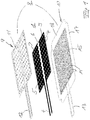
- an electrode 1 is formed by two partial electrodes 2, 3, which are not connected to one another and are at a defined distance from one another.
- the partial electrodes 2, 3 each consist of a narrow flat supply line 4, which merges into a flat structure 5.
- the flat structures 5 of the two partial electrodes 2, 3 together form an approximately square electrode surface, with a distance 6 between the flat structures 5 in the longitudinal direction defined by the leads 4 in the exemplary embodiment shown.
- the flat structures 5 of the partial electrodes 3 have a number of through openings 7, the function of which is explained in more detail below.
- the material of the partial electrodes can be a metallic foil, a thin metallic sheet or a plastic layer, in particular a silicone layer, made conductive by the addition of conductive particles.
- the electrode 1 is covered on all sides by a dielectric 8, which in Figure 1 is shown as consisting of an upper dielectric layer 9 and a lower dielectric layer 10.
- the upper dielectric layer 9 extends beyond the common surface of the two partial electrodes 2, 3 with its surface on all sides and is also provided with through openings 11 which are arranged such that they are aligned with the through openings 7 of the partial electrodes 2, 3.
- the upper dielectric layer is solid in order to bring about a reliable electrical insulation between the partial electrodes 2, 3.
- Both the upper dielectric layer 9 and the lower dielectric layer 10 each have an extension 12, 13 with which the leads 4 are shielded from the environment.
- the through openings 11 of the upper dielectric layer 9 are formed concentrically with the through openings 7, but have a smaller diameter, so that a layer of the dielectric also shields the material of the partial electrodes 2, 3 in the region of the through openings 7. Therefore, no direct electrical connection to the partial electrodes 2, 3 can be established even via a liquid.
- the upper dielectric layer 9 can be penetrated by through openings 14.
- the through openings 14 are also formed concentrically with the through openings 7 of the partial electrodes and the through openings 11 of the upper dielectric layer.
- the diameter of the through openings 14 is smaller than the diameter of the through openings 7 of the partial electrodes 2, 3 and the same size as the diameter of the through openings 11 of the upper dielectric layer 9.
- the lower dielectric layer 10 On the side facing away from the partial electrodes 2, 3, the lower dielectric layer 10 forms a grid structure 15 with intersecting web-like walls, the free edges 16 of which define an abutment side with which an electrode arrangement can rest on a surface to be treated.
- Figure 1 can also be seen that the continuous lower dielectric layer 10 with lateral strips 17, 18 protrudes laterally beyond the contour of the upper dielectric layer 9 and thereby forms approaches with which the electrode arrangement can be attached to the surface to be treated.
- the side strips can be coated on their underside with a pressure sensitive adhesive or formed from an adhesive material.
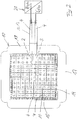
- Figure 2 shows a plan view of the underside, ie the contact side, according to the electrode arrangement Figure 1 .
- This illustration shows that the lattice structure forms square chambers, in the middle of which are the through openings 14 of the lower dielectric layer, which are arranged concentrically with the (larger) through openings 7 of the partial electrodes 2, 3.
- through-channels 7, 14, which are aligned with one another form continuous channels which are bounded on all sides by the material of dielectric 8 and in particular shield the material of sub-electrodes 2, 3 also in the area of through-holes 7.
- the Figure 2 also reveals that the dielectric material is solid in the area of the distance 6 between the partial electrodes 2, 3.
- the grid structure 15 is reinforced outside the region of the partial electrodes 2, 3 with an edge structure 19 made of small chambers arranged in a frame-like manner.
- the supply lines 4 are contacted in a control device 20 by means of a schematically illustrated contact arrangement.
- the leads 4 can be contacted, for example, by cutting contacts, which cut automatically through the material of the dielectric 8 up to the conductive leads 4 and thereby close an insulating housing.
- Such cutting contacts are commercially available and do not need to be explained in more detail here.
- the supply lines are supplied with alternating high voltages, which are shifted with respect to one another with respect to one another in such a way that, in the ideal case, they compensate for one another.
- Enclosing the partial electrodes 2, 3 with their leads 4 with the material of the dielectric 8 can be carried out in the usual way.
- the upper dielectric layer 9 and the lower dielectric layer 10 are formed such that they are welded to one another as a thermoplastic material or can only be glued to one another.
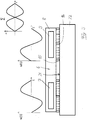
- Figure 3 illustrates schematically that the partial electrodes 2, 3, which are embedded in the dielectric 8 and insulated from one another by the distance 6, in the region of the lattice structure 15, which acts as a spacer, cause the formation of a plasma that is homogeneous in that the the electrical field which triggers the plasma runs homogeneously between the partial electrodes 2, 3 and the surface 21, which is illustrated here by field lines aligned parallel to one another. It also becomes clear that no plasma is formed in the area of the distance 6, because this area is practically field-free. This is due to the fact that the two sub-electrodes 2, 3 are driven with alternating high voltages which are the same in terms of waveform and size, as shown in FIG Figure 3 is shown schematically above the partial electrodes 2, 3.
- the sum curve ⁇ also shown shows that the resulting field in the area of the distance 6 is zero, because the two alternating high voltages ideally cancel each other out to zero. This prevents field phenomena distorting the plasma formation from occurring in the area between the partial electrodes 2, 3. In particular, voltage peaks are avoided.
- the formation of the electrode 1 with two partial electrodes 2, 3 is preferred because it is the easiest to implement. However, for larger surfaces to be treated, it is also conceivable to provide an arrangement with, for example, four partial electrodes, which, for example, form a common square electrode area with four square flat structures 5. The partial electrodes would then be driven diagonally with the same waveforms and adjacent with opposite waveforms.
Landscapes
- Engineering & Computer Science (AREA)
- Physics & Mathematics (AREA)
- Plasma & Fusion (AREA)
- Spectroscopy & Molecular Physics (AREA)
- Health & Medical Sciences (AREA)
- Life Sciences & Earth Sciences (AREA)
- Nuclear Medicine, Radiotherapy & Molecular Imaging (AREA)
- Radiology & Medical Imaging (AREA)
- Biomedical Technology (AREA)
- Animal Behavior & Ethology (AREA)
- General Health & Medical Sciences (AREA)
- Public Health (AREA)
- Veterinary Medicine (AREA)
- Plasma Technology (AREA)
- Physical Or Chemical Processes And Apparatus (AREA)
- Chemical Vapour Deposition (AREA)
- Treatments Of Macromolecular Shaped Articles (AREA)
- Electrotherapy Devices (AREA)
Description
Die Erfindung betrifft eine Elektrodenanordnung zur Ausbildung einer dielektrischen behinderten Plasmaentladung zwischen einer von einer Steuereinrichtung mit einer Wechselhochspannung gespeisten Elektrode und einer zu behandelnden Oberfläche eines elektrisch leitfähigen Körpers, die als Masseelektrode dient, wobei ein Dielektrikum die Elektrode zur zu behandelnden Oberfläche hin vollständig abdeckt und eine Anlageseite für die Oberfläche bildet, wobei die Elektrode aus wenigstens zwei im gleichen Abstand zur Anlageseite nebeneinander angeordneten und durch das Dielektrikum voneinander isolierten Teilelektroden besteht.The invention relates to an electrode arrangement for forming a dielectric disabled plasma discharge between an electrode fed by a control device with an alternating high voltage and a surface of an electrically conductive body to be treated, which serves as a ground electrode, a dielectric completely covering the electrode towards the surface to be treated and one Forms contact side for the surface, the electrode consisting of at least two sub-electrodes arranged at the same distance from the contact side and insulated from one another by the dielectric.
Eine flächige Elektrodenanordnung, die flexibel ausgebildet sein kann, ist durch die
Eine derartige Elektrodenanordnung lässt sich auf die zu behandelnde Oberfläche auflegen, wobei die zu behandelnde Oberfläche insbesondere auf die Haut eines menschlichen oder tierischen Körpers sein kann. Die Plasmabehandlung führt dabei zu einer porentiefen Desinfektion der Haut und verbessert die Aufnahmefähigkeit der Haut für pflegende Stoffe, die auf die behandelte Haut aufgebracht werden.Such an electrode arrangement can be placed on the surface to be treated, the surface to be treated being in particular on the skin of a human or animal body. The plasma treatment leads here to pore-deep disinfection of the skin and improves the skin's absorption capacity for nourishing substances that are applied to the treated skin.
Es ist auch bekannt, dass eine Plasmabehandlung für eine Wundheilung vorteilhaft sein kann. Gemäß
Die
Es sind ferner Elektrodenanordnungen bekannt, mit denen ein dielektrisch behindertes Oberflächenplasma herstellbar ist.
In dieser Hinsicht sind Elektrodenanordnungen vorteilhaft, deren Elektrode so ausgebildet ist, dass zwischen der flächigen Elektrode und der zu behandelnden Oberfläche als Masseelektrode ein weitgehend homogener Feldverlauf entsteht, der zu einem definierten und idealerweise gleichmäßigen Plasma führt.In this regard, electrode arrangements are advantageous, the electrode of which is designed in such a way that a largely homogeneous field profile results between the flat electrode and the surface to be treated as a ground electrode, which leads to a defined and ideally uniform plasma.
Es besteht zunehmend das Bedürfnis, auch vergleichsweise große Flächen durch Auflegen einer - insbesondere flexiblen - Elektrodenanordnung der beschriebenen Art zu behandeln. Mit zunehmender Behandlungsfläche wird es allerdings schwieriger, in üblicher Technik die benötigten Feldstärken für die Ausbildung eines gleichmäßigen Plasmas zwischen der Anlagenseite des Dielektrikums und der zu behandelnden Oberfläche auszubilden. Der Erfindung liegt somit das Problem zu Grunde, eine Elektrodenanordnung der genannten Art so auszubilden, dass einerseits in effizienter Weise ein möglichst gleichmäßiges Plasma ausgebildet wird und andererseits mit einem geringeren Energieaufwand auch größere Flächen mit einer entsprechend großen Elektrodenanordnung behandelt werden können.There is an increasing need to treat even comparatively large areas by placing an — in particular flexible — electrode arrangement of the type described. However, as the treatment area increases, it becomes more difficult to use conventional technology to develop the field strengths required for the formation of a uniform plasma between the system side of the dielectric and the surface to be treated. The invention is therefore based on the problem of designing an electrode arrangement of the type mentioned in such a way that, on the one hand, a plasma which is as uniform as possible is formed and, on the other hand, larger areas can be treated with a correspondingly large electrode arrangement with less energy expenditure.
Zur Lösung dieses Problems ist erfindungsgemäß eine Elektrodenanordnung der eingangs erwähnten Art dadurch gekennzeichnet, dass benachbarte Teilelektroden von der Steuereinrichtung mit bezüglich der Wellenform und der Spannungshöhe gegengleichen, sich kompensierenden Teil-Wechselhochspannungen gespeist werden, wobei die Wechselhochspannungen aus jeweils einem von einem Anregungsimpuls getriggerten hochfrequenten Oszillationsvorgang resultieren.To solve this problem, an electrode arrangement of the type mentioned at the outset is characterized in that adjacent sub-electrodes are supplied by the control device with compensating partial alternating high voltages which are mutually equal with respect to the waveform and the voltage level, the alternating high voltages each consisting of a high-frequency oscillation process triggered by an excitation pulse result.
Die erfindungsgemäße Elektrodenanordnung beruht somit auf dem bekannten Prinzip, die zu behandelnde Oberfläche des elektrisch leitfähigen Körpers als Masseelektrode zu verwenden, sodass prinzipiell für die Ausbildung eines Plasmafelds nur eine einzige Elektrode benötigt wird, die mit der zu behandelnden Oberfläche als Masseelektrode zur Ausbildung des Plasmas zusammenwirkt. Dabei entsteht über die Fläche der Elektrode weitgehend ein idealerweise homogenes elektrisches Feld, in dem die Feldlinien somit parallel zueinander verlaufen. Lediglich am Rand der Elektrode können bekannterweise gekrümmte oder schräg verlaufende Feldlinien entstehen. Bei der erfindungsgemäßen Elektrodenanordnung sind die Teilelektroden vorzugsweise und einer solchen Flächengröße ausgebildet, dass die Ausdehnung des elektrischen Feldes und idealerweise parallelen Feldlinien mehr als 50 %, vorzugsweise mehr als 65 % und weiter bevorzugt mehr als 80 % der Fläche der Teilelektrode beträgt. Die erfindungsgemäßen Elektroden sind flächig ausgedehnt und parallel zur Anlageseite des Dielektrikums positioniert. Erfindungsgemäß sind wenigstens zwei Teilelektroden vorhanden, die separat von der Steuereinrichtung mit Wechselhochspannungen versorgt werden. Die Wechselhochspannungen oszillieren dabei vorzugsweise um das Massepotential herum. Aufgrund der in der Steuereinrichtung vorhandenen Kapazitäten und Induktivitäten sind Schwingkreisanordnungen vorhanden, mit denen ein Anregungsimpuls jeweils einen hochfrequenten Oszillationsvorgang triggert.The electrode arrangement according to the invention is thus based on the known principle of using the surface of the electrically conductive body to be treated as a ground electrode, so that in principle only one electrode is required for the formation of a plasma field, which electrode cooperates with the surface to be treated as a ground electrode for the formation of the plasma . In this case, an ideally homogeneous electric field largely arises over the surface of the electrode, in which the field lines thus run parallel to one another. Only known at the edge of the electrode can be curved or oblique field lines arise. In the electrode arrangement according to the invention, the partial electrodes are preferably of such an area size that the expansion of the electric field and ideally parallel field lines is more than 50%, preferably more than 65% and more preferably more than 80% of the area of the partial electrode. The electrodes according to the invention are extended in area and positioned parallel to the contact side of the dielectric. According to the invention, there are at least two partial electrodes which are supplied with alternating high voltages separately from the control device. The alternating high voltages preferably oscillate around the ground potential. Because of the capacitances and inductivities present in the control device, resonant circuit arrangements are present with which an excitation pulse triggers a high-frequency oscillation process.
Würden die nebeneinander angeordneten Teilelektroden phasengleich angesteuert werden, würde sich im Bereich des homogenen Feldes zwischen der betreffenden Teilelektrode und der zu behandelnden Oberfläche im Idealfall ein homogenes Plasma ausbilden. In dem Verbindungsbereich zwischen den nebeneinander angeordneten Teilelektroden würden sich die Spannungen allerdings addieren und zu unerwünschten Spannungsspitzen führen, die das gleichmäßige Plasmafeld stören würden. Darüber hinaus würden innerhalb des elektrisch leitenden Körper, an der sich zu behandelnde Oberfläche befindet, erhebliche Potentialunterschiede ausbilden, die zu unerwünschten Stromflüssen innerhalb des Körpers führen könnten. Dies kann an einem lebenden Körper zu unangenehmen und gegebenenfalls gefährlichen Erscheinungen führen.If the partial electrodes arranged next to one another were driven in phase, a homogeneous plasma would ideally form in the region of the homogeneous field between the relevant partial electrode and the surface to be treated. In the connection area between the partial electrodes arranged next to one another, however, the voltages would add up and lead to undesired voltage peaks which would disturb the uniform plasma field. In addition, considerable potential differences would form within the electrically conductive body on the surface to be treated, which could lead to undesired current flows within the body. This can lead to unpleasant and possibly dangerous phenomena on a living body.
Erfindungsgemäß ist daher vorgesehen, dass die nebeneinander befindlichen Teilelektroden mit gegengleichen Wechselhochspannungen angesteuert werden, sodass in den Randbereichen der Teilelektroden, die zwischen den benachbarten Teilelektroden liegen, ein im wesentlichen feldfreies Trenngebiet entsteht. Da dieses Trenngebiet schmal und linienförmig sein kann, werden die im Plasma gebildeten desinfizierenden Produkte, beispielsweise die sich in der Luft im Plasma ausbildenden OH-Radikale und Ozonmoleküle, auch in dem Trenngebiet wirksam, da sie auch innerhalb ihrer sehr kurzen Lebensdauer in den Bereich der Oberflächen im Trenngebiet gelangen können.According to the invention, it is therefore provided that the partial electrodes located next to one another are driven with alternating high voltages, so that an essentially field-free separation region is created in the edge regions of the partial electrodes which lie between the adjacent partial electrodes. Since this separation area can be narrow and linear, the disinfectant products formed in the plasma, for example the OH radicals and ozone molecules which form in the air in the plasma, also become effective in the separation area, since they also reach the range of within their very short life Can reach surfaces in the separation area.
Die erfindungsgemäße Elektrodenanordnung mit ihren wenigstens zwei Teilelektroden ist daher so ausgelegt, dass die Teilelektroden über ihre nahezu gesamte Fläche mit der zu behandelnden Oberfläche idealerweise ein im Wesentlichen homogenes Feld - und damit idealerweise ein gleichmäßiges Plasma - ausbildet und zur benachbarten Teilelektrode hin ein schmales prinzipiell feldfreies Trenngebiet entstehen lassen. Für zwei benachbarte Teilelektroden wird daher die eine Teilelektrode mit einer positiven Halbwelle der Wechselhochspannung angesteuert, während die andere Teilelektrode mit einer negativen Halbwelle angesteuert wird, sodass sich im Trenngebiet die beiden Spannungen kompensieren. In einer bevorzugten Ausführungsform sind die jeweiligen Halbwellen in Größe und Form identisch, sodass sich in dem Trenngebiet ein konstantes, sich über die Periode der Wechselhochspannung nicht änderndes Mittenpotential einstellt, das dem Massepotential der Masseelektrode entspricht. In der Praxis kann die Identität der gegengleichen Halbwellen nur angenähert vorliegen, sodass ein konstantes Summenpotential im Trenngebiet auch dann vorliegt, wenn noch eine geringe Schwankung des Summenpotentials vorliegt, die beispielsweise weniger als fünf Prozent der Scheitelspannung beträgt. Das im Idealfall gleichmäßige Plasma kann in der Praxis von geringfügigen Filamententladungen überlagert bzw. gestört sein, auch wenn angestrebt wird, solche Filamententladungen zu vermeiden.The electrode arrangement according to the invention with its at least two partial electrodes is therefore designed such that the partial electrodes ideally form a substantially homogeneous field over their almost entire surface with the surface to be treated - and thus ideally a uniform plasma - and a narrow field-free one in principle towards the neighboring partial electrode Let separation area arise. For two adjacent sub-electrodes, one sub-electrode is therefore driven with a positive half-wave of the alternating high voltage, while the other sub-electrode is driven with a negative half-wave, so that the two voltages are compensated for in the separation region. In a preferred embodiment, the respective half-waves are identical in size and shape, so that a constant center potential that does not change over the period of the alternating high voltage, which corresponds to the ground potential of the ground electrode, is established in the separation region. In practice, the identity of the opposite half-waves can only be approximate, so that there is a constant total potential in the separation region even if there is still a slight fluctuation in the total potential, which is less than five percent of the peak voltage, for example. The ideally uniform plasma can in practice be overlaid or disturbed by slight filament discharges, even if the aim is to avoid such filament discharges.
Die Scheitelspannung der verwendeten Wechselhochspannungen kann zweckmäßigerweise zwischen ± 10 kV und ± 100 kV liegen. Die Wechselfrequenzen der Wechselhochspannungen liegen zweckmäßigerweise zwischen einigen 100 Hz und etwa 100 MHz.The peak voltage of the alternating high voltages used can advantageously be between ± 10 kV and ± 100 kV. The alternating frequencies of the alternating high voltages are expediently between a few 100 Hz and approximately 100 MHz.
Für die Anpassung an ungleichmäßige Oberflächen ist es zweckmäßig, wenn die Teilelektroden und das Dielektrikum flexibel sind. Dadurch kann die gesamte Elektrodenanordnung einer unregelmäßigen Oberfläche folgen, sodass diese im Idealfall mit einem gleichmäßigen Plasmafeld behandelt werden kann.For the adaptation to uneven surfaces, it is expedient if the partial electrodes and the dielectric are flexible. As a result, the entire electrode arrangement can follow an irregular surface, so that it can ideally be treated with a uniform plasma field.
In an sich bekannter Weise kann die Anlageseite des Dielektrikums, die zu der zu behandelnden Oberfläche zeigt, eine Struktur, vorzugsweise in Form eines Gitters oder von Noppen, aufweisen, zwischen denen sich das Plasma ausbilden kann, wenn das Dielektrikum mit der Oberseite der Noppen oder anderer vorstehender Strukturen an der zu behandelnden Oberfläche anliegt.In a manner known per se, the contact side of the dielectric, which faces the surface to be treated, can have a structure, preferably in the form of a grid or nubs, between which the plasma can form, if the dielectric lies with the top of the knobs or other protruding structures on the surface to be treated.
Die erfindungsgemäße Elektrodenanordnung lässt sich auch als Wundauflage ausbilden, wenn das Dielektrikum aus einem wundverträglichen Material, beispielsweise geeigneten Silikonen gebildet ist oder auf die Anlageseite des Dielektrikums eine Schicht aus einem wundverträglichen Material, beispielsweise Gaze, aufgelegt wird.The electrode arrangement according to the invention can also be designed as a wound dressing if the dielectric is formed from a wound-compatible material, for example suitable silicones, or a layer of a wound-compatible material, for example gauze, is placed on the contact side of the dielectric.
Die erfindungsgemäße Elektrodenanordnung eignet sich auch für die Ableitung von Wundflüssigkeit oder für die Zuleitung eines wundheilenden bzw. wundheilungsfördernden Liquids, wenn das Dielektrikum und die Teilelektroden Durchgangsöffnungen aufweisen, die sich in einer Höhenrichtung durch die Elektrodenanordnungen erstrecken und durchgehend von dem die Teilelektroden umgebenden Dielektrikum begrenzt sind.The electrode arrangement according to the invention is also suitable for the drainage of wound fluid or for the supply of a wound-healing or wound-healing-promoting liquid if the dielectric and the partial electrodes have passage openings which extend through the electrode arrangements in a vertical direction and are continuously delimited by the dielectric surrounding the partial electrodes .
Die erfindungsgemäße Elektrodenanordnung weist vorzugsweise bezüglich der Teilelektroden eine hohe Symmetrie auf. Hierzu ist es zweckmäßig, wenn die Teilelektroden eine gleiche Größe aufweisen, sodass die für die Ausbildung des Plasmas wirksame Fläche gleichmäßig auf die Anzahl der Teilelektroden verteilt wird.The electrode arrangement according to the invention preferably has a high symmetry with respect to the partial electrodes. For this purpose, it is expedient if the partial electrodes have the same size, so that the area effective for the formation of the plasma is distributed uniformly over the number of partial electrodes.
Die Teilelektroden können aus einem flachen metallischen Material bestehen, das vorzugsweise beidseitig von einem Dielektrikum abgedeckt wird. Es ist aber auch möglich, die Elektroden durch einen leitfähigen Kunststoff zu realisieren, der sich mit dem ebenfalls durch einen Kunststoff, beispielsweise Silikon, gebildeten Dielektrikum auch formschlüssig verbinden kann. Die Elektrode kann beispielsweise aus einem Silikon mit leitfähigen Zusätzen, in Form von Metallpartikeln, Kohlestoffpartikeln o. ä., bestehen.The partial electrodes can consist of a flat metallic material, which is preferably covered on both sides by a dielectric. However, it is also possible to implement the electrodes by means of a conductive plastic which can also be positively connected to the dielectric which is likewise formed by a plastic, for example silicone. The electrode can, for example, consist of a silicone with conductive additives, in the form of metal particles, carbon particles or the like.
Die Erfindung soll im Folgenden anhand von den Zeichnungen dargestellten Ausführungsbeispielen näher erläutert werden. Es zeigen:
Figur 1- einen Elektrodenaufbau in einer explodierten Darstellung,
Figur 2- eine Draufsicht auf eine fertiggestellte Elektrodenanordnung gemäß
Figur 1 Figur 3- eine schematische Darstellung der Funktion des erfindungsgemäßen Aufbauprinzips.
- Figure 1
- an electrode structure in an exploded view,
- Figure 2
- a plan view of a finished electrode assembly according to
Figure 1 and - Figure 3
- is a schematic representation of the function of the construction principle of the invention.
Gemäß
Die flächigen Gebilde 5 der Teilelektroden 3 weisen eine Anzahl an Durchgangsöffnungen 7 auf, deren Funktion unten näher erläutert wird. Das Material der Teilelektroden kann, wie erwähnt, eine metallische Folie, ein dünnes metallisches Blech oder eine durch den Zusatz von leitenden Partikeln leitend gemachte Kunststoffschicht, insbesondere Silikonschicht, sein.The flat structures 5 of the
Die Elektrode 1 wird allseitig von einem Dielektrikum 8 abgedeckt, das in
Die Durchgangsöffnungen 11 der oberen Dielektrikumsschicht 9 sind konzentrisch mit den Durchgangsöffnungen 7 ausgebildet, weisen jedoch einen kleineren Durchmesser auf, sodass auch im Bereich der Durchgangsöffnungen 7 eine Schicht des Dielektrikums das Material der Teilelektroden 2, 3 abschirmt. Daher ist auch über eine Flüssigkeit keine direkte elektrische Verbindung zu den Teilelektroden 2, 3 herstellbar.The through
Die untere Dielektrikumsschicht 10 bildet, wie die obere Dielektrikumsschicht 9, eine durchgehende zusammenhängende Schicht aus. Die obere Dielektrikumsschicht 9 kann von Durchgangsöffnungen 14 durchbrochen sein. Auch die Durchgangsöffnungen 14 sind konzentrisch mit den Durchgangsöffnungen 7 der Teilelektroden und den Durchgangsöffnungen 11 der oberen Dielektrikumsschicht ausgebildet. Auch in der unteren Dielektrikumsschicht 10 ist der Durchmesser der Durchgangsöffnungen 14 kleiner als der Durchmesser der Durchgangsöffnungen 7 der Teilelektroden 2, 3 und gleich groß wie der Durchmesser der Durchgangsöffnungen 11 der oberen Dielektrikumsschicht 9.The lower
Auf der von den Teilelektroden 2, 3 abgewandten Seite bildet die untere Dielektrikumsschicht 10 eine Gitterstruktur 15 mit sich kreuzenden stegartigen Wänden aus, deren freie Kanten 16 eine Anlageseite definieren, mit der eine Elektrodenanordnung auf einer zu behandelnden Oberfläche aufliegen kann.On the side facing away from the
Die
In
Das Umschließen der Teilelektroden 2, 3 mit ihren Zuleitungen 4 mit dem Material des Dielektrikums 8 kann in üblicher Weise erfolgen. In der Anordnung gemäß
Die Ausbildung der Elektrode 1 mit zwei Teilelektroden 2, 3 ist bevorzugt, weil sie am einfachsten zu realisieren ist. Es ist aber für größere zu behandelnde Oberflächen denkbar, auch eine Anordnung mit beispielsweise vier Teilelektroden vorzusehen, die beispielsweise mit vier quadratischen flächigen Gebilden 5 eine gemeinsam quadratische Elektrodenfläche ausbilden. Die Ansteuerung der Teilelektroden würde dann diagonal mit gleichen Wellenformen und benachbart mit gegengleichen Wellenformen erfolgen.The formation of the
Selbstverständlich sind auch andere Geometrien der Teilelektroden denkbar, beispielsweise in Form von Dreiecken, Rauten, Sechsecken oder auch Kreisflächen.Of course, other geometries of the partial electrodes are also conceivable, for example in the form of triangles, rhombuses, hexagons or even circular surfaces.
Claims (8)
- Electrode arrangement for forming a dielectric barrier plasma discharge between an electrode (1), which is fed with a high AC voltage by a control device (20), and a surface (21) to be treated of an electrically conductive body (22), wherein a dielectric (8) completely covers the electrode (1) towards the surface (21) to be treated and forms a contact side for the surface (21), wherein the electrode (1) consists of at least two partial electrodes (2, 3) arranged next to each other at the same distance (6) from the contact side and insulated from each other by the dielectric (8), and wherein adjacent partial electrodes (2, 3) are fed by the control device with mutually compensating partial high AC voltages that are equal and opposite to each other with respect to waveform and voltage magnitude, characterized in that the electrically conductive body (22) serves as a ground electrode and wherein the high AC voltages result in each case from a high-frequency oscillation process triggered by an excitation impulse.
- Electrode arrangement according to claim 1, characterized in that the sum of the partial high AC voltages fed to adjacent partial electrodes (2, 3) forms a value which is constant over time and which corresponds to the potential of the ground electrode.
- Electrode arrangement according to claims 1 and 2, characterized in that the partial electrodes (2, 3) and the dielectric (8) covering them have a planar surface (21).
- Electrode arrangement according to one of claims 1 to 3, characterized in that the partial electrodes (2, 3) and the dielectric (8) are flexible.
- Electrode arrangement according to one of claims 1 to 4, characterized in that the contact side of the dielectric (8) facing the surface (21) to be treated has a structure which forms interspaces when the electrode arrangement is in contact with the surface (21) to be treated.
- Electrode arrangement according to one of claims 1 to 5, characterized in that the dielectric (8) and the partial electrodes (2, 3) have through openings (14) which extend in a height direction through the electrode arrangement and are delimited continuously by the dielectric (8) surrounding the partial electrodes (2, 3).
- Electrode arrangement according to any one of claims 1 to 6, characterized in that the partial electrodes (2, 3) have the same size.
- Electrode arrangement according to one of claims 1 to 7, characterized in that the peak voltages of the high AC voltages are between +/- 10 kV and +/- 100 kV.
Priority Applications (1)
| Application Number | Priority Date | Filing Date | Title |
|---|---|---|---|
| PL18200611T PL3448130T3 (en) | 2016-09-30 | 2017-07-21 | Electrode assembly for forming a dielectrically impeded plasma discharge |
Applications Claiming Priority (3)
| Application Number | Priority Date | Filing Date | Title |
|---|---|---|---|
| DE102016118569.8A DE102016118569A1 (en) | 2016-09-30 | 2016-09-30 | Electrode arrangement for forming a dielectrically impeded plasma discharge |
| EP17754249.5A EP3320759B1 (en) | 2016-09-30 | 2017-07-21 | Electrode arrangement for forming a dielectric barrier plasma discharge |
| PCT/DE2017/100612 WO2018059612A1 (en) | 2016-09-30 | 2017-07-21 | Electrode arrangement for forming a dielectric barrier plasma discharge |
Related Parent Applications (2)
| Application Number | Title | Priority Date | Filing Date |
|---|---|---|---|
| EP17754249.5A Division EP3320759B1 (en) | 2016-09-30 | 2017-07-21 | Electrode arrangement for forming a dielectric barrier plasma discharge |
| EP17754249.5A Division-Into EP3320759B1 (en) | 2016-09-30 | 2017-07-21 | Electrode arrangement for forming a dielectric barrier plasma discharge |
Publications (2)
| Publication Number | Publication Date |
|---|---|
| EP3448130A1 EP3448130A1 (en) | 2019-02-27 |
| EP3448130B1 true EP3448130B1 (en) | 2020-04-08 |
Family
ID=59655806
Family Applications (2)
| Application Number | Title | Priority Date | Filing Date |
|---|---|---|---|
| EP18200611.4A Active EP3448130B1 (en) | 2016-09-30 | 2017-07-21 | Electrode assembly for forming a dielectrically impeded plasma discharge |
| EP17754249.5A Active EP3320759B1 (en) | 2016-09-30 | 2017-07-21 | Electrode arrangement for forming a dielectric barrier plasma discharge |
Family Applications After (1)
| Application Number | Title | Priority Date | Filing Date |
|---|---|---|---|
| EP17754249.5A Active EP3320759B1 (en) | 2016-09-30 | 2017-07-21 | Electrode arrangement for forming a dielectric barrier plasma discharge |
Country Status (14)
| Country | Link |
|---|---|
| US (1) | US11785700B2 (en) |
| EP (2) | EP3448130B1 (en) |
| JP (1) | JP7074351B2 (en) |
| KR (1) | KR102460970B1 (en) |
| CN (1) | CN109792832A (en) |
| BR (1) | BR112019001274B1 (en) |
| DE (1) | DE102016118569A1 (en) |
| DK (1) | DK3448130T3 (en) |
| ES (2) | ES2797948T3 (en) |
| MX (1) | MX2019000934A (en) |
| PL (1) | PL3448130T3 (en) |
| RU (1) | RU2737280C2 (en) |
| TR (1) | TR201901068T4 (en) |
| WO (1) | WO2018059612A1 (en) |
Families Citing this family (12)
| Publication number | Priority date | Publication date | Assignee | Title |
|---|---|---|---|---|
| DE102016118569A1 (en) * | 2016-09-30 | 2018-04-05 | Cinogy Gmbh | Electrode arrangement for forming a dielectrically impeded plasma discharge |
| NL2017822B1 (en) * | 2016-11-18 | 2018-05-25 | Plasmacure B V | Non-Thermal Plasma Device with electromagnetic compatibility control |
| DE102017100192A1 (en) * | 2017-01-06 | 2018-07-12 | Cinogy Gmbh | Permanent wound dressing with plasma electrode |
| KR101813558B1 (en) * | 2017-04-12 | 2018-01-03 | 주식회사 서린메디케어 | Skin treatment apparatus using fractional plasma |
| DE102019109940B4 (en) | 2019-04-15 | 2020-12-10 | Cinogy Gmbh | Treatment arrangement for the treatment of a surface of a body with a dielectrically impeded plasma |
| NL2027148B1 (en) * | 2020-12-17 | 2022-07-11 | Plasmacure B V | Treatment pad for a dielectric barrier discharge plasma treatment |
| DE102021123900A1 (en) | 2021-09-15 | 2023-03-16 | Cinogy Gmbh | Footwear with an electrode arrangement for generating plasma |
| DE102021124377A1 (en) | 2021-09-21 | 2023-03-23 | Cinogy Gmbh | Electrode arrangement for a plasma discharge |
| DE102022105186A1 (en) | 2022-03-04 | 2023-09-07 | Cinogy Gmbh | wound dressing |
| DE102022124101A1 (en) | 2022-09-20 | 2024-03-21 | Cinogy Gmbh | Plasma treatment arrangement |
| DE102023104707B3 (en) | 2023-02-27 | 2024-05-02 | Cinogy Gmbh | Plasma treatment arrangement |
| DE102023104705A1 (en) | 2023-02-27 | 2024-08-29 | Cinogy Gmbh | Plasma treatment arrangement |
Family Cites Families (36)
| Publication number | Priority date | Publication date | Assignee | Title |
|---|---|---|---|---|
| DE19532105C2 (en) * | 1994-08-30 | 2002-11-14 | Fraunhofer Ges Forschung | Method and device for treating three-dimensional workpieces with a direct barrier discharge and method for producing an electrode provided with a barrier for this barrier discharge |
| US6146599A (en) * | 1999-02-24 | 2000-11-14 | Seagate Technology Llc | Dielectric barrier discharge system and method for decomposing hazardous compounds in fluids |
| JP2005509255A (en) * | 2001-11-02 | 2005-04-07 | プラズマゾル・コーポレイション | Non-thermal plasma slit discharge device |
| DE112004000057B4 (en) | 2003-05-27 | 2008-09-25 | Matsushita Electric Works, Ltd., Kadoma | Plasma treatment apparatus and plasma treatment method |
| JP4603326B2 (en) | 2004-09-21 | 2010-12-22 | 積水化学工業株式会社 | Surface treatment equipment |
| JP2006302625A (en) * | 2005-04-19 | 2006-11-02 | Matsushita Electric Works Ltd | Plasma treatment device and method |
| DE102005029360B4 (en) * | 2005-06-24 | 2011-11-10 | Softal Corona & Plasma Gmbh | Two methods for continuous atmospheric pressure Plasma treatment of workpieces, in particular material plates or sheets |
| SK51082006A3 (en) * | 2006-12-05 | 2008-07-07 | Fakulta Matematiky, Fyziky A Informatiky Univerzitfakulta Matematiky, Fyziky A Informatiky Univerzity Komensk�Hoy Komensk�Ho | Apparatus and treatment method of surface of metals and metalloids, oxides of metals and oxides of metalloids and nitrides of metalloids |
| DE102007030915A1 (en) * | 2007-07-03 | 2009-01-22 | Cinogy Gmbh | Device for the treatment of surfaces with a plasma generated by means of an electrode via a solid dielectric by a dielectrically impeded gas discharge |
| JP5466951B2 (en) * | 2008-01-18 | 2014-04-09 | 京セラ株式会社 | Plasma generator, discharge device and reactor using plasma generator |
| WO2009098662A1 (en) | 2008-02-08 | 2009-08-13 | Ecole Polytechnique Federale De Lausanne (Epfl) | Long lifetime system for the generation of surface plasmas |
| EP2205049A1 (en) * | 2008-12-30 | 2010-07-07 | Nederlandse Organisatie voor toegepast-natuurwetenschappelijk Onderzoek TNO | Apparatus and method for treating an object |
| CN102282916A (en) * | 2009-01-13 | 2011-12-14 | 里巴贝鲁株式会社 | Apparatus and method for producing plasma |
| DE102009047220A1 (en) * | 2009-11-27 | 2011-06-01 | Leibniz-Institut für Plasmaforschung und Technologie e.V. | Apparatus and method for generating a pulsed anisothermic atmospheric pressure plasma |
| DE102009060627B4 (en) * | 2009-12-24 | 2014-06-05 | Cinogy Gmbh | Electrode arrangement for a dielectrically impeded plasma treatment |
| KR101112741B1 (en) * | 2010-04-20 | 2012-02-22 | 다이나믹솔라디자인 주식회사 | Plasma chamber having power feeding device for multi divided electrode set |
| DE102010024086A1 (en) | 2010-06-17 | 2011-12-22 | WPNLB UG (haftungsbeschränkt) & Co. KG | Apparatus for continuous plasma treatment and / or plasma coating of a piece of material |
| EP2608329A4 (en) * | 2010-08-18 | 2014-10-22 | Kyocera Corp | Ionic wind generating body and ionic wind generating device |
| US8766177B2 (en) * | 2010-10-11 | 2014-07-01 | University Of North Texas | Nanomanipulation coupled nanospray mass spectrometry (NMS) |
| DE102011000261A1 (en) * | 2011-01-21 | 2012-07-26 | Hochschule für angewandte Wissenschaft und Kunst Fachhochschule Hildesheim/Holzminden/Göttingen | Dielectric coplanar discharge source for surface treatment under atmospheric pressure |
| US9387269B2 (en) * | 2011-01-28 | 2016-07-12 | Bovie Medical Corporation | Cold plasma jet hand sanitizer |
| DE102011010273A1 (en) * | 2011-02-02 | 2012-08-02 | Cinogy Gmbh | Method for treating human or animal hair and apparatus for carrying out the method |
| DE102011001416A1 (en) | 2011-03-18 | 2012-09-20 | Manfred H. Langner | Plasma treatment device for treating surfaces e.g. wounds of skin i.e. forearm skin, of patient outside of hospitals, has oxygen reducing layer detachably secured on outer side of electrode, where outer side is turned away from surface |
| DE102011076806A1 (en) * | 2011-05-31 | 2012-12-06 | Leibniz-Institut für Plasmaforschung und Technologie e.V. | Apparatus and method for producing a cold, homogeneous plasma under atmospheric pressure conditions |
| WO2013108047A2 (en) * | 2012-01-20 | 2013-07-25 | University Of Newcastle Upon Tyne | Integrated intensified biorefinery for gas-to-liquid conversion |
| WO2014010851A1 (en) * | 2012-07-13 | 2014-01-16 | 주식회사 에스피텍 | Dielectric barrier discharge-type electrode structure for generating plasma having conductive body protrusion on electrodes |
| US9536709B2 (en) * | 2013-02-04 | 2017-01-03 | Creative Technology Corporation | Plasma generator |
| RU2526810C1 (en) * | 2013-02-12 | 2014-08-27 | Федеральное государственное бюджетное образовательное учреждение высшего профессионального образования "Санкт-Петербургский государственный университет" (СПбГУ) | Plasma disinfector for biological tissues |
| JP6180016B2 (en) | 2013-04-23 | 2017-08-16 | 沖野 晃俊 | Biological cell and skin care equipment using atmospheric pressure plasma |
| WO2015088948A1 (en) * | 2013-12-09 | 2015-06-18 | EP Technologies LLC | Shape conforming flexible dielectric barrier discharge plasma generators |
| JP6600632B2 (en) | 2013-12-27 | 2019-10-30 | モー メディカル デバイセス エルエルシー | Application of electric field therapy to body parts |
| DE102014013716B4 (en) * | 2014-09-11 | 2022-04-07 | Cinogy Gmbh | Electrode arrangement for forming a dielectric barrier plasma discharge |
| JP2016140857A (en) * | 2015-02-05 | 2016-08-08 | 株式会社東芝 | Airflow generation device |
| DE102016118569A1 (en) * | 2016-09-30 | 2018-04-05 | Cinogy Gmbh | Electrode arrangement for forming a dielectrically impeded plasma discharge |
| DE102017106570A1 (en) * | 2017-03-28 | 2018-10-04 | Cinogy Gmbh | Flat flexible support arrangement |
| DE102019101063B4 (en) * | 2019-01-16 | 2021-02-25 | Cinogy Gmbh | Plasma treatment arrangement and method for adapting the size of a support surface of the plasma treatment arrangement to the size of the surface to be treated |
-
2016
- 2016-09-30 DE DE102016118569.8A patent/DE102016118569A1/en not_active Withdrawn
-
2017
- 2017-07-21 BR BR112019001274-5A patent/BR112019001274B1/en active IP Right Grant
- 2017-07-21 WO PCT/DE2017/100612 patent/WO2018059612A1/en unknown
- 2017-07-21 RU RU2019103085A patent/RU2737280C2/en active
- 2017-07-21 DK DK18200611.4T patent/DK3448130T3/en active
- 2017-07-21 MX MX2019000934A patent/MX2019000934A/en unknown
- 2017-07-21 TR TR2019/01068T patent/TR201901068T4/en unknown
- 2017-07-21 ES ES18200611T patent/ES2797948T3/en active Active
- 2017-07-21 CN CN201780051231.7A patent/CN109792832A/en active Pending
- 2017-07-21 KR KR1020197011055A patent/KR102460970B1/en active IP Right Grant
- 2017-07-21 US US16/329,455 patent/US11785700B2/en active Active
- 2017-07-21 ES ES17754249T patent/ES2710316T3/en active Active
- 2017-07-21 EP EP18200611.4A patent/EP3448130B1/en active Active
- 2017-07-21 EP EP17754249.5A patent/EP3320759B1/en active Active
- 2017-07-21 PL PL18200611T patent/PL3448130T3/en unknown
- 2017-07-21 JP JP2019505236A patent/JP7074351B2/en active Active
Non-Patent Citations (1)
| Title |
|---|
| None * |
Also Published As
| Publication number | Publication date |
|---|---|
| RU2737280C2 (en) | 2020-11-26 |
| DK3448130T3 (en) | 2020-06-29 |
| KR20190055165A (en) | 2019-05-22 |
| KR102460970B1 (en) | 2022-10-31 |
| MX2019000934A (en) | 2019-07-04 |
| US20190223280A1 (en) | 2019-07-18 |
| BR112019001274A2 (en) | 2019-04-30 |
| ES2797948T3 (en) | 2020-12-04 |
| JP7074351B2 (en) | 2022-05-24 |
| EP3320759A1 (en) | 2018-05-16 |
| CN109792832A (en) | 2019-05-21 |
| DE102016118569A1 (en) | 2018-04-05 |
| JP2019530948A (en) | 2019-10-24 |
| EP3448130A1 (en) | 2019-02-27 |
| PL3448130T3 (en) | 2020-10-19 |
| TR201901068T4 (en) | 2019-02-21 |
| US11785700B2 (en) | 2023-10-10 |
| BR112019001274B1 (en) | 2023-03-14 |
| ES2710316T3 (en) | 2019-04-24 |
| RU2019103085A (en) | 2020-10-30 |
| WO2018059612A1 (en) | 2018-04-05 |
| RU2019103085A3 (en) | 2020-10-30 |
| EP3320759B1 (en) | 2019-01-02 |
Similar Documents
| Publication | Publication Date | Title |
|---|---|---|
| EP3448130B1 (en) | Electrode assembly for forming a dielectrically impeded plasma discharge | |
| EP3566552B1 (en) | Flat flexible support piece for a dielectrically impeded plasma treatment | |
| DE102009060627B4 (en) | Electrode arrangement for a dielectrically impeded plasma treatment | |
| EP3192333B1 (en) | Electrode arrangement for forming a dielectric barrier plasma discharge | |
| DE102016108450B4 (en) | Treatment arrangement and method for producing a treatment arrangement | |
| EP2163143B1 (en) | Device for the treatment of surfaces with a plasma generated by an electrode over a solid dielectric via a dielectric barrier gas discharge | |
| EP3171676B1 (en) | Plasma generating device, plasma generating system and method of generating plasma | |
| EP2723447A1 (en) | Electrode arrangement for a dielectrically limited gas discharge | |
| EP1106033A1 (en) | Heating member with resistive surface | |
| EP3630279B1 (en) | Flat pad structure configured to generate a dielectric barrier plasma discharge | |
| WO2018162003A1 (en) | Planar flexible electrode arrangement for a dielectric barrier plasma discharge | |
| DE102018126492A1 (en) | Plasma treatment device | |
| DE102013112316A1 (en) | Piezoelectric transformer and counter electrode | |
| DE202018106346U1 (en) | Plasma treatment device | |
| DE102016107550B4 (en) | Method and device for the thermal treatment of solids | |
| EP4406367A1 (en) | Electrode assembly for a plasma discharge | |
| WO2000003466A1 (en) | Device for generating ionized gases using corona discharges | |
| DE29911754U1 (en) | Device for generating ionized gases by means of corona discharges | |
| DE1232649B (en) | Device for producing an adhesion between solids | |
| DE10148775A1 (en) | Application unit, useful in supplying therapeutic substances to tumor cells, comprises an electrical unit for producing a pulsed electrical field |
Legal Events
| Date | Code | Title | Description |
|---|---|---|---|
| PUAI | Public reference made under article 153(3) epc to a published international application that has entered the european phase |
Free format text: ORIGINAL CODE: 0009012 |
|
| STAA | Information on the status of an ep patent application or granted ep patent |
Free format text: STATUS: THE APPLICATION HAS BEEN PUBLISHED |
|
| AC | Divisional application: reference to earlier application |
Ref document number: 3320759 Country of ref document: EP Kind code of ref document: P |
|
| AK | Designated contracting states |
Kind code of ref document: A1 Designated state(s): AL AT BE BG CH CY CZ DE DK EE ES FI FR GB GR HR HU IE IS IT LI LT LU LV MC MK MT NL NO PL PT RO RS SE SI SK SM TR |
|
| AX | Request for extension of the european patent |
Extension state: BA ME |
|
| STAA | Information on the status of an ep patent application or granted ep patent |
Free format text: STATUS: REQUEST FOR EXAMINATION WAS MADE |
|
| 17P | Request for examination filed |
Effective date: 20190730 |
|
| RBV | Designated contracting states (corrected) |
Designated state(s): AL AT BE BG CH CY CZ DE DK EE ES FI FR GB GR HR HU IE IS IT LI LT LU LV MC MK MT NL NO PL PT RO RS SE SI SK SM TR |
|
| GRAJ | Information related to disapproval of communication of intention to grant by the applicant or resumption of examination proceedings by the epo deleted |
Free format text: ORIGINAL CODE: EPIDOSDIGR1 |
|
| STAA | Information on the status of an ep patent application or granted ep patent |
Free format text: STATUS: GRANT OF PATENT IS INTENDED |
|
| GRAP | Despatch of communication of intention to grant a patent |
Free format text: ORIGINAL CODE: EPIDOSNIGR1 |
|
| RIC1 | Information provided on ipc code assigned before grant |
Ipc: H05H 1/24 20060101AFI20191030BHEP |
|
| INTG | Intention to grant announced |
Effective date: 20191112 |
|
| GRAS | Grant fee paid |
Free format text: ORIGINAL CODE: EPIDOSNIGR3 |
|
| GRAA | (expected) grant |
Free format text: ORIGINAL CODE: 0009210 |
|
| STAA | Information on the status of an ep patent application or granted ep patent |
Free format text: STATUS: THE PATENT HAS BEEN GRANTED |
|
| AC | Divisional application: reference to earlier application |
Ref document number: 3320759 Country of ref document: EP Kind code of ref document: P |
|
| AK | Designated contracting states |
Kind code of ref document: B1 Designated state(s): AL AT BE BG CH CY CZ DE DK EE ES FI FR GB GR HR HU IE IS IT LI LT LU LV MC MK MT NL NO PL PT RO RS SE SI SK SM TR |
|
| REG | Reference to a national code |
Ref country code: AT Ref legal event code: REF Ref document number: 1256164 Country of ref document: AT Kind code of ref document: T Effective date: 20200415 Ref country code: CH Ref legal event code: EP |
|
| REG | Reference to a national code |
Ref country code: DE Ref legal event code: R096 Ref document number: 502017004691 Country of ref document: DE |
|
| REG | Reference to a national code |
Ref country code: IE Ref legal event code: FG4D Free format text: LANGUAGE OF EP DOCUMENT: GERMAN |
|
| REG | Reference to a national code |
Ref country code: DK Ref legal event code: T3 Effective date: 20200625 |
|
| REG | Reference to a national code |
Ref country code: CH Ref legal event code: NV Representative=s name: BRAUNPAT BRAUN EDER AG, CH |
|
| REG | Reference to a national code |
Ref country code: SE Ref legal event code: TRGR |
|
| REG | Reference to a national code |
Ref country code: NL Ref legal event code: FP |
|
| REG | Reference to a national code |
Ref country code: LT Ref legal event code: MG4D |
|
| PG25 | Lapsed in a contracting state [announced via postgrant information from national office to epo] |
Ref country code: LT Free format text: LAPSE BECAUSE OF FAILURE TO SUBMIT A TRANSLATION OF THE DESCRIPTION OR TO PAY THE FEE WITHIN THE PRESCRIBED TIME-LIMIT Effective date: 20200408 Ref country code: GR Free format text: LAPSE BECAUSE OF FAILURE TO SUBMIT A TRANSLATION OF THE DESCRIPTION OR TO PAY THE FEE WITHIN THE PRESCRIBED TIME-LIMIT Effective date: 20200709 Ref country code: PT Free format text: LAPSE BECAUSE OF FAILURE TO SUBMIT A TRANSLATION OF THE DESCRIPTION OR TO PAY THE FEE WITHIN THE PRESCRIBED TIME-LIMIT Effective date: 20200817 Ref country code: NO Free format text: LAPSE BECAUSE OF FAILURE TO SUBMIT A TRANSLATION OF THE DESCRIPTION OR TO PAY THE FEE WITHIN THE PRESCRIBED TIME-LIMIT Effective date: 20200708 Ref country code: FI Free format text: LAPSE BECAUSE OF FAILURE TO SUBMIT A TRANSLATION OF THE DESCRIPTION OR TO PAY THE FEE WITHIN THE PRESCRIBED TIME-LIMIT Effective date: 20200408 Ref country code: IS Free format text: LAPSE BECAUSE OF FAILURE TO SUBMIT A TRANSLATION OF THE DESCRIPTION OR TO PAY THE FEE WITHIN THE PRESCRIBED TIME-LIMIT Effective date: 20200808 |
|
| PG25 | Lapsed in a contracting state [announced via postgrant information from national office to epo] |
Ref country code: HR Free format text: LAPSE BECAUSE OF FAILURE TO SUBMIT A TRANSLATION OF THE DESCRIPTION OR TO PAY THE FEE WITHIN THE PRESCRIBED TIME-LIMIT Effective date: 20200408 Ref country code: RS Free format text: LAPSE BECAUSE OF FAILURE TO SUBMIT A TRANSLATION OF THE DESCRIPTION OR TO PAY THE FEE WITHIN THE PRESCRIBED TIME-LIMIT Effective date: 20200408 Ref country code: BG Free format text: LAPSE BECAUSE OF FAILURE TO SUBMIT A TRANSLATION OF THE DESCRIPTION OR TO PAY THE FEE WITHIN THE PRESCRIBED TIME-LIMIT Effective date: 20200708 Ref country code: LV Free format text: LAPSE BECAUSE OF FAILURE TO SUBMIT A TRANSLATION OF THE DESCRIPTION OR TO PAY THE FEE WITHIN THE PRESCRIBED TIME-LIMIT Effective date: 20200408 |
|
| REG | Reference to a national code |
Ref country code: ES Ref legal event code: FG2A Ref document number: 2797948 Country of ref document: ES Kind code of ref document: T3 Effective date: 20201204 |
|
| PG25 | Lapsed in a contracting state [announced via postgrant information from national office to epo] |
Ref country code: AL Free format text: LAPSE BECAUSE OF FAILURE TO SUBMIT A TRANSLATION OF THE DESCRIPTION OR TO PAY THE FEE WITHIN THE PRESCRIBED TIME-LIMIT Effective date: 20200408 |
|
| REG | Reference to a national code |
Ref country code: DE Ref legal event code: R097 Ref document number: 502017004691 Country of ref document: DE |
|
| PG25 | Lapsed in a contracting state [announced via postgrant information from national office to epo] |
Ref country code: CZ Free format text: LAPSE BECAUSE OF FAILURE TO SUBMIT A TRANSLATION OF THE DESCRIPTION OR TO PAY THE FEE WITHIN THE PRESCRIBED TIME-LIMIT Effective date: 20200408 Ref country code: SM Free format text: LAPSE BECAUSE OF FAILURE TO SUBMIT A TRANSLATION OF THE DESCRIPTION OR TO PAY THE FEE WITHIN THE PRESCRIBED TIME-LIMIT Effective date: 20200408 Ref country code: EE Free format text: LAPSE BECAUSE OF FAILURE TO SUBMIT A TRANSLATION OF THE DESCRIPTION OR TO PAY THE FEE WITHIN THE PRESCRIBED TIME-LIMIT Effective date: 20200408 Ref country code: RO Free format text: LAPSE BECAUSE OF FAILURE TO SUBMIT A TRANSLATION OF THE DESCRIPTION OR TO PAY THE FEE WITHIN THE PRESCRIBED TIME-LIMIT Effective date: 20200408 |
|
| PLBE | No opposition filed within time limit |
Free format text: ORIGINAL CODE: 0009261 |
|
| STAA | Information on the status of an ep patent application or granted ep patent |
Free format text: STATUS: NO OPPOSITION FILED WITHIN TIME LIMIT |
|
| PG25 | Lapsed in a contracting state [announced via postgrant information from national office to epo] |
Ref country code: MC Free format text: LAPSE BECAUSE OF FAILURE TO SUBMIT A TRANSLATION OF THE DESCRIPTION OR TO PAY THE FEE WITHIN THE PRESCRIBED TIME-LIMIT Effective date: 20200408 Ref country code: SK Free format text: LAPSE BECAUSE OF FAILURE TO SUBMIT A TRANSLATION OF THE DESCRIPTION OR TO PAY THE FEE WITHIN THE PRESCRIBED TIME-LIMIT Effective date: 20200408 |
|
| 26N | No opposition filed |
Effective date: 20210112 |
|
| REG | Reference to a national code |
Ref country code: BE Ref legal event code: MM Effective date: 20200731 |
|
| PG25 | Lapsed in a contracting state [announced via postgrant information from national office to epo] |
Ref country code: LU Free format text: LAPSE BECAUSE OF NON-PAYMENT OF DUE FEES Effective date: 20200721 |
|
| PG25 | Lapsed in a contracting state [announced via postgrant information from national office to epo] |
Ref country code: BE Free format text: LAPSE BECAUSE OF NON-PAYMENT OF DUE FEES Effective date: 20200731 Ref country code: SI Free format text: LAPSE BECAUSE OF FAILURE TO SUBMIT A TRANSLATION OF THE DESCRIPTION OR TO PAY THE FEE WITHIN THE PRESCRIBED TIME-LIMIT Effective date: 20200408 |
|
| PG25 | Lapsed in a contracting state [announced via postgrant information from national office to epo] |
Ref country code: IE Free format text: LAPSE BECAUSE OF NON-PAYMENT OF DUE FEES Effective date: 20200721 |
|
| PG25 | Lapsed in a contracting state [announced via postgrant information from national office to epo] |
Ref country code: MT Free format text: LAPSE BECAUSE OF FAILURE TO SUBMIT A TRANSLATION OF THE DESCRIPTION OR TO PAY THE FEE WITHIN THE PRESCRIBED TIME-LIMIT Effective date: 20200408 Ref country code: CY Free format text: LAPSE BECAUSE OF FAILURE TO SUBMIT A TRANSLATION OF THE DESCRIPTION OR TO PAY THE FEE WITHIN THE PRESCRIBED TIME-LIMIT Effective date: 20200408 |
|
| PG25 | Lapsed in a contracting state [announced via postgrant information from national office to epo] |
Ref country code: MK Free format text: LAPSE BECAUSE OF FAILURE TO SUBMIT A TRANSLATION OF THE DESCRIPTION OR TO PAY THE FEE WITHIN THE PRESCRIBED TIME-LIMIT Effective date: 20200408 |
|
| PGFP | Annual fee paid to national office [announced via postgrant information from national office to epo] |
Ref country code: SE Payment date: 20230315 Year of fee payment: 7 |
|
| P01 | Opt-out of the competence of the unified patent court (upc) registered |
Effective date: 20230526 |
|
| REG | Reference to a national code |
Ref country code: AT Ref legal event code: MM01 Ref document number: 1256164 Country of ref document: AT Kind code of ref document: T Effective date: 20220721 |
|
| PG25 | Lapsed in a contracting state [announced via postgrant information from national office to epo] |
Ref country code: AT Free format text: LAPSE BECAUSE OF NON-PAYMENT OF DUE FEES Effective date: 20220721 |
|
| PGFP | Annual fee paid to national office [announced via postgrant information from national office to epo] |
Ref country code: TR Payment date: 20230719 Year of fee payment: 7 Ref country code: IT Payment date: 20230731 Year of fee payment: 7 Ref country code: GB Payment date: 20230724 Year of fee payment: 7 Ref country code: ES Payment date: 20230821 Year of fee payment: 7 Ref country code: CH Payment date: 20230801 Year of fee payment: 7 |
|
| PGFP | Annual fee paid to national office [announced via postgrant information from national office to epo] |
Ref country code: PL Payment date: 20230710 Year of fee payment: 7 Ref country code: FR Payment date: 20230720 Year of fee payment: 7 Ref country code: DK Payment date: 20230724 Year of fee payment: 7 Ref country code: DE Payment date: 20230329 Year of fee payment: 7 |
|
| PGFP | Annual fee paid to national office [announced via postgrant information from national office to epo] |
Ref country code: NL Payment date: 20240722 Year of fee payment: 8 |