EP3435482B1 - Liaison de connexion comprenant un système de câble et un système de plaque, procédé de fabrication d'une telle liaison de connexion - Google Patents
Liaison de connexion comprenant un système de câble et un système de plaque, procédé de fabrication d'une telle liaison de connexion Download PDFInfo
- Publication number
- EP3435482B1 EP3435482B1 EP17183028.4A EP17183028A EP3435482B1 EP 3435482 B1 EP3435482 B1 EP 3435482B1 EP 17183028 A EP17183028 A EP 17183028A EP 3435482 B1 EP3435482 B1 EP 3435482B1
- Authority
- EP
- European Patent Office
- Prior art keywords
- cable
- inner conductor
- connection
- outer layer
- conductor
- Prior art date
- Legal status (The legal status is an assumption and is not a legal conclusion. Google has not performed a legal analysis and makes no representation as to the accuracy of the status listed.)
- Active
Links
- 238000004519 manufacturing process Methods 0.000 title claims description 15
- 239000004020 conductor Substances 0.000 claims description 313
- 238000000034 method Methods 0.000 claims description 35
- 229910000679 solder Inorganic materials 0.000 claims description 35
- 229910052751 metal Inorganic materials 0.000 claims description 20
- 239000002184 metal Substances 0.000 claims description 20
- 239000004033 plastic Substances 0.000 claims description 12
- 239000003989 dielectric material Substances 0.000 claims description 7
- 239000000463 material Substances 0.000 claims description 5
- 238000003754 machining Methods 0.000 claims description 3
- 239000011248 coating agent Substances 0.000 claims 1
- 238000000576 coating method Methods 0.000 claims 1
- 238000010438 heat treatment Methods 0.000 claims 1
- 238000010348 incorporation Methods 0.000 claims 1
- 239000000155 melt Substances 0.000 claims 1
- 210000002105 tongue Anatomy 0.000 description 17
- 238000005476 soldering Methods 0.000 description 15
- 239000011888 foil Substances 0.000 description 10
- 238000010276 construction Methods 0.000 description 5
- RYGMFSIKBFXOCR-UHFFFAOYSA-N Copper Chemical compound [Cu] RYGMFSIKBFXOCR-UHFFFAOYSA-N 0.000 description 3
- 239000000969 carrier Substances 0.000 description 3
- 229910052802 copper Inorganic materials 0.000 description 3
- 239000010949 copper Substances 0.000 description 3
- 238000005553 drilling Methods 0.000 description 3
- 230000033001 locomotion Effects 0.000 description 3
- 238000003801 milling Methods 0.000 description 3
- XEEYBQQBJWHFJM-UHFFFAOYSA-N Iron Chemical compound [Fe] XEEYBQQBJWHFJM-UHFFFAOYSA-N 0.000 description 2
- 238000004026 adhesive bonding Methods 0.000 description 2
- 230000012447 hatching Effects 0.000 description 2
- 230000036039 immunity Effects 0.000 description 2
- 230000001965 increasing effect Effects 0.000 description 2
- 230000001939 inductive effect Effects 0.000 description 2
- 238000003780 insertion Methods 0.000 description 2
- 230000037431 insertion Effects 0.000 description 2
- 238000003825 pressing Methods 0.000 description 2
- 230000011664 signaling Effects 0.000 description 2
- 239000000758 substrate Substances 0.000 description 2
- 229920002799 BoPET Polymers 0.000 description 1
- 239000004642 Polyimide Substances 0.000 description 1
- 229910052782 aluminium Inorganic materials 0.000 description 1
- XAGFODPZIPBFFR-UHFFFAOYSA-N aluminium Chemical compound [Al] XAGFODPZIPBFFR-UHFFFAOYSA-N 0.000 description 1
- 238000005520 cutting process Methods 0.000 description 1
- 238000011161 development Methods 0.000 description 1
- 230000018109 developmental process Effects 0.000 description 1
- 238000005530 etching Methods 0.000 description 1
- 230000002349 favourable effect Effects 0.000 description 1
- 238000001746 injection moulding Methods 0.000 description 1
- 229910052742 iron Inorganic materials 0.000 description 1
- 239000007788 liquid Substances 0.000 description 1
- 239000000615 nonconductor Substances 0.000 description 1
- 238000005192 partition Methods 0.000 description 1
- 239000002985 plastic film Substances 0.000 description 1
- 229920006255 plastic film Polymers 0.000 description 1
- 229920001721 polyimide Polymers 0.000 description 1
- 230000000007 visual effect Effects 0.000 description 1
Images


Classifications
-
- H—ELECTRICITY
- H01—ELECTRIC ELEMENTS
- H01R—ELECTRICALLY-CONDUCTIVE CONNECTIONS; STRUCTURAL ASSOCIATIONS OF A PLURALITY OF MUTUALLY-INSULATED ELECTRICAL CONNECTING ELEMENTS; COUPLING DEVICES; CURRENT COLLECTORS
- H01R12/00—Structural associations of a plurality of mutually-insulated electrical connecting elements, specially adapted for printed circuits, e.g. printed circuit boards [PCB], flat or ribbon cables, or like generally planar structures, e.g. terminal strips, terminal blocks; Coupling devices specially adapted for printed circuits, flat or ribbon cables, or like generally planar structures; Terminals specially adapted for contact with, or insertion into, printed circuits, flat or ribbon cables, or like generally planar structures
- H01R12/50—Fixed connections
- H01R12/51—Fixed connections for rigid printed circuits or like structures
- H01R12/53—Fixed connections for rigid printed circuits or like structures connecting to cables except for flat or ribbon cables
-
- H—ELECTRICITY
- H01—ELECTRIC ELEMENTS
- H01R—ELECTRICALLY-CONDUCTIVE CONNECTIONS; STRUCTURAL ASSOCIATIONS OF A PLURALITY OF MUTUALLY-INSULATED ELECTRICAL CONNECTING ELEMENTS; COUPLING DEVICES; CURRENT COLLECTORS
- H01R4/00—Electrically-conductive connections between two or more conductive members in direct contact, i.e. touching one another; Means for effecting or maintaining such contact; Electrically-conductive connections having two or more spaced connecting locations for conductors and using contact members penetrating insulation
- H01R4/02—Soldered or welded connections
- H01R4/029—Welded connections
-
- H—ELECTRICITY
- H01—ELECTRIC ELEMENTS
- H01R—ELECTRICALLY-CONDUCTIVE CONNECTIONS; STRUCTURAL ASSOCIATIONS OF A PLURALITY OF MUTUALLY-INSULATED ELECTRICAL CONNECTING ELEMENTS; COUPLING DEVICES; CURRENT COLLECTORS
- H01R12/00—Structural associations of a plurality of mutually-insulated electrical connecting elements, specially adapted for printed circuits, e.g. printed circuit boards [PCB], flat or ribbon cables, or like generally planar structures, e.g. terminal strips, terminal blocks; Coupling devices specially adapted for printed circuits, flat or ribbon cables, or like generally planar structures; Terminals specially adapted for contact with, or insertion into, printed circuits, flat or ribbon cables, or like generally planar structures
- H01R12/50—Fixed connections
- H01R12/51—Fixed connections for rigid printed circuits or like structures
- H01R12/52—Fixed connections for rigid printed circuits or like structures connecting to other rigid printed circuits or like structures
- H01R12/523—Fixed connections for rigid printed circuits or like structures connecting to other rigid printed circuits or like structures by an interconnection through aligned holes in the boards or multilayer board
-
- H—ELECTRICITY
- H01—ELECTRIC ELEMENTS
- H01R—ELECTRICALLY-CONDUCTIVE CONNECTIONS; STRUCTURAL ASSOCIATIONS OF A PLURALITY OF MUTUALLY-INSULATED ELECTRICAL CONNECTING ELEMENTS; COUPLING DEVICES; CURRENT COLLECTORS
- H01R4/00—Electrically-conductive connections between two or more conductive members in direct contact, i.e. touching one another; Means for effecting or maintaining such contact; Electrically-conductive connections having two or more spaced connecting locations for conductors and using contact members penetrating insulation
- H01R4/02—Soldered or welded connections
-
- H—ELECTRICITY
- H01—ELECTRIC ELEMENTS
- H01R—ELECTRICALLY-CONDUCTIVE CONNECTIONS; STRUCTURAL ASSOCIATIONS OF A PLURALITY OF MUTUALLY-INSULATED ELECTRICAL CONNECTING ELEMENTS; COUPLING DEVICES; CURRENT COLLECTORS
- H01R43/00—Apparatus or processes specially adapted for manufacturing, assembling, maintaining, or repairing of line connectors or current collectors or for joining electric conductors
- H01R43/02—Apparatus or processes specially adapted for manufacturing, assembling, maintaining, or repairing of line connectors or current collectors or for joining electric conductors for soldered or welded connections
- H01R43/0256—Apparatus or processes specially adapted for manufacturing, assembling, maintaining, or repairing of line connectors or current collectors or for joining electric conductors for soldered or welded connections for soldering or welding connectors to a printed circuit board
-
- H—ELECTRICITY
- H05—ELECTRIC TECHNIQUES NOT OTHERWISE PROVIDED FOR
- H05K—PRINTED CIRCUITS; CASINGS OR CONSTRUCTIONAL DETAILS OF ELECTRIC APPARATUS; MANUFACTURE OF ASSEMBLAGES OF ELECTRICAL COMPONENTS
- H05K1/00—Printed circuits
- H05K1/18—Printed circuits structurally associated with non-printed electric components
- H05K1/182—Printed circuits structurally associated with non-printed electric components associated with components mounted in the printed circuit board, e.g. insert mounted components [IMC]
- H05K1/183—Components mounted in and supported by recessed areas of the printed circuit board
-
- H—ELECTRICITY
- H05—ELECTRIC TECHNIQUES NOT OTHERWISE PROVIDED FOR
- H05K—PRINTED CIRCUITS; CASINGS OR CONSTRUCTIONAL DETAILS OF ELECTRIC APPARATUS; MANUFACTURE OF ASSEMBLAGES OF ELECTRICAL COMPONENTS
- H05K3/00—Apparatus or processes for manufacturing printed circuits
- H05K3/0011—Working of insulating substrates or insulating layers
- H05K3/0044—Mechanical working of the substrate, e.g. drilling or punching
-
- H—ELECTRICITY
- H05—ELECTRIC TECHNIQUES NOT OTHERWISE PROVIDED FOR
- H05K—PRINTED CIRCUITS; CASINGS OR CONSTRUCTIONAL DETAILS OF ELECTRIC APPARATUS; MANUFACTURE OF ASSEMBLAGES OF ELECTRICAL COMPONENTS
- H05K3/00—Apparatus or processes for manufacturing printed circuits
- H05K3/30—Assembling printed circuits with electric components, e.g. with resistor
- H05K3/32—Assembling printed circuits with electric components, e.g. with resistor electrically connecting electric components or wires to printed circuits
- H05K3/34—Assembling printed circuits with electric components, e.g. with resistor electrically connecting electric components or wires to printed circuits by soldering
-
- H—ELECTRICITY
- H01—ELECTRIC ELEMENTS
- H01R—ELECTRICALLY-CONDUCTIVE CONNECTIONS; STRUCTURAL ASSOCIATIONS OF A PLURALITY OF MUTUALLY-INSULATED ELECTRICAL CONNECTING ELEMENTS; COUPLING DEVICES; CURRENT COLLECTORS
- H01R12/00—Structural associations of a plurality of mutually-insulated electrical connecting elements, specially adapted for printed circuits, e.g. printed circuit boards [PCB], flat or ribbon cables, or like generally planar structures, e.g. terminal strips, terminal blocks; Coupling devices specially adapted for printed circuits, flat or ribbon cables, or like generally planar structures; Terminals specially adapted for contact with, or insertion into, printed circuits, flat or ribbon cables, or like generally planar structures
- H01R12/70—Coupling devices
- H01R12/7005—Guiding, mounting, polarizing or locking means; Extractors
- H01R12/7011—Locking or fixing a connector to a PCB
- H01R12/7017—Snap means
- H01R12/7023—Snap means integral with the coupling device
-
- H—ELECTRICITY
- H01—ELECTRIC ELEMENTS
- H01R—ELECTRICALLY-CONDUCTIVE CONNECTIONS; STRUCTURAL ASSOCIATIONS OF A PLURALITY OF MUTUALLY-INSULATED ELECTRICAL CONNECTING ELEMENTS; COUPLING DEVICES; CURRENT COLLECTORS
- H01R24/00—Two-part coupling devices, or either of their cooperating parts, characterised by their overall structure
- H01R24/38—Two-part coupling devices, or either of their cooperating parts, characterised by their overall structure having concentrically or coaxially arranged contacts
- H01R24/40—Two-part coupling devices, or either of their cooperating parts, characterised by their overall structure having concentrically or coaxially arranged contacts specially adapted for high frequency
- H01R24/50—Two-part coupling devices, or either of their cooperating parts, characterised by their overall structure having concentrically or coaxially arranged contacts specially adapted for high frequency mounted on a PCB [Printed Circuit Board]
-
- H—ELECTRICITY
- H05—ELECTRIC TECHNIQUES NOT OTHERWISE PROVIDED FOR
- H05K—PRINTED CIRCUITS; CASINGS OR CONSTRUCTIONAL DETAILS OF ELECTRIC APPARATUS; MANUFACTURE OF ASSEMBLAGES OF ELECTRICAL COMPONENTS
- H05K2201/00—Indexing scheme relating to printed circuits covered by H05K1/00
- H05K2201/09—Shape and layout
- H05K2201/09009—Substrate related
- H05K2201/09036—Recesses or grooves in insulating substrate
-
- H—ELECTRICITY
- H05—ELECTRIC TECHNIQUES NOT OTHERWISE PROVIDED FOR
- H05K—PRINTED CIRCUITS; CASINGS OR CONSTRUCTIONAL DETAILS OF ELECTRIC APPARATUS; MANUFACTURE OF ASSEMBLAGES OF ELECTRICAL COMPONENTS
- H05K2201/00—Indexing scheme relating to printed circuits covered by H05K1/00
- H05K2201/10—Details of components or other objects attached to or integrated in a printed circuit board
- H05K2201/10227—Other objects, e.g. metallic pieces
- H05K2201/10356—Cables
-
- H—ELECTRICITY
- H05—ELECTRIC TECHNIQUES NOT OTHERWISE PROVIDED FOR
- H05K—PRINTED CIRCUITS; CASINGS OR CONSTRUCTIONAL DETAILS OF ELECTRIC APPARATUS; MANUFACTURE OF ASSEMBLAGES OF ELECTRICAL COMPONENTS
- H05K2201/00—Indexing scheme relating to printed circuits covered by H05K1/00
- H05K2201/10—Details of components or other objects attached to or integrated in a printed circuit board
- H05K2201/10227—Other objects, e.g. metallic pieces
- H05K2201/10393—Clamping a component by an element or a set of elements
-
- H—ELECTRICITY
- H05—ELECTRIC TECHNIQUES NOT OTHERWISE PROVIDED FOR
- H05K—PRINTED CIRCUITS; CASINGS OR CONSTRUCTIONAL DETAILS OF ELECTRIC APPARATUS; MANUFACTURE OF ASSEMBLAGES OF ELECTRICAL COMPONENTS
- H05K2203/00—Indexing scheme relating to apparatus or processes for manufacturing printed circuits covered by H05K3/00
- H05K2203/04—Soldering or other types of metallurgic bonding
- H05K2203/0475—Molten solder just before placing the component
Definitions
- the invention relates to a connection connection with a cable arrangement and a plate arrangement, as well as a method for producing such a connection connection.
- connection connection is a possibility of how a cable, in particular a coaxial cable, can be electrically and mechanically efficiently connected to a printed circuit board (plate arrangement). It is also possible to speak of an HSD (High Speed Data) connection connection via which LVDS (Low Voltage Differential Signaling) signals, among others. USB signals or screen signals belong to be transferred.
- HSD High Speed Data
- LVDS Low Voltage Differential Signaling
- plug connectors are known in different variants. Some of these connectors are suitable for connection to circuit boards, ie printed circuit boards. These are usually designed in a 90 ° angle, so that the connection cable can be performed parallel to the circuit board.
- circuit boards ie printed circuit boards. These are usually designed in a 90 ° angle, so that the connection cable can be performed parallel to the circuit board.
- the connector is soldered to the circuit board and is suitable for connection to a connection cable.
- the WO 2006/067028 A2 shows a printed circuit board assembly with a printed circuit board comprising a plurality of layers.
- the printed circuit board comprises both inner conductor tracks and outer conductor tracks.
- On the front side of the circuit board side openings are attached. After the solder paste has been applied or applied there, soldered connection pins or connecting wires of a jumper can be soldered together with other components on the printed circuit board in a reflow process.
- connection connection is to be taken over which the inner conductors of several cables are soldered to different printed circuit boards.
- the cables are arranged side by side and one above the other and have no outer conductor.
- Inner conductors, which are arranged side by side, are soldered on a first side of a printed circuit board with corresponding connection pads, whereas inner conductors are soldered from underneath or overlying cables to a second opposite side of this circuit board.
- a disadvantage of the US 2013/0231011 A1 is that the soldering of the inner conductor of the cable to the corresponding top or bottom of the respective circuit board and the production of the connection connection is difficult to automate and that the individual inner conductors are arranged unshielded.
- connection connection with a cable assembly and a plate assembly, which allows that the individual cables, in particular the inner conductor can be connected in a confined space. It should be an automated Processing process be realized.
- the terminal connection should be inexpensive and still have the same good or even better electrical properties than terminal connections from the prior art.
- the terminal connection comprises a cable arrangement and (exactly) a plate arrangement (for example printed circuit board).
- the plate assembly comprises at least three longitudinally stacked layers, with an intermediate layer disposed between a first outer layer and a second outer layer, and wherein all three layers are directly or indirectly interconnected.
- a direct connection there are no additional layers between the respective outer layer and the intermediate layer.
- an indirect connection on the other hand, one or more additional layers may be introduced.
- the term "interconnected” is understood to mean a mechanical connection, in particular by gluing and / or pressing. The individual layers can be solved again in particular only by destroying the plate assembly from each other.
- the first outer layer and / or the second outer layer is electrically conductive, whereas the intermediate layer consists of a dielectric or comprises such a dielectric.
- Both outer layers are generally galvanically isolated from each other, but can be electrically connected to one another by means of corresponding VIAs (Vertical Interconnect Access).
- the plate assembly also includes a recess between the first outer layer and the second outer layer, thereby forming a cable receiving space at a first side edge portion of the plate assembly.
- At least one first inner conductor contact opening passes through the first outer layer and / or the second outer layer and opens into the cable receiving space.
- both outer layers are penetrated, wherein at least that outer layer should be penetrated, which consists of an electrically conductive material.
- the cable assembly comprises at least a first cable, wherein the first cable has an electrically conductive inner conductor.
- the inner conductor of the at least one first cable is inserted into the first cable receiving space via the first side edge or side edge region and arranged below the at least one first inner conductor contact opening in a plan view of the first or second outer layer.
- This means that the inner conductor of the at least one first cable is arranged offset in the longitudinal direction to the at least one first réelleleiterheftierö réelle.
- the inner conductor of the at least one first cable is soldered via a first réelleleiterlötthetic at least in the region of the first réelleleiternessierö réelle with a first inner conductor terminal region of the first and / or second outer layer electrically conductive.
- the cable arrangement of the connection connection also has a cable collection and alignment device which comprises a basic body.
- the cable collection and alignment device consists of a plastic or includes such.
- the cable collecting and aligning device is arranged immovably on the first cable or on all cables. It serves to ensure that the individual cables are in a specific orientation or angular position to each other.
- the cable collection and alignment device comprises at least one fastening device which is formed on the base body, wherein this serves to fix the cable collection and alignment device to the plate assembly, that the at least one cable or all cables are arranged immovably in the cable receiving space.
- the cable collection and alignment device also serves as a strain relief with its fastening device, so that the individual soldered connections are not damaged in the case of tensile forces on the cables.
- the plate arrangement which is in particular a printed circuit board (eg FR4), has in its dielectric layer, ie in the intermediate layer, a recess into which at least the inner conductor of the cable is inserted.
- This inner conductor is particularly preferably electrically conductive with one or both outer layers soldered, whereby an optimized RF connection with a low impedance jump is achieved.
- the circuit board can be made from standard laminate board substrates, allowing for particularly favorable production. In the event that both outer layers are electrically conductive, also finds a good electrical shielding of the exposed inner conductor instead.
- the first inner conductor solder connection is formed from a heated inner conductor solder deposit, which is arranged, for example, in the at least one first inner conductor contacting opening and / or on the inner conductor of the at least one first cable below the at least one first inner conductor contacting opening.
- the inner conductor solder deposit can be very easily introduced by means of a dispenser unit in the réelleleiter gleichierö réelle, wherein it can be made molten by a soldering, whereupon it connects to the inner conductor.
- the soldering process can be achieved by a normal soldering tip or an inductive soldering process.
- the first cable also comprises an electrically conductive outer conductor, which is galvanically isolated from the inner conductor by a dielectric.
- the plate assembly also comprises a first outer conductor contact opening, which passes through the first outer layer and / or the second outer layer and also opens into the cable receiving space.
- the first outer conductor contact opening is arranged closer to the first side edge or side edge region than the first mecanicleiterheftierö réelle.
- the outer conductor of the at least one first cable is inserted at the first side edge in the cable receiving space and arranged in plan view of the first or second outer layer below the at least one first outer conductor contact opening. This means that the outer conductor of the at least one first cable is arranged offset in the longitudinal direction to the at least one first outer conductor contacting opening.
- the outer conductor of the at least one first cable is soldered via a first redesignleiterlöteducation at least in the region of the firstiffleiterheftierö réelle with an outer conductor connection region of the first and / or the second outer layer electrically conductive.
- the first inner conductor connection region is galvanically isolated from the first outer conductor connection region. It is particularly advantageous that also the outer conductor of the at least one first cable just as easy with the plate assembly can be connected as the inner conductor. As a result, coaxial cables can be connected in a particularly simple manner in such a connection connection with a plate arrangement, that is, with a printed circuit board, in an electrically conductive manner.
- the cable arrangement also comprises at least a second cable with an electrically conductive inner conductor.
- the at least two cables are arranged side by side.
- all cables of the cable assembly in the cable receiving space lie in a plane which, in turn, runs parallel to the plate arrangement or the individual layers of the plate assembly.
- a second inner conductor solder connection ensures a galvanic connection between the inner conductor of the second cable and a second inner conductor connection region of the first and / or second outer layer.
- the two inner conductor connections of the two cables are galvanically separated from each other. This is achieved in particular by the fact that the two inner conductors are either connected to different outer layers or to the same outer layer (s), the outer layer or the outer layers being subdivided into different inner conductor connecting regions, which in turn are galvanically separated from one another.
- the individual inner conductors of the at least two cables are galvanically soldered to different signal lines on the printed circuit board.
- the second cable has a corresponding electrically conductive outer conductor, which is soldered as the outer conductor of the first cable to the plate assembly.
- a plate assembly is used to make a connection and comprises, as already explained, three layers stacked in the longitudinal direction, which are mechanically firmly connected to each other, wherein an intermediate layer between a first and a second outer layer is arranged.
- the first outer layer and the second outer layer are electrically conductive and the intermediate layer comprises a dielectric material, wherein the plate arrangement has a recess between the two outer layers, whereby a cable receiving space is formed.
- At least one first inner conductor contact opening penetrates the first outer layer and / or the second outer layer and opens into the cable receiving space.
- At least one first inner conductor solder deposit is arranged in the first inner conductor contact opening.
- Such a plate arrangement is particularly advantageous because the first inner conductor solder deposit can be applied very easily and allows a targeted soldering between the first and second outer layer and the inner conductor of the cable to be connected.
- the method according to the invention for producing such a connection connection comprises various method steps.
- a plate arrangement is produced, which comprises at least three layers stacked in the longitudinal direction, wherein a dielectric intermediate layer is provided between a first and a second outer layer.
- the first and / or second outer layer is electrically conductive.
- a first recess is inserted between the two outer layers, whereby a cable receiving space is formed on a first side edge or side edge region of the plate assembly.
- a second method step at least one first mecanicleiternessierö réelle is introduced into the plate assembly, which passes through the first outer layer and / or the second outer layer and opens into the cable receiving space.
- this method step can also take place before the recess is produced.
- a third method step at least the inner conductor (if appropriate also the outer conductor) of the at least one first cable of the cable arrangement is exposed.
- this step can also be carried out before the first or second method step.
- a cable collection and alignment device used, which consists of a plastic or comprises such and has a basic body. There is a non-displaceable arranging the cable collecting and aligning device on the at least one first cable, wherein the cable collection and alignment device further comprises a fastening device which is formed on the base body.
- At least one first inner conductor solder deposit is introduced into the inner conductor contact opening and / or attached to the exposed inner conductor of the at least one first cable.
- the inner conductor of the at least one first cable is inserted at the first side edge into the cable receiving space, so that the inner conductor of the at least one first cable is arranged in plan view of the first or second outer layer under the at least one inner conductor contact opening.
- the fastening device is designed to fasten the cable collection and alignment device to the plate arrangement in such a way that the at least one first cable of the cable arrangement is arranged in the cable receiving position in a positionally immutable manner.
- the at least one first inner conductor solder deposit is heated until it is molten and electrically conductively connects the inner conductor of the at least one first cable via a first mecanicleiterlöteducation at least in the region of the first mecanicleiterheftierö réelle with a first inner conductor connection region of the first and / or second outer layer.
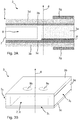
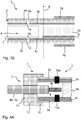
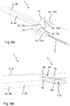
- FIGS. 1A, 1B . 2A and 2B Various embodiments of the cable assembly 2 are inter alia in the FIGS. 1A, 1B . 2A and 2B whereas different embodiments of the plate assembly 3 are shown in FIGS FIGS. 3A to 3E are shown.
- the Figures 1A and 1B show various embodiments of the cable assembly 2.
- This comprises at least a first cable 2a, 2b, 2c, 2d.
- the first cable 2a is preferably shielded, on the one hand to increase the immunity to interference and, on the other hand, to reduce the emission of interference.
- the (shielded) first cable 2a of the cable assembly 2 is shown in the form of a coaxial line.
- This comprises an inner conductor 4a, which consists of an electrically conductive material such as copper or comprises such a material.
- the inner conductor 4a of the first cable 2a is surrounded by a dielectric 4b, which consists of an electrical insulator, in particular a (elastic) Plastic exists.
- the dielectric 4b may optionally be surrounded by a shielding film 4c, which preferably comprises a dielectric material, in particular a plastic film (eg PET film), on which a metal has been vapor-deposited or sputtered on.
- the layer thickness of this metal which may be, for example, aluminum, is preferably 10 .mu.m to 20 .mu.m.
- External conductor 4d is still applied to this optional screen foil 4c.
- each of these cables 2a, 2b, 2c, 2d comprises at least the inner conductor 4a, the dielectric 4b surrounding the inner conductor 4a, the outer conductor 4d and an outer jacket 4e.
- the cable assembly 2 off Figure 1A may also include an unshielded twisted pair (UTP) cable.
- UTP unshielded twisted pair
- the shield foil 4c and the outer conductor 4d are omitted, and the outer shell 4e is merely optionally provided.
- the cable can also be connected via a UTP single core.
- cables 2a, 2b, 2c, 2d can share the screen foil 4c, the outer conductor 4d and the outer sheath 4e.
- Such a structure of the cable assembly 2 is in FIG. 1B shown.
- FIG. 1B shows a cable assembly 2 with multiple cables 2a, 2b, which form a HSD cable.
- the cable assembly 2 off FIG. 1B may also be a Shielded Twisted Pair (STP) cable or a Shielded Parallel Pair (SPP) cable or a Shielded Parallel Quad (SPQ) cable.
- STP Shielded Twisted Pair
- SPP Shielded Parallel Pair
- SPQ Shielded Parallel Quad
- the inner conductors 4a are not twisted ("twisted") under the shielding film 4c, but parallel to each other.
- the cable assembly 2 is therefore not limited to a coaxial cable or an HSD cable.
- Each of these cables 2a, 2b comprises an inner conductor 4a and a dielectric 4b surrounding the inner conductor 4a.
- an (optional) common shielding foil 4c surrounds the dielectrics 4b of both cables 2a, 2b.
- a common outer conductor 4d is wound, which in turn is surrounded by a common outer jacket 4e.
- LVDS Low Voltage Differential Signaling
- the cable 2a, 2b, 2c, 2d could also comprise only the inner conductor 4a and the outer jacket 4e, which surrounds the inner conductor 4a.
- a cable arrangement 2 with one or more cables 2a, 2b, 2c, 2d is connected as fully automatically as possible to a panel arrangement 3 can be.
- certain layers of the cables 2a, 2b, 2c, 2d must be exposed, which electrically contact different terminal regions of the plate assembly 3.
- FIG. 2A shows a cable 2a, 2b, 2c, 2d of the cable assembly 2 in the form of a coaxial cable, as this already in terms of its construction in Figure 1A has been described, to which reference is hereby made.
- at least individual layers 4a, 4b, 4c, 4d, 4e are cut to a different length and pulled off.
- at least the inner conductor 4a, the dielectric 4b and the outer conductor 4d come to light with its shield wire mesh.
- the shield wires of the outer conductor 4d are turned backwards, ie away from the exposed inner conductor 4a, ie folded back or folded over and optionally shortened (eg by means of a laser or a knife).
- the dielectric 4b also protrudes by a certain length from the outer conductor 4d. The same applies to the inner conductor 4a with respect to the dielectric 4b.
- a screen foil 4c is not present or already completely removed.
- FIG. 2B is still a metal foil 5 shown, which surrounds the outer conductor 4d and thus in particular the braid or the majority of the exposed screen braid of the outer conductor 4d or wound around it.
- This metal foil 5 ensures that the individual screen wires remain stationary during the production of the connection connection 1 and also thereafter and no unwanted electrical contact takes place (for example, to the inner conductor 4a of a cable 2a, 2b, 2c, 2d).
- the inner conductor 4a of at least one cable 2a, 2b, 2c, 2d consists of a stranded wire, wherein the individual wires of this strand are preferably soldered together in a solder bath, so that they do not protrude from the remaining wires forming the actual inner conductor 4a and unwanted trigger electrical contacts.
- connection connection 1 the cable arrangement 2 is connected to the plate arrangement 3.
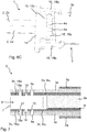
- a simplified (longitudinal) sectional view through the plate assembly 3 is for example the FIGS. 3A and 3E refer to.
- the plate arrangement 3 is, in particular, a printed circuit board or printed circuit board on which circuit carriers in the form of chips are arranged, in particular soldered.
- the plate arrangement 3 preferably comprises at least two metal layers, which means that conductor tracks or the circuit carriers extend or can be mounted on both sides of the printed circuit board.
- the plate assembly 3 comprises at least three layers 3a, 3b, 3c stacked on one another in the longitudinal direction 6.
- An intermediate layer 3a is arranged between a first outer layer 3b and a second outer layer 3c. All three layers 3a, 3b, 3c are directly or indirectly connected to each other, so in particular glued and / or pressed.
- the intermediate layer 3a may also be referred to as a laminate core and consists for example of FR4.
- the intermediate layer 3a is consequently a dielectric, wherein, depending on the desired data rate, a suitable dielectric with corresponding dielectric losses is used.
- the thickness (extension in the longitudinal direction 6) of the intermediate layer 3a substantially corresponds to the diameter of the inner conductor 4a of the at least one cable 2a to 2d.
- the wording "approximately” is to be understood to mean that the diameter of the inner conductor 4a is preferably less than 40%, 30%, 20%, 10% smaller than the thickness of the intermediate layer 3a.
- the thickness of the intermediate layer 3a is preferably less than 3mm, 2mm, 1mm, 0.7mm, 0.6mm, 0.5mm. Depending on the diameter of the inner conductor 4a, the thickness of the intermediate layer 3a can be selected accordingly.
- the first outer layer 3b is preferably made of copper with a thickness of 18 ⁇ m to 35 ⁇ m.
- both the first and the second outer layer 3b, 3c are electrically conductive. This would not necessarily be the case. It would be sufficient if an outer layer 3b, 3c would be electrically conductive. As will be explained later, although both outer layers 3b, 3c are electrically conductive, however, these are divided into different terminal areas, which in turn are not electrically connected to each other.
- the wording "position" in this context means only one layer, wherein this layer along the plate assembly 3 does not have to be contiguous and in particular does not have to be at the same electrical potential.
- the plate assembly 3 still comprises a first and second cover layer 3d, 3e.
- This first and second cover layer is preferably a (flexible) solder stop layer. This prevents the solder from being distributed outside of certain connection pads 3g when soldering various electrical components (for example circuit carriers).
- the liquid solder, with which the electrical components are soldered to corresponding connection pads 3g, does not come to rest on the first or second cover layer 3d, 3e.
- the connection pads 3g may be located on the first and second cover layers 3d, 3e.
- FIGS. 3A and 3E there is another inner layer 3f.
- This further inner layer 3f is arranged between the intermediate layer 3a and the second outer layer 3c.
- the second outer layer 3c is therefore only indirectly and not directly or directly connected to the intermediate layer 3a.
- the further inner layer 3f is, for example, a layer of polyimide.
- This layer preferably has a layer thickness of 20 .mu.m to 50 .mu.m.
- the drawn layer thicknesses are chosen only by way of example. In reality, the intermediate layer 3a will have the greatest thickness.
- the thickness of the intermediate layer 3a is preferably greater than the first and / or second outer layer 3b, 3c alone or larger than both outer layers 3b, 3c together.
- the layer thickness of the intermediate layer 3a is greater than the layer thicknesses of all other layers 3b to 3f together.
- the plate assembly 3 comprises between the first outer layer 3b and the second outer layer 3c still a recess 7, which in FIG. 3A is shown in dashed lines.
- This recess 7 defines a cable receiving space 8, which is formed on a first side edge 3 1 of the plate assembly 3.
- parts of the cables 2a to 2d, in particular their exposed inner conductors 4a and, in addition, their outer conductors 4d, are introduced into this cable receiving space 8.
- This cable receiving space 8 is therefore accessible from outside the disk assembly 3 when no terminal connection 1 between the cable assembly 2 and the disk assembly 3 is made by inserting the individual cables 2a to 2d into the cable receiving space 8.
- the recess 7 is preferably formed by a machining process, in particular a milling and / or drilling process at least in the intermediate layer 3a. It would also be possible for the recess 7 to be formed by using less material for the intermediate layer 3a or the further inner layer 3f merely when assembling the individual layers 3a to 3f, as a result of which the first and second outer layers 3b, 3c overlap Intermediate layer 3a on the first side edge 3 1 survive. In this case, no milling and / or drilling process would be needed. Parts of the intermediate layer 3a or the inner layer 3f could also be punched out or cut away before the gluing and / or pressing of the plate arrangement 3.
- the recess 7 of the plate assembly 3 is accessible through the cable assembly 2 only from the side of the plate assembly 3 and not from above or below. This means that the recess 7 is accessible only with a motion vector which runs parallel or with a component predominantly parallel to the individual layers 3a to 3f.
- FIG. 3E shows in contrast to FIG. 3A nor at least a first mecanicleiternessierö réelle 9a, which passes through the first outer layer 3a and the second outer layer 3b and opens into the cable receiving space 8.
- the at least one first inner conductor contact opening 9a preferably passes through both outer layers 3b, 3c.
- the inner conductor contact opening 9a is preferably a VIA (Vertical Interconnect Access).
- the inner conductor contact opening 9a therefore preferably runs perpendicular to the individual layers 3a to 3f, ie parallel to the longitudinal direction 6.
- An inner wall 10 of the first êtleiternessierö réelle 9a is preferably galvanized with a metal layer.
- this first inner conductor contact opening 9a penetrates only the two outer layers 3b, 3c and the two cover layers 3d, 3e.
- the intermediate layer 3a also delimits the recess 7 along the longitudinal direction 6 and has not been completely removed. This means that the recess 7 extends only over part of the entire thickness of the intermediate layer 3a, whereby the intermediate layer 3a comprises two spaced-apart regions 11a, 11b which run parallel to the outer layers 3b, 3c.
- the first region 11a is arranged on the first outer layer 3b and the second region 11b on the second outer layer 3c.
- the inner wall 10 is galvanized, so electrically conductive.
- the diameter of the at least one inner conductor contact opening 9a is preferably smaller than the diameter of the inner conductor 4a of a cable 2a to 2d.
- the first venezleiternessierö réelle 9 a is preferably located closer to the rear end of the receiving space 7 than at the front end of the receiving space 7, wherein the front end of the receiving space 7 on the first side edge 3 1 is or begins.
- the at least one first inner conductor contact opening 9a could also be arranged in the middle or in the first half (closer to the first side edge 3 1 ) relative to the length of the receiving space 7.
- FIGS. 3B to 3D show various exemplary spatial configurations of the plate assembly 3.
- a first mecanicleiternessierö réelle 9a in the FIG. 3B is introduced only in the first outer layer 3b, there is still at least a second mecanicleiternessierö réelle 9b.
- this corresponds to that structure of the at least one first inner conductor contact opening 9a.
- FIG. 3B only three layers 3a, 3b, 3c are shown, whereas the Figures 3C and 3D show a spatial structure, the sectional representation of the FIG. 3E can be seen (exception: connection pads 3g).
- FIG. 3B the recess 7 was milled or drilled.
- the recess 7 could have been punched or cut out of the intermediate layer 3a before the plate assembly 3 was produced by a stamping process.
- FIG. 3B is the recess 7 only accessible via the first side edge 3 1 from the outside.
- a second side edge 3 2 and a third side edge 3 3 of the plate assembly 3 extend to the first side edge 3 1 and form with this in each case an angle of preferably 90 ° (deviations of less than 40 °, 30 °, 20 °, 15 °, 10 °, 5 ° are included).
- the second and the third side edge 3 2 , 3 3 are in FIG. 3B inaccessible from the outside, so closed.
- the situation is different with the Figures 3C and 3D out.
- the receiving space 7 of the second and third side edge 3 2 , 3 3 also accessible.
- the inner conductor contact openings 9a, 9b do not count as access to the receiving space 7.
- the plate arrangement 3 according to FIGS Figures 3C and 3D can be produced by a machining process, wherein the cutting tool used with a corresponding Vorstelltiefe corresponding to the depth (length) of the receiving space, from the second side edge 3 2 in the direction of the third side edge 3 3 is moved at the level of the intermediate layer 3a. This method can still be done in several step-like paragraphs, ie in several different depths.
- the plate assembly 3 could according to the Figures 3C and 3D also be produced in a stamping process, wherein prior to production of the plate assembly 3, a part of the intermediate layer 3a is punched or cut and removed. In principle, simply less material could also be used for the intermediate layer 3a than for the further layers 3b, 3c or 3d, 3e.
- the plate assembly 3 has a thickness which is preferably less than 15mm, 13mm, 1mm, 9mm, 8mm, 7mm, 6mm, 5mm, 4mm, 3mm, 2mm and further preferably greater than 1mm, 2mm, 3mm, 4mm, 5mm , 6mm, 7mm, 8mm, 9mm, 10mm.
- the depth (length) of the cable receiving space 8, so starting from the first side edge 3 1 to the fully assembled intermediate layer 3a is preferably less than 20mm, 18mm, 16mm, 14mm, 12mm, 10mm, 8mm, 6mm and is preferably greater than 5mm, 7mm, 9mm, 11mm, 13mm, 15mm, 17mm, 19mm.
- the width of the recess ie from the open second end 3 2 towards the open third end 3 3 , for example, preferably less than 50 mm, 40 mm, 30 mm, 26 mm, 22 mm, 18 mm, 14 mm, 10 mm, 6 mm and is preferably greater than 8 mm, 12 mm, 16 mm, 20mm, 24mm, 28mm, 35mm, 45mm.
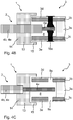
- FIGS. 4A to 4E show different ways how the inventive connection connection 1 is produced.
- the FIGS. 4A to 4D show in each case an at least partially cut (longitudinal section) representation through the inventive connection connection 1 with the cable assembly 2 and the plate assembly 3rd Figure 4E on the other hand shows a plan view of the connection connection 1 according to the invention, wherein the first and second outer layer 3b, 3c of the plate assembly 3 is not shown.
- the cable assembly 2 comprises in the FIGS. 4A to 4E only a first cable 2a with the inner conductor 4a and the dielectric 4b and the outer sheath 4e.
- the at least one first cable 2a does not comprise an outer conductor 4d. It is also shown that the at least one first inner conductor contact opening 9a is provided with at least one first inner conductor solder deposit 12a.
- the distance between the inner conductor 4a and the at least one first mecanicleiternessierö réelle 9a is not shown to scale in the drawing figures.
- the inner conductor 4a is in reality only minimally (preferably less than 3mm, 2mm, 1mm) spaced from the first and / or second outer layer 3b, 3c.
- the inner conductor 4a is spaced apart with its front side, that is arranged without contact to a front side of the intermediate layer 3a.
- the at least one first cable 2a of the cable arrangement 2 is inserted into the cable receiving space 8 via the recess 7 which is open towards the first side edge 3 1 .
- the at least one first cable 2a is thereby introduced into the cable receiving space 8 with a motion vector which runs parallel or predominantly parallel to the first and / or second outer layer 3b, 3c or to the intermediate layer 3a.
- the at least one first cable 2 a ends with its inner conductor 4 a in the cable receiving space 8 and does not stand with the end of the exposed inner conductor 4 a out of the cable receiving space 8.
- the cable arrangement 2 also comprises a cable collection and alignment device 13, which has a main body 14.
- the cable collection and alignment device 13 is preferably arranged immovably on the at least one first cable 2a or on all cables 2a to 2d.
- the cable collection and alignment device 13 is arranged on the dielectric 4b or outer sheath 4e.
- the cable collection and alignment device 13 can also enclose the inner conductor 4a.
- the cable collection and alignment device 13 is made of a dielectric material, for example of a plastic. It may comprise a plastic housing, in which the at least one first cable 2a is inserted, after which the plastic housing is firmly closed. Preferably, however, the at least one first cable 2a is encapsulated with a plastic, whereby the cable collecting and aligning device 13 is formed.
- the cable collecting and aligning device 13 also comprises a fastening device 15 which is designed to fix the cable collection and alignment device 13 to the plate assembly 3 such that the at least one first cable 2a or all cables 2a to 2d the cable assembly 2 are arranged immutable to one another in the cable receiving space 8 inserted and in the cable receiving space 8 are arranged immutable to each other.
- the fastening device 15 is configured total thread or screw free and solderless.
- the at least one first cable 2a or all cables 2a to 2d are guided through the main body 14 of the cable collection and alignment device 13.
- the main body 14 includes, for example, a rectangular longitudinal section or is cuboid.
- FIG. 4B is the connection 1 completely made.
- the first inner conductor solder deposit 12a has been heated until it has become molten and has produced a first inner conductor solder connection 16a via which the inner conductor 4a has the at least one first cable 2a at least in the region of the first inner conductor contact opening 9a with a first inner conductor connection region 9a 1 of the first and / or second outer layer 3b , 3c is soldered electrically conductive.
- the term outer layer 3b, 3c is understood to mean the entire electrically conductive metal layer, wherein this metal layer is in different, mutually galvanically isolated connection areas (eg first inner conductor connection area 9a 1 ) is divided.
- the first inner conductor solder deposit 12a can be made molten by means of a heated tip of a soldering iron or a soldering device. Preferably, however, an inductive (non-contact) soldering method is used.
- the at least one first inner conductor solder deposit 12a could also be arranged in the form of a solder ring or a soldering sleeve on the inner conductor 4a of the at least one first cable 2a.
- Figure 4D also shows that the recess 7 is introduced only in the intermediate layer 3a, but does not extend over the entire thickness of the intermediate layer 3a.
- the intermediate layer 3a is thereby divided into spaced-apart regions 11a, 11b, which extend in the direction of the first side edge 3 1 .
- the first inner conductor contact opening 9a passes through both regions 11a, 11b of the intermediate layer 3a.
- An electrical contacting of the inner conductor 4a with the first inner conductor connection region 9a 1 of the first and / or second outer layer 3b, 3c takes place via the inner wall 10 of the êtleiternessierötechnisch 9a.
- This inner wall 10 is in particular galvanized with a metal layer.
- FIG 4E is a plan view of the connection connection 1 shown.
- the first and / or second outer layer 3b, 3c is not shown.
- the first inner conductor contact opening 9a is indicated, which is enlarged in diameter.
- the diameter of the first inner conductor contacting opening 9a is preferably smaller than the diameter of the inner conductor 4a.
- the inner conductor 4a of the at least one first cable 2a is, as in FIG Figure 4E represented at the first side edge 3 1 inserted into the cable receiving space 8 and arranged in plan view of the first and / or second outer layer 3b, 3c under the at least one first mecanicleiterfulnessierö réelle 9a.
- fastening device 15 which prevents detachment or removal of the cable assembly 2 from the plate assembly 3 and provides strain relief of the at least one first cable 2a, so that the first Certainlyleiterlöttagen 16a is not affected.
- the type of fastening device 15 shown here will be described in more detail with regard to the later embodiments.
- FIG. 4F shows that the cable assembly 2 still comprises at least a second cable 2b. It is shown that the second cable 2b comprises an inner conductor 4a and a dielectric 4b or an outer jacket 4e. An outer conductor 4d is not provided here.
- the cables 2a, 2b of the cable assembly 2 are arranged side by side. They are preferably at least with respect to their exposed inner conductor 4a in a common plane, said common plane in turn runs parallel to the plate assembly 3 and parallel to the individual layers 3a to 3f.
- the inner conductors 4a of the two cables 2a, 2b are galvanically separated from each other and arranged without contact to each other.
- a second reterciskingierö réelle 9b is provided, which is constructed as the first mecanicleiternessierö réelle 9a.
- the second reteleiternessierö réelle also passes through the first and / or the second outer layer 3b, 3c and opens into the cable receiving space 8.
- the inner conductor 4a of at least one second cable 2b is inserted at the first side edge 3 1 in the cable receiving space 8 and in plan view of the first or second outer layer 3b, 3c arranged under the at least one second reteleiternessierö réelle 9b.
- the inner conductor 4a of the at least one second cable 2b is connected via a second mecanicleiterlötvig (not shown) at least in the region of the second mecanicleiternessierö réelle 9b with a second inner conductor terminal region 9b 1 (see FIG. FIG. 6B ) of the first and / or second outer layer 3b, 3c electrically conductively soldered.
- the first inner conductor connection region 9a 1 and the second inner conductor connection region 9b 1 are galvanically separated from one another.
- the fastening device 15 of the cable collection and alignment device 13 also comprises a plurality of separating webs 15a, which extend from the at least one base body 14 in the direction of the plate assembly 3 and terminate in the cable receiving space 8.
- the dividers 15a are also made of a dielectric material.
- the cable collection and alignment device 13 is formed integrally with its fastening device 15 and the main body 14 and in particular produced in a plastic injection molding process.
- the dividing webs 15a extend in the same direction as the inner conductors 4a of the two cables 2a, 2b.
- the separating webs 15a preferably project beyond the end faces, that is to say the ends of the inner conductors 4a. This means that when inserting the cable assembly 2, ie the inner conductor 4a and the separating webs 15a, in the cable receiving space 8, the dividing webs 15a can first reach with their end faces in a stop position with the intermediate layer 3a.
- the partitions 15a therefore flank the inner conductors 4a of the cables 2a, 2b.
- Each inner conductor 4a is preferably surrounded by at least two separating webs 15a.
- the separating webs 15 a have a thickness which is smaller than the thickness of the recess 7.
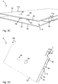
- FIG. 5 shows a spatial representation of the cable collection and alignment device 13 of the cable assembly 2.
- the dividers 15a of the fastening device 15 have already been explained.
- the individual dividers 15a can be different widths, with their thickness is preferably the same.
- the outer two separating webs 15a are wider than the middle separating web 15a.
- the dividers 15a are flattened from all sides in the direction of their free-standing end to facilitate insertion into the receiving space 7.
- the fastening device 15 additionally comprises a first latching hook 15b 1 and a second latching hook 15b 2 .
- the latching hooks 15b 1 , 15b 2 originate at different areas of the main body 14, in particular at different ends of the main body 14 (but preferably on the same side of the main body 14) and extend in the direction of the second and third side edges 3 2 and 3 3 of the plate assembly 3.
- a first detent opening 17a and a second detent opening 17b can be seen.
- the first latching opening 17a is formed on the second side edge 3 2 and the second latching opening 17b on the third side edge 3 3 .
- the latching openings 17a, 17b preferably pass through all the layers 3a to 3f of the plate arrangement 3.
- the latching openings 17a, 17b can be introduced into the plate arrangement 3, for example, after the plate assembly 3 has been produced. However, they could already be introduced in the individual layers 3a to 3f, ie even before the individual layers 3a to 3f are glued and / or pressed to the plate arrangement 3.
- the latching openings 17a, 17b are therefore accessible not only from the second and third side edge 3 2 , 3 3 , but also in a plan view of the first and second outer layer 3b, 3c.
- the latching openings 17a, 17b preferably have a cube-shaped volume.
- the first latching hook 15b 1 engages in the first latching opening 17a and the second latching hook 15b 2 in the second latching opening 17b.
- the latching hooks 15b 1 , 15b 2 engage behind a support shoulder formed by the engagement opening 17a, 17b in the plate arrangement 3.
- the latching hooks 15b 1 , 15b 2 are resilient. They should at least be able to move towards and away from each other.
- the front part of the latching hook 15b 1 , 15b 2 is preferably L-shaped and further preferably at least partially obliquely or conically enlarged in the direction of the base body 14, so that when making the connection connection 1, ie when inserting the cable assembly 2 in the plate assembly 3, the latching hooks 15b 1 , 15b 2 are pressed away from each other until the front hook portion of the individual latching hooks 15b 1 , 15b 2 engages in the corresponding latching opening 17a, 17b.
- the latching hooks 15b 1 , 15b 2 have a thickness which corresponds approximately to that of the plate assembly 3. However, the thickness can also be smaller or larger.
- the latching hooks 15b 1 , 15b 2 along the longitudinal direction 6 are less resilient than along the direction of movement, in which the latching hooks are moved toward or away from each other.
- the fastening device 15 additionally comprises a first and a second fastening tongue 15c 1 , 15c 2 .
- the two fastening tongues 15c 1 , 15c 2 extend away from the base body 14 in the direction of the plate arrangement 3.
- the plate assembly 3 is arranged with its first side wall 3 1 between the two fastening tongues 15c 1 , 15c 2 . This means that the first fastening tongue 15c 1 rests on the first outer layer 3b and the second fastening tongue 15c 2 rests on the second outer layer 3c.
- the fastening tongues 15c 1 , 15c 2 preferably extend less far in the direction of the plate arrangement 3 than the latching hooks 15b 1 , 15b 2 .
- the fastening tongues 15c 1 , 15c 2 also extend less far in the direction of the plate assembly 3 than the separating webs 15 a.
- the fastening tongues 15c 1 , 15c 2 do not cover the first or second or the further inner conductor contact openings 9a, 9b, 9c, 9d.
- the fastening tongues 15c 1 , 15c 2 in particular also do not cover the first or second or the further outer conductor contact openings 18a, 18b, 18c, 18d, which will be explained later.
- the fastening tongues 15c 1 , 15c 2 extend over the predominant part (more than 50%) of the length of the basic body 14.
- the separating webs 15a, the latching hooks 15b 1 , 15b 2 and the fixing tongues 15c 1 , 15c 2 all run in the same direction.
- the fastening device 15 also comprises at least two fastening pins 15d (FIG. FIG. 6A ) passing through the two fixing tongues 15c 1 , 15c 2 and the plate assembly 3 and in this particular by the first and second outer layer 3b, 3c, whereby a peeling of the cable assembly. 2 is prevented by the plate assembly 3.
- the fastening pins 15d are preferably pressed in. An adhesion of the fastening tongues 15c 1 , 15c 2 with the outer layers 3b, 3c instead of the fastening pins 15d could also be possible.
- the fastening tongues 15c 1 , 15c 2 are the preferred fastening means of the fastening device 15, because the use of the latching hooks 15b 1 , 15b 2 requires that the plate arrangement 3 has a precisely defined width.
- the plate assembly may have any width.
- a ball catch below the respective fastening tongue 15c 1 , 15c 2 can also be used.
- a projection, in particular in the form of a sphere, would protrude from both fastening tongues 15c 1 , 15c 2 in the direction of the first and second outer layer 3b, 3c, ie in the longitudinal direction 6, into a corresponding receiving opening at least in the first and second outer layer 3b, 3c intervene.
- this type of attachment is not as effective as with the mounting pins 15d, but cheaper to manufacture.
- FIGS. 6A and 6C show the use of the cable collection and alignment device 13.
- the connection connection 1 is made.
- the cable assembly 2 in the FIG. 6A two cables 2a, 2b, on which the cable collection and alignment device 13 is arranged immovably (in the mounted state).
- the cables 2a, 2b pass through the base body 14.
- the fastening device 15 of the cable collection and alignment device 13 engages at different locations in the plate assembly 3, so that a strain relief is made possible, whereby no damage to the réelleleiterlöttagen 16a takes place even when pulling on the cables 2a, 2b.
- FIG. 6B is a view into the open receiving space 7 shown, where it can be seen how the inner conductors 4a of the cables 2a, 2b are disposed in the cable receiving space 8 below the respective réelleleiter gleichierö réelleen 9a, 9b.
- FIGS. 7 and 8A to 8D show a further embodiment of the connection connection 1 according to the invention, in which the at least one first cable 2a is soldered both with its inner conductor 4a and with its outer conductor 4d with the plate assembly 3.
- FIG. 7 shows a simplified sectional view through a corresponding plate assembly 3.
- the plate assembly 3 also includes a first outer conductor contacting opening 18a, which passes through the first outer layer 3b and / or the second outer layer 3c and opens into the cable receiving space 8.
- the first outer conductor contacting opening 18a preferably corresponds to the first inner conductor contacting opening 9a with respect to its construction and its manufacture.
- the outer conductor contacting opening 18a is arranged closer to the first side edge 3 1 than the first inner conductor contacting opening 9a.
- An inner wall 21 of the first outer conductor contacting opening 18a is preferably galvanized with a metal layer.
- first outer layer 3b and the second outer layer 3c have different hatchings. These different hatchings are intended to make clear that the first outer layer 3b and the second outer layer 3c comprise different connection regions 9a 1 , 18a 1 .
- first outer layer 3b and the second outer layer 3c comprise different connection regions 9a 1 , 18a 1 .
- Both terminal areas 9a 1 , 18a 1 are galvanically separated from each other by an interruption 19. However, they are preferably formed from the same metal substrate. This means that the first inner conductor connection region 9a 1 is galvanically isolated from the first outer conductor connection region 18a 1 .
- This interruption 19 can be introduced in the construction of the first and / or the second outer layer 3b, 3c by a lack of construction of the metal layer or the metal layer can be removed in a subsequent etching and / or milling process, whereby the interruption 19 is formed.
- the inner conductor connection region 9a 1 is preferably formed by a signal line, whereas the outer conductor connection region 18a 1 is formed by a ground surface that is wider than the signal line.
- a first cable 2a which comprises the inner conductor 4a, a dielectric 4b surrounding the inner conductor 4a, an outer conductor 4d and an outer conductor jacket 4e surrounding the outer conductor.
- the outer conductor jacket 4e and the dielectric 4d are not electrically conductive.
- the outer conductor 4d comprises a screen wire mesh, the shield wires are folded back or folded down in the inserted state in the direction of the first side edge 3 1 , as with respect to the FIGS. 2A and 2B has been described.
- a metal foil 5 is applied, which ensures that the shield wires remain in place.
- This electrically conductive metal foil 5 can also be referred to as a soldering aid.
- the at least one first cable 2a in this case is a coaxial cable.
- the braided screen is preferably everted away from the end of the at least one first cable 2a introduced into the cable receiving space 8 to the rear.
- the outer conductor 4d of the at least one first cable 2a is at least partially or predominantly inserted with respect to its length at the first side edge 3 1 in the cable receiving space 8.
- the outer conductor 4d is arranged under the at least one outer conductor contact opening 18a.
- the inner conductor 4a is arranged under the at least one first inner conductor contact opening 9a.
- At least one first outer conductor solder deposit 22a is also shown.
- the at least one first outer conductor solder deposit 22a is preferably introduced into the outer conductor contact opening 18a. It could also be arranged on the outer conductor 4d.
- the outer conductor solder connection 20a must nevertheless be made in the first outer conductor connection region 18a 1 .
- the first takes place Outer conductor solder joint less than 10mm, 8mm, 5mm apart from the first outer conductor contact hole 18a.
- isseleiterlötvig 16a which is arranged "in the area" of the first mecanicleiternessierö réelle 9a.
- the different regions 11a, 11b of the intermediate layer 3a have a different thickness along the cable insertion direction.
- the two regions 11a, 11b are thicker than in that region of the cable connection space 8 in which the outer conductor 4d of the at least one first Cable 2a is to be soldered.
- FIG 8D shows a plan view of the connection connection 1 according to the invention, the at least four cables 2 a to 2 d contacted with corresponding connection areas 9 a 1 , 18 a 1 and 9 b 1 .
- Each cable 2a to 2d is designed as a coaxial cable.
- the outer sheath 4e of all cables 2a to 2d is held by the cable-collecting and aligning device 13.
- Dividers 15a are arranged between the exposed outer conductors 4d and the exposed inner conductors 4a.
- the cable arrangement 2 can be manufactured completely before the connection connection 1 is produced.
- the individual layers of the cables 2a to 2d are already exposed in advance or assembled and fixed by the corresponding cable collection and alignment 13 rotationally fixed and immutable to each other.
- Such a prepared cable assembly 2 can be easily inserted into the cable receiving space 8.
- the separating webs 15a result in the inner conductors 4a not coming into contact with the individual layers 3a to 3f of the cable receiving space 8.
- the inner conductor contact holes 9a to 9d and 18a to 18d, respectively, into which the respective inner conductor solder deposits 12a, 22a are inserted, can be molten via an external heat source located outside the plate assembly 3 in particular are made, whereby the individual cables 2a to 2d with the respective terminal portions 9a 1 and 18a 1 are soldered.
- any number of cables 2a to 2d can be arranged side by side.
- two cables 2a, 2b can be arranged one above the other, with the inner conductor 4a of one cable 2a being soldered to the first outer layer 3b and the inner conductor 4a of the second cable 2b to the second outer layer 3c.
- this requires a correspondingly thick intermediate layer 3a.
- the individual outer conductor contact regions 18a 1 of all cables 2a to 2d can be connected to one another in an electrically conductive manner. This is not the case with the inner conductor contacting regions 9a 1 , 9b 1 .
- a cable 2 a to 2 d could also be used, which according to FIG. 1B is constructed.
- a common outer conductor 4d would be used, which jointly surrounds the dielectrics 4b with the respective inner conductors 4a of different cables 2a to 2d.
- Such a cable 2a to 2d would no longer have a round cross-section, but could comprise cross-sectionally different sides.
- connection connection 1 and the plate assembly 3 part of the invention. This applies in particular if the first inner conductor contact opening 9a has at least one first inner conductor solder deposit 12a.
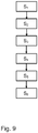
- FIG. 9 shows a method for producing the connection connection 1 between the plate assembly 3 and the cable assembly 2.
- the plate assembly 3 is prepared. This comprises at least three layers 3a, 3b, 3c stacked on one another in the longitudinal direction 6.
- at least the dielectric intermediate layer 3a is arranged between a first outer layer 3b and a second outer layer 3c.
- the first and / or second outer layer 3b, 3c are in particular metal layers (eg copper).
- a recess 7 is introduced between the first outer layer 3b and the second outer layer 3c. This results in a cable receiving space 8, which is accessible from the first side edge 3 1 of the plate assembly 3 from.
- a second method step S 2 at least one first mecanicleiternessierö réelle 9 a is introduced into the plate assembly 3, which passes through the first outer layer 3 b and / or the second outer layer 3 c and opens into the cable receiving space 8.
- the at least one first inner conductor contact opening 9a is, in particular, a through-connection which extends equally through both outer layers 3b, 3c. This via can be made for example in a drilling process. Galvanization of the inner wall 10 of the first réelleleiternessierö réelle 9 a is also possible.
- a third method step S 3 at least the inner conductor 4 a of the at least one first cable 2 a of the cable arrangement 2 is exposed.
- this method step can also be carried out before the first or second method step S 1 , S 2 .
- a fourth method step S 4 at least one inner conductor solder deposit 12a is introduced or applied into the inner conductor contact opening 9a and / or to the exposed inner conductor 4a of the at least one first cable 2a of the cable arrangement 2.
- a fifth method step S 5 the inner conductor 4 a of the at least one first cable 2 a is inserted into the cable receiving space 8 via the first side edge 3 1 , so that the inner conductor 4 a of the at least one first cable 2 a is in top view of the first or second outer layer 3 b, 3 c that is, arranged along the longitudinal direction 6 under the at least one first inner conductor contact opening 9a.
- a sixth method step S 6 the inner conductor solder deposit 12a is heated until it is molten and the inner conductor 4a of the at least one first cable 2a via a first mecanicleiterlötvig 16a at least in the region of the first mecanicleiternessierö réelle 9a with a first inner conductor connection region 9a 1 of the first and / or second outer layer 3b, 3c electrically conductively connects.
- connection connection 1 can be introduced into a housing which consists for example of plastic or comprises such or which is electrically conductive to the To reduce interference emission of the connection 1 and to increase immunity to interference.
- the connection connection 1 is used in particular for the center console in vehicles to transmit, for example, screen signals or USB signals to a display attached there or a connector or to receive from there.
- a vehicle is a motor vehicle, such as a car, truck, but also a train, an airplane or a ship.
- a user may attach a USB data carrier to the connector.
- at least one computer chip which supports the production of the USB connection is preferably located on the plate arrangement 3.
- the connector could also be used to charge a user's mobile terminal.
- at least one charging current (direct current or alternating current) would be transmitted via the inner conductor 4a of the at least one first cable 2a.
Landscapes
- Engineering & Computer Science (AREA)
- Manufacturing & Machinery (AREA)
- Microelectronics & Electronic Packaging (AREA)
- Coupling Device And Connection With Printed Circuit (AREA)
- Multi-Conductor Connections (AREA)
- Manufacturing Of Electrical Connectors (AREA)
Claims (15)
- Raccord de connexion (1), pourvu d'un ensemble de câbles (2) et d'un ensemble de plaques (3), présentant les caractéristiques suivantes :- l'ensemble de plaques (3) comprend au moins trois couches (3a, 3b, 3c) empilées les unes sur les autres dans la direction longitudinale (6), une couche intermédiaire (3a) étant placée entre une première couche extérieure (3b) et une deuxième couche extérieure (3c) et toutes les trois couches (3a, 3b, 3c) étant assemblées directement ou indirectement les unes aux autres ;- la première couche extérieure (3b) et/ou la deuxième couche extérieure (3c) est conductrice d'électricité et la couche intermédiaire (3a) comprend une matière diélectrique ;- l'ensemble de plaques (3) comprend entre la première couche extérieure (3b) et la deuxième couche extérieure (3c) un évidement (7), par lequel est créé un espace de logement de câbles (8) sur un premier bord latéral (31) de l'ensemble de plaques (3) ;- au moins un premier orifice de contact d'un conducteur interne (9a) traverse la première couche extérieure (3b) et/ou la deuxième couche extérieure (3c) et débouche dans l'espace de logement de câbles (8) ;- l'ensemble de câbles (2) comprend au moins un premier câble (2a), le premier câble (2a) comportant un conducteur interne (4a) ;- le conducteur interne (4a) de l'au moins un premier câble (2a) est inséré sur le premier bord latéral (31) dans l'espace de logement de câbles (8) et placé avec un décalage en direction longitudinale (6) par rapport à l'au moins un premier orifice de contact d'un conducteur interne (9a) ;- le conducteur interne (4a) de l'au moins un premier câble (2a) est brasé de manière conductrice d'électricité par l'intermédiaire d'un premier assemblage par brasage de conducteur interne (16a), au moins dans la zone du premier orifice de contact d'un conducteur interne (9a) avec une première zone de connexion de conducteur interne (9a1) de la première et/ou deuxième couche extérieure (3b, 3c) ;caractérisé par les caractéristiques suivantes :- l'ensemble de câbles (2) comprend un système de collecte et d'alignement des câbles (13), qui est constitué d'une matière plastique ou en comprend une telle et qui comporte un corps de base (14) ;- le système de collecte et d'alignement des câbles (13) est placé de manière indéplaçable sur l'au moins un premier câble (2a) ;- le système de collecte et d'alignement des câbles (13) comprend au moins un système de fixation (15), qui est conçu sur le corps de base (14) ;- le système de fixation (15) est conçu pour fixer le système de collecte et d'alignement des câbles (13) sur l'ensemble de plaques (3), de telle sorte qu'au moins un premier câble (2a) de l'ensemble de câbles (2) soit placé de manière indéplaçable dans l'espace de logement de câbles (8).
- Raccord de connexion (1) selon la revendication 1, caractérisé par les caractéristiques suivantes :- l'évidement (7) est créé par un procédé d'enlèvement de copeaux dans la couche intermédiaire (3a) ; ou- les première et deuxième couches extérieures (3b, 3c) débordent au-delà de la couche intermédiaire (3a) sur le premier bord latéral (31), suite à quoi est créé l'évidement (7) et ainsi l'espace de connexion de câbles (8).
- Raccord de connexion (1) selon la revendication 1 ou 2, caractérisé par les caractéristiques suivantes :- l'ensemble de plaques (3) est une carte de circuit imprimé ; et- la couche intermédiaire (3a) est plus épaisse que la première et/ou la deuxième couche extérieure (3b, 3c), seules ou en commun.
- Raccord de connexion (1) selon l'une quelconque des revendications précédentes, caractérisé par la caractéristique suivante :- le premier assemblage par brasage de conducteur interne (16a) est créé sur un premier dépôt de brasure de conducteur interne (12a), le premier dépôt de brasure de conducteur interne (12a) :a) étant placé dans l'au moins un premier orifice de contact d'un conducteur interne (9a) ; et/oub) étant placé sur le conducteur interne (4a) de l'au moins un premier câble (2a), en dessous de l'au moins un premier orifice de contact d'un conducteur interne (9a).
- Raccord de connexion (1) selon l'une quelconque des revendications précédentes, caractérisé par les caractéristiques suivantes :- l'ensemble de plaques (3) comprend encore :a) une première couche de couverture (3d), qui est placée sur la première couche extérieure (3b), de telle sorte que la première couche extérieure (3b) se situe entre la couche intermédiaire (3a) et la première couche de couverture (3d), le premier orifice de contact de conducteur interne (9a) traversant la première couche de couverture (3d) ;
et/oub) une deuxième couche de couverture (3e), qui est placée sur la deuxième couche extérieure (3c), de telle sorte que la deuxième couche extérieure (3c) se situe entre la couche intermédiaire (3a) et la deuxième couche de couverture (3e), le premier orifice de contact de conducteur interne (9a) traversant la deuxième couche de couverture (3e) ;
et/ou- l'évidement (7) ne s'étend que sur une partie de l'épaisseur de la couche intermédiaire (3a), suite à quoi la couche intermédiaire (3a) comprend deux zones (11a, 11b) écartées l'une de l'autre, qui sont placées sur la première et la deuxième couche extérieure (3b, 3c) et qui délimitent l'espace de logement de câbles (8) dans la direction longitudinale (6) ;
le premier orifice de contact d'un conducteur interne (9a) traverse la première et/ou la deuxième zone (11a, 11b) de la couche intermédiaire (3a) ;
et/ou- une paroi intérieure (10) du premier orifice de contact d'un conducteur interne (9a) est galvanisée avec une couche métallique. - Raccord de connexion (1) selon l'une quelconque des revendications précédentes, caractérisé par les caractéristiques suivantes :- le premier câble (2a) de l'ensemble de câbles (2) comprend encore un conducteur externe (4d), qui est galvaniquement séparé du conducteur interne (4a) par un diélectrique (4b) ;- au moins un premier orifice de contact de conducteur externe (18a) traverse la première couche extérieure (3b) et/ou la deuxième couche extérieure (3c) et débouche dans l'espace de logement de câbles (8) ;- le premier orifice de contact de conducteur externe (18a) est placé de manière plus proche du premier bord latéral (31) que le premier orifice de contact d'un conducteur interne (9a) ;- le conducteur externe (4d) de l'au moins un premier câble (2a) est inséré sur le premier bord latéral (31) dans l'espace de logement de câbles (8) et placé en étant décalé dans la direction longitudinale (6) par rapport à l'au moins un premier orifice de contact de conducteur externe (18a) ;- le conducteur externe (4d) de l'au moins un premier câble (2a) est brasé de manière conductrice d'électricité, par l'intermédiaire d'un premier assemblage par brasage de conducteur externe (20a), au moins dans la zone du premier orifice de contact de conducteur externe (18a) avec une première zone de connexion de conducteur externe (18a1) de la première et/ou de la deuxième couche extérieure (3b, 3c) ;- la première zone de connexion de conducteur interne (9a1) est galvaniquement séparée de la première zone de connexion de conducteur externe (18a1).
- Raccord de connexion (1) selon la revendication 6, caractérisé par les caractéristiques suivantes :- le conducteur externe (4d) de l'au moins un premier câble (2a) comprend une tresse de blindage ;- l'ensemble de câbles (2) comprend au moins un premier film métallique (5) ;- le premier film métallique (5) est placé autour de la tresse de blindage.
- Raccord de connexion (1) selon l'une quelconque des revendications précédentes, caractérisé par les caractéristiques suivantes :- l'ensemble de câbles (2) comprend au moins un deuxième câble (2b) pourvu d'un conducteur interne (4a) ;- les câbles (2a, 2b) de l'ensemble de câbles (2) sont placés côte à côte ;- au moins un deuxième orifice de contact d'un conducteur interne (9b) traverse la première couche extérieure (3b) et/ou la deuxième couche extérieure (3c) et débouche dans l'espace de logement de câbles (8) ;- le conducteur interne (4a) de l'au moins un deuxième câble (2b) est inséré sur le premier bord latéral (31) dans l'espace de logement de câbles (8) et placé en décalage dans la direction longitudinale (6) par rapport à l'au moins un deuxième orifice de contact d'un conducteur interne (9b) ;- le conducteur interne (4a) de l'au moins un deuxième câble (2b) est brasé de manière conductrice d'électricité par l'intermédiaire d'un deuxième assemblage par brasage de conducteur interne, au moins dans la zone du deuxième orifice de contact d'un conducteur interne (9b) avec une deuxième zone de connexion de conducteur interne (9b1) de la première et/ou de la deuxième couche extérieure (3b, 3c) ;- la première zone de connexion de conducteur interne (9a1) et la deuxième zone de connexion de conducteur interne (9b1) sont galvaniquement séparées l'une de l'autre.
- Raccord de connexion (1) selon la revendication 8, caractérisé par les caractéristiques suivantes :- l'au moins un deuxième câble (2b) de l'ensemble de câbles (2) comprend encore un conducteur externe (4d), qui est galvaniquement séparé du conducteur interne (4a) par un diélectrique (4b) ;- au moins un deuxième orifice de contact de conducteur externe (18b) traverse la première couche extérieure (3b) et/ou la deuxième couche extérieure (3c) et débouche dans l'espace de logement de câbles (8) ;- le deuxième orifice de contact de conducteur externe (18b) est placé de manière plus proche du premier bord latéral (31) que le deuxième orifice de contact d'un conducteur interne (9b) ;- le conducteur externe (4d) de l'au moins un deuxième câble (2b) est inséré sur le premier bord latéral (31) dans l'espace de logement de câbles (8) et placé en décalage dans la direction longitudinale (6) par rapport à l'au moins un deuxième orifice de contact de conducteur externe (18b) ;- le conducteur externe (4d) de l'au moins un deuxième câble (2b) est brasé de manière conductrice d'électricité, par l'intermédiaire d'un deuxième assemblage par brasage de conducteur externe, au moins dans la zone du deuxième orifice de contact de conducteur externe (18b) avec une deuxième zone de connexion de conducteur externe de la première et/ou de la deuxième couche extérieure (3b, 3c) ;- la deuxième zone de connexion de conducteur interne (9b1) est galvaniquement séparée de la deuxième zone de connexion de conducteur externe.
- Raccord de connexion (1) selon l'une quelconque des revendications précédentes, caractérisé par les caractéristiques suivantes :- le système de fixation (13) comprend un premier et un deuxième crochet d'encliquetage (15b1, 15b2) ;- le premier et le deuxième crochet d'encliquetage (15b1, 15b2) dérivent sur différentes zones du corps de base (14) et s'écoulent dans la direction d'un deuxième et d'un troisième bord latéral (32, 33) de l'ensemble de plaques (3), le deuxième et troisième bord latéral (32, 33) de l'ensemble de plaques (3) convergeant sous un angle de 90° de préférence vers différentes extrémités du premier bord latéral (31) ;- un premier orifice d'encliquetage (17a) est conçu sur le deuxième bord latéral (32) et un deuxième orifice d'encliquetage(17b) est conçu sur le troisième bord latéral (33) ;- le premier crochet d'encliquetage (15b1) s'engage dans le premier orifice d'encliquetage (17a) et le deuxième crochet d'encliquetage (15b2) s'engage dans le deuxième orifice d'encliquetage (17b).
- Raccord de connexion (1) selon la revendication 10, caractérisé par les caractéristiques suivantes :- dans l'ensemble de plaques (3), des épaulements d'appui sont créés par les orifices d'encliquetage (17a, 17b) ;- les crochets d'encliquetage (15b1, 15b2) s'accrochent par l'arrière dans l'épaulement d'appui respectif.
- Raccord de connexion (1) selon la revendication 10 ou 11, caractérisé par la caractéristique suivante :- une partie avant des crochets d'encliquetage (15b1, 15b2) est en forme de L et s'agrandit au moins en partie en oblique ou en forme de cône dans la direction du corps de base (14).
- Raccord de connexion (1) selon l'une quelconque des revendications précédentes, caractérisé par les caractéristiques suivantes :- le système de fixation (15) comprend une première et une deuxième languette de fixation (15c1, 15c2) ;- l'ensemble de plaques (3) est placé par son premier bord latéral (31) entre les deux languettes de fixation (15c1, 15c2), la première languette de fixation (15c1) reposant sur la première couche extérieure (3b) et la deuxième languette de fixation (15c2) reposant sur la deuxième couche extérieure (3c) ;- le système de fixation (15) comprend au moins une ou au moins deux chevilles de fixation (15d), l'au moins une ou les au moins deux chevilles de fixation (15d) s'écoulant à travers les deux languettes de fixation (15c1, 15c2) et l'ensemble de plaques (3), suite à quoi, un retrait de l'ensemble de câbles (2) de l'ensemble de plaques (3) est empêché ; et/ou
entre la première languette de fixation (15c1) et la première couche extérieure (3b) est conçu un premier loqueteau à bille et/ou
entre la deuxième languette de fixation (15c2) et la deuxième couche extérieure (3c) est conçu un deuxième loqueteau à bille. - Raccord de connexion (1) selon l'une quelconque des revendications précédentes, caractérisé par les caractéristiques suivantes :- le système de fixation (15) comprend au moins un listel séparateur (15a), qui s'écoule à partir du corps de base (14) dans la direction de l'ensemble de plaques (3) et qui se termine dans l'espace de logement de câbles (8) ;- à cet effet, l'au moins un premier câble (2a) est flanqué de l'au moins un ou de deux listels séparateurs (15a) ;- à cet effet, l'au moins un listel séparateur (15a) s'écoule approximativement à la parallèle de l'au moins un premier câble (2a).
- Procédé, destiné à fabriquer raccord de connexion (1) entre un ensemble de plaques (3) et un ensemble de câbles (2), présentant les étapes de procédé suivantes, consistant à :- fabriquer (S1) un ensemble de plaques (3), qui comprend au moins trois couches (3a, 3b, 3c) empilées les unes sur les autres dans la direction longitudinale (6), une couche intermédiaire (3a) diélectrique étant placée entre une première couche extérieure (3b) et une deuxième couche extérieure (3c), la première couche extérieure (3b) et/ou la deuxième couche extérieure (3c) étant conductrice d'électricité, un évidement (7) étant ménagé entre la première couche extérieure (3b) et la deuxième couche extérieure (3c), suite à quoi, un espace de logement de câbles (8) est créé sur un premier bord latéral (31) de l'ensemble de plaques (3) ;- ménager (S2) au moins un premier orifice de contact d'un conducteur interne (9a) dans l'ensemble de plaques (3), celui-ci traversant la première couche extérieure (3b) et/ou la deuxième couche extérieure (3c) et débouchant dans l'espace de logement de câbles (8) ;- dénuder (S3) le conducteur interne (4a) de l'au moins un premier câble (2a) de l'ensemble de câbles (2) ;- utiliser un système de collecte et d'alignement des câbles (13), qui est constitué d'une matière plastique ou en comprend une telle et qui comprend par ailleurs un corps de base (14) et un système de fixation (15) qui est conçu sur le corps de base (14) ;- placer de manière indéplaçable le système de collecte et d'alignement des câbles (13) sur l'au moins un premier câble (2a) ;- appliquer (S4) au moins un premier dépôt de brasure de conducteur interne (12a) dans l'au moins un premier orifice de contact d'un conducteur interne (9a) et/ou sur le conducteur interne (4a) dénudé de l'au moins un premier câble (2a) de l'ensemble de câbles (2) ;- insérer (S5) le conducteur interne (4a) de l'au moins un premier câble (2a) sur le premier bord latéral (31) dans l'espace de logement de câbles (8), de telle sorte que le conducteur interne (4a) de l'au moins un premier câble (2a) soit placé en décalage dans la direction longitudinale (6) par rapport à l'au moins un premier orifice de contact d'un conducteur interne (9a), le système de fixation (15) étant conçu pour fixer le système de collecte et d'alignement des câbles (13) sur l'ensemble de plaques (3), de telle sorte que l'au moins un premier câble (2a) de l'ensemble de câbles (2) soit placé de manière indéplaçable dans l'espace de logement de câbles (8) ; et- faire chauffer (S6) l'au moins un premier dépôt de brasure de conducteur interne (12a) jusqu'à ce qu'il soit en fusion et assemble de manière conductrice d'électricité le conducteur interne (4a) de l'au moins un premier câble (2a) par l'intermédiaire d'un premier assemblage par brasage de conducteur interne (16a), au moins dans la zone du premier orifice de contact d'un conducteur interne (9a) avec une première zone de connexion de conducteur interne (9a1) de la première et/ou deuxième couche extérieure (3b, 3c).
Priority Applications (9)
| Application Number | Priority Date | Filing Date | Title |
|---|---|---|---|
| LTEP17183028.4T LT3435482T (lt) | 2017-07-25 | 2017-07-25 | Prijungimo jungtis su kabelių sąranka ir plokščių sąranka, šios jungties gamybos būdas |
| ES17183028T ES2742254T3 (es) | 2017-07-25 | 2017-07-25 | Unión de conexión con una disposición de cable y una disposición de placa, así como método para establecer esta unión de conexión |
| HUE17183028A HUE045438T2 (hu) | 2017-07-25 | 2017-07-25 | Csatlakozó összekötõ kábelelrendezéssel és lapelrendezéssel, valamint eljárás ilyen csatlakozó összekötõ elõállítására |
| PL17183028T PL3435482T3 (pl) | 2017-07-25 | 2017-07-25 | Złącze połączeniowe z zespołem kabli i zespołem płytki oraz sposób wytwarzania tego rodzaju złącza połączeniowego |
| EP17183028.4A EP3435482B1 (fr) | 2017-07-25 | 2017-07-25 | Liaison de connexion comprenant un système de câble et un système de plaque, procédé de fabrication d'une telle liaison de connexion |
| DE102018208393.2A DE102018208393A1 (de) | 2017-07-25 | 2018-05-28 | Anschlussverbindung mit einer Kabelanordnung und einer Plattenanordnung, sowie eine Plattenanordnung für eine Anschlussverbindung, sowie ein Verfahren zum Herstellen einer solchen Anschlussverbindung |
| MX2018007662A MX2018007662A (es) | 2017-07-25 | 2018-06-21 | Conexion de terminal con un conjunto de cable y un conjunto de placas, y un conjunto de placas para una conexion de terminal, y un metodo para producir dicha conexion de terminal. |
| US16/029,693 US10541479B2 (en) | 2017-07-25 | 2018-07-09 | Interconnection including a cable assembly and a board assembly, a board assembly for an interconnection and a method for making an interconnection |
| CN201810819456.9A CN109301511B (zh) | 2017-07-25 | 2018-07-24 | 终端连接和用于终端连接的板装置和制造终端连接的方法 |
Applications Claiming Priority (1)
| Application Number | Priority Date | Filing Date | Title |
|---|---|---|---|
| EP17183028.4A EP3435482B1 (fr) | 2017-07-25 | 2017-07-25 | Liaison de connexion comprenant un système de câble et un système de plaque, procédé de fabrication d'une telle liaison de connexion |
Publications (2)
| Publication Number | Publication Date |
|---|---|
| EP3435482A1 EP3435482A1 (fr) | 2019-01-30 |
| EP3435482B1 true EP3435482B1 (fr) | 2019-05-15 |
Family
ID=59399334
Family Applications (1)
| Application Number | Title | Priority Date | Filing Date |
|---|---|---|---|
| EP17183028.4A Active EP3435482B1 (fr) | 2017-07-25 | 2017-07-25 | Liaison de connexion comprenant un système de câble et un système de plaque, procédé de fabrication d'une telle liaison de connexion |
Country Status (9)
| Country | Link |
|---|---|
| US (1) | US10541479B2 (fr) |
| EP (1) | EP3435482B1 (fr) |
| CN (1) | CN109301511B (fr) |
| DE (1) | DE102018208393A1 (fr) |
| ES (1) | ES2742254T3 (fr) |
| HU (1) | HUE045438T2 (fr) |
| LT (1) | LT3435482T (fr) |
| MX (1) | MX2018007662A (fr) |
| PL (1) | PL3435482T3 (fr) |
Families Citing this family (5)
| Publication number | Priority date | Publication date | Assignee | Title |
|---|---|---|---|---|
| CN109858199A (zh) * | 2019-04-19 | 2019-06-07 | 上海奉天电子股份有限公司 | 一种usb差分屏蔽布线和电源模块独立布局的集线器 |
| CN112150938B (zh) * | 2019-06-28 | 2022-10-14 | 浙江宇视科技有限公司 | 一种led模组板及显示屏 |
| DE102019118733B3 (de) * | 2019-07-10 | 2020-06-18 | Md Elektronik Gmbh | Anschlussverbindung mit einer Hybridkabelanordnung und einer Leiterplattenanordnung |
| DE102020122020A1 (de) | 2020-08-24 | 2022-02-24 | Md Elektronik Gmbh | Koppelvorrichtung, Baugruppe und Verfahren |
| EP4092836A1 (fr) | 2021-05-21 | 2022-11-23 | Rosenberger Hochfrequenztechnik GmbH & Co. KG | Câble préconfectionné, agencement de connecteur enfichable de câble et connecteur enfichable électrique |
Family Cites Families (9)
| Publication number | Priority date | Publication date | Assignee | Title |
|---|---|---|---|---|
| JP3976473B2 (ja) * | 2000-05-09 | 2007-09-19 | 日本電気株式会社 | 高周波回路及びそれを用いたモジュール、通信機 |
| JP3998996B2 (ja) * | 2002-03-01 | 2007-10-31 | 凌和電子株式会社 | 高周波伝送線路接続システムおよびその方法 |
| JP4408343B2 (ja) * | 2003-04-30 | 2010-02-03 | 日本圧着端子製造株式会社 | 多層プリント配線板の接続構造 |
| DE102004060416B4 (de) * | 2004-12-14 | 2007-06-14 | Endress + Hauser Flowtec Ag | Verfahren zur Befestigung eines Koaxialkabels an einer Leiterplatte und entsprechende Leiterplatte |
| DE102004063135A1 (de) * | 2004-12-22 | 2006-07-13 | Endress + Hauser Gmbh + Co. Kg | Leiterplatte zur Bestückung mit elektrischen und/oder elektronischen Bauteilen |
| CN101312268B (zh) * | 2007-05-21 | 2011-01-19 | 和硕联合科技股份有限公司 | 连接器及电子组件的组装方法 |
| TWM430018U (en) | 2010-03-19 | 2012-05-21 | Molex Inc | Cable connector and connector circuit board spacer |
| JP2012064338A (ja) * | 2010-09-14 | 2012-03-29 | Fujitsu Ltd | 同軸ケーブルの端末構造、コネクタ及び基板ユニット |
| DE202014008843U1 (de) | 2014-11-06 | 2014-11-24 | Rosenberger Hochfrequenztechnik Gmbh & Co. Kg | Leiterplattenanordnung |
-
2017
- 2017-07-25 PL PL17183028T patent/PL3435482T3/pl unknown
- 2017-07-25 EP EP17183028.4A patent/EP3435482B1/fr active Active
- 2017-07-25 HU HUE17183028A patent/HUE045438T2/hu unknown
- 2017-07-25 ES ES17183028T patent/ES2742254T3/es active Active
- 2017-07-25 LT LTEP17183028.4T patent/LT3435482T/lt unknown
-
2018
- 2018-05-28 DE DE102018208393.2A patent/DE102018208393A1/de active Pending
- 2018-06-21 MX MX2018007662A patent/MX2018007662A/es active IP Right Grant
- 2018-07-09 US US16/029,693 patent/US10541479B2/en active Active
- 2018-07-24 CN CN201810819456.9A patent/CN109301511B/zh active Active
Non-Patent Citations (1)
| Title |
|---|
| None * |
Also Published As
| Publication number | Publication date |
|---|---|
| CN109301511B (zh) | 2021-08-06 |
| PL3435482T3 (pl) | 2019-11-29 |
| DE102018208393A1 (de) | 2019-01-31 |
| LT3435482T (lt) | 2019-08-26 |
| ES2742254T3 (es) | 2020-02-13 |
| CN109301511A (zh) | 2019-02-01 |
| US10541479B2 (en) | 2020-01-21 |
| MX2018007662A (es) | 2019-02-08 |
| HUE045438T2 (hu) | 2019-12-30 |
| EP3435482A1 (fr) | 2019-01-30 |
| US20190036245A1 (en) | 2019-01-31 |
Similar Documents
| Publication | Publication Date | Title |
|---|---|---|
| EP3435482B1 (fr) | Liaison de connexion comprenant un système de câble et un système de plaque, procédé de fabrication d'une telle liaison de connexion | |
| DE3790062C2 (fr) | ||
| DE2455619A1 (de) | Steckverbinder-anordnung | |
| DE112017000890T5 (de) | Schaltungsanordnung und elektrischer Anschlusskasten | |
| DE102009058825A1 (de) | Kontaktvorrichtung zum Befestigen an einer Leiterplatte, Verfahren zum Befestigen einer Kontaktvorrichtung an einer Leiterplatte und Leiterplatte | |
| DE102012213069B4 (de) | Leiterrahmen und Verfahren zum Herstellen einer Kontaktgruppe eines Verbinders | |
| DE102017115225A1 (de) | Kabelmontage für Koaxialkabel auf dicken Leiterplatten | |
| DE102019121329B4 (de) | Koaxialverbinder | |
| EP2724422B1 (fr) | Fiche électrique et procédé de fabrication correspondant | |
| EP2408279B1 (fr) | Châssis de circuits imprimés à cýur métallique incurvable | |
| DE4310369A1 (de) | Adapter | |
| DE602006000694T2 (de) | Verbinder und Montageverfahren | |
| DE4425325C2 (de) | Isolierelement und Leiterplatte, bei der dieses verwendet wird | |
| EP3080872B1 (fr) | Liaison de contact de lignes de données blindées à une carte de circuits et procédé de mise en contact d'une pluralité de lignes de données blindées avec une carte de circuits | |
| DE60100358T2 (de) | Koaxial-steckverbinder und anordnung mit einem solchen verbinder | |
| DE20218460U1 (de) | Flachkabel | |
| DE10301227A1 (de) | Umformen von Leiterenden eines Flachbandkabels | |
| WO2019068826A1 (fr) | Carte de circuit imprimé et procédé de traitement d'une carte de circuit imprimé | |
| EP3447850A1 (fr) | Système de raccord, élément de raccord et procédé d'assemblage de l'élément de raccord | |
| DE4445658C2 (de) | Verfahren zur Bestückung einer Grundleiste eines Steckverbinders für eine Printplatte mit Kontaktanschlüssen | |
| EP3101741B1 (fr) | Procédé de fabrication d'un agencement destiné à la liaison électroconductrice de connecteurs électriques et agencement ainsi fabriqué | |
| DE102017008065B4 (de) | Verbindersystem, Verbinderelement und Verfahren zur Herstellung eines Verbinderelements | |
| DE102014103040B4 (de) | Leiterplattenanordnung mit flexiblem Verbindungselement | |
| EP2618641A1 (fr) | Porte-composant, conducteur électrique et procédé de fabrication d'un porte-composant ainsi que conducteur électrique | |
| DE102005039620B4 (de) | Flachbandkabel-Steckverbinder |
Legal Events
| Date | Code | Title | Description |
|---|---|---|---|
| STAA | Information on the status of an ep patent application or granted ep patent |
Free format text: STATUS: EXAMINATION IS IN PROGRESS |
|
| PUAI | Public reference made under article 153(3) epc to a published international application that has entered the european phase |
Free format text: ORIGINAL CODE: 0009012 |
|
| 17P | Request for examination filed |
Effective date: 20170725 |
|
| AK | Designated contracting states |
Kind code of ref document: A1 Designated state(s): AL AT BE BG CH CY CZ DE DK EE ES FI FR GB GR HR HU IE IS IT LI LT LU LV MC MK MT NL NO PL PT RO RS SE SI SK SM TR |
|
| AX | Request for extension of the european patent |
Extension state: BA ME |
|
| GRAP | Despatch of communication of intention to grant a patent |
Free format text: ORIGINAL CODE: EPIDOSNIGR1 |
|
| STAA | Information on the status of an ep patent application or granted ep patent |
Free format text: STATUS: GRANT OF PATENT IS INTENDED |
|
| RIC1 | Information provided on ipc code assigned before grant |
Ipc: H01R 24/50 20110101ALN20190128BHEP Ipc: H01R 12/53 20110101ALI20190128BHEP Ipc: H01R 4/02 20060101AFI20190128BHEP |
|
| INTG | Intention to grant announced |
Effective date: 20190221 |
|
| RBV | Designated contracting states (corrected) |
Designated state(s): AL AT BE BG CH CY CZ DE DK EE ES FI FR GB GR HR HU IE IS IT LI LT LU LV MC MK MT NL NO PL PT RO RS SE SI SK SM TR |
|
| GRAS | Grant fee paid |
Free format text: ORIGINAL CODE: EPIDOSNIGR3 |
|
| GRAA | (expected) grant |
Free format text: ORIGINAL CODE: 0009210 |
|
| STAA | Information on the status of an ep patent application or granted ep patent |
Free format text: STATUS: THE PATENT HAS BEEN GRANTED |
|
| AK | Designated contracting states |
Kind code of ref document: B1 Designated state(s): AL AT BE BG CH CY CZ DE DK EE ES FI FR GB GR HR HU IE IS IT LI LT LU LV MC MK MT NL NO PL PT RO RS SE SI SK SM TR |
|
| REG | Reference to a national code |
Ref country code: CH Ref legal event code: EP |
|
| REG | Reference to a national code |
Ref country code: DE Ref legal event code: R096 Ref document number: 502017001302 Country of ref document: DE |
|
| REG | Reference to a national code |
Ref country code: IE Ref legal event code: FG4D Free format text: LANGUAGE OF EP DOCUMENT: GERMAN |
|
| REG | Reference to a national code |
Ref country code: NL Ref legal event code: FP |
|
| REG | Reference to a national code |
Ref country code: SE Ref legal event code: TRGR |
|
| PG25 | Lapsed in a contracting state [announced via postgrant information from national office to epo] |
Ref country code: NO Free format text: LAPSE BECAUSE OF FAILURE TO SUBMIT A TRANSLATION OF THE DESCRIPTION OR TO PAY THE FEE WITHIN THE PRESCRIBED TIME-LIMIT Effective date: 20190815 Ref country code: HR Free format text: LAPSE BECAUSE OF FAILURE TO SUBMIT A TRANSLATION OF THE DESCRIPTION OR TO PAY THE FEE WITHIN THE PRESCRIBED TIME-LIMIT Effective date: 20190515 Ref country code: AL Free format text: LAPSE BECAUSE OF FAILURE TO SUBMIT A TRANSLATION OF THE DESCRIPTION OR TO PAY THE FEE WITHIN THE PRESCRIBED TIME-LIMIT Effective date: 20190515 Ref country code: PT Free format text: LAPSE BECAUSE OF FAILURE TO SUBMIT A TRANSLATION OF THE DESCRIPTION OR TO PAY THE FEE WITHIN THE PRESCRIBED TIME-LIMIT Effective date: 20190915 |
|
| PG25 | Lapsed in a contracting state [announced via postgrant information from national office to epo] |
Ref country code: BG Free format text: LAPSE BECAUSE OF FAILURE TO SUBMIT A TRANSLATION OF THE DESCRIPTION OR TO PAY THE FEE WITHIN THE PRESCRIBED TIME-LIMIT Effective date: 20190815 Ref country code: RS Free format text: LAPSE BECAUSE OF FAILURE TO SUBMIT A TRANSLATION OF THE DESCRIPTION OR TO PAY THE FEE WITHIN THE PRESCRIBED TIME-LIMIT Effective date: 20190515 Ref country code: LV Free format text: LAPSE BECAUSE OF FAILURE TO SUBMIT A TRANSLATION OF THE DESCRIPTION OR TO PAY THE FEE WITHIN THE PRESCRIBED TIME-LIMIT Effective date: 20190515 Ref country code: GR Free format text: LAPSE BECAUSE OF FAILURE TO SUBMIT A TRANSLATION OF THE DESCRIPTION OR TO PAY THE FEE WITHIN THE PRESCRIBED TIME-LIMIT Effective date: 20190816 |
|
| REG | Reference to a national code |
Ref country code: HU Ref legal event code: AG4A Ref document number: E045438 Country of ref document: HU |
|
| PG25 | Lapsed in a contracting state [announced via postgrant information from national office to epo] |
Ref country code: CZ Free format text: LAPSE BECAUSE OF FAILURE TO SUBMIT A TRANSLATION OF THE DESCRIPTION OR TO PAY THE FEE WITHIN THE PRESCRIBED TIME-LIMIT Effective date: 20190515 Ref country code: SK Free format text: LAPSE BECAUSE OF FAILURE TO SUBMIT A TRANSLATION OF THE DESCRIPTION OR TO PAY THE FEE WITHIN THE PRESCRIBED TIME-LIMIT Effective date: 20190515 Ref country code: EE Free format text: LAPSE BECAUSE OF FAILURE TO SUBMIT A TRANSLATION OF THE DESCRIPTION OR TO PAY THE FEE WITHIN THE PRESCRIBED TIME-LIMIT Effective date: 20190515 Ref country code: DK Free format text: LAPSE BECAUSE OF FAILURE TO SUBMIT A TRANSLATION OF THE DESCRIPTION OR TO PAY THE FEE WITHIN THE PRESCRIBED TIME-LIMIT Effective date: 20190515 |
|
| REG | Reference to a national code |
Ref country code: ES Ref legal event code: FG2A Ref document number: 2742254 Country of ref document: ES Kind code of ref document: T3 Effective date: 20200213 |
|
| REG | Reference to a national code |
Ref country code: DE Ref legal event code: R097 Ref document number: 502017001302 Country of ref document: DE |
|
| PG25 | Lapsed in a contracting state [announced via postgrant information from national office to epo] |
Ref country code: SM Free format text: LAPSE BECAUSE OF FAILURE TO SUBMIT A TRANSLATION OF THE DESCRIPTION OR TO PAY THE FEE WITHIN THE PRESCRIBED TIME-LIMIT Effective date: 20190515 Ref country code: MC Free format text: LAPSE BECAUSE OF FAILURE TO SUBMIT A TRANSLATION OF THE DESCRIPTION OR TO PAY THE FEE WITHIN THE PRESCRIBED TIME-LIMIT Effective date: 20190515 |
|
| PLBE | No opposition filed within time limit |
Free format text: ORIGINAL CODE: 0009261 |
|
| STAA | Information on the status of an ep patent application or granted ep patent |
Free format text: STATUS: NO OPPOSITION FILED WITHIN TIME LIMIT |
|
| PG25 | Lapsed in a contracting state [announced via postgrant information from national office to epo] |
Ref country code: TR Free format text: LAPSE BECAUSE OF FAILURE TO SUBMIT A TRANSLATION OF THE DESCRIPTION OR TO PAY THE FEE WITHIN THE PRESCRIBED TIME-LIMIT Effective date: 20190515 |
|
| REG | Reference to a national code |
Ref country code: BE Ref legal event code: MM Effective date: 20190731 |
|
| 26N | No opposition filed |
Effective date: 20200218 |
|
| PG25 | Lapsed in a contracting state [announced via postgrant information from national office to epo] |
Ref country code: LU Free format text: LAPSE BECAUSE OF NON-PAYMENT OF DUE FEES Effective date: 20190725 Ref country code: BE Free format text: LAPSE BECAUSE OF NON-PAYMENT OF DUE FEES Effective date: 20190731 |
|
| PG25 | Lapsed in a contracting state [announced via postgrant information from national office to epo] |
Ref country code: IE Free format text: LAPSE BECAUSE OF NON-PAYMENT OF DUE FEES Effective date: 20190725 |
|
| PLAA | Information modified related to event that no opposition was filed |
Free format text: ORIGINAL CODE: 0009299DELT |
|
| PLBE | No opposition filed within time limit |
Free format text: ORIGINAL CODE: 0009261 |
|
| STAA | Information on the status of an ep patent application or granted ep patent |
Free format text: STATUS: NO OPPOSITION FILED WITHIN TIME LIMIT |
|
| REG | Reference to a national code |
Ref country code: CH Ref legal event code: PL |
|
| R26N | No opposition filed (corrected) |
Effective date: 20200218 |
|
| RIN2 | Information on inventor provided after grant (corrected) |
Inventor name: HOFMANN, ROBERT Inventor name: HUBER, MARTIN Inventor name: TRAE, JOHANNES |
|
| PG25 | Lapsed in a contracting state [announced via postgrant information from national office to epo] |
Ref country code: LI Free format text: LAPSE BECAUSE OF NON-PAYMENT OF DUE FEES Effective date: 20200731 Ref country code: RO Free format text: LAPSE BECAUSE OF FAILURE TO SUBMIT A TRANSLATION OF THE DESCRIPTION OR TO PAY THE FEE WITHIN THE PRESCRIBED TIME-LIMIT Effective date: 20190515 Ref country code: CH Free format text: LAPSE BECAUSE OF NON-PAYMENT OF DUE FEES Effective date: 20200731 |
|
| PG25 | Lapsed in a contracting state [announced via postgrant information from national office to epo] |
Ref country code: CY Free format text: LAPSE BECAUSE OF FAILURE TO SUBMIT A TRANSLATION OF THE DESCRIPTION OR TO PAY THE FEE WITHIN THE PRESCRIBED TIME-LIMIT Effective date: 20190515 |
|
| PG25 | Lapsed in a contracting state [announced via postgrant information from national office to epo] |
Ref country code: IS Free format text: LAPSE BECAUSE OF FAILURE TO SUBMIT A TRANSLATION OF THE DESCRIPTION OR TO PAY THE FEE WITHIN THE PRESCRIBED TIME-LIMIT Effective date: 20190915 |
|
| PG25 | Lapsed in a contracting state [announced via postgrant information from national office to epo] |
Ref country code: MT Free format text: LAPSE BECAUSE OF FAILURE TO SUBMIT A TRANSLATION OF THE DESCRIPTION OR TO PAY THE FEE WITHIN THE PRESCRIBED TIME-LIMIT Effective date: 20190515 |
|
| PG25 | Lapsed in a contracting state [announced via postgrant information from national office to epo] |
Ref country code: SI Free format text: LAPSE BECAUSE OF FAILURE TO SUBMIT A TRANSLATION OF THE DESCRIPTION OR TO PAY THE FEE WITHIN THE PRESCRIBED TIME-LIMIT Effective date: 20190515 |
|
| PG25 | Lapsed in a contracting state [announced via postgrant information from national office to epo] |
Ref country code: MK Free format text: LAPSE BECAUSE OF FAILURE TO SUBMIT A TRANSLATION OF THE DESCRIPTION OR TO PAY THE FEE WITHIN THE PRESCRIBED TIME-LIMIT Effective date: 20190515 |
|
| P01 | Opt-out of the competence of the unified patent court (upc) registered |
Effective date: 20230524 |
|
| PGFP | Annual fee paid to national office [announced via postgrant information from national office to epo] |
Ref country code: LT Payment date: 20230622 Year of fee payment: 7 |
|
| PGFP | Annual fee paid to national office [announced via postgrant information from national office to epo] |
Ref country code: PL Payment date: 20230623 Year of fee payment: 7 Ref country code: NL Payment date: 20230719 Year of fee payment: 7 |
|
| REG | Reference to a national code |
Ref country code: AT Ref legal event code: MM01 Ref document number: 1134511 Country of ref document: AT Kind code of ref document: T Effective date: 20220725 |
|
| PG25 | Lapsed in a contracting state [announced via postgrant information from national office to epo] |
Ref country code: AT Free format text: LAPSE BECAUSE OF NON-PAYMENT OF DUE FEES Effective date: 20220725 |
|
| PGFP | Annual fee paid to national office [announced via postgrant information from national office to epo] |
Ref country code: IT Payment date: 20230724 Year of fee payment: 7 Ref country code: GB Payment date: 20230721 Year of fee payment: 7 Ref country code: FI Payment date: 20230719 Year of fee payment: 7 Ref country code: ES Payment date: 20230926 Year of fee payment: 7 |
|
| PGFP | Annual fee paid to national office [announced via postgrant information from national office to epo] |
Ref country code: SE Payment date: 20230719 Year of fee payment: 7 Ref country code: HU Payment date: 20230721 Year of fee payment: 7 Ref country code: FR Payment date: 20230726 Year of fee payment: 7 Ref country code: DE Payment date: 20230719 Year of fee payment: 7 |