EP3435407B1 - Verfahren zur herstellung eines gruppe-iii-nitrid-laminats - Google Patents
Verfahren zur herstellung eines gruppe-iii-nitrid-laminats Download PDFInfo
- Publication number
- EP3435407B1 EP3435407B1 EP17770079.6A EP17770079A EP3435407B1 EP 3435407 B1 EP3435407 B1 EP 3435407B1 EP 17770079 A EP17770079 A EP 17770079A EP 3435407 B1 EP3435407 B1 EP 3435407B1
- Authority
- EP
- European Patent Office
- Prior art keywords
- layer
- group iii
- iii nitride
- single crystal
- nitride single
- Prior art date
- Legal status (The legal status is an assumption and is not a legal conclusion. Google has not performed a legal analysis and makes no representation as to the accuracy of the status listed.)
- Active
Links
Images


Classifications
-
- H—ELECTRICITY
- H10—SEMICONDUCTOR DEVICES; ELECTRIC SOLID-STATE DEVICES NOT OTHERWISE PROVIDED FOR
- H10P—GENERIC PROCESSES OR APPARATUS FOR THE MANUFACTURE OR TREATMENT OF DEVICES COVERED BY CLASS H10
- H10P14/00—Formation of materials, e.g. in the shape of layers or pillars
- H10P14/20—Formation of materials, e.g. in the shape of layers or pillars of semiconductor materials
- H10P14/29—Formation of materials, e.g. in the shape of layers or pillars of semiconductor materials characterised by the substrates
- H10P14/2901—Materials
- H10P14/2907—Materials being Group IIIA-VA materials
- H10P14/2908—Nitrides
-
- C—CHEMISTRY; METALLURGY
- C23—COATING METALLIC MATERIAL; COATING MATERIAL WITH METALLIC MATERIAL; CHEMICAL SURFACE TREATMENT; DIFFUSION TREATMENT OF METALLIC MATERIAL; COATING BY VACUUM EVAPORATION, BY SPUTTERING, BY ION IMPLANTATION OR BY CHEMICAL VAPOUR DEPOSITION, IN GENERAL; INHIBITING CORROSION OF METALLIC MATERIAL OR INCRUSTATION IN GENERAL
- C23C—COATING METALLIC MATERIAL; COATING MATERIAL WITH METALLIC MATERIAL; SURFACE TREATMENT OF METALLIC MATERIAL BY DIFFUSION INTO THE SURFACE, BY CHEMICAL CONVERSION OR SUBSTITUTION; COATING BY VACUUM EVAPORATION, BY SPUTTERING, BY ION IMPLANTATION OR BY CHEMICAL VAPOUR DEPOSITION, IN GENERAL
- C23C16/00—Chemical coating by decomposition of gaseous compounds, without leaving reaction products of surface material in the coating, i.e. chemical vapour deposition [CVD] processes
- C23C16/22—Chemical coating by decomposition of gaseous compounds, without leaving reaction products of surface material in the coating, i.e. chemical vapour deposition [CVD] processes characterised by the deposition of inorganic material, other than metallic material
- C23C16/30—Deposition of compounds, mixtures or solid solutions, e.g. borides, carbides, nitrides
- C23C16/301—AIII BV compounds, where A is Al, Ga, In or Tl and B is N, P, As, Sb or Bi
- C23C16/303—Nitrides
-
- C—CHEMISTRY; METALLURGY
- C30—CRYSTAL GROWTH
- C30B—SINGLE-CRYSTAL GROWTH; UNIDIRECTIONAL SOLIDIFICATION OF EUTECTIC MATERIAL OR UNIDIRECTIONAL DEMIXING OF EUTECTOID MATERIAL; REFINING BY ZONE-MELTING OF MATERIAL; PRODUCTION OF A HOMOGENEOUS POLYCRYSTALLINE MATERIAL WITH DEFINED STRUCTURE; SINGLE CRYSTALS OR HOMOGENEOUS POLYCRYSTALLINE MATERIAL WITH DEFINED STRUCTURE; AFTER-TREATMENT OF SINGLE CRYSTALS OR A HOMOGENEOUS POLYCRYSTALLINE MATERIAL WITH DEFINED STRUCTURE; APPARATUS THEREFOR
- C30B25/00—Single-crystal growth by chemical reaction of reactive gases, e.g. chemical vapour-deposition growth
- C30B25/02—Epitaxial-layer growth
- C30B25/14—Feed and outlet means for the gases; Modifying the flow of the reactive gases
-
- C—CHEMISTRY; METALLURGY
- C30—CRYSTAL GROWTH
- C30B—SINGLE-CRYSTAL GROWTH; UNIDIRECTIONAL SOLIDIFICATION OF EUTECTIC MATERIAL OR UNIDIRECTIONAL DEMIXING OF EUTECTOID MATERIAL; REFINING BY ZONE-MELTING OF MATERIAL; PRODUCTION OF A HOMOGENEOUS POLYCRYSTALLINE MATERIAL WITH DEFINED STRUCTURE; SINGLE CRYSTALS OR HOMOGENEOUS POLYCRYSTALLINE MATERIAL WITH DEFINED STRUCTURE; AFTER-TREATMENT OF SINGLE CRYSTALS OR A HOMOGENEOUS POLYCRYSTALLINE MATERIAL WITH DEFINED STRUCTURE; APPARATUS THEREFOR
- C30B25/00—Single-crystal growth by chemical reaction of reactive gases, e.g. chemical vapour-deposition growth
- C30B25/02—Epitaxial-layer growth
- C30B25/16—Controlling or regulating
- C30B25/165—Controlling or regulating the flow of the reactive gases
-
- C—CHEMISTRY; METALLURGY
- C30—CRYSTAL GROWTH
- C30B—SINGLE-CRYSTAL GROWTH; UNIDIRECTIONAL SOLIDIFICATION OF EUTECTIC MATERIAL OR UNIDIRECTIONAL DEMIXING OF EUTECTOID MATERIAL; REFINING BY ZONE-MELTING OF MATERIAL; PRODUCTION OF A HOMOGENEOUS POLYCRYSTALLINE MATERIAL WITH DEFINED STRUCTURE; SINGLE CRYSTALS OR HOMOGENEOUS POLYCRYSTALLINE MATERIAL WITH DEFINED STRUCTURE; AFTER-TREATMENT OF SINGLE CRYSTALS OR A HOMOGENEOUS POLYCRYSTALLINE MATERIAL WITH DEFINED STRUCTURE; APPARATUS THEREFOR
- C30B25/00—Single-crystal growth by chemical reaction of reactive gases, e.g. chemical vapour-deposition growth
- C30B25/02—Epitaxial-layer growth
- C30B25/18—Epitaxial-layer growth characterised by the substrate
- C30B25/183—Epitaxial-layer growth characterised by the substrate being provided with a buffer layer, e.g. a lattice matching layer
-
- C—CHEMISTRY; METALLURGY
- C30—CRYSTAL GROWTH
- C30B—SINGLE-CRYSTAL GROWTH; UNIDIRECTIONAL SOLIDIFICATION OF EUTECTIC MATERIAL OR UNIDIRECTIONAL DEMIXING OF EUTECTOID MATERIAL; REFINING BY ZONE-MELTING OF MATERIAL; PRODUCTION OF A HOMOGENEOUS POLYCRYSTALLINE MATERIAL WITH DEFINED STRUCTURE; SINGLE CRYSTALS OR HOMOGENEOUS POLYCRYSTALLINE MATERIAL WITH DEFINED STRUCTURE; AFTER-TREATMENT OF SINGLE CRYSTALS OR A HOMOGENEOUS POLYCRYSTALLINE MATERIAL WITH DEFINED STRUCTURE; APPARATUS THEREFOR
- C30B29/00—Single crystals or homogeneous polycrystalline material with defined structure characterised by the material or by their shape
- C30B29/10—Inorganic compounds or compositions
- C30B29/38—Nitrides
-
- C—CHEMISTRY; METALLURGY
- C30—CRYSTAL GROWTH
- C30B—SINGLE-CRYSTAL GROWTH; UNIDIRECTIONAL SOLIDIFICATION OF EUTECTIC MATERIAL OR UNIDIRECTIONAL DEMIXING OF EUTECTOID MATERIAL; REFINING BY ZONE-MELTING OF MATERIAL; PRODUCTION OF A HOMOGENEOUS POLYCRYSTALLINE MATERIAL WITH DEFINED STRUCTURE; SINGLE CRYSTALS OR HOMOGENEOUS POLYCRYSTALLINE MATERIAL WITH DEFINED STRUCTURE; AFTER-TREATMENT OF SINGLE CRYSTALS OR A HOMOGENEOUS POLYCRYSTALLINE MATERIAL WITH DEFINED STRUCTURE; APPARATUS THEREFOR
- C30B29/00—Single crystals or homogeneous polycrystalline material with defined structure characterised by the material or by their shape
- C30B29/10—Inorganic compounds or compositions
- C30B29/40—AIIIBV compounds wherein A is B, Al, Ga, In or Tl and B is N, P, As, Sb or Bi
- C30B29/403—AIII-nitrides
-
- H—ELECTRICITY
- H10—SEMICONDUCTOR DEVICES; ELECTRIC SOLID-STATE DEVICES NOT OTHERWISE PROVIDED FOR
- H10P—GENERIC PROCESSES OR APPARATUS FOR THE MANUFACTURE OR TREATMENT OF DEVICES COVERED BY CLASS H10
- H10P14/00—Formation of materials, e.g. in the shape of layers or pillars
- H10P14/20—Formation of materials, e.g. in the shape of layers or pillars of semiconductor materials
- H10P14/24—Formation of materials, e.g. in the shape of layers or pillars of semiconductor materials using chemical vapour deposition [CVD]
-
- H—ELECTRICITY
- H10—SEMICONDUCTOR DEVICES; ELECTRIC SOLID-STATE DEVICES NOT OTHERWISE PROVIDED FOR
- H10P—GENERIC PROCESSES OR APPARATUS FOR THE MANUFACTURE OR TREATMENT OF DEVICES COVERED BY CLASS H10
- H10P14/00—Formation of materials, e.g. in the shape of layers or pillars
- H10P14/20—Formation of materials, e.g. in the shape of layers or pillars of semiconductor materials
- H10P14/32—Formation of materials, e.g. in the shape of layers or pillars of semiconductor materials characterised by intermediate layers between substrates and deposited layers
- H10P14/3202—Materials thereof
- H10P14/3214—Materials thereof being Group IIIA-VA semiconductors
- H10P14/3216—Nitrides
-
- H—ELECTRICITY
- H10—SEMICONDUCTOR DEVICES; ELECTRIC SOLID-STATE DEVICES NOT OTHERWISE PROVIDED FOR
- H10P—GENERIC PROCESSES OR APPARATUS FOR THE MANUFACTURE OR TREATMENT OF DEVICES COVERED BY CLASS H10
- H10P14/00—Formation of materials, e.g. in the shape of layers or pillars
- H10P14/20—Formation of materials, e.g. in the shape of layers or pillars of semiconductor materials
- H10P14/32—Formation of materials, e.g. in the shape of layers or pillars of semiconductor materials characterised by intermediate layers between substrates and deposited layers
- H10P14/3242—Structure
- H10P14/3244—Layer structure
- H10P14/3251—Layer structure consisting of three or more layers
-
- H—ELECTRICITY
- H10—SEMICONDUCTOR DEVICES; ELECTRIC SOLID-STATE DEVICES NOT OTHERWISE PROVIDED FOR
- H10P—GENERIC PROCESSES OR APPARATUS FOR THE MANUFACTURE OR TREATMENT OF DEVICES COVERED BY CLASS H10
- H10P14/00—Formation of materials, e.g. in the shape of layers or pillars
- H10P14/20—Formation of materials, e.g. in the shape of layers or pillars of semiconductor materials
- H10P14/34—Deposited materials, e.g. layers
- H10P14/3402—Deposited materials, e.g. layers characterised by the chemical composition
- H10P14/3414—Deposited materials, e.g. layers characterised by the chemical composition being group IIIA-VIA materials
- H10P14/3416—Nitrides
-
- H—ELECTRICITY
- H10—SEMICONDUCTOR DEVICES; ELECTRIC SOLID-STATE DEVICES NOT OTHERWISE PROVIDED FOR
- H10P—GENERIC PROCESSES OR APPARATUS FOR THE MANUFACTURE OR TREATMENT OF DEVICES COVERED BY CLASS H10
- H10P14/00—Formation of materials, e.g. in the shape of layers or pillars
- H10P14/20—Formation of materials, e.g. in the shape of layers or pillars of semiconductor materials
- H10P14/34—Deposited materials, e.g. layers
- H10P14/3438—Doping during depositing
- H10P14/3441—Conductivity type
- H10P14/3442—N-type
-
- H—ELECTRICITY
- H10—SEMICONDUCTOR DEVICES; ELECTRIC SOLID-STATE DEVICES NOT OTHERWISE PROVIDED FOR
- H10P—GENERIC PROCESSES OR APPARATUS FOR THE MANUFACTURE OR TREATMENT OF DEVICES COVERED BY CLASS H10
- H10P14/00—Formation of materials, e.g. in the shape of layers or pillars
- H10P14/20—Formation of materials, e.g. in the shape of layers or pillars of semiconductor materials
- H10P14/34—Deposited materials, e.g. layers
- H10P14/3438—Doping during depositing
- H10P14/3441—Conductivity type
- H10P14/3444—P-type
-
- H—ELECTRICITY
- H10—SEMICONDUCTOR DEVICES; ELECTRIC SOLID-STATE DEVICES NOT OTHERWISE PROVIDED FOR
- H10P—GENERIC PROCESSES OR APPARATUS FOR THE MANUFACTURE OR TREATMENT OF DEVICES COVERED BY CLASS H10
- H10P14/00—Formation of materials, e.g. in the shape of layers or pillars
- H10P14/20—Formation of materials, e.g. in the shape of layers or pillars of semiconductor materials
- H10P14/36—Formation of materials, e.g. in the shape of layers or pillars of semiconductor materials characterised by treatments done before the formation of the materials
Definitions
- the present invention relates to a novel method for producing a group III nitride laminate applicable to an ultraviolet light emitting device and the like.
- the invention also relates to a novel method for manufacturing a group III nitride semiconductor including an n-type layer, an active layer, and a p-type layer formed on the group III nitride laminate.
- Light sources which emit light in the ultraviolet region are utilized in a wide range of fields such as sterilization, medical treatment, and analytical instruments.
- Mercury lamps, deuterium lamps, and the like are used as existing ultraviolet light sources, but such light sources have problems such as a short life span, a great size, and the environmental burden due to use of mercury.
- a light source having a long life span, a small size, and low environmental burden while having the same emission wavelength is desired.
- a group III nitride semiconductor represented by a composition formula AlInGaN has a direct transition-type band structure in all composition ranges, and an arbitrary emission peak wavelength can be selected in the deep ultraviolet region by controlling the composition of group III elements (Al, In, and Ga).
- the group III nitride semiconductor is an optimum material for forming an ultraviolet light emitting device.
- a group III nitride semiconductor having high Al composition in a range of 0.8 (Al composition: 80%) or more is optimum as a material of a device which emits light in a deep ultraviolet region having a wavelength of from 200 to 350 nm.
- a group III nitride laminate is produced by forming a group III nitride semiconductor layer on a single crystal substrate by a metal organic chemical vapor deposition method (MOCVD method), a molecular beam epitaxy method (MBE method), a hydride vapor phase epitaxy method (HVPE method) or the like.
- MOCVD method metal organic chemical vapor deposition method
- MBE method molecular beam epitaxy method
- HVPE method hydride vapor phase epitaxy method
- an active layer which is a light emitting layer of a light emitting device equipped with a group III nitride semiconductor has an extremely fine structure in which semiconductor layers having a film thickness of several nm are laminated, and the steepness of the interface between the laminated semiconductor layers greatly affects the characteristics of the light emitting device. Hence, it is extremely important to improve the smoothness of the surface of the group III nitride laminate in order to manufacture a light emitting device exhibiting excellent characteristics.
- Non-Patent Document 1 It has been reported that a deep ultraviolet light emitting device which emits light having an emission wavelength of 222 nm can be manufactured by, for example, forming a light emitting layer on an n-typeAlGaN layer having Al composition of 89% (see Non-Patent Document 1). In addition to this, a method for producing n-type AlGaN which has high Al composition and is optimum for a deep ultraviolet light emitting device is also disclosed (see Patent Document 1).
- Non-Patent Document 1 details on the method for producing the n-type AlGaN layer having Al composition of 89% are not described and the optimum growth condition is unclear. In addition, the smoothness of the n-type AlGaN layer and the group III nitride semiconductor layer formed on the n-type AlGaN layer has not been reported.
- Patent Document 1 a method for producing n-type AlGaN which has high Al composition and is optimum for a deep ultraviolet light emitting device is disclosed, but the Al composition is limited to from 60% to 80%, and it has been suggested that it is difficult to produce high quality n-type AlGaN having Al composition of 80% or more.
- the V/III ratio which is the molar ratio of the nitrogen source gas to the group III raw material gas at the time of the growth of n-type AlGaN is set to be in a range of from 800 to 4000 in order to produce n-type AlGaN which has high Al composition and exhibits favorable smoothness.
- n-type AlGaN having Al composition of 70% is produced.
- the group III nitride semiconductor layer having high Al composition can easily grow since the composition is close in a case that a group III nitride semiconductor layer having high Al composition grows on an aluminum nitride single crystal layer.
- the known technique is insufficient in order to grow the group III nitride semiconductor which has high Al composition of 80% or more and exhibits excellent smoothness, and it is required to investigate the optimum growth condition for proceeding the crystal growth in the FM mode.
- Patent Document 2 which is an intermediate document according to Article 54(3) EPC, discloses a method for producing a group III nitride laminate which comprises, on an AlN single crystal substrate, a multilayer structure having an Al X Ga 1-X N layer (0 ⁇ X ⁇ 1) that is lattice-matched to the AlN single crystal substrate, and wherein a GaN layer that has a film thickness of 5-400 nm and a dislocation density of less than 5 ⁇ 10 10 cm -2 or a half width of the X-ray omega rocking curve of 50-300 seconds is laminated on the Al X Ga 1-X N layer (0 ⁇ X ⁇ 1).
- the V/III ratio representing a molar ratio of the nitrogen source gas to the group III raw material gas is set to 5000.
- Patent Document 3 intends to solve the technical problem of stably carrying out a group III polarity growth on the sapphire substrate.
- the inventors suggest a production method of a layered body having a single crystal layer comprising a group III nitride on a sapphire substrate by MOCVD. More specifically, it is an essential step to supply a group III raw material gas and nitrogen source gas as well as oxygen source gas onto the sapphire substrate prior to growing the AlGaInN layer, to thereby forming an initial single crystal layer comprising the group III nitride containing oxygen.
- Patent Document 4 and Non-Patent Document 2 also relate to epitaxial growing on a sapphire substrate, onto which a AllnGaN layer is grown.
- an object of the invention is to provide a method for manufacturing a group III nitride semiconductor which exhibits excellent interface steepness and can be applied as an ultraviolet light emitting device by forming, if necessary an n-type layer, on such a group III nitride laminate exhibiting excellent surface smoothness and then forming an active layer and a p-type layer thereon.
- the layer containing the group III nitride single crystal contains a dopant.
- a second aspect of the invention is a method for manufacturing the group III nitride semiconductor, which includes producing a group III nitride laminate according to the method for producing the group III nitride laminate of the first aspect of the invention and then forming at least an active layer and a p-type layer on the group III nitride single crystal layer.
- the group III nitride laminate which has high Al composition, is suitable as a material of an ultraviolet light emitting device, and exhibits excellent surface smoothness by growing the layer containing a group III nitride single crystal in a specific range of growth condition and thus controlling the crystal growth mode.
- the group III nitride semiconductor exhibiting excellent characteristics such as surface smoothness by further forming arbitrary group III nitride single crystal layers on the group III nitride laminate exhibiting excellent surface smoothness.
- the base substrate which is aluminium nitride single crystal substrate is not particularly limited, but it is preferable to use one in which the aluminum nitride single crystal layer of the one main surface has a low dislocation density.
- the dislocation density is preferably 10 6 cm -2 or less and still more preferably 10 6 cm -2 or less.
- it is preferably an Al polar surface.
- the main surface may be a surface slightly inclined (off) from the c-plane, and in that case, the off angle is preferably from 0.1° to 1° and more preferably from 0.1° to 0.5°. It is preferable that the surface is further inclined in the m-axis direction.
- the crystal growth surface of the base substrate namely, the main surface containing the aluminum nitride single crystal layer is smooth. It is possible to diminish the occurrence of new dislocation at the growth interface between the base substrate and the group III nitride single crystal layer to be laminated on the base substrate and to obtain a group III nitride laminate having a smoother surface shape, since the crystal growth surface is smooth.
- the root-mean-square roughness (RMS) in a region of 2 ⁇ 2 ⁇ m 2 measured by using an atomic force microscope is preferably 5 nm or less, more preferably 1 nm or less, and still more preferably 0.5 nm or less.
- the crystal growth surface of the base substrate may be polished by a known method such as chemical mechanical polish.
- Such polishing damage can be removed by a known alkali or acid etching treatment.
- it is preferable that the pit density on the main surface to be newly formed after etching is small.
- This pit is formed at the dislocation or damage-remaining place of the aluminum nitride single crystal layer.
- the pit density on the crystal growth surface (main surface) of the base substrate is preferably 5 pieces/mm 2 or less and more preferably 2 pieces/mm 2 or less.
- the polishing scratches or the like are also required to be diminished as much as possible, and the number of polishing scratches is preferably 0 piece/substrate.
- the thickness, size, and shape of the base substrate to be used in the invention are not particularly limited. It is preferable that the thickness of the base substrate is usually from 50 to 1000 ⁇ m since it is difficult to handle the base substrate and the possibility of being broken during handling increases when the thickness is too thin. With regard to the size of the base substrate, large size is preferable, since the number of devices to be obtained increases as the size is larger when considering the fabrication of group III nitride laminate as a material of a light emitting device. However, one having a circular shape having a diameter of from ⁇ 0.5 to ⁇ 6 inches or one having a polygonal shape having the longest diagonal line of from 0.5 to 300 mm is preferable when considering industrial production.
- a base substrate produced by a known method can be used as the base substrate.
- a so-called template in which an aluminum nitride single crystal layer is formed on a heterogeneous substrate such as a sapphire substrate or a SiC substrate by a chemical vapor deposition method or the like can be used as the base substrate.
- the base substrate may be a single-layer aluminum nitride single crystal substrate obtained by thickening the aluminum nitride single crystal layer on the template and then removing the heterogeneous substrate.
- the base substrate is appropriately cleaned before growing the layer containing a group III nitride single crystal thereon.
- An oxide film is formed on the surface of the aluminum nitride single crystal layer and there is a possibility that the oxide film inhibits the crystal growth and the surface smoothness of the group III nitride laminate to be obtained deteriorates.
- the Al X In Y Ga Z N layer can contain an n-type or p-type dopant for the purpose of controlling the conductivity.
- the n-type or p-type dopant known elements can be used without limitation, but it is preferable to use Si as the n-type dopant and Mg as the p-type dopant.
- the dopant concentration is not particularly limited and may be appropriately determined depending on the purpose.
- the Al X In Y Ga Z N layer may be an undoped Al X In Y Ga Z N layer.
- X + Y + Z 1.0 is satisfied and 0.88 ⁇ X ⁇ 0.97, 0.00 ⁇ Y ⁇ 0.09, and 0.03 ⁇ Z ⁇ 0.12.
- the Al X In Y Ga Z N layer may be a single layer or a multilayer as long as the above composition is satisfied.
- the Al X In Y Ga Z N layer may be a graded composition layer of which the composition continuously changes in the above composition range.
- the Al X In Y Ga Z N layer has a small amount of carbon impurities.
- the carbon concentration in the Al X In Y Ga Z N layer is preferably 10 17 cm -3 or less and more preferably 5 ⁇ 10 16 cm -3 or less.
- the film thickness of the Al X In Y Ga Z N layer is not particularly limited and may be appropriately determined depending on the purpose of use, but it is preferable that the film thickness is in a range of from 0.01 to 10 ⁇ m since it is considered that the Al X In Y Ga Z N layer cannot be lattice-matched with the aluminum nitride single crystal substrate when the Al X In Y Ga Z N layer is too thick in the case of using an aluminum nitride single crystal substrate as the base substrate.
- the group III nitride laminate (the laminate having the Al X In Y Ga Z N layer on the base substrate) produced by the method of the invention is suitably utilized as the material of an ultraviolet light emitting device. It is possible to suppress deterioration in smoothness and crystal quality of the semiconductor layer (for example, an n-type layer, an active layer, and a p-type layer to be formed if necessary) which further grows on the group III nitride laminate when manufacturing an ultraviolet light emitting device, since the surface of the Al X In Y Ga Z N layer is smooth.
- the method of the invention it is possible to fabricate a higher quality ultraviolet light emitting device. According to the method of the invention, it is possible to reduce the RMS of the Al X In Y Ga Z N layer, specifically, in a region of 2 ⁇ 2 ⁇ m 2 measured by using an atomic force microscope to 5 nm or less, preferably to 1 nm or less, and still more preferably to 0.5 nm or less.
- an Al X In Y Ga Z N layer which satisfies the RMS range and has a surface (main surface) not having minute undulations.
- minute undulations (island-shaped undulations) having a size (maximum length) of about from 0.3 to 1.0 ⁇ m are observed on the main surface under an atomic force microscope in a case that the conditions of the production method of the invention are not satisfied.
- a hillock having a size of several ⁇ m may be formed on the outermost surface of the Al X In Y Ga Z N layer in some cases.
- Such a hillock causes deterioration in surface flatness of the semiconductor layer which further grows on the group III nitride laminate and deterioration in the crystal quality and causes breakdown of the ultraviolet light emitting device fabricated.
- a hillock can also be decreased.
- the hillock density can be measured by surface observation under a Nomarski type differential interference microscope. It is not possible to observe this hillock under an atomic force microscope since it is much higher than the minute undulations.
- the method for producing a group III nitride laminate of the invention is for producing a group III nitride laminate in which an Al X In Y Ga Z N layer (group III nitride single crystal layer) is laminated on main surface of a base substrate of which at least one main surface contains an aluminum nitride single crystal layer.
- FIG. 1 is a schematic diagram illustrating one aspect of the process of producing a group III nitride laminate, and a group III nitride laminate 13 is produced by depositing a group III nitride single crystal layer 12 (Al X In Y Ga Z N layer) on the main surface 11a of a base substrate 11 of which at least one main surface contains an aluminum nitride single crystal layer as illustrated in Fig. 1 .
- a group III raw material gas and a nitrogen source gas which are used for growing the group III nitride single crystal layer 12 are supplied onto the main surface 11a.
- the method of growing the Al X In Y Ga Z N layer is not particularly limited, but it is preferable to adopt a MOCVD method exhibiting excellent ability to control the growth rate and the raw material supply ratio.
- the crystal growth conditions other than the conditions (V/III ratio) specified in the invention such as the kinds of raw material gas and carrier gas are not particularly limited and may be appropriately set depending on the group III nitride single crystal desired.
- examples of the group III raw material gas may include trimethylaluminum, trimethylgallium, and trimethylindium.
- examples of the nitrogen source gas may include ammonia.
- the above raw material gases and a hydrogen gas, a nitrogen gas and the like as a carrier gas may be introduced into the MOCVD apparatus.
- a dopant raw material gas may be introduced into the MOCVD apparatus at the same time with the group III raw material gas and the nitrogen source gas (group V raw material gas) in a case that the Al X In Y Ga Z N layer is an n-type or p-type layer.
- group III raw material gas and the nitrogen source gas group V raw material gas
- the raw material gas of the n-type dopant may include monosilane and tetraethylsilane
- examples of the raw material gas of the p-type dopant may include biscyclopentadienyl magnesium.
- the supply molar ratio (V/III ratio) of the nitrogen source gas (group V raw material gas) to the group III raw material gas when growing the Al X In Y Ga Z N layer (group III nitride single crystal layer) is set to 5000 or more and 15000 or less.
- V/III ratio is less than 5000, a surface shape having minute undulations is formed and the surface smoothness deteriorates in a case that an Al X In Y Ga Z N layer having Al composition of 0.8 or more is grown although a change in the mode of crystal growth is considered as a cause.
- the reaction between the group III raw material and the nitrogen source gas (group V raw material) in the vapor phase is remarkable and substances generated by the reaction in the vapor phase are attached to the growth surface to deteriorate the surface smoothness. Furthermore, the growth rate tends to markedly decrease and it is not suitable for industrial production.
- the V/III ratio is preferably 6000 or more and 15000 or less and more preferably 6000 or more and 12000 or less when these points are taken into consideration.
- the number of moles is sum of respective group III raw material gases for forming the Al X In Y Ga Z N layer containing Al, Ga, and In as a matter of course.
- the V/III ratio may be constant or may be changed by changing the supply amount of the group III raw material gas or the nitrogen source gas (group V raw material gas). However, it is required to adjust the supply amount so that the V/III ratio satisfies the range of 5000 or more and 15000 or less even in the case of changing the supply amount.
- the composition of the group III raw material gas may be changed.
- the growth rate when growing the Al X In Y Ga Z N layer (group III nitride single crystal layer) is not particularly limited but is preferably set to 0.1 ⁇ m/h or more and 0.5 ⁇ m/h or less. In a case that the growth rate is too fast than 0.5 ⁇ m/h when growing the Al X In Y Ga Z N layer (group III nitride single crystal layer), that is, the supply amount of the group III raw material gas is large, island-shaped crystal nucleuses are formed at the initial stage of growth, the crystals are likely to grow in a SK mode or a VW mode, and the smoothness of the surface tends to deteriorate.
- the growth rate is slower than 0.1 ⁇ m/h, that is, the supply amount of the group III raw material gas is too small, the influence of the decomposition of the group III nitride single crystal, which competitively proceeds with the growth increases and the smoothness tends to deteriorate. In addition, it is not preferable that the growth rate is too slow from the viewpoint of productivity as well.
- the growth rate when growing the Al X In Y Ga Z N layer (group III nitride single crystal layer) is more preferably in a range of 0.1 ⁇ m/h or more and 0.4 ⁇ m/h or less and still more preferably in a range of 0.2 ⁇ m/h or more and 0.3 ⁇ m/h or less when these points are taken into consideration.
- the growth rate when growing the Al X In Y Ga Z N layer can be controlled not only by the supply amounts of raw materials but also by various growth conditions such as the growth temperature, the pressure in the reaction furnace, and the flow rate of the carrier gas at the time of crystal growth.
- the method of controlling the growth rate is not particularly limited, but it is usual to control the growth rate by the supply amounts of raw materials since it is preferable to determine the conditions of crystal growth with considering the quality of the group III nitride single crystal layer.
- the growth temperature (temperature of the main surface of the base substrate) when growing the Al X In Y Ga Z N layer (group III nitride single crystal layer) is preferably in a range of 1000°C or more and 1200°C or less.
- the crystal quality can be improved, and additionally, the growth rate is easily adjusted when the growth temperature satisfies this range.
- the growth temperature is lower than 1000°C, the crystal quality is deteriorated, and the diffusion of the raw material atoms is insufficient to cause deterioration in smoothness.
- the growth temperature is much higher than 1200°C, more defects are generated in the crystal and the deterioration in the crystal quality is likely occurred.
- the Al X In Y Ga Z N layer (group III nitride single crystal layer) contains Ga
- detachment of Ga is promoted at a high temperature of more than 1200°C and it is difficult to control the composition in some cases.
- the growth temperature is preferably in a range of 1050°C or more and 1150°C or less and still more preferably in a range of 1050°C or more and 1100°C or less when these points are taken into consideration.
- a laminate exhibiting excellent crystallinity and surface smoothness can be obtained by producing a laminate in accordance with the method as described above.
- the laminate obtained can be formed into a high quality light emitting device by further depositing crystal layers on the laminate.
- Fig. 2 is a schematic diagram illustrating one aspect of the process for manufacturing a group III nitride semiconductor according to claim 3, and a group III nitride semiconductor 17 is manufactured by forming an active layer 15 and a p-type layer 16 on the group III nitride laminate 13 as illustrated in Fig. 2 .
- n-type layer 14 on the Al X In Y Ga Z N layer (group III nitride single crystal layer 12) if necessary in a case that the Al X In Y Ga Z N layer is an undoped layer.
- the composition of each layer is not particularly limited and may be appropriately determined depending on the purpose of use.
- the active layer has a structure in which a plurality of layers having different compositions are deposited, wherein the layers contain the group III nitride single crystals represented by the above composition formula, but the composition of each layer and the number of layers to be deposited are not particularly limited and may be appropriately set depending on the purpose.
- n-type dopant Si
- Mg the p-type dopant
- the dopant concentrations in the n-type layer and the p-type layer are not particularly limited and may be appropriately set depending on the purpose.
- the group III nitride single crystal layer forming the active layer may be n-type or p-type if necessary, and the dopant species and the dopant concentration are not particularly limited in this case as well.
- the optionally formed n-type layer and the p-type layer are not limited to be a single layer and may have a structure in which a plurality of layers having different compositions and dopant concentrations are deposited. In addition, these may be graded composition layers of which the compositions and dopant concentrations continuously change.
- the film thicknesses of the optionally formed n-type layer, the active layer and the p-type layer are not particularly limited, and may be appropriately determined depending on the purpose, but it is preferable that the film thicknesses are in the ranges to lattice-match with the aluminum nitride single crystal substrate in a case that an aluminum nitride single crystal substrate is used as the base substrate.
- the specific film thickness varies depending on the composition of the layer to be formed, but generally it is usually less than 10 ⁇ m and preferably 0.01 ⁇ m or more and 5 ⁇ m or less.
- the n-type layer, the active layer, and the p-type layer are smooth.
- the respective layers forming the active layer are smooth since the active layer has such structure that a plurality of thin films are laminated, and the steepness of the interface between the respective layers greatly affects the characteristics of the light emitting device.
- the surface shape of the active layer is affected by the surface shape of the n-type layer since the active layer is formed on the n-type layer. Hence, it is required to fabricate a smooth n-type layer in order to fabricate a smooth active layer.
- the p-type layer is also smooth since the smoothness of the p-type layer affects the contact resistance between the p-type layer and the electrode to be formed on the surface of the p-type layer.
- the RMS in a region of 2 ⁇ 2 ⁇ m 2 of the respective layers measured by using an atomic force microscope is preferably 5 nm or less, more preferably 1 nm or less, and still more preferably 0.5 nm or less.
- the growth method of the optionally formed n-type layer, the active layer and the p-type layer is not particularly limited, but it is preferable to subsequently perform the growth of these layers by the same method after the step of growing the Al X In Y Ga Z N layer on the base substrate, and it is preferable to adopt the MOCVD method in the same manner as the growth of the Al X In Y Ga Z N layer.
- the crystal growth conditions such as growth temperature, pressure, and kinds of raw material gas and carrier gas are not particularly limited and may be appropriately set depending on the group III nitride semiconductor desired.
- the group III nitride laminate produced may be taken out of the reactor and, at this time, the surface of the group III nitride laminate may be subjected to surface treatments such as polishing, cleaning, and etching by known techniques.
- the V/III ratio when growing the n-type layer, the active layer, and the p-type layer is not particularly limited and may be appropriately set depending on the group III nitride semiconductor desired.
- a high quality light emitting device can be manufactured by manufacturing a group III nitride semiconductor in accordance with the method as described above and further forming an electrode and the like thereon.
- the base substrates used in Examples 1 to 4 and Comparative Examples 1 to 3 were prepared by the following method.
- the base substrate for growing a group III nitride single crystal layer an aluminum nitride single crystal substrate fabricated by a sublimation method was used.
- the size of the base substrate was a square shape of 7 mm ⁇ 7 mm, and the thickness was 500 ⁇ m.
- the main surface of the base substrate to be subjected to crystal growth was polished by chemical mechanical polish, and the RMS in a region of 5 ⁇ 5 ⁇ m 2 measured by using an atomic force microscope was 0.1 nm.
- the off angle of the base substrate was 0.1°.
- the base substrate was cleaned before being subjected to crystal growth.
- the base substrate was immersed in a solution for 10 minutes, which was prepared by mixing sulfuric acid and phosphoric acid at a ratio of 3 : 1 and heated to 90°C to remove the surface oxide film. Thereafter, scrub cleaning of the substrate surface was performed in order to remove foreign matters attached on the surface.
- the base substrate was cleaned with ultrapure water, the moisture was substituted with isopropyl alcohol, and then the base substrate was dried using a spin coater.
- the base substrate after cleaning was placed on the susceptor in a MOCVD apparatus, heated to 1260°C while allowing a hydrogen gas to flow at a flow rate of 8.5 slm, and maintained at this temperature for 10 minutes, thereby performing thermal cleaning of the surface of the base substrate.
- the substrate temperature was measured by using the in-situ monitor installed in the MOCVD apparatus.
- the state (smoothness) of the surface (main surface) observed under an atomic force microscope was evaluated according to the following three ranks.
- Inferior (F) a state in which minute undulations (island-shaped undulations) are observed on the surface under an atomic force microscope (field of vision: 2 ⁇ 2 ⁇ m 2 ).
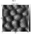
- a diagram representing the surface morphology in 2 ⁇ 2 ⁇ m 2 observed under an atomic force microscope is illustrated in Fig. 3 .
- the state of the surface (main surface) observed under an atomic force microscope was evaluated according to the three ranks in the same manner as in Example 1.
- a diagram representing the surface morphology in 2 ⁇ 2 ⁇ m 2 observed under an atomic force microscope is illustrated in Fig. 4 .
- the state of the surface (main surface) observed under an atomic force microscope was evaluated according to the three ranks in the same manner as in Example 1.
- the group III nitride semiconductor is manufactured by the method of the invention, it is the most effective for the characteristics of a light emitting device that the smoothness of the respective layers forming the active layer is improved and the steepness of the interface is improved. Accordingly, in Example 4 and Comparative Example 3 as described below, manufacturing examples of the group III nitride semiconductor in which an active layer is grown on a laminate obtained by growing a group III nitride single crystal layer on a base substrate are described.
- Three barrier layers and three well layers were alternately grown under the same conditions as those described above, and then a barrier layer was grown by 20 nm under the same conditions as those described above.
- the RMS in 2 ⁇ 2 ⁇ m 2 of the barrier layer after being grown measured by using an atomic force microscope was 0.11 nm.
- a diagram representing the surface morphology in 2 ⁇ 2 ⁇ m 2 observed under an atomic force microscope is illustrated in Fig. 5 .
- the RMS in 2 ⁇ 2 ⁇ m 2 of the barrier layer after being grown measured by using an atomic force microscope was 0.27 nm.
- a diagram representing the surface morphology in 2 ⁇ 2 ⁇ m 2 observed under an atomic force microscope is illustrated in Fig. 6 .
Landscapes
- Chemical & Material Sciences (AREA)
- Metallurgy (AREA)
- Engineering & Computer Science (AREA)
- Materials Engineering (AREA)
- Organic Chemistry (AREA)
- Crystallography & Structural Chemistry (AREA)
- General Chemical & Material Sciences (AREA)
- Chemical Kinetics & Catalysis (AREA)
- Inorganic Chemistry (AREA)
- Mechanical Engineering (AREA)
- Led Devices (AREA)
- Crystals, And After-Treatments Of Crystals (AREA)
- Chemical Vapour Deposition (AREA)
Claims (3)
- Verfahren zum Herstellen eines Gruppe-III-Nitridlaminats (13) durch ein MOCVD-Verfahren mit Zuführen eines Gruppe-III-Rohmaterialgases und eines Stickstoffquellegases auf eine Hauptoberfläche (11a) eines Aluminiumnitrideinkristallsubstrats (11) und Züchten einer Schicht (12), die einen Gruppe-III-Nitrideinkristall enthält, der durch AlXInYGaZN dargestellt ist, wobei X, Y und Z in der Zusammensetzungsformel die Beziehung X + Y + Z = 1,0, 0,85 ≤ X < 0,99, 0,00 ≤ Y < 0,14 und 0,01 < Z ≤ 0,15 erfüllen, auf der Hauptoberfläche (11a) des Aluminiumnitrideinkristallsubstrats (11),wobei eine Oberfläche der Schicht (12), die den Gruppe-III-Nitrideinkristall enthält, einen quadratischen Mittelwert der Rauheit (RMS) in einem Bereich von 2 × 2 µm2 von 0,5 nm oder weniger aufweist, gemessen unter Verwendung eines Rasterkraftmikroskops, und wobeidas Gruppe-III-Rohmaterialgas mindestens ein Gas ist, das aus der Gruppe ausgewählt ist, die aus Trimethylaluminium, Trimethylgallium und Trimethylindium besteht, und das Stickstoffquellegas Ammoniak ist,eine Züchtungstemperatur beim Züchten der Schicht (12), die den Gruppe-III-Nitrideinkristall enthält, auf 1000 °C oder mehr und 1200 °C oder weniger eingestellt wird,eine Züchtungsrate beim Züchten der Schicht (12), die den Gruppe-III-Nitrideinkristall enthält, auf 0,1 µm/h oder mehr und 0,5 µm/h oder weniger eingestellt wird, undein V/III-Verhältnis, das ein Molverhältnis des Stickstoffquellegases zu dem Gruppe-III-Rohmaterialgas darstellt, auf 5000 oder mehr und 15000 oder weniger eingestellt wird.
- Verfahren zum Herstellen eines Gruppe-III-Nitridlaminats (13) nach Anspruch 1, wobei die Schicht (12), die den Gruppe-III-Nitrideinkristall enthält, ein Dotiermittel enthält.
- Verfahren zum Fertigen eines Gruppe-III-Nitridhalbleiters (17), das das Herstellen eines Gruppe-III-Nitridlaminats (13) durch das Verfahren nach Anspruch 1 oder 2 und dann das Bilden mindestens einer aktiven Schicht (15) und einer p-Typ-Schicht (16) auf der Gruppe-III-Nitrideinkristallschicht (12) umfasst.
Applications Claiming Priority (2)
| Application Number | Priority Date | Filing Date | Title |
|---|---|---|---|
| JP2016060197 | 2016-03-24 | ||
| PCT/JP2017/010408 WO2017164036A1 (ja) | 2016-03-24 | 2017-03-15 | Iii族窒化物積層体の製造方法 |
Publications (3)
| Publication Number | Publication Date |
|---|---|
| EP3435407A1 EP3435407A1 (de) | 2019-01-30 |
| EP3435407A4 EP3435407A4 (de) | 2019-11-06 |
| EP3435407B1 true EP3435407B1 (de) | 2024-11-20 |
Family
ID=59900273
Family Applications (1)
| Application Number | Title | Priority Date | Filing Date |
|---|---|---|---|
| EP17770079.6A Active EP3435407B1 (de) | 2016-03-24 | 2017-03-15 | Verfahren zur herstellung eines gruppe-iii-nitrid-laminats |
Country Status (4)
| Country | Link |
|---|---|
| US (1) | US20190103273A1 (de) |
| EP (1) | EP3435407B1 (de) |
| JP (1) | JPWO2017164036A1 (de) |
| WO (1) | WO2017164036A1 (de) |
Families Citing this family (2)
| Publication number | Priority date | Publication date | Assignee | Title |
|---|---|---|---|---|
| JPWO2020017207A1 (ja) * | 2018-07-20 | 2021-08-02 | ソニーセミコンダクタソリューションズ株式会社 | 半導体発光素子 |
| JP2021027297A (ja) * | 2019-08-08 | 2021-02-22 | 住友化学株式会社 | エピタキシャル基板およびその製造方法 |
Family Cites Families (13)
| Publication number | Priority date | Publication date | Assignee | Title |
|---|---|---|---|---|
| JP3866540B2 (ja) * | 2001-07-06 | 2007-01-10 | 株式会社東芝 | 窒化物半導体素子およびその製造方法 |
| US6900474B2 (en) * | 2002-12-20 | 2005-05-31 | Lumileds Lighting U.S., Llc | Light emitting devices with compact active regions |
| JP4316454B2 (ja) * | 2004-09-10 | 2009-08-19 | 株式会社東芝 | 半導体基板、半導体素子、半導体素子の製造方法及び半導体基板の製造方法 |
| JP5401145B2 (ja) * | 2009-03-26 | 2014-01-29 | 株式会社トクヤマ | Iii族窒化物積層体の製造方法 |
| CN102597340B (zh) * | 2009-11-10 | 2015-04-08 | 株式会社德山 | 叠层体的制造方法 |
| WO2013042297A1 (ja) * | 2011-09-20 | 2013-03-28 | パナソニック株式会社 | 窒化ガリウム系化合物半導体発光素子及びそれを用いた光源装置 |
| JP5319810B2 (ja) * | 2012-03-08 | 2013-10-16 | 株式会社東芝 | 窒化物半導体層の製造方法 |
| JP6151487B2 (ja) * | 2012-07-10 | 2017-06-21 | 富士通株式会社 | 化合物半導体装置及びその製造方法 |
| JP6088807B2 (ja) * | 2012-11-19 | 2017-03-01 | スタンレー電気株式会社 | 半導体発光素子及びその製造方法 |
| JP6168978B2 (ja) * | 2013-12-09 | 2017-07-26 | 古河電気工業株式会社 | 窒化物半導体装置およびその製造方法、ならびにダイオードおよび電界効果トランジスタ |
| JP6356530B2 (ja) * | 2014-08-08 | 2018-07-11 | ウシオ電機株式会社 | 窒化物半導体発光素子及びその製造方法 |
| KR102212561B1 (ko) * | 2014-08-11 | 2021-02-08 | 삼성전자주식회사 | 반도체 발광 소자 및 반도체 발광 소자 패키지 |
| US10224458B2 (en) * | 2015-03-06 | 2019-03-05 | Stanley Electric Co., Ltd. | Group III nitride laminate, luminescence element comprising said laminate, and method of producing group III nitride laminate |
-
2017
- 2017-03-15 WO PCT/JP2017/010408 patent/WO2017164036A1/ja not_active Ceased
- 2017-03-15 EP EP17770079.6A patent/EP3435407B1/de active Active
- 2017-03-15 JP JP2018507261A patent/JPWO2017164036A1/ja active Pending
- 2017-03-15 US US16/087,360 patent/US20190103273A1/en not_active Abandoned
Also Published As
| Publication number | Publication date |
|---|---|
| JPWO2017164036A1 (ja) | 2019-01-31 |
| EP3435407A1 (de) | 2019-01-30 |
| US20190103273A1 (en) | 2019-04-04 |
| EP3435407A4 (de) | 2019-11-06 |
| WO2017164036A1 (ja) | 2017-09-28 |
Similar Documents
| Publication | Publication Date | Title |
|---|---|---|
| JP4964672B2 (ja) | 低抵抗率炭化珪素単結晶基板 | |
| EP2896725B1 (de) | Aluminiumnitridsubstrat und gruppe-iii-nitridlaminat | |
| JP5319810B2 (ja) | 窒化物半導体層の製造方法 | |
| CN101996862B (zh) | 氮化物半导体自支撑衬底、氮化物半导体自支撑衬底的制造方法以及氮化物半导体装置 | |
| EP2484816B1 (de) | Verfahren zur herstellung eines laminats | |
| US9431489B2 (en) | β-Ga2O3-based single crystal substrate | |
| EP3514265B1 (de) | Lichtemittierendes halbleiterbauelement zur emission ultravioletten lichts | |
| WO2012144614A1 (ja) | エピタキシャル炭化珪素単結晶基板及びその製造方法 | |
| US9896780B2 (en) | Method for pretreatment of base substrate and method for manufacturing layered body using pretreated base substrate | |
| JP2004111848A (ja) | サファイア基板とそれを用いたエピタキシャル基板およびその製造方法 | |
| JP5931737B2 (ja) | 光学素子の製造方法 | |
| EP3435407B1 (de) | Verfahren zur herstellung eines gruppe-iii-nitrid-laminats | |
| JP4359770B2 (ja) | Iii−v族窒化物系半導体基板及びその製造ロット | |
| US8466471B2 (en) | Nitride semiconductor free-standing substrate and method for making same | |
| JP7800516B2 (ja) | 積層体 | |
| KR100841269B1 (ko) | Ⅲ족 질화물 반도체 다층구조물 | |
| JP7704399B2 (ja) | Ga2O3系単結晶基板並びにAlxGa(1-x)N系半導体積層体の製造方法 | |
| JP2016082200A (ja) | 結晶積層構造体及びその製造方法、並びに半導体素子 | |
| JP4216580B2 (ja) | ZnTe系化合物半導体の表面処理方法および半導体装置の製造方法 | |
| JP4733729B2 (ja) | ZnTe系化合物半導体の表面処理方法および半導体装置の製造方法 | |
| JP4420128B2 (ja) | Iii−v族窒化物系半導体デバイス及びその製造方法 | |
| CN118610071A (zh) | 复合结构氮化铝单晶复合衬底及其制备方法、紫外发光器件 | |
| JP2010199598A (ja) | Iii−v族窒化物系半導体基板 | |
| JP2016072399A (ja) | 窒化物半導体テンプレートの製造方法 |
Legal Events
| Date | Code | Title | Description |
|---|---|---|---|
| STAA | Information on the status of an ep patent application or granted ep patent |
Free format text: STATUS: THE INTERNATIONAL PUBLICATION HAS BEEN MADE |
|
| PUAI | Public reference made under article 153(3) epc to a published international application that has entered the european phase |
Free format text: ORIGINAL CODE: 0009012 |
|
| STAA | Information on the status of an ep patent application or granted ep patent |
Free format text: STATUS: REQUEST FOR EXAMINATION WAS MADE |
|
| 17P | Request for examination filed |
Effective date: 20180921 |
|
| AK | Designated contracting states |
Kind code of ref document: A1 Designated state(s): AL AT BE BG CH CY CZ DE DK EE ES FI FR GB GR HR HU IE IS IT LI LT LU LV MC MK MT NL NO PL PT RO RS SE SI SK SM TR |
|
| AX | Request for extension of the european patent |
Extension state: BA ME |
|
| DAV | Request for validation of the european patent (deleted) | ||
| DAX | Request for extension of the european patent (deleted) | ||
| A4 | Supplementary search report drawn up and despatched |
Effective date: 20191009 |
|
| RIC1 | Information provided on ipc code assigned before grant |
Ipc: C30B 29/38 20060101ALI20191002BHEP Ipc: H01L 21/02 20060101ALI20191002BHEP Ipc: C30B 25/16 20060101ALI20191002BHEP Ipc: C23C 16/34 20060101ALI20191002BHEP Ipc: H01L 21/205 20060101AFI20191002BHEP Ipc: C30B 25/18 20060101ALI20191002BHEP Ipc: C30B 29/40 20060101ALI20191002BHEP Ipc: C30B 25/14 20060101ALI20191002BHEP |
|
| STAA | Information on the status of an ep patent application or granted ep patent |
Free format text: STATUS: EXAMINATION IS IN PROGRESS |
|
| 17Q | First examination report despatched |
Effective date: 20210928 |
|
| GRAP | Despatch of communication of intention to grant a patent |
Free format text: ORIGINAL CODE: EPIDOSNIGR1 |
|
| STAA | Information on the status of an ep patent application or granted ep patent |
Free format text: STATUS: GRANT OF PATENT IS INTENDED |
|
| INTG | Intention to grant announced |
Effective date: 20240319 |
|
| RIN1 | Information on inventor provided before grant (corrected) |
Inventor name: FURUYA, HIROSHI |
|
| GRAJ | Information related to disapproval of communication of intention to grant by the applicant or resumption of examination proceedings by the epo deleted |
Free format text: ORIGINAL CODE: EPIDOSDIGR1 |
|
| STAA | Information on the status of an ep patent application or granted ep patent |
Free format text: STATUS: EXAMINATION IS IN PROGRESS |
|
| GRAP | Despatch of communication of intention to grant a patent |
Free format text: ORIGINAL CODE: EPIDOSNIGR1 |
|
| GRAP | Despatch of communication of intention to grant a patent |
Free format text: ORIGINAL CODE: EPIDOSNIGR1 |
|
| STAA | Information on the status of an ep patent application or granted ep patent |
Free format text: STATUS: GRANT OF PATENT IS INTENDED |
|
| INTC | Intention to grant announced (deleted) | ||
| INTG | Intention to grant announced |
Effective date: 20240614 |
|
| GRAS | Grant fee paid |
Free format text: ORIGINAL CODE: EPIDOSNIGR3 |
|
| GRAA | (expected) grant |
Free format text: ORIGINAL CODE: 0009210 |
|
| STAA | Information on the status of an ep patent application or granted ep patent |
Free format text: STATUS: THE PATENT HAS BEEN GRANTED |
|
| AK | Designated contracting states |
Kind code of ref document: B1 Designated state(s): AL AT BE BG CH CY CZ DE DK EE ES FI FR GB GR HR HU IE IS IT LI LT LU LV MC MK MT NL NO PL PT RO RS SE SI SK SM TR |
|
| REG | Reference to a national code |
Ref country code: GB Ref legal event code: FG4D |
|
| REG | Reference to a national code |
Ref country code: CH Ref legal event code: EP |
|
| REG | Reference to a national code |
Ref country code: DE Ref legal event code: R096 Ref document number: 602017086251 Country of ref document: DE |
|
| REG | Reference to a national code |
Ref country code: IE Ref legal event code: FG4D |
|
| REG | Reference to a national code |
Ref country code: LT Ref legal event code: MG9D |
|
| REG | Reference to a national code |
Ref country code: NL Ref legal event code: MP Effective date: 20241120 |
|
| PG25 | Lapsed in a contracting state [announced via postgrant information from national office to epo] |
Ref country code: PT Free format text: LAPSE BECAUSE OF FAILURE TO SUBMIT A TRANSLATION OF THE DESCRIPTION OR TO PAY THE FEE WITHIN THE PRESCRIBED TIME-LIMIT Effective date: 20250320 Ref country code: HR Free format text: LAPSE BECAUSE OF FAILURE TO SUBMIT A TRANSLATION OF THE DESCRIPTION OR TO PAY THE FEE WITHIN THE PRESCRIBED TIME-LIMIT Effective date: 20241120 Ref country code: IS Free format text: LAPSE BECAUSE OF FAILURE TO SUBMIT A TRANSLATION OF THE DESCRIPTION OR TO PAY THE FEE WITHIN THE PRESCRIBED TIME-LIMIT Effective date: 20250320 |
|
| PG25 | Lapsed in a contracting state [announced via postgrant information from national office to epo] |
Ref country code: FI Free format text: LAPSE BECAUSE OF FAILURE TO SUBMIT A TRANSLATION OF THE DESCRIPTION OR TO PAY THE FEE WITHIN THE PRESCRIBED TIME-LIMIT Effective date: 20241120 Ref country code: NL Free format text: LAPSE BECAUSE OF FAILURE TO SUBMIT A TRANSLATION OF THE DESCRIPTION OR TO PAY THE FEE WITHIN THE PRESCRIBED TIME-LIMIT Effective date: 20241120 |
|
| REG | Reference to a national code |
Ref country code: AT Ref legal event code: MK05 Ref document number: 1744385 Country of ref document: AT Kind code of ref document: T Effective date: 20241120 |
|
| PG25 | Lapsed in a contracting state [announced via postgrant information from national office to epo] |
Ref country code: BG Free format text: LAPSE BECAUSE OF FAILURE TO SUBMIT A TRANSLATION OF THE DESCRIPTION OR TO PAY THE FEE WITHIN THE PRESCRIBED TIME-LIMIT Effective date: 20241120 |
|
| PG25 | Lapsed in a contracting state [announced via postgrant information from national office to epo] |
Ref country code: ES Free format text: LAPSE BECAUSE OF FAILURE TO SUBMIT A TRANSLATION OF THE DESCRIPTION OR TO PAY THE FEE WITHIN THE PRESCRIBED TIME-LIMIT Effective date: 20241120 |
|
| PG25 | Lapsed in a contracting state [announced via postgrant information from national office to epo] |
Ref country code: NO Free format text: LAPSE BECAUSE OF FAILURE TO SUBMIT A TRANSLATION OF THE DESCRIPTION OR TO PAY THE FEE WITHIN THE PRESCRIBED TIME-LIMIT Effective date: 20250220 |
|
| PG25 | Lapsed in a contracting state [announced via postgrant information from national office to epo] |
Ref country code: LV Free format text: LAPSE BECAUSE OF FAILURE TO SUBMIT A TRANSLATION OF THE DESCRIPTION OR TO PAY THE FEE WITHIN THE PRESCRIBED TIME-LIMIT Effective date: 20241120 Ref country code: AT Free format text: LAPSE BECAUSE OF FAILURE TO SUBMIT A TRANSLATION OF THE DESCRIPTION OR TO PAY THE FEE WITHIN THE PRESCRIBED TIME-LIMIT Effective date: 20241120 Ref country code: GR Free format text: LAPSE BECAUSE OF FAILURE TO SUBMIT A TRANSLATION OF THE DESCRIPTION OR TO PAY THE FEE WITHIN THE PRESCRIBED TIME-LIMIT Effective date: 20250221 |
|
| PG25 | Lapsed in a contracting state [announced via postgrant information from national office to epo] |
Ref country code: PL Free format text: LAPSE BECAUSE OF FAILURE TO SUBMIT A TRANSLATION OF THE DESCRIPTION OR TO PAY THE FEE WITHIN THE PRESCRIBED TIME-LIMIT Effective date: 20241120 |
|
| PG25 | Lapsed in a contracting state [announced via postgrant information from national office to epo] |
Ref country code: RS Free format text: LAPSE BECAUSE OF FAILURE TO SUBMIT A TRANSLATION OF THE DESCRIPTION OR TO PAY THE FEE WITHIN THE PRESCRIBED TIME-LIMIT Effective date: 20250220 |
|
| PG25 | Lapsed in a contracting state [announced via postgrant information from national office to epo] |
Ref country code: SM Free format text: LAPSE BECAUSE OF FAILURE TO SUBMIT A TRANSLATION OF THE DESCRIPTION OR TO PAY THE FEE WITHIN THE PRESCRIBED TIME-LIMIT Effective date: 20241120 |
|
| PG25 | Lapsed in a contracting state [announced via postgrant information from national office to epo] |
Ref country code: DK Free format text: LAPSE BECAUSE OF FAILURE TO SUBMIT A TRANSLATION OF THE DESCRIPTION OR TO PAY THE FEE WITHIN THE PRESCRIBED TIME-LIMIT Effective date: 20241120 |
|
| PG25 | Lapsed in a contracting state [announced via postgrant information from national office to epo] |
Ref country code: EE Free format text: LAPSE BECAUSE OF FAILURE TO SUBMIT A TRANSLATION OF THE DESCRIPTION OR TO PAY THE FEE WITHIN THE PRESCRIBED TIME-LIMIT Effective date: 20241120 |
|
| PG25 | Lapsed in a contracting state [announced via postgrant information from national office to epo] |
Ref country code: RO Free format text: LAPSE BECAUSE OF FAILURE TO SUBMIT A TRANSLATION OF THE DESCRIPTION OR TO PAY THE FEE WITHIN THE PRESCRIBED TIME-LIMIT Effective date: 20241120 |
|
| PG25 | Lapsed in a contracting state [announced via postgrant information from national office to epo] |
Ref country code: SK Free format text: LAPSE BECAUSE OF FAILURE TO SUBMIT A TRANSLATION OF THE DESCRIPTION OR TO PAY THE FEE WITHIN THE PRESCRIBED TIME-LIMIT Effective date: 20241120 |
|
| PG25 | Lapsed in a contracting state [announced via postgrant information from national office to epo] |
Ref country code: CZ Free format text: LAPSE BECAUSE OF FAILURE TO SUBMIT A TRANSLATION OF THE DESCRIPTION OR TO PAY THE FEE WITHIN THE PRESCRIBED TIME-LIMIT Effective date: 20241120 |
|
| PG25 | Lapsed in a contracting state [announced via postgrant information from national office to epo] |
Ref country code: IT Free format text: LAPSE BECAUSE OF FAILURE TO SUBMIT A TRANSLATION OF THE DESCRIPTION OR TO PAY THE FEE WITHIN THE PRESCRIBED TIME-LIMIT Effective date: 20241120 |
|
| REG | Reference to a national code |
Ref country code: DE Ref legal event code: R097 Ref document number: 602017086251 Country of ref document: DE |
|
| PG25 | Lapsed in a contracting state [announced via postgrant information from national office to epo] |
Ref country code: SE Free format text: LAPSE BECAUSE OF FAILURE TO SUBMIT A TRANSLATION OF THE DESCRIPTION OR TO PAY THE FEE WITHIN THE PRESCRIBED TIME-LIMIT Effective date: 20241120 |
|
| PLBE | No opposition filed within time limit |
Free format text: ORIGINAL CODE: 0009261 |
|
| STAA | Information on the status of an ep patent application or granted ep patent |
Free format text: STATUS: NO OPPOSITION FILED WITHIN TIME LIMIT |
|
| PG25 | Lapsed in a contracting state [announced via postgrant information from national office to epo] |
Ref country code: MC Free format text: LAPSE BECAUSE OF FAILURE TO SUBMIT A TRANSLATION OF THE DESCRIPTION OR TO PAY THE FEE WITHIN THE PRESCRIBED TIME-LIMIT Effective date: 20241120 |
|
| 26N | No opposition filed |
Effective date: 20250821 |
|
| REG | Reference to a national code |
Ref country code: CH Ref legal event code: H13 Free format text: ST27 STATUS EVENT CODE: U-0-0-H10-H13 (AS PROVIDED BY THE NATIONAL OFFICE) Effective date: 20251023 |
|
| PG25 | Lapsed in a contracting state [announced via postgrant information from national office to epo] |
Ref country code: LU Free format text: LAPSE BECAUSE OF NON-PAYMENT OF DUE FEES Effective date: 20250315 |
|
| REG | Reference to a national code |
Ref country code: DE Ref legal event code: R079 Ref document number: 602017086251 Country of ref document: DE Free format text: PREVIOUS MAIN CLASS: H01L0021205000 Ipc: H10P0014240000 |
|
| REG | Reference to a national code |
Ref country code: BE Ref legal event code: MM Effective date: 20250331 |
|
| PG25 | Lapsed in a contracting state [announced via postgrant information from national office to epo] |
Ref country code: BE Free format text: LAPSE BECAUSE OF NON-PAYMENT OF DUE FEES Effective date: 20250331 |
|
| PG25 | Lapsed in a contracting state [announced via postgrant information from national office to epo] |
Ref country code: CH Free format text: LAPSE BECAUSE OF NON-PAYMENT OF DUE FEES Effective date: 20250331 |
|
| PG25 | Lapsed in a contracting state [announced via postgrant information from national office to epo] |
Ref country code: IE Free format text: LAPSE BECAUSE OF NON-PAYMENT OF DUE FEES Effective date: 20250315 |
|
| PGFP | Annual fee paid to national office [announced via postgrant information from national office to epo] |
Ref country code: GB Payment date: 20260202 Year of fee payment: 10 |
|
| PGFP | Annual fee paid to national office [announced via postgrant information from national office to epo] |
Ref country code: DE Payment date: 20260128 Year of fee payment: 10 |
|
| PGFP | Annual fee paid to national office [announced via postgrant information from national office to epo] |
Ref country code: FR Payment date: 20260209 Year of fee payment: 10 |