EP3433924B1 - Reglersteuerschaltung - Google Patents
Reglersteuerschaltung Download PDFInfo
- Publication number
- EP3433924B1 EP3433924B1 EP17713062.2A EP17713062A EP3433924B1 EP 3433924 B1 EP3433924 B1 EP 3433924B1 EP 17713062 A EP17713062 A EP 17713062A EP 3433924 B1 EP3433924 B1 EP 3433924B1
- Authority
- EP
- European Patent Office
- Prior art keywords
- voltage
- output
- regulator
- switching regulator
- sensor
- Prior art date
- Legal status (The legal status is an assumption and is not a legal conclusion. Google has not performed a legal analysis and makes no representation as to the accuracy of the status listed.)
- Active
Links
Images

Classifications
-
- H—ELECTRICITY
- H02—GENERATION; CONVERSION OR DISTRIBUTION OF ELECTRIC POWER
- H02M—APPARATUS FOR CONVERSION BETWEEN AC AND AC, BETWEEN AC AND DC, OR BETWEEN DC AND DC, AND FOR USE WITH MAINS OR SIMILAR POWER SUPPLY SYSTEMS; CONVERSION OF DC OR AC INPUT POWER INTO SURGE OUTPUT POWER; CONTROL OR REGULATION THEREOF
- H02M3/00—Conversion of DC power input into DC power output
- H02M3/02—Conversion of DC power input into DC power output without intermediate conversion into AC
- H02M3/04—Conversion of DC power input into DC power output without intermediate conversion into AC by static converters
- H02M3/10—Conversion of DC power input into DC power output without intermediate conversion into AC by static converters using discharge tubes with control electrode or semiconductor devices with control electrode
- H02M3/145—Conversion of DC power input into DC power output without intermediate conversion into AC by static converters using discharge tubes with control electrode or semiconductor devices with control electrode using devices of a triode or transistor type requiring continuous application of a control signal
- H02M3/155—Conversion of DC power input into DC power output without intermediate conversion into AC by static converters using discharge tubes with control electrode or semiconductor devices with control electrode using devices of a triode or transistor type requiring continuous application of a control signal using semiconductor devices only
- H02M3/156—Conversion of DC power input into DC power output without intermediate conversion into AC by static converters using discharge tubes with control electrode or semiconductor devices with control electrode using devices of a triode or transistor type requiring continuous application of a control signal using semiconductor devices only with automatic control of output voltage or current, e.g. switching regulators
-
- H—ELECTRICITY
- H02—GENERATION; CONVERSION OR DISTRIBUTION OF ELECTRIC POWER
- H02J—ELECTRIC POWER NETWORKS; CIRCUIT ARRANGEMENTS OR SYSTEMS FOR SUPPLYING OR DISTRIBUTING ELECTRIC POWER; SYSTEMS FOR STORING ELECTRIC ENERGY
- H02J7/00—Circuit arrangements for charging or discharging batteries or for supplying loads from batteries
- H02J7/90—Regulation of charging or discharging current or voltage
- H02J7/96—Regulation of charging or discharging current or voltage in response to battery voltage
- H02J7/963—Regulation of charging or discharging current or voltage in response to battery voltage in response to battery voltage gradient
-
- G—PHYSICS
- G05—CONTROLLING; REGULATING
- G05F—SYSTEMS FOR REGULATING ELECTRIC OR MAGNETIC VARIABLES
- G05F1/00—Automatic systems in which deviations of an electric quantity from one or more predetermined values are detected at the output of the system and fed back to a device within the system to restore the detected quantity to its predetermined value or values, i.e. retroactive systems
- G05F1/10—Regulating voltage or current
- G05F1/46—Regulating voltage or current wherein the variable actually regulated by the final control device is DC
- G05F1/56—Regulating voltage or current wherein the variable actually regulated by the final control device is DC using semiconductor devices in series with the load as final control devices
- G05F1/565—Regulating voltage or current wherein the variable actually regulated by the final control device is DC using semiconductor devices in series with the load as final control devices sensing a condition of the system or its load in addition to means responsive to deviations in the output of the system, e.g. current, voltage, power factor
-
- H—ELECTRICITY
- H02—GENERATION; CONVERSION OR DISTRIBUTION OF ELECTRIC POWER
- H02J—ELECTRIC POWER NETWORKS; CIRCUIT ARRANGEMENTS OR SYSTEMS FOR SUPPLYING OR DISTRIBUTING ELECTRIC POWER; SYSTEMS FOR STORING ELECTRIC ENERGY
- H02J7/00—Circuit arrangements for charging or discharging batteries or for supplying loads from batteries
- H02J7/90—Regulation of charging or discharging current or voltage
- H02J7/94—Regulation of charging or discharging current or voltage in response to battery current
- H02J7/953—Regulation of charging or discharging current or voltage in response to battery current in response to charge current gradient
-
- H—ELECTRICITY
- H02—GENERATION; CONVERSION OR DISTRIBUTION OF ELECTRIC POWER
- H02M—APPARATUS FOR CONVERSION BETWEEN AC AND AC, BETWEEN AC AND DC, OR BETWEEN DC AND DC, AND FOR USE WITH MAINS OR SIMILAR POWER SUPPLY SYSTEMS; CONVERSION OF DC OR AC INPUT POWER INTO SURGE OUTPUT POWER; CONTROL OR REGULATION THEREOF
- H02M3/00—Conversion of DC power input into DC power output
- H02M3/22—Conversion of DC power input into DC power output with intermediate conversion into AC
- H02M3/24—Conversion of DC power input into DC power output with intermediate conversion into AC by static converters
- H02M3/28—Conversion of DC power input into DC power output with intermediate conversion into AC by static converters using discharge tubes with control electrode or semiconductor devices with control electrode to produce the intermediate AC
- H02M3/325—Conversion of DC power input into DC power output with intermediate conversion into AC by static converters using discharge tubes with control electrode or semiconductor devices with control electrode to produce the intermediate AC using devices of a triode or a transistor type requiring continuous application of a control signal
- H02M3/335—Conversion of DC power input into DC power output with intermediate conversion into AC by static converters using discharge tubes with control electrode or semiconductor devices with control electrode to produce the intermediate AC using devices of a triode or a transistor type requiring continuous application of a control signal using semiconductor devices only
- H02M3/33507—Conversion of DC power input into DC power output with intermediate conversion into AC by static converters using discharge tubes with control electrode or semiconductor devices with control electrode to produce the intermediate AC using devices of a triode or a transistor type requiring continuous application of a control signal using semiconductor devices only with automatic control of the output voltage or current, e.g. flyback converters
-
- H—ELECTRICITY
- H02—GENERATION; CONVERSION OR DISTRIBUTION OF ELECTRIC POWER
- H02M—APPARATUS FOR CONVERSION BETWEEN AC AND AC, BETWEEN AC AND DC, OR BETWEEN DC AND DC, AND FOR USE WITH MAINS OR SIMILAR POWER SUPPLY SYSTEMS; CONVERSION OF DC OR AC INPUT POWER INTO SURGE OUTPUT POWER; CONTROL OR REGULATION THEREOF
- H02M1/00—Details of apparatus for conversion
- H02M1/0003—Details of control, feedback or regulation circuits
Definitions
- Embodiments of the present invention relate to electrical supply control circuits for regulating a supply voltage to track a reference voltage.
- some embodiments relate to electrical supply control circuits for using in powering analogue circuits which may form part of a braking system of a vehicle.
- ADC analogue-to-digital converter
- US2013154579 discloses a capacitor device includes a capacitor unit, a voltage-dividing circuit for outputting a divided voltage obtained by dividing a voltage of the capacitor unit, and a comparator circuit.
- the comparator circuit causes the charge circuit to operate such that the voltage of the capacitor unit reaches a full-charge voltage.
- the voltage-dividing circuit includes a semiconductor switching element, and outputs a divided voltage.
- a control circuit is operable to determine the full-charge voltage to be a high-temperature full-charge voltage by turning off the first semiconductor switching element when a temperature at the capacitor unit exceeds a reference temperature.
- the control circuit is operable to determine the full-charge voltage to be a low-temperature full-charge voltage that is higher than the high-temperature full-charge voltage by turning on the first semiconductor switching element when the detected temperature is not higher than the reference temperature.
- an aspect of the present invention provides a sensor circuit including a regulator control circuit, a switching regulator, and at least one analogue sensor connected to an output of the switching regulator, wherein the regulator control circuit is configured to control the switching regulator and includes: a feedback comparator configured to compare a signal representative of a reference voltage with a signal representative of a voltage output of the switching regulator and to output a control signal for controlling the operation of the switching regulator dependent on the signals received by the feedback comparator; and a current feedback controller connected to the feedback comparator and configured to receive a signal representative of a current output by the switching regulator and determine whether the regulator control circuit adopts a first or second mode of operation based on the signal representative of a current output, such that, in the first mode of operation, the control signal is for controlling the switching regulator in accordance with a constant voltage control scheme, in the second mode of operation, the control signal is for controlling the switching regulator in accordance with a constant current control scheme, and the sensor is provided with power at a voltage which tracks the reference voltage and wherein the analogue sensor
- the second mode may be adopted when the signal representative of the current output by the switching regulator exceeds a predetermined current.
- the current feedback controller may be configured to modify the signal representative of the voltage output of the switching regulator in order to cause the adoption of the second mode.
- the regulator control circuit may further include a first drive switch circuit which is configured to receive an output from the current feedback controller and selectively to control an input of the current feedback controller dependent on the output from the current feedback controller.
- the regulator control circuit may further include a regulator drive circuit which is configured to receive the output from the feedback comparator and to control the operation of the switching regulator in accordance with the output from the feedback comparator.
- the regulator control circuit may be further configured to clamp the output of the switching regulator to a clamp voltage and to modify the control signal to disable the switching regulator when the signal representative of the voltage output of the switching regulator and the signal representative of the reference voltage indicate that the voltage output is higher than the reference voltage.
- the regulator control circuit may further include an output voltage transient protection circuit configured to protect the feedback comparator from high voltage transients in the output voltage.
- the current feedback controller may be further configured to determine whether the regulator control circuit adopts a fourth mode of operation in which hybrid pulse width and pulse frequency modulation is used to control the operation of the switching regulator.
- Another aspect may provide a braking system for a vehicle including a sensor circuit as above.
- Another aspect provides a vehicle including a braking system as above or a sensor circuit as above.
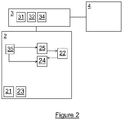
- the present invention includes a vehicle 1 to which a braking system 2 has been fitted.
- vehicle 1 may include a truck 11 and trailer 12, the trailer 12 being configured to be towed by the truck 11.
- the braking system 2 may, therefore, include a portion which is part of the truck 11 and a portion which is part of the trailer 12.
- Other configurations of braking system 2 and vehicle 1 may, however, be used in other embodiments.
- the braking system 2 includes a brake module 21 which is configured, on actuation, to apply a braking force to one or more ground engaging wheels of the vehicle 1 (e.g. of the truck 11 and/or trailer 12) in order to slow the vehicle 1 and/or substantially prevent its movement.
- the braking system 2 may also include one or more analogue sensors 22.
- the or each analogue sensor 22 may be configured to measure a parameter associated with the operation of the vehicle 1 (which may include a parameter associated with the operation of the truck 11, and/or of the trailer 12, and/or of the braking system 2 (which may include the braking module 21)). Examples of such analogue sensors 22 may include pressure sensors, position sensors, temperature sensors, and acceleration sensors. In some embodiments, the or each analogue sensor 22 may include a sensor which measures the speed of the vehicle 1 (which may be the speed of the truck 11 or trailer 12) and/or may be configured to measure the speed of rotation of one or more ground engaging wheels of the vehicle 1 (which may include a ground engaging wheel of the truck 11 and/or the trailer 12). The or each analogue sensor 22 may include a potentiometric sensor device.
- the or each analogue sensor 22 may be used by other parts of the braking system 2 to determine one or more parameters regarding the operation of the vehicle 1 or braking system 2, so that another aspect of the braking system 2 can be controlled based, at least in part, on the one or more parameters.
- the braking system 2 may include a braking system controller 23 which is configured to receive the one or more parameters from the one or more analogue sensors 22 and to output a control signal to part of the braking system 2 (e.g. to the braking module 21), the control signal being at least partly based on the one or more received parameters.
- a braking system controller 23 which is configured to receive the one or more parameters from the one or more analogue sensors 22 and to output a control signal to part of the braking system 2 (e.g. to the braking module 21), the control signal being at least partly based on the one or more received parameters.
- the braking system 2 may include an analogue-to-digital converter (ADC) 24 which is configured to receive an analogue signal representative of a parameter from an analogue sensor 22 of the one or more analogue sensors 22.
- the ADC 24 may be configured to convert the received analogue signal into a digital signal which is then provided, by the ADC 24, to the braking system controller 23 - which may be a digital controller (such as a microcontroller or microprocessor device).
- the braking system 2 includes a plurality of ADCs 24, each associated with a different analogue sensor 22.
- a plurality of analogue sensors 22 are associated with the same ADC 24 and the braking system 2 includes a multiplexing device (not shown) which is configured to multiplex the analogue signals output by the plurality of analogue sensors 22 such that the ADC 24 operates on each analogue signal separately in turn.
- the or each analogue sensor 22 may be configured to output an analogue signal in which the parameter being sensed is encoded in changes in the voltage of the analogue signal output by the analogue sensor 22.
- the or each analogue sensor 22 may, therefore, require an electrical supply, e.g. via an electrical supply system 3, which has a predetermined relationship with a reference voltage associated with the ADC 24 - such that the ADC 24 correctly translates the or each received analogue signal into the appropriate digital signal for use by the braking system controller 23.
- analogue sensors 22 are one example of a component which requires an electrical supply which has a predetermined relationship with a reference voltage (e.g. a reference voltage associated with the ADC 24).
- a reference voltage e.g. a reference voltage associated with the ADC 24
- This reference voltage may be provided by a reference voltage output 35 of the electrical supply system 3 of the vehicle 1 or of the braking system 2, for example.
- the reference voltage output 35 may be connected in electrical communication to a reference voltage regulator (not shown) which is configured to reduce or translate the reference voltage output 35 into the reference voltage (which may be a lower voltage than the voltage of the reference voltage output 35).
- the reference voltage regulator is part of the electrical supply system 3 and, in some embodiments, the reference voltage regulator is part of the braking system 2.
- the vehicle 1 includes an electrical supply system 3, see figure 2 , which is configured to provide electrical power to one or more units of the vehicle 1, including the braking system 2 and/or the lighting system 4, if provided.
- an electrical supply system 3 see figure 2 , which is configured to provide electrical power to one or more units of the vehicle 1, including the braking system 2 and/or the lighting system 4, if provided.
- the electrical supply system 3 may include a battery 31 and a generation system 32 (such as an electrical alternator or other generator) which is configured to generate electricity using mechanical power generated by an engine of the vehicle 1, for example.
- the electrical supply system 3 may include an ignition or other power line 34 which is configured, with a ground line, to supply electricity to the one or more units of the vehicle 1.
- the voltage of the electricity supplied through the electrical supply system 3 may be 12V, 24V, or 32V, for example.
- the battery 31 - if provided - may be configured to provide electrical power at any one of these voltages.
- the electrical supply system 3 is also configured to output a reference voltage output 35.
- the reference voltage is at a level suitable for use by logic circuits (such as the ADC 24, and/or the braking system controller 23). In some embodiments, the reference voltage may be about 3V or 5V.
- the reference voltage is subject to variations during operation of the vehicle 1 - which may be due to other demands on the electrical supply system 3 of the vehicle 1 (e.g. during cranking) but could also be the result of faults or the result of connection of an electrical system of the truck 11 with an electrical system of the trailer 12 (or a part of the braking system 2 of the truck 11 with a part of the braking system 2 of the trailer 12).
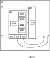
- an electrical supply control system 25 is provided as part of the braking system 3 or otherwise (e.g. as part of the vehicle 1 more generally, which may include being part of the truck 11 and/or trailer 12).
- the electrical supply control system 25 is configured to be coupled in electrical communication with the ignition or other power line 34 and to the electrical power output over the ignition or other power line 34 to a sensor power output for use by the one or more analogue sensors 22.
- the electrical supply control system 25 is configured to convert the voltage of power delivered over the ignition or other power line 34 to a sensor voltage, wherein the sensor voltage substantially tracks the reference voltage - i.e. a substantially constant voltage. In some embodiments, the electrical supply control system 25 is configured to provide the sensor power output at a substantially constant current.
- the electrical supply control system 25, and/or the ADC 24 and/or the reference voltage output 35 may form part of the braking system controller 23.
- some embodiments of the electrical supply control system 25 include a switching regulator 251 and a regulator control circuit 252.
- the switching regulator 251 is configured to receive electrical power from the electrical supply system 3 (e.g. via an ignition or other power line 34) and to convert that electrical power into the sensor power output.
- the operation of the switching regulator 251 is controlled by the regulator control circuit 252 which is configured to provide two or more modes of operation.
- the switching regulator 251 is controlled to provide the sensor power output at the sensor voltage which tracks the reference voltage - i.e. a substantially constant voltage (albeit subject to some variations in practice).
- the switching regulator 251 is controlled to provide the sensor power output at a substantially constant current.
- the switching regulator 251 substantially prevents connection of the sensor power output to the input supply 34 (i.e. the switching regulator 251 may be substantially disabled). This mode of operation may be used, for example, if a fault occurs or is expected (e.g. a short circuit fault as described herein).
- the regulator control circuit 252 may be configured to control the operation of the switching regulator 251 to provide pulse frequency modulated control of the switching regulator 251. In some embodiments, other forms or techniques of control are possible, such as pulse width modulated control. In some embodiments, the regulator control circuit 252 is configured to control the operation of the switching regulator 251 to provide a hybrid pulse width and pulse frequency modulated control of the switching regulator 251 - in such a hybrid, pulse width modulation may be used except when the load on the sensor power output is below a threshold when one or more pulses may be omitted (providing a degree of pulse frequency modulation). This may be viewed, in some embodiments, as a fourth mode of operation.
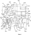
- the switching regulator 251 may, in some embodiments, include a power switch device 2511 which may be a transistor device and may be, for example, a PNP transistor device.
- the switching regulator 251 may further include an energy storage element 2512 such as an inductor.
- the switching regulator 251 may further include a diode 2513.
- the power switch device 2511 is connected in series with the energy storage element 2512.
- the power switch device 2511 is further connected in series with the ignition or other power line 34.
- the ignition or other power line 34 may be connected in selective electrical communication with the energy storage element 2512.
- the power switch device 2511 in an on-state the ignition or other power line 34 may be connected in electrical communication with the energy storage element 2512 such that the energy storage element 2512 is charged.
- the power switch device 2511 in an off-state the ignition or other power line 34 may be disconnected from electrical communication with the energy storage element 2512 which may, as a result, discharge.
- the diode 2513 may be connected in electrical communication with both the power switch device 2511 and the energy storage element 2512 and may remain in electrical communication with the energy storage element 2512 irrespective of the on- or off-state of the power switch device 2511. Accordingly, the diode 2513 may be oriented to allow the charging of the energy storage element 2512 with the power switch device 2511 in the on-state and to allow the discharging of the energy storage element 2512 with the power switch device 2511 in the off-state.
- the energy storage element 2512 may be connected to the sensor voltage line 26 such that the discharging of the energy storage element 2512 is to the sensor voltage line 26.
- a capacitor 2514 of the switching regulator 251 may be connected between the sensor voltage line 26 and a ground connection or line 36.
- the actuation of the power switch device 2511 between the on- and off-states is controlled by the regulator control circuit 252.
- the power switch device 2511 being a transistor device, therefore, the base of the power switch device 2511 is connected in electrical communication with the regulator control circuit 252.
- the power switch device 2511 is a PNP transistor device with its emitter connected in electrical communication with the ignition or other power line 34 and its collector connected in electrical communication with the energy storage element 2512 (and diode 2513, which is also connected in electrical communication with the ground connection or line 36).
- the base of the power switch device 2511 of the embodiment of figure 4 is, as discussed above, connected in electrical communication with the regulator control circuit 252.
- the regulator control circuit 252 is connected in electrical communication with the switching regulator 251 and, in some embodiments in particular, with the power switch device 2511 thereof.
- the regulation control circuit 252 is also configured to receive a signal indicative of the voltage of the reference voltage output 35 and a signal representative of the electrical current provided by the switching regulator 251 to the sensor voltage line 26 (i.e. the current drawn through the sensor voltage line 26, e.g. by the one or more analogue sensors 22).
- the regulation control circuit 252 may include a reference voltage input 2521 (which is configured to receive the signal indicative of the voltage of the reference voltage output 35) and a current sense circuit 2522 which is configured to sense the current flowing from the switching regulator 251 to the sensor voltage line 26.
- the reference voltage input 2521 may include a connection to the reference voltage output 35. This connection may be via one or more resistors and/or capacitors of the reference voltage input 2521 which serve to reduce and/or filter the voltage of the reference voltage output 35 prior to use in other parts of the regulator control circuit 252.
- the reference voltage input 2521 may include a potential divider circuit formed from a first resistor 2521a which is connected (or connectable) in electrical communication with the reference voltage output 35 at a first terminal of the first resistor 2521a, a second terminal of the first resistor 2521a being connected in electrical communication with a first terminal of a second resistor 2521b of the reference voltage input 2521.
- a second terminal of the second resistor 2521b may be connected to the ground connection or line 36.
- a capacitor 2521c of the reference voltage input 2521 may be connected in parallel with the second resistor 2521b to provide filtering which reduces the effects of transient (relatively high frequency) variations in the voltage of the reference voltage output 35 on other parts of the regulator control circuit 252.
- the reference voltage input 2521 is connected in electrical communication with a feedback comparator 2523 of the regulator control circuit 252 and may be configured, in such embodiments, to receive the signal indicative of the voltage of the reference voltage output 35 (e.g. via the reference voltage input 2521 and the potential divider of the reference voltage input 2521 if provided).
- the feedback comparator 2523 may be further configured to receive selectively a signal representative of a voltage of the sensor voltage line 26.
- the feedback comparator 2523 is configured, in the first mode of operation, to compare the signal indicative of the voltage of the reference voltage output 35 with the signal indicative of the voltage of the sensor voltage line 26 and to output a command signal which is configured to control the operation of the switching regulator 251 and, in particular embodiments, the power switch device 2511 of the switching regulator 251.
- the control of the operation of the switching regulator 251 may, in this first mode of operation, be to maintain a substantially constant voltage at the power switch device 2511, wherein substantial variations in the reference voltage are mirrored in the sensor voltage.
- the feedback comparator 2523 may, therefore, include a comparator device 2523a, an input of which is configured to be connected in electrical communication with the reference voltage input 2521 (e.g. with the output of the potential divider thereof, if provided).
- the comparator device 2523a may have a second input which is configured to receive the signal indicative of the voltage of the sensor voltage line 26 (i.e. the sensor voltage).
- the comparator device 2523a may be powered by the reference voltage output 35 in some embodiments - a filter capacitor 2523b may be used to reduce the effects of transient variations of the reference voltage output 35 on the operation of the comparator device 2523a and may, therefore, be connected in parallel with the power supply to the comparator device 2523a.
- a resistor 2523c may also be connected between an output of the comparator device 2523a and the reference voltage output 35.
- the signal representative of the voltage in the reference voltage output 35 is connected in electrical communication with a non-inverting input of the comparator device 2523a and the signal representative of the sensor voltage is connected in electrical communication with the inverting input of the comparator device 2523a.
- the signal representative of the sensor voltage may be produced by coupling of an input of the feedback comparator 2523 (e.g. one of the inputs of the comparator device 2523a such as the non-inverting input thereof) to the sensor voltage line 26.
- This coupling may be via one or more other components to modify the sensor voltage prior to provision to the feedback comparator 2523.
- the coupling may be via one or more resistors and/or capacitors.
- the coupling is via a potential divider to reduce the sensor voltage for provision to the feedback comparator 2523.
- the coupling may additionally or alternatively be via one or more filtering circuits to improve the stability of the operation of the feedback comparator 2523 and/or other components which control the voltage of the sensor voltage line 26.
- the sensor voltage line 26 is coupled to a voltage feedback circuit 2524 of the regulator control circuit 252 which provides feedforward compensation.
- the voltage feedback circuit 2524 may, therefore, be configured to modify the sensor voltage (as mentioned above) for provision to the feedback comparator 2523.
- the voltage feedback circuit 2524 includes one or more resistors and/or capacitors arranged in a network.
- the voltage feedback circuit 2524 may include a first and second resistor 2524a,2524b which are connected in series between the sensor voltage line 26 and the ground connection or line 36.
- a further resistor 2524d may be connected in electrical communication with a terminal of the first resistor 2524a which is also connected to the second resistor 2524b.
- a capacitor 2524c may be connected between the other terminal of the further resistor 2524d and a terminal of a resistor 2522a of the current sense circuit 2522 which is also connected to the energy storage device 2512.
- the further resistor 2524d and the capacitor 2524c may be connected to an input to the feedback comparator 2523.
- An input to the feedback comparator 2523 is, therefore, connected to the sensor voltage line 26 in some embodiments via the voltage feedback circuit 2524. That input to the feedback comparator 2523 may also be connected to the ignition or other power line 34 via a first drive switch circuit 2525 of the regulator control circuit 252.
- the first drive switch circuit 2525 is configured to connect, selectively, the ignition or other power line 34 with the input to the feedback comparator 2525.
- the first drive switch circuit 2525 may, therefore, include a switch device 2525a which to be actuated between an on-state in which the ignition or other power line 34 is connected in electrical communication with the input to the feedback comparator 2523 and an off-state in which the ignition or other power line 34 is disconnected from electrical communication with the input to the feedback comparator 2523.
- the switch device 2525a of the first drive switch circuit 2525 may be a transistor device and may, in the depicted embodiment of figure 4 , be a PNP transistor device.
- An emitter of the switch device 2525a may be connected in electrical communication with the ignition or other power line 34 and a collector may be connected in electrical communication, via a resistor 2525b of the first drive switch circuit 2525, to the input of the feedback comparator 2523.
- the first drive switch device 2525a is configured, selectively, to connect a signal representative of the voltage of the ignition or other power line 34 (or another relatively high voltage line in some embodiments) to the feedback comparator 2523 at the input thereof which is otherwise configured to receive the signal indicative of the sensor voltage.
- the first drive switch device 2525a is configured to provide a current to the feedback comparator 2523 (i.e. to the comparator device 2523a thereof) which makes the comparator device 2523a output low.
- Actuation of the first drive switch circuit 2525 may be controlled in some embodiments by a current feedback controller 2526 of the regulator control circuit 252.
- the current feedback controller 2526 is configured to control the operation of the first drive switch circuit 2525 between its on- and off-states dependent on a signal representative of the current flowing from the switching regulator 251 to the sensor voltage line 26 (i.e. the sensor current).
- the current feedback controller 2526 causes a change in the operation of the regulator control circuit 25 to the second mode of operation by taking over the provision of the input to the feedback controller 2523 (or otherwise influencing that input).
- the predetermined level may be a predetermined operating current level for the switching regulator 251 for example.
- the current feedback controller 2526 may include a switch device 2526a which may be a transistor device and may be an NPN transistor device (such as in the depicted embodiment of figure 4 ). An output of the current feedback controller 2526 may be connected in electrical communication with the first drive switch circuit 2525 to control its operation between the on- and off-states - as described above.
- the current feedback controller 2526 includes a switch device 2526 in the form of an NPN transistor device.
- the base and emitter of the switch device 2526 are connected in electrical communication with the current sense circuit 2522 and may be coupled by a capacitor 2526b of the current feedback controller 2526.
- a resistor 2526c may be provided in series between the base of the switch device 2526 and the current sense circuit 2522.
- the collector of the switch device 2526a of the current feedback controller 2526 may be connected to the ignition or other power line 36 via one or more resistors.
- two such resistors are provided 2526d,2526e with the first drive switch circuit 2525 (e.g. the base of the switch device 2525a of the first drive switch circuit 2525) connected between the two resistors 2526d,2526e - which, therefore, form a potential divider.
- the switch device 2526a of the current feedback controller 2526 has an on- and off-state (and, therefore, the current feedback controller 2526 also has an on- and off-state).
- the first drive switch circuit 2525 i.e. the switch device 2525a thereof
- the first drive switch circuit 2525 i.e. the switch device 2525a thereof
- the switch device 2526 of the current feedback controller 2526 and the switch device 2525a of the first drive switch circuit 2525 act as level translators in accordance with embodiments - such that the operation of some embodiments is maintained over a wide range of voltages on the ignition or other power line 34 and output by the current sense circuit 2522.
- the current sense circuit 2522 is configured to output a signal indicative of the sensor current (i.e. the current downstream of the switching regulator 251), this may include current drawn by the one or more sensor 22 and/or any current due to the sensor voltage line 26 being short circuited to ground.
- the current sense circuit 2522 may, therefore, comprise a resistor 2522a of known resistance (and, in this example, a relatively low resistance such as 7.5 Ohms).
- the resistor 2522a of the current sense circuit 2522 and the capacitor 2514 form a filter which reduces ripple voltages in the sensor voltage line 26.
- the current feedback controller 2526 may be connected in parallel with the current sense circuit 2522. As such, in the depicted embodiment of figure 4 , the base and emitter of the switch device 2526a of the current feedback controller 2526 may be connected to respective opposing terminals of the resistor 2522a of the current sense circuit 2522.
- the regulator control circuit 252 operates in a first mode of operation with the feedback comparator 2523 controlling the operation of the switching regulator 251 on the basis of the signal representative of the sensor voltage.
- the current feedback controller 2526 operates to cause the feedback comparator 2523 to control the operation of the switching regulator 251 on the basis of the signal representative of the sensor current.
- the third mode of operation may be triggered by the voltage of the sensor voltage line 26 being higher than a predetermined voltage indicative of a fault- such as a short circuit fault (e.g. shorted to a connection with a higher voltage, such as a power supply of the vehicle 1).
- This predetermined voltage may be a voltage which is predetermined and substantially fixed or may be a voltage which varies in accordance with variations in the reference voltage 35.
- the current feedback controller 2526 may operate, when the current exceeds the predetermined level, to actuate the first drive switch circuit 2525 to control the operation of the feedback comparator 2523 to turn the switching regulator 251 into its off-state until the current falls below the predetermined level again, at which point the state of the switching regulator 251 is determined by the voltage of the sensor voltage line 26 again.
- Such embodiments may be used to prevent or substantially reduce the risk of the switching regulator 251 being kept in its on state for a long period of time if the desired voltage at the sensor voltage line 26 cannot be achieved. In other words, constant current control takes over from constant voltage control in such scenarios.
- the feedback controller 2523 may be configured to control the operation of the switching regulator 251 via a regulator drive circuit 2527 of the regulator control circuit 252.
- the regulator drive circuit 2527 is configured to receive the output from the feedback controller 2523 and to output a signal to control the switching regulator 251 in accordance with the output of the feedback comparator 2523.
- the regulator drive circuit 2527 may, therefore, include a switch device 2527a which may be a transistor device and may be an NPN transistor device.
- the switch device 2517a is connected between the ground connection or line 36 and a control input of the switching regulator 251 (e.g. a base of the power switch device 2511).
- the switch device 2527a of the regulator drive circuit 2527 is configured to connect the control input to the switching regulator 251 into and out of electrical communication with the ground connection or line 36 selectively based on the output of the feedback comparator 2523.
- the regulator drive circuit 2527 may further include a pull-up resistor 2527b which is connected in electrical communication between the ignition or other power line 34 and the control input of the switching regulator 251.
- a further resistor 2527c may be provided in series between the control input and the switch device 2527a. Accordingly, in the depicted example of figure 4 , the emitter of the switch device 2527a of the regulator drive circuit 2527 is connected in electrical communication with the ground connection or line 36, the collector is connected to the control input and the base is connected to the output of the feedback comparator 2523.
- a short circuit handling circuit 2528 is provided as part of the regulator control circuit 252 (the short circuit handling circuit 2528 may be configured in some embodiments to handle other faults or events too).
- the short circuit handling circuit 2528 may include a first diode 2528a which is coupled between the output of the reference voltage input 2521 (between the reference voltage input 2521 and the feedback comparator 2523) and the reference voltage output 35.
- the short circuit handling circuit 2528 may include a second diode 2528b which is coupled between the output of the voltage feedback circuit 2524 (between the voltage feedback circuit 2524 and the feedback comparator 2523) and the reference voltage output 35.
- both inputs of the feedback comparator 2523 may include respective diodes 2528a,b which are connected in electrical communication between those inputs and the reference voltage output 35.
- the diodes 2528a,b may be oriented to allow the flow of current from the inputs of the feedback comparator 2523 to the reference voltage output 35.
- the second diode 2528b serves to clamp the sensor voltage line 26 voltage to just above the reference voltage 35 (i.e. a clamp voltage). This will, in turn, cause the comparator device 2523a output to be low which will turn the switch device 2527a of the regulator drive circuit 2527 to its off-state, which disables the switching regulator 251 (i.e. keeps the power switch device 2511 in its off-state). This is the third mode of operation discussed herein.
- the first diode 2528a may be configured to protect the comparator device 2523a - e.g. from high voltage transients (i.e. over-voltage transients) in the ignition or other power line 34 - and is an example of an output voltage transient protection circuit.
- high voltage transients i.e. over-voltage transients
- the switching regulator 251 will be operated to increase the duty cycle of the power switch device 2511 so that more current is passed through to the sensor voltage line 26.
- This increase in the sensor current will, of course, cause an increase in the current sensed by the current sense circuit 2522 (e.g. the voltage across the resistor 2522a thereof).
- the voltage output by the current sense circuit 2522 reaches the base-emitter threshold of the switch device 2526a (i.e. a threshold voltage provided by a threshold sensor current)
- this switch device 2526a will change to its on-state which will also change switch device 2525a to change to its on-state.
- switch device 2525a in its on-state a current will pass through the switch device 2525a and will forward bias the diode 2528b which will cause the output from the comparator device 2523a to be low.
- This turns the switch device 2527a to its off-state which turns the power switch device to its off-state.
- This rise of the sensor current will, therefore, cease and the sensor current will decay as the energy storage element 2512 discharges.
- a hysteresis circuit may be provided as part of the feedback comparator 2325 or otherwise.
- This hysteresis circuit may include one or more resistors and/or capacitors.
- a capacitor 2323e and series resistor 2523d may be connected in electrical communication with the output of the comparator device 2523a and the inverting input thereof.
- the hysteresis circuit defines an upper bound and a lower bound.
- the fourth mode of operation when the sensor current is low, the voltage across the capacitor 2514 will increase to the upper bound of the comparator hysteresis threshold but may take longer than the pulse width modulation cycle to decay to the lower bound of the comparator hysteresis threshold. Accordingly, a modulation pulse which would have otherwise occurred may be skipped, which will reduce switching losses, and results in a lower switching frequency.
- Embodiments of the present invention therefore, provide a system by which multiple modes of operation can be achieved dependent on the sensor current.
- Embodiments of the present invention may also provide handling of fault currents and/or an output over-voltage.
- the transition between at least the first two modes of operation may, in some embodiments, be relatively smooth and the same may be true of the other modes of operation described herein.
- Some embodiments also seek to reduce the issues caused by short circuits of the sensor voltage line 26 to the battery 31 or to the ground connection or line 36.
- Some embodiments also seek to provide a relatively low power dissipation over a relatively wide range of voltages on the ignition or other power line 34.
- Some embodiments further seek to provide a very low quiescent current when there is no load on the sensor voltage line 36.
- embodiments have been described in relation to the provision of power for use by one or more analogue sensors 22, it will be appreciated that embodiments could be used in relation to the provision of power to other circuit elements which require a power supply with a voltage which tracks a reference voltage. Some such embodiments may be particularly useful in relation to vehicles 1 and vehicle sensors (which may output analogue signals but which may still require a power supply with a voltage which tracks a reference voltage).
- the regulator control circuit 252 of some embodiments may form part of a sensor circuit, which may include the switching regulator 151 and one or more sensors which are each configured to receive electrical power via the switching regulator.
- embodiments of the present invention seek to provide a tracking regulator control circuit which may, in some embodiments, tolerate one or more of current overloads, over-voltages applied to the regulated output without causing excessive power dissipation, or imposing current overloads or over-voltages on the power supply or voltage reference.
Landscapes
- Engineering & Computer Science (AREA)
- Power Engineering (AREA)
- Physics & Mathematics (AREA)
- Electromagnetism (AREA)
- General Physics & Mathematics (AREA)
- Radar, Positioning & Navigation (AREA)
- Automation & Control Theory (AREA)
- Dc-Dc Converters (AREA)
Claims (10)
- Sensorschaltung für ein Fahrzeug mit einer Reglersteuerschaltung (252), einem Schaltregler (251) und mindestens einem analogen Sensor (22), der mit einem Ausgang des Schaltreglers (251) verbunden ist, wobei die Reglersteuerschaltung (252) zum Steuern des Schaltreglers (251) konfiguriert ist und Folgendes beinhaltet:einen Rückkopplungskomparator (2523), konfiguriert zum Vergleichen eines für eine Referenzspannung repräsentativen Signals mit einem für einen Spannungsausgang des Schaltreglers (251) repräsentativen Signal und zum Ausgeben eines Steuersignals zum Steuern des Betriebs des Schaltreglers (251) in Abhängigkeit von den vom Rückkopplungskomparator (2523) empfangenen Signalen, wobei der analoge Sensor (22) mit Leistung mit einer Spannung versorgt wird, die der Referenzspannung folgt, und wobei der analoge Sensor (22) zum Erfassen eines mit dem Betrieb des Fahrzeugs assoziierten Parameters konfiguriert ist; undeinen Stromrückkopplungs-Controller (2526), der mit dem Rückkopplungskomparator (2523) verbunden und zum Empfangen eines für einen Stromausgang des Schaltreglers (251) repräsentativen Signals und zum Feststellen konfiguriert ist, ob die Reglersteuerschaltung (252) einen ersten oder zweiten Betriebsmodus annimmt, auf der Basis des für einen Stromausgang repräsentativen Signals, so dass:im ersten Betriebsmodus das Steuersignal zum Steuern des Schaltreglers (251) gemäß einem Konstantspannungssteuerschema dient, undim zweiten Betriebsmodus das Steuersignal zum Steuern des Schaltreglers (251) gemäß einem Konstantstromsteuerschema dient, dadurch gekennzeichnet, dass das für die Referenzspannung repräsentative Signal ein Signal ist, das für eine Referenzspannung eines Analog-Digital-Wandlers (24) repräsentativ ist, der zum Empfangen eines Ausgangs von dem mindestens einen analogen Sensor (22) konfiguriert ist.
- Sensorschaltung nach Anspruch 1, wobei der zweite Modus angenommen wird, wenn das für den Stromausgang des Schaltreglers (251) repräsentative Signal einen vorbestimmten Strom überschreitet.
- Sensorschaltung nach Anspruch 1 oder 2, wobei der Stromrückkopplungs-Controller (2526) zum Modifizieren des für den Spannungsausgang des Schaltreglers (251) repräsentativen Signals konfiguriert ist, um die Annahme des zweiten Modus zu bewirken.
- Sensorschaltung nach einem vorherigen Anspruch, wobei die Reglersteuerschaltung (252) ferner eine erste Ansteuerungsschalter-Schaltung enthält, die zum Empfangen eines Ausgangs vom Stromrückkopplungs-Controller (2526) und zum selektiven Steuern eines Eingangs des Stromrückkopplungs-Controllers (2526) in Abhängigkeit vom Ausgang des Stromrückkopplungs-Controllers konfiguriert ist.
- Sensorschaltung nach einem vorherigen Anspruch, wobei die Reglersteuerschaltung (252) ferner eine Regleransteuerungsschaltung enthält, die zum Empfangen des Ausgangs vom Rückkopplungskomparator (2523) und zum Steuern des Betriebs des Schaltreglers (251) gemäß dem Ausgang vom Rückkopplungskomparator (2523) konfiguriert ist.
- Sensorschaltung nach einem vorherigen Anspruch, wobei die Reglersteuerschaltung (252) ferner zum Klemmen des Ausgangs des Schaltreglers (251) auf eine Klemmspannung und zum Modifizieren des Steuersignals konfiguriert ist, um den Schaltregler (151) zu deaktivieren, wenn das für den Spannungsausgang des Schaltreglers (151) repräsentative Signal und das für die Referenzspannung repräsentative Signal anzeigen, dass der Spannungsausgang höher als die Referenzspannung ist.
- Sensorschaltung nach einem vorherigen Anspruch, wobei die Reglersteuerschaltung (252) ferner eine Ausgangsspannungstransienten-Schutzschaltung beinhaltet, die zum Schützen des Rückkopplungskomparators (2523) vor Hochspannungstransienten in der Ausgangsspannung konfiguriert ist.
- Sensorschaltung nach einem vorherigen Anspruch, wobei der Stromrückkopplungs-Controller (2526) ferner zum Feststellen konfiguriert ist, ob die Reglersteuerschaltung (252) einen vierten Betriebsmodus annimmt, in dem hybride Pulsbreiten- und Pulsfrequenzmodulation zum Steuern des Betriebs des Schaltreglers (251) verwendet wird.
- Bremssystem (2) für ein Fahrzeug mit einer Sensorschaltung nach einem vorherigen Anspruch.
- Fahrzeug (1) mit einem Bremssystem (2) nach Anspruch 9 oder einer Sensorschaltung nach einem der Ansprüche 1 bis 8.
Applications Claiming Priority (2)
| Application Number | Priority Date | Filing Date | Title |
|---|---|---|---|
| GB1604753.2A GB2551465B (en) | 2016-03-21 | 2016-03-21 | A regulator control circuit |
| PCT/GB2017/050739 WO2017163026A1 (en) | 2016-03-21 | 2017-03-17 | A regulator control circuit |
Publications (2)
| Publication Number | Publication Date |
|---|---|
| EP3433924A1 EP3433924A1 (de) | 2019-01-30 |
| EP3433924B1 true EP3433924B1 (de) | 2020-12-16 |
Family
ID=55968621
Family Applications (1)
| Application Number | Title | Priority Date | Filing Date |
|---|---|---|---|
| EP17713062.2A Active EP3433924B1 (de) | 2016-03-21 | 2017-03-17 | Reglersteuerschaltung |
Country Status (4)
| Country | Link |
|---|---|
| US (1) | US10879719B2 (de) |
| EP (1) | EP3433924B1 (de) |
| GB (1) | GB2551465B (de) |
| WO (1) | WO2017163026A1 (de) |
Families Citing this family (1)
| Publication number | Priority date | Publication date | Assignee | Title |
|---|---|---|---|---|
| JP7428056B2 (ja) * | 2019-05-15 | 2024-02-06 | 株式会社リコー | 電源装置、及び画像形成装置 |
Family Cites Families (19)
| Publication number | Priority date | Publication date | Assignee | Title |
|---|---|---|---|---|
| US3854082A (en) * | 1973-06-07 | 1974-12-10 | Master Control Syst Inc | Battery charging circuit |
| US7246015B2 (en) * | 1996-07-29 | 2007-07-17 | Midtronics, Inc. | Alternator tester |
| JP4062301B2 (ja) * | 2004-11-19 | 2008-03-19 | 株式会社デンソー | 車両用電源装置 |
| JP2006340505A (ja) | 2005-06-02 | 2006-12-14 | Matsushita Electric Ind Co Ltd | 充電装置 |
| JP4807058B2 (ja) * | 2005-11-10 | 2011-11-02 | パナソニック株式会社 | 車両用電源装置 |
| KR100715401B1 (ko) * | 2006-02-02 | 2007-05-07 | 삼성전자주식회사 | 배터리 충전기 및 배터리 충전 방법 |
| US8279631B2 (en) * | 2008-08-05 | 2012-10-02 | Active-Semi, Inc. | Limiting primary peak charge to control output current of a flyback converter |
| US8138731B2 (en) * | 2009-03-25 | 2012-03-20 | Silergy Technology | Power regulation for large transient loads |
| US10046649B2 (en) * | 2012-06-28 | 2018-08-14 | Midtronics, Inc. | Hybrid and electric vehicle battery pack maintenance device |
| KR101194485B1 (ko) * | 2010-10-19 | 2012-10-24 | 삼성전기주식회사 | 가변 주파수 역률 제어 충전 장치 |
| US8659238B2 (en) * | 2011-04-20 | 2014-02-25 | Xi' An Upright Photoelectric Technology Co., Ltd | Switching power supply with power feedback to keep lamp's brightness constant |
| US9018921B2 (en) * | 2011-08-17 | 2015-04-28 | National Semiconductor Corporation | Battery charger architecture |
| JP5942083B2 (ja) * | 2011-12-15 | 2016-06-29 | パナソニックIpマネジメント株式会社 | キャパシタ装置 |
| JP5974500B2 (ja) * | 2012-01-25 | 2016-08-23 | ミツミ電機株式会社 | 保護機能付き充電制御装置および電池パック |
| US9287731B2 (en) * | 2012-02-29 | 2016-03-15 | Fairchild Semiconductor Corporation | Battery charging system including current observer circuitry to avoid battery voltage overshoot based on battery current draw |
| CN102624254B (zh) * | 2012-03-26 | 2014-06-18 | 矽力杰半导体技术(杭州)有限公司 | 一种具有改进的负载调节的恒压恒流控制电路及其控制方法 |
| CN103066666B (zh) * | 2013-01-22 | 2015-08-26 | 矽力杰半导体技术(杭州)有限公司 | 一种升压型电池充电管理系统及其控制方法 |
| US9343964B2 (en) * | 2013-03-29 | 2016-05-17 | Virginia Tech Intellectual Properties, Inc. | I2 average current mode (ACM) control for switching power converters |
| DE102015107030A1 (de) * | 2014-05-15 | 2015-11-19 | Control Techniques Ltd. | Energie-Bypass |
-
2016
- 2016-03-21 GB GB1604753.2A patent/GB2551465B/en active Active
-
2017
- 2017-03-17 WO PCT/GB2017/050739 patent/WO2017163026A1/en not_active Ceased
- 2017-03-17 US US16/086,509 patent/US10879719B2/en active Active
- 2017-03-17 EP EP17713062.2A patent/EP3433924B1/de active Active
Non-Patent Citations (1)
| Title |
|---|
| None * |
Also Published As
| Publication number | Publication date |
|---|---|
| EP3433924A1 (de) | 2019-01-30 |
| GB201604753D0 (en) | 2016-05-04 |
| GB2551465A (en) | 2017-12-27 |
| WO2017163026A1 (en) | 2017-09-28 |
| GB2551465B (en) | 2022-04-06 |
| US20190103753A1 (en) | 2019-04-04 |
| US10879719B2 (en) | 2020-12-29 |
Similar Documents
| Publication | Publication Date | Title |
|---|---|---|
| US9806522B2 (en) | Method for the controlled connection of a plurality of on-board power system branches of a vehicle, control unit for carrying out the method and on-board power system | |
| US7279878B2 (en) | Output regulating device for regulating output of electric power source depending on input therefrom | |
| US8766615B2 (en) | DC-DC converter control circuit and DC-DC converter including same | |
| EP1914870B1 (de) | Schutz für geschaltete Aufwärts-/Abwärtsregulatoren | |
| US9243601B2 (en) | On-board electrical system for a vehicle | |
| US5719485A (en) | Voltage regulator of vehicle alternator | |
| JP5813246B2 (ja) | 車載電気システム、および車載電気システムの動作方法 | |
| CN100539371C (zh) | 具有过压保护的电压调节器 | |
| CN107054258A (zh) | 使用具有集成的电压转换器的继电器的车辆电力分配 | |
| AU2013200493B2 (en) | Switch mode power supply module and associated hiccup control method | |
| KR20080031815A (ko) | 필드 코일 단락 상태시 전압 조정기 구동 회로를 보호하는방법 및 시스템 | |
| CN112217440A (zh) | 对缓冲电容器充电的系统和方法 | |
| CN220254151U (zh) | 用于电动车辆的放电系统及包括放电系统的电动车辆 | |
| WO2020062209A1 (zh) | 汽车充电桩控制模块 | |
| US4263543A (en) | Control circuit for controlling battery voltage transition rate in an automotive electrical system | |
| US20140266013A1 (en) | Switched voltage booster | |
| EP3433924B1 (de) | Reglersteuerschaltung | |
| US10574138B2 (en) | Power converter, power converting system, and power converter control method | |
| JP6232133B2 (ja) | 電子制御装置 | |
| KR101665564B1 (ko) | 회생 제동 장치의 전력을 제어하는 부하 회로 및 회생 제동 시스템 | |
| CN107300944B (zh) | 用于电压调节器的短路保护的系统和方法 | |
| KR102634453B1 (ko) | 차량용 배터리 충전 제어 시스템 및 방법 | |
| KR102345532B1 (ko) | 전압 감지 장치 | |
| CN108349448B (zh) | 用于具有串联的转换器和电能存储器的电路的控制装置 | |
| KR20180019464A (ko) | 전기 자동차의 릴레이 구동 장치 |
Legal Events
| Date | Code | Title | Description |
|---|---|---|---|
| STAA | Information on the status of an ep patent application or granted ep patent |
Free format text: STATUS: UNKNOWN |
|
| STAA | Information on the status of an ep patent application or granted ep patent |
Free format text: STATUS: THE INTERNATIONAL PUBLICATION HAS BEEN MADE |
|
| PUAI | Public reference made under article 153(3) epc to a published international application that has entered the european phase |
Free format text: ORIGINAL CODE: 0009012 |
|
| STAA | Information on the status of an ep patent application or granted ep patent |
Free format text: STATUS: REQUEST FOR EXAMINATION WAS MADE |
|
| 17P | Request for examination filed |
Effective date: 20180919 |
|
| AK | Designated contracting states |
Kind code of ref document: A1 Designated state(s): AL AT BE BG CH CY CZ DE DK EE ES FI FR GB GR HR HU IE IS IT LI LT LU LV MC MK MT NL NO PL PT RO RS SE SI SK SM TR |
|
| AX | Request for extension of the european patent |
Extension state: BA ME |
|
| DAV | Request for validation of the european patent (deleted) | ||
| DAX | Request for extension of the european patent (deleted) | ||
| STAA | Information on the status of an ep patent application or granted ep patent |
Free format text: STATUS: EXAMINATION IS IN PROGRESS |
|
| 17Q | First examination report despatched |
Effective date: 20190814 |
|
| GRAP | Despatch of communication of intention to grant a patent |
Free format text: ORIGINAL CODE: EPIDOSNIGR1 |
|
| STAA | Information on the status of an ep patent application or granted ep patent |
Free format text: STATUS: GRANT OF PATENT IS INTENDED |
|
| INTG | Intention to grant announced |
Effective date: 20200626 |
|
| GRAS | Grant fee paid |
Free format text: ORIGINAL CODE: EPIDOSNIGR3 |
|
| GRAA | (expected) grant |
Free format text: ORIGINAL CODE: 0009210 |
|
| STAA | Information on the status of an ep patent application or granted ep patent |
Free format text: STATUS: THE PATENT HAS BEEN GRANTED |
|
| AK | Designated contracting states |
Kind code of ref document: B1 Designated state(s): AL AT BE BG CH CY CZ DE DK EE ES FI FR GB GR HR HU IE IS IT LI LT LU LV MC MK MT NL NO PL PT RO RS SE SI SK SM TR |
|
| REG | Reference to a national code |
Ref country code: GB Ref legal event code: FG4D |
|
| REG | Reference to a national code |
Ref country code: IE Ref legal event code: FG4D |
|
| REG | Reference to a national code |
Ref country code: DE Ref legal event code: R096 Ref document number: 602017029577 Country of ref document: DE |
|
| REG | Reference to a national code |
Ref country code: AT Ref legal event code: REF Ref document number: 1346501 Country of ref document: AT Kind code of ref document: T Effective date: 20210115 |
|
| PG25 | Lapsed in a contracting state [announced via postgrant information from national office to epo] |
Ref country code: NO Free format text: LAPSE BECAUSE OF FAILURE TO SUBMIT A TRANSLATION OF THE DESCRIPTION OR TO PAY THE FEE WITHIN THE PRESCRIBED TIME-LIMIT Effective date: 20210316 Ref country code: RS Free format text: LAPSE BECAUSE OF FAILURE TO SUBMIT A TRANSLATION OF THE DESCRIPTION OR TO PAY THE FEE WITHIN THE PRESCRIBED TIME-LIMIT Effective date: 20201216 Ref country code: FI Free format text: LAPSE BECAUSE OF FAILURE TO SUBMIT A TRANSLATION OF THE DESCRIPTION OR TO PAY THE FEE WITHIN THE PRESCRIBED TIME-LIMIT Effective date: 20201216 Ref country code: GR Free format text: LAPSE BECAUSE OF FAILURE TO SUBMIT A TRANSLATION OF THE DESCRIPTION OR TO PAY THE FEE WITHIN THE PRESCRIBED TIME-LIMIT Effective date: 20210317 |
|
| REG | Reference to a national code |
Ref country code: AT Ref legal event code: MK05 Ref document number: 1346501 Country of ref document: AT Kind code of ref document: T Effective date: 20201216 |
|
| REG | Reference to a national code |
Ref country code: NL Ref legal event code: MP Effective date: 20201216 |
|
| PG25 | Lapsed in a contracting state [announced via postgrant information from national office to epo] |
Ref country code: SE Free format text: LAPSE BECAUSE OF FAILURE TO SUBMIT A TRANSLATION OF THE DESCRIPTION OR TO PAY THE FEE WITHIN THE PRESCRIBED TIME-LIMIT Effective date: 20201216 Ref country code: BG Free format text: LAPSE BECAUSE OF FAILURE TO SUBMIT A TRANSLATION OF THE DESCRIPTION OR TO PAY THE FEE WITHIN THE PRESCRIBED TIME-LIMIT Effective date: 20210316 Ref country code: LV Free format text: LAPSE BECAUSE OF FAILURE TO SUBMIT A TRANSLATION OF THE DESCRIPTION OR TO PAY THE FEE WITHIN THE PRESCRIBED TIME-LIMIT Effective date: 20201216 |
|
| PG25 | Lapsed in a contracting state [announced via postgrant information from national office to epo] |
Ref country code: HR Free format text: LAPSE BECAUSE OF FAILURE TO SUBMIT A TRANSLATION OF THE DESCRIPTION OR TO PAY THE FEE WITHIN THE PRESCRIBED TIME-LIMIT Effective date: 20201216 Ref country code: NL Free format text: LAPSE BECAUSE OF FAILURE TO SUBMIT A TRANSLATION OF THE DESCRIPTION OR TO PAY THE FEE WITHIN THE PRESCRIBED TIME-LIMIT Effective date: 20201216 |
|
| REG | Reference to a national code |
Ref country code: LT Ref legal event code: MG9D |
|
| PG25 | Lapsed in a contracting state [announced via postgrant information from national office to epo] |
Ref country code: SM Free format text: LAPSE BECAUSE OF FAILURE TO SUBMIT A TRANSLATION OF THE DESCRIPTION OR TO PAY THE FEE WITHIN THE PRESCRIBED TIME-LIMIT Effective date: 20201216 Ref country code: CZ Free format text: LAPSE BECAUSE OF FAILURE TO SUBMIT A TRANSLATION OF THE DESCRIPTION OR TO PAY THE FEE WITHIN THE PRESCRIBED TIME-LIMIT Effective date: 20201216 Ref country code: EE Free format text: LAPSE BECAUSE OF FAILURE TO SUBMIT A TRANSLATION OF THE DESCRIPTION OR TO PAY THE FEE WITHIN THE PRESCRIBED TIME-LIMIT Effective date: 20201216 Ref country code: LT Free format text: LAPSE BECAUSE OF FAILURE TO SUBMIT A TRANSLATION OF THE DESCRIPTION OR TO PAY THE FEE WITHIN THE PRESCRIBED TIME-LIMIT Effective date: 20201216 Ref country code: PT Free format text: LAPSE BECAUSE OF FAILURE TO SUBMIT A TRANSLATION OF THE DESCRIPTION OR TO PAY THE FEE WITHIN THE PRESCRIBED TIME-LIMIT Effective date: 20210416 Ref country code: RO Free format text: LAPSE BECAUSE OF FAILURE TO SUBMIT A TRANSLATION OF THE DESCRIPTION OR TO PAY THE FEE WITHIN THE PRESCRIBED TIME-LIMIT Effective date: 20201216 Ref country code: SK Free format text: LAPSE BECAUSE OF FAILURE TO SUBMIT A TRANSLATION OF THE DESCRIPTION OR TO PAY THE FEE WITHIN THE PRESCRIBED TIME-LIMIT Effective date: 20201216 |
|
| PG25 | Lapsed in a contracting state [announced via postgrant information from national office to epo] |
Ref country code: AT Free format text: LAPSE BECAUSE OF FAILURE TO SUBMIT A TRANSLATION OF THE DESCRIPTION OR TO PAY THE FEE WITHIN THE PRESCRIBED TIME-LIMIT Effective date: 20201216 Ref country code: PL Free format text: LAPSE BECAUSE OF FAILURE TO SUBMIT A TRANSLATION OF THE DESCRIPTION OR TO PAY THE FEE WITHIN THE PRESCRIBED TIME-LIMIT Effective date: 20201216 |
|
| REG | Reference to a national code |
Ref country code: DE Ref legal event code: R097 Ref document number: 602017029577 Country of ref document: DE |
|
| PG25 | Lapsed in a contracting state [announced via postgrant information from national office to epo] |
Ref country code: IS Free format text: LAPSE BECAUSE OF FAILURE TO SUBMIT A TRANSLATION OF THE DESCRIPTION OR TO PAY THE FEE WITHIN THE PRESCRIBED TIME-LIMIT Effective date: 20210416 |
|
| PLBE | No opposition filed within time limit |
Free format text: ORIGINAL CODE: 0009261 |
|
| STAA | Information on the status of an ep patent application or granted ep patent |
Free format text: STATUS: NO OPPOSITION FILED WITHIN TIME LIMIT |
|
| PG25 | Lapsed in a contracting state [announced via postgrant information from national office to epo] |
Ref country code: AL Free format text: LAPSE BECAUSE OF FAILURE TO SUBMIT A TRANSLATION OF THE DESCRIPTION OR TO PAY THE FEE WITHIN THE PRESCRIBED TIME-LIMIT Effective date: 20201216 Ref country code: IT Free format text: LAPSE BECAUSE OF FAILURE TO SUBMIT A TRANSLATION OF THE DESCRIPTION OR TO PAY THE FEE WITHIN THE PRESCRIBED TIME-LIMIT Effective date: 20201216 Ref country code: MC Free format text: LAPSE BECAUSE OF FAILURE TO SUBMIT A TRANSLATION OF THE DESCRIPTION OR TO PAY THE FEE WITHIN THE PRESCRIBED TIME-LIMIT Effective date: 20201216 |
|
| REG | Reference to a national code |
Ref country code: CH Ref legal event code: PL |
|
| 26N | No opposition filed |
Effective date: 20210917 |
|
| PG25 | Lapsed in a contracting state [announced via postgrant information from national office to epo] |
Ref country code: DK Free format text: LAPSE BECAUSE OF FAILURE TO SUBMIT A TRANSLATION OF THE DESCRIPTION OR TO PAY THE FEE WITHIN THE PRESCRIBED TIME-LIMIT Effective date: 20201216 |
|
| REG | Reference to a national code |
Ref country code: BE Ref legal event code: MM Effective date: 20210331 |
|
| PG25 | Lapsed in a contracting state [announced via postgrant information from national office to epo] |
Ref country code: ES Free format text: LAPSE BECAUSE OF FAILURE TO SUBMIT A TRANSLATION OF THE DESCRIPTION OR TO PAY THE FEE WITHIN THE PRESCRIBED TIME-LIMIT Effective date: 20201216 Ref country code: LU Free format text: LAPSE BECAUSE OF NON-PAYMENT OF DUE FEES Effective date: 20210317 Ref country code: LI Free format text: LAPSE BECAUSE OF NON-PAYMENT OF DUE FEES Effective date: 20210331 Ref country code: CH Free format text: LAPSE BECAUSE OF NON-PAYMENT OF DUE FEES Effective date: 20210331 Ref country code: IE Free format text: LAPSE BECAUSE OF NON-PAYMENT OF DUE FEES Effective date: 20210317 |
|
| PG25 | Lapsed in a contracting state [announced via postgrant information from national office to epo] |
Ref country code: SI Free format text: LAPSE BECAUSE OF FAILURE TO SUBMIT A TRANSLATION OF THE DESCRIPTION OR TO PAY THE FEE WITHIN THE PRESCRIBED TIME-LIMIT Effective date: 20201216 |
|
| PG25 | Lapsed in a contracting state [announced via postgrant information from national office to epo] |
Ref country code: IS Free format text: LAPSE BECAUSE OF FAILURE TO SUBMIT A TRANSLATION OF THE DESCRIPTION OR TO PAY THE FEE WITHIN THE PRESCRIBED TIME-LIMIT Effective date: 20210416 |
|
| PG25 | Lapsed in a contracting state [announced via postgrant information from national office to epo] |
Ref country code: BE Free format text: LAPSE BECAUSE OF NON-PAYMENT OF DUE FEES Effective date: 20210331 |
|
| PG25 | Lapsed in a contracting state [announced via postgrant information from national office to epo] |
Ref country code: CY Free format text: LAPSE BECAUSE OF FAILURE TO SUBMIT A TRANSLATION OF THE DESCRIPTION OR TO PAY THE FEE WITHIN THE PRESCRIBED TIME-LIMIT Effective date: 20201216 |
|
| P01 | Opt-out of the competence of the unified patent court (upc) registered |
Effective date: 20230602 |
|
| P02 | Opt-out of the competence of the unified patent court (upc) changed |
Effective date: 20230619 |
|
| PG25 | Lapsed in a contracting state [announced via postgrant information from national office to epo] |
Ref country code: HU Free format text: LAPSE BECAUSE OF FAILURE TO SUBMIT A TRANSLATION OF THE DESCRIPTION OR TO PAY THE FEE WITHIN THE PRESCRIBED TIME-LIMIT; INVALID AB INITIO Effective date: 20170317 |
|
| REG | Reference to a national code |
Ref country code: DE Ref legal event code: R082 Ref document number: 602017029577 Country of ref document: DE Representative=s name: MUELLER SCHUPFNER & PARTNER PATENT- UND RECHTS, DE |
|
| PG25 | Lapsed in a contracting state [announced via postgrant information from national office to epo] |
Ref country code: MK Free format text: LAPSE BECAUSE OF FAILURE TO SUBMIT A TRANSLATION OF THE DESCRIPTION OR TO PAY THE FEE WITHIN THE PRESCRIBED TIME-LIMIT Effective date: 20201216 |
|
| REG | Reference to a national code |
Ref country code: GB Ref legal event code: 732E Free format text: REGISTERED BETWEEN 20240404 AND 20240410 |
|
| REG | Reference to a national code |
Ref country code: DE Ref legal event code: R081 Ref document number: 602017029577 Country of ref document: DE Owner name: HALDEX AB, SE Free format text: FORMER OWNER: HALDEX BRAKE PRODUCTS AKTIEBOLAG, LANDSKRONA, SE |
|
| PG25 | Lapsed in a contracting state [announced via postgrant information from national office to epo] |
Ref country code: MT Free format text: LAPSE BECAUSE OF FAILURE TO SUBMIT A TRANSLATION OF THE DESCRIPTION OR TO PAY THE FEE WITHIN THE PRESCRIBED TIME-LIMIT Effective date: 20201216 |
|
| PG25 | Lapsed in a contracting state [announced via postgrant information from national office to epo] |
Ref country code: TR Free format text: LAPSE BECAUSE OF FAILURE TO SUBMIT A TRANSLATION OF THE DESCRIPTION OR TO PAY THE FEE WITHIN THE PRESCRIBED TIME-LIMIT Effective date: 20201216 |
|
| PGFP | Annual fee paid to national office [announced via postgrant information from national office to epo] |
Ref country code: GB Payment date: 20260324 Year of fee payment: 10 |
|
| PGFP | Annual fee paid to national office [announced via postgrant information from national office to epo] |
Ref country code: DE Payment date: 20260204 Year of fee payment: 10 |
|
| PGFP | Annual fee paid to national office [announced via postgrant information from national office to epo] |
Ref country code: FR Payment date: 20260324 Year of fee payment: 10 |