EP3430544B1 - Dynamische parameteroperation eines fpga - Google Patents
Dynamische parameteroperation eines fpga Download PDFInfo
- Publication number
- EP3430544B1 EP3430544B1 EP17767125.2A EP17767125A EP3430544B1 EP 3430544 B1 EP3430544 B1 EP 3430544B1 EP 17767125 A EP17767125 A EP 17767125A EP 3430544 B1 EP3430544 B1 EP 3430544B1
- Authority
- EP
- European Patent Office
- Prior art keywords
- calibration
- programmable logic
- logic fabric
- integrated circuit
- configuration
- Prior art date
- Legal status (The legal status is an assumption and is not a legal conclusion. Google has not performed a legal analysis and makes no representation as to the accuracy of the status listed.)
- Active
Links
Images


Classifications
-
- H—ELECTRICITY
- H03—ELECTRONIC CIRCUITRY
- H03K—PULSE TECHNIQUE
- H03K19/00—Logic circuits, i.e. having at least two inputs acting on one output; Inverting circuits
- H03K19/003—Modifications for increasing the reliability for protection
- H03K19/00369—Modifications for compensating variations of temperature, supply voltage or other physical parameters
-
- G—PHYSICS
- G06—COMPUTING OR CALCULATING; COUNTING
- G06F—ELECTRIC DIGITAL DATA PROCESSING
- G06F30/00—Computer-aided design [CAD]
- G06F30/30—Circuit design
- G06F30/34—Circuit design for reconfigurable circuits, e.g. field programmable gate arrays [FPGA] or programmable logic devices [PLD]
-
- H—ELECTRICITY
- H03—ELECTRONIC CIRCUITRY
- H03K—PULSE TECHNIQUE
- H03K19/00—Logic circuits, i.e. having at least two inputs acting on one output; Inverting circuits
- H03K19/0008—Arrangements for reducing power consumption
-
- H—ELECTRICITY
- H03—ELECTRONIC CIRCUITRY
- H03K—PULSE TECHNIQUE
- H03K19/00—Logic circuits, i.e. having at least two inputs acting on one output; Inverting circuits
- H03K19/02—Logic circuits, i.e. having at least two inputs acting on one output; Inverting circuits using specified components
- H03K19/173—Logic circuits, i.e. having at least two inputs acting on one output; Inverting circuits using specified components using elementary logic circuits as components
- H03K19/177—Logic circuits, i.e. having at least two inputs acting on one output; Inverting circuits using specified components using elementary logic circuits as components arranged in matrix form
- H03K19/17724—Structural details of logic blocks
- H03K19/17728—Reconfigurable logic blocks, e.g. lookup tables
-
- H—ELECTRICITY
- H03—ELECTRONIC CIRCUITRY
- H03K—PULSE TECHNIQUE
- H03K19/00—Logic circuits, i.e. having at least two inputs acting on one output; Inverting circuits
- H03K19/02—Logic circuits, i.e. having at least two inputs acting on one output; Inverting circuits using specified components
- H03K19/173—Logic circuits, i.e. having at least two inputs acting on one output; Inverting circuits using specified components using elementary logic circuits as components
- H03K19/177—Logic circuits, i.e. having at least two inputs acting on one output; Inverting circuits using specified components using elementary logic circuits as components arranged in matrix form
- H03K19/17736—Structural details of routing resources
- H03K19/1774—Structural details of routing resources for global signals, e.g. clock, reset
-
- H—ELECTRICITY
- H03—ELECTRONIC CIRCUITRY
- H03K—PULSE TECHNIQUE
- H03K19/00—Logic circuits, i.e. having at least two inputs acting on one output; Inverting circuits
- H03K19/02—Logic circuits, i.e. having at least two inputs acting on one output; Inverting circuits using specified components
- H03K19/173—Logic circuits, i.e. having at least two inputs acting on one output; Inverting circuits using specified components using elementary logic circuits as components
- H03K19/177—Logic circuits, i.e. having at least two inputs acting on one output; Inverting circuits using specified components using elementary logic circuits as components arranged in matrix form
- H03K19/17748—Structural details of configuration resources
- H03K19/17764—Structural details of configuration resources for reliability
-
- H—ELECTRICITY
- H03—ELECTRONIC CIRCUITRY
- H03K—PULSE TECHNIQUE
- H03K19/00—Logic circuits, i.e. having at least two inputs acting on one output; Inverting circuits
- H03K19/02—Logic circuits, i.e. having at least two inputs acting on one output; Inverting circuits using specified components
- H03K19/173—Logic circuits, i.e. having at least two inputs acting on one output; Inverting circuits using specified components using elementary logic circuits as components
- H03K19/177—Logic circuits, i.e. having at least two inputs acting on one output; Inverting circuits using specified components using elementary logic circuits as components arranged in matrix form
- H03K19/1778—Structural details for adapting physical parameters
- H03K19/17784—Structural details for adapting physical parameters for supply voltage
Definitions
- the present disclosure relates generally to integrated circuits, such as programmable logic devices. More particularly, the present disclosure relates to dynamically changing parameters of operation of programmable logic devices, such as field programmable gate arrays (FPGAs) as described for example in document WO 2009/135143 A2 .
- FPGAs field programmable gate arrays
- Integrated circuits take a variety of forms.
- programmable logic devices such as field programmable gate arrays (FPGAs) are integrated circuits that include logic that may be programmed (e.g., configured) after manufacturing to provide any desired functionality that the FPGA is designed to support.
- FPGAs contain programmable logic or logic blocks that may be configured to perform a variety of functions on the FPGAs, according to a designer's specific design.
- a manufacturer of the FPGA may determine a voltage level that is likely to work for worst-case scenario operating conditions (e.g., a minimum voltage that could allow that type of integrated circuit to operate at a given temperature) for a number of designs. This voltage level tends to be pessimistic to account for the variety of designs that are possible to implement using the FPGA.
- WO 2009/135143 A2 describes an integrated circuit (IC) includes self-calibrating programmable digital logic circuitry.
- the IC includes at least one programmable digital logic cell, wherein the programmable digital logic cell provides (i) a plurality of different accessible circuit configurations or (ii) a voltage level controller.
- a self-calibration system is provided that includes at least one reference device, a measurement device for measuring at least one electrical performance parameter that can affect a processing speed of the programmable digital logic cell or at least one parameter that can affect the electrical performance parameter using the reference device to obtain calibration data.
- a processing device maps the calibration data or a parameter derived therefrom to generate a control signal that is operable to select from the plurality of different accessible circuit configurations or a voltage level output to change the processing speed of the programmable digital logic cell.
- the present disclosure generally relates to methods and devices for dynamically modifying operating parameters (e.g., voltage or frequency) of an FPGA based at least in part on operating conditions (e.g., temperature) of a specific design of the FPGA.
- a controller such as a dynamic voltage and frequency scaling (DVFS) controller or a dynamic parameter scaling controller, may be used to run calibrations using calibration configurations to determine actual response of the portions of the FPGA to be used rather than relying on pessimistic worst-case scenarios to set a parameter (voltage) that may be considerably higher than a lower value the parameter may operate properly. For example, power may be wasted in the FPGA due to pessimistic estimations rather than actual calibrations.
- DVFS dynamic voltage and frequency scaling
- embodiments of the present disclosure relate generally to circuitry for enhancing performance of machine-readable programs implemented on an integrated circuit (IC).
- IC may include a programmable logic device, such as a Field Programmable Gate Array (FPGA).
- FPGAs Field Programmable Gate Arrays
- DSPs Digital Signal Processors
- FPGAs can be reprogrammed to accommodate evolving standards, FPGAs may be used without utilizing custom manufacturing that result in relatively high non-recurring engineering costs and development time of Application-Specific Digital ICs (ASICs).
- ASICs Application-Specific Digital ICs
- FPGAs are widely used in telecom, medical, military and cloud computing applications among numerous applications.
- FPGAs may consume much more dynamic power than (e.g., in some cases, ten times the dynamic power of) an ASIC performing the same task.
- FPGAs can be programmed to perform any digital function gives rise to some unique challenges in designing a dynamic voltage and frequency scaling (DVFS) control system to reduce power consumption.
- DVFS dynamic voltage and frequency scaling
- FPGA designers may instead choose to operate each IC at its rated nominal voltage. Furthermore the designers may choose a clock frequency at or below a limit predicted by a Computer-Aided Design (CAD) tool's timing analysis.
- CAD Computer-Aided Design
- This timing analysis is usually pessimistic and conservative, using worst-case models for process corners, on-chip voltage drop, temperature and aging.
- the conservative supply voltage may be safely reduced by a significant amount below a single voltage level that is deemed safe for all parameters to obtain energy savings.
- Another benefit at operating at lower voltages includes reduced impact of aging effects, such as Bias-Threshold Instability (BTI), to improve the chip lifetime by operating at a voltage lower than the single voltage level.
- BTI Bias-Threshold Instability
- the following discussion relates to the reduction of power consumption for field programmable gate arrays (FPGA) by dynamically varying an operating voltage as a function of properties of specific design, an integrated circuitry chip on which the design is operating, current draw of the chip, or other operating parameters of the design and/or chip.
- other parameters of operation such as frequency of operation, may be varied in addition or as an alternative to the voltage variance. These modifications may be made based upon performance metrics or other characteristics of the machine-readable program.
- One way to reduce power consumption is to reduce an operating voltage, but a minimum voltage may fluctuate with temperature, current, frequency, and other parameters.
- the determination of the minimum safe operating voltage is performed by a power management system including hardware and software.
- the software may include a Computer-Aided Design (CAD) system.
- the power management system analyzes a specific design to determine the speed-limiting paths, and creates a "calibration design" that contains replicas of these paths using the same physical resources (wires, lookup tables (LUTs), etc.) for a number of these paths.
- the replicas may actually be exact replicas.
- the number of these paths may include only a few or may include a majority of these paths.
- the calibration design also includes test circuitry to exercise the paths and compare their output to their expected outputs.
- the test circuitry may also include heater and/or load circuitry to generate heat to raise the die temperature and to draw current to increase the voltage drop seen on chip.
- the power management hardware may also include some hardware intellectual property (IP) cores programmed in the FPGA and some separate power management chips on the circuit board which together create a calibration table of safe operating voltage in relation to other parameters.
- IP hardware intellectual property
- the power management system varies the one parameter of operation (e.g., frequency of operation of the design) for through various possible values of other parameters (e.g., voltages and temperatures).
- the power management system also tracks the lowest voltage (or other parameters) at which the calibration design replica paths still function correctly.
- the load circuitry is also controlled by the power management hardware in order to change the die temperature, and optionally to change the load current for various measurements.
- the power management system continuously monitors the FPGA die temperature and load current, and by appropriate look-ups and modifies the FPGA voltage to the minimum safe value.
- the minimum safe value may be adjusted using a guardband added to the voltage to ensure that the voltage is permissible.
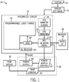
- FIG. 1 illustrates a block diagram of a system 10 that includes dynamic voltage and frequency scaling (DVFS) control circuitry.
- a designer may desire to implement functionality on an integrated circuit 12 (IC, such as a field programmable gate array (FPGA)).
- the designer may specify a high-level design 13 to be implemented, such as an OpenCL program, which may enable the designer to more efficiently and easily provide programming instructions to implement a set of programmable logic for the integrated circuit 12 without requiring specific knowledge of relatively low-level computer programming languages (e.g., Verilog or VHDL).
- OpenCL is quite similar to other high-level programming languages, such as C++, designers of programmable logic familiar with such programming languages may have a reduced learning curve than designers that are required to learn unfamiliar low programming languages to implement new functionalities in the IC.
- the designers may implement their high-level designs using design software 14, such as a version of Quartus by AlteraTM.
- the design software 14 may include Computer-Aided Design (CAD) software to aid in generation of a design configuration in the integrated circuit 12 to implement the design.
- CAD Computer-Aided Design
- the CAD software may be used in creating the design 13.
- the design software 14 may include a compiler to convert the high-level design 13 into a low-level design that may be stored in the integrated circuit 12 and/or separate memory for use in integrated circuit 12 by programming one or more gates in a programmable logic fabric 16 to cause the integrated circuit 12 to behave in a manner based at least in part on the design 13.
- FPGA performance can fluctuate based on numerous parameters, such as specific design, specific chip, temperature, voltage levels, and frequency of operation
- some CAD tools in the CAD software have been pessimistic to guarantee proper operation under worst-case conditions, such as process variation, operating temperature, noise and IR drop.
- Process variation includes manufacturing defects that can be classified as variation between devices or variation within devices. Imperfections in the fabrication process result in non-consistent dopant concentrations, oxide thickness fluctuations, stress variation, and other effects that effectively cause transistors performance to vary in the FPGA.
- the design software 14 also generates a calibration configuration for the integrated circuit 12 for determining acceptable DVFS level.
- This calibration configuration may be used to determine how the integrated circuit 12 behaves in a variety of situations by simulating or reproducing at least the critical paths of the design 13.
- the system 10 includes parameter sensor(s) 18.
- the parameter sensor(s) 18 may include temperature sensors, voltage sensing elements, frequency sensing elements, load current sensing elements, and/or other operating parameters.
- the parameter sensor(s) 18 may be located entirely on the integrated circuit 12, partly on the integrated circuit 12 and partly off-chip, or entirely off-chip. These parameter sensor(s) 18 identify DVFS parameters 20.
- one of the parameter sensor(s) 18 may be a temperature sensor that is not integrated into the integrated circuit 12, but that may identify the temperature of the integrated circuit 12 as one of the DVFS parameters 20.
- the parameter sensor(s) 18 may include error checkers that determine whether data injected in the FPGA is passed through critical paths properly under the operating conditions.
- the parameter sensor(s) 18 may determine that the integrated circuit 12 does not produce a correct result based at least in part on an adjusted supply voltage.
- the correct result may be determined from a sink register.
- the DVFS parameters 20 are passed to DVFS calibration control 22 that tracks results based on DVFS parameters 20 and whether results are proper or not. This information is stored in a DVFS calibration table (CT) 24 that is saved in memory 26 to enable the DVFS calibration control 22 to modify operating parameters of the integrated circuit 12 during operation of the integrated circuit 12 using the design 13 based at least in part on the results from the calibration stored in the calibration table 24 according to one or more parameters determined at the time of operation.
- CT DVFS calibration table
- the memory 26 may be stored in the integrated circuit 12 and/or some location outside of the integrated circuit 12, such as a host computer used to run the design software 14.
- the calibration table 24 may include a table that is a single dimension table (i.e., an array).
- the table may include voltages at which the specific design 13 functions properly within the specific integrated circuit 12 irrespective of other operating parameters.
- the calibration table 24 may include a table of values indexing more than a single parameter.
- the calibration table 24 may include indications of available voltages for a current temperature.
- the calibration table 24 may also include frequency information that indicates which voltage at the temperature may still result in correct results according to a frequency of operation.
- the voltage may be determined based at least in part on a sensed temperature and a frequency of operation.
- the frequency may also be determined based at least in part on the sensed temperature and the supply voltage.
- the DVFS calibration control 22 may send instructions to parameter control 28.
- the DVFS calibration control 22 may send a temperature control signal 30 that controls temperature modulators 32 that change a temperature under which the integrated circuit 12 is tested in a calibration phase.
- the temperature modulators 32 may be at least partially implemented outside the integrated circuit 12 as external heaters.
- the temperature modulators 32 may include heat guns.
- the temperature modulators 32 may be at least partially implemented in the integrated circuit 12.
- the temperature modulators 32 may include flip-flop chain-based logic chains configured to act as programming heaters.
- FIG. 2 illustrates a graph 34 that may be used to cycle through possible temperature levels.
- a temperature 36 may be selectable between a minimum temperature tested 38 and a maximum temperature tested 40.
- a number of temperature modulators 32 used may be increased and/or at least some of the temperature modulators 32 may produce more heat for the higher temperatures.
- the parameter control 28 may also control other parameters.
- the DVFS calibration control 22 may send a power supply control signal 42 that causes a power supply 44 to supply a voltage 48 Vcore to the integrated circuit 12.
- FIG. 3A illustrates a graph 46 of voltages through which the power supply 44 may cycle through during the calibration. For example, each cycle may be deployed at each temperature to be tested between the minimum temperature tested 38 and the maximum temperature tested 40.
- the voltage 48 is gradually reduced to a minimum working voltage 50. In some embodiments, the voltage 48 is reduced until the system experiences an error, and the last error-free voltage is set as the minimum working voltage 50. In some embodiments, the voltage 48 may then be increased while modifying other parameters, such as frequency of operation for the system.
- 3B illustrates a graph 52 of system frequency 56 that is increased at each voltage until an error occurs.
- the system frequency 56 may be the frequency of a clock 58 of FIG. 1 that is used to control operation of the integrated circuit 12.
- corresponding error-free frequencies 56 may be stored in the calibration table 24.
- the voltages 48 and corresponding error-free frequencies 56 working frequencies may be determined and stored for each temperature level to be tested as indicated in FIG. 2 .
- the integrated circuit 12 also includes IO blocks 60 that may be used to write data to the integrated circuit 12 and/or read data from the integrated circuit 12.
- the integrated circuit 12 may also include hard blocks such as random accessible memory (RAM) blocks, digital signal processing (DSP) blocks, and/or other logical blocks that may be included in the calibration configuration to determine when these blocks fail due to certain parameters (e.g., voltage, current draw) in certain modes that cause the system to be unable to function properly for certain parameters.
- the calibration table 24 will track these values as well as those that do not rely on the hard blocks.
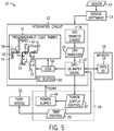
- FIG. 4 illustrates a schematic view of the system 10 illustrating temperature modulators 32 distributed throughout the programmable logic fabric.
- the temperature modulators 32 are located on the integrated circuit 12 as heaters 70 that are distributed throughout the integrated circuit 12.
- the heaters 70 may include flip-flop chain-based logic chains in the programmable logic fabric 16.
- a number of heaters 70 used to heat the die of the integrated circuit 12 may vary according to the temperature 36 of FIG. 2 .
- the heaters 70 may be used to achieve each of the temperatures through which the calibration is performed.
- the heaters 70 may be any circuitry that is not used for critical paths 72 that are used to simulate or replicate paths that are to be used by the design 13 during usage of the integrated circuit 12.
- the critical paths 72 include one or more gates that are used in that would be expected to result in a longest overall duration.
- Each critical path includes error checking 76 determining whether the critical path 72 functions properly at the current operating conditions. However, measuring information based only on a most critical path is less robust than testing less critical paths since most-critical-path-only testing ignores within-die variation. Thus, calibration procedures may be executed using one or more critical paths. The number of critical paths to be used may be determined based on the specific design. For example, FIG. 5 illustrates an embodiment of the integrated circuit 12 with additional less-critical paths 78. Each additional path to be tested during calibration increases calibration duration but increases flexibility and possibility of power reduction and/or enhanced performance.
- FIG. 6 illustrates a flow diagram view of a process 80 for generating calibration configuration(s) for calibrating the integrated circuit 12 to enhance performance and power savings.
- the design software 14 running on a host computer or other device obtains top critical path information 82 for a number of critical paths in the design 13 (block 82). For a number of these paths, the design software 14 replicates the paths in a calibration configuration (block 84). Replication may also include creating additional components for each path including exercise, sensitization, and error detection components. The exercise components inject data into the critical paths, sensitization determines results of the data after passing through the critical paths, and the error detection components determine whether the critical paths react to the data properly. As discussed above, a higher number of paths increases obtained information and potential power savings and/or enhanced performance.
- the design software 14 determines whether the current critical path fits into the calibration configuration (block 86).
- the calibration configuration may include more than a single configuration. If all critical paths to be included in the calibration are able to fit into a single configuration with corresponding exercise, sensitization, and error detection components for each critical path, a single calibration configuration may be deployed. However, if the critical paths cannot physically coexist in the FPGA, the critical paths may be stored in multiple configurations. Multiple configurations also increases a calibration duration but provides reliable results that single out each path determining whether each critical path 72 is functioning properly at the operating conditions. If the critical path 72 is to be tested but cannot fit into a current configuration, checking the next configuration includes creating a new calibration configuration.
- the design software 14 determines whether each of the critical paths has been replicated in a calibration configuration (block 90). If not, the design software 14 replicates the remaining critical paths to be tested in a calibration configuration. If all critical paths to be tested have been included, the calibration of the integrated circuit 12 may be performed using the one or more calibration configurations (block 92).
- FIG. 7 illustrates a process 100 for dynamically varying a parameter of operation of the system 10.
- the process 100 includes generating one or more calibration configurations using the design software 14 (block 102).
- the calibration configurations may be generated using the process 80 previously discussed.
- the DVFS calibration control 22 runs a calibration using the calibration configurations.
- the DVFS calibration control 22 may determine, for each temperature tested, a minimum working voltage and a maximum frequency at each voltage, as previously discussed in reference to FIGS. 3A & 3B . Additionally or alternatively, the DVFS calibration control 22 may determine a lowest voltage possible for each frequency at each temperature tested.
- the DVFS calibration control 22 may track additional parameters, such as current from the power supply either as average current and/or transient current.
- the DVFS calibration control 22 may also track the frequency of the transiency of the current.
- the DVFS calibration control 22 tracks this information and stores it in the calibration table (CT) 24 (block 106).
- the calibration table 24 may include a lookup table that indicates minimum and/or maximum voltage, temperature of die, frequency of the clock, transient and/or average current of the power supply, frequency of transiency of the current of the power supply, and/or other operating parameters of the integrated circuit 12 as a table having one or more dimensions.
- the DVFS calibration control 22 operates the integrated circuit 12 using the design 13 to reduce power consumption of the integrated circuit 12 during operation.
- FIG. 8 illustrates a detailed flow diagram view of a process 120 for dynamically varying temperature, voltage, and frequency.
- the FPGA is set to one of a number of calibration configurations to be tested (block 122).
- the calibration configurations may be determined using the process 80 of FIG. 6 .
- a temperature for the die to be tested is set (block 124).
- the DVFS calibration control 22 may cause a number of heaters 70 to be set to achieve a desired temperature.
- the initial temperature may be a base temperature that not elevated by any of the heaters. In other words, the initial temperature may be that which is achieved without additional heating.
- the DVFS calibration control 22 can verify what the initial temperature is by using the DVFS parameter sensor(s) 18 to determine the temperature as a DVFS parameter 20.
- the DVFS calibration control 22 also sets voltage and frequency to initial values (block 126).
- the initial voltage may be a pessimistic voltage that is likely to cause the integrated circuit 12 to function properly even in worst-case scenarios of temperature and frequency.
- the frequency may be similarly selected as a pessimistic worst-case scenario for temperature and the initial voltage.
- the voltage then is reduced incrementally (block 128).
- the DVFS calibration control 22 tracks whether an error has been detected (block 130). For example, the DVFS calibration control 22 may track when an error signal is received from the error checkers. Specifically, when data at the error checkers 76 does not match expected results from data injected into a respective critical path 72.
- the current voltage may be stored in the calibration table 24 as the lowest voltage for the current temperature (block 132).
- the lowest voltage may be stored relative to the temperature and the frequency.
- the lowest voltage may not be stored for each voltage that is error-free, and instead, only the last lowest working voltage is stored after the first failing voltage occurs.
- a lowest working voltage may be automatically set to some voltage or may be cut off at some threshold where even best-case scenarios are likely to fail.
- storing the lowest voltage causes the calibration table to mark all voltages below the lowest voltage as impermissible for the temperature and all voltages above as permissible.
- the lowest voltage and the highest voltage may both be determined for the temperature and all voltages outside this range are deemed as error-prone voltages.
- the DVFS calibration control 22 cycles through frequency values of the clock 58 to determine a fastest clock that is error-free for the current voltage and temperature. To this end, the DVFS calibration control 22 increments the frequency (block 134) until an error is detected or a maximum frequency threshold has been surpassed (block 136).
- the maximum frequency threshold may correspond to a maximum desired frequency due to constraints on the system 10 such as physical limitations of the integrated circuit 12 and/or the clock 58.
- the highest and last working frequency may be set in the calibration table 24 as corresponding to the temperature and current (block 138). Also similar to the lowest voltage, the highest frequency may be stored as each frequency is tested or only written as the last working frequency when a first error is detected at the next frequency tested.
- storing the highest frequency causes the calibration table to mark all frequencies above the highest frequency as impermissible for the temperature and voltage and all frequencies below as permissible frequencies (though some frequencies below a slower threshold may be deemed impermissible as slowing the FPGA to an undesireable extent.
- the CVFS calibration controller 22 determines if more voltages are to be tested (block 140). This determination may be made based on whether the calibration table 24 is fully populated for the current temperature and/or if a previous voltage worked for at least some frequencies, the next frequency may be tested. If more voltages are to be tested, the voltage is incremented and the frequency is reset to the initial value (block 142). However, if no voltages are to be tested, the CVFS calibration control 22 determines whether additional temperatures are to be tested (block 144).
- the additional temperature determination may be based on whether the calibration table 24 is fully populated and/or if a previous temperature worked for at least some voltages, the next frequency may be tested. Once all temperatures have been tested, a determination is made whether additional configurations are to be tested (block 148). Specifically, if all critical paths to be tested cannot be tested in parallel, more than one generated calibration configuration may exist. If another configuration is to be tested, the next configuration is selected 150, and the process 120 begins again for the new calibration configuration.
- the FPGA is set to the design configuration (block 152).
- the FPGA is then ready to operate in the design configuration based at least in part on the calibration table 24 and measured operating conditions (block 154).
- the calibration table 24 may be modified by some guardband to ensure that any operating parameters are more likely to result in proper operation of the integrated circuit 12.
- the guardband may include 5% modulators the increase or decrease acceptable conditions, such as an increase to voltage and/or a decrease in frequency at specific temperatures.
- this modulation of the values in the calibration table 24 may include other modulated values, such as 1%, 2%, 3%, 4%, or more than 5%.
- the guardband may be determined dynamically by the design software 14 based on analysis of the worst-case variation in a critical path due to parameters such as crosstalk that may not be calibrated (e.g., cannot be repetitively reproduced). The analysis takes into account an amount of delay variation that is due to crosstalk on each path and a corresponding timing slack to produce a guardband. For example, the design software 14 may determine a maximum delay variation for all critical paths of the design 13.
- process 120 may split voltage and frequency scans into separate cycles by cycling through each voltage for each temperature in a first past and a second pass of each frequency for each temperature and voltage.
- temperature, voltage, and frequency cycling in such order, have been discussed above for clarity, but any parameters that affect integrated circuit 12 operation may be tested in such a manner.
- the temperature, voltage, and frequency may each respectively be replaced by or supplemented with minimum and/or maximum voltage, temperature of die, frequency of the clock, transient and/or average current of the power supply, frequency of transiency of the current of the power supply, and/or other operating parameters even including rearrangement of the testing of the temperature, voltage, and frequency.
Landscapes
- Physics & Mathematics (AREA)
- Mathematical Physics (AREA)
- Engineering & Computer Science (AREA)
- Computer Hardware Design (AREA)
- General Engineering & Computer Science (AREA)
- Computing Systems (AREA)
- Computer Networks & Wireless Communication (AREA)
- Theoretical Computer Science (AREA)
- Evolutionary Computation (AREA)
- Geometry (AREA)
- General Physics & Mathematics (AREA)
- Semiconductor Integrated Circuits (AREA)
Claims (15)
- Integrierte Schaltung (12), die aufweist:eine programmierbare Logik-Fabric (16), die mit einer Kalibrierungskonfiguration ausgebildet ist, die einen Nachbildungspfad für jeden von einem oder mehreren kritischen Pfaden in einer Betriebsgestaltung (13) für die programmierbare Logik-Fabric (16) enthält, wobei die Kalibrierungskonfiguration ferner Fehlerprüfer enthält, die bestimmen, ob in die programmierbare Logik-Fabric (16) eingespeiste Daten unter der Betriebsbedingung ordnungsgemäß durch den einen oder die mehreren Nachbildungspfade geleitet werden; undeine Steuereinrichtung (22) für dynamische Parameterskalierung, die dazu ausgebildet ist:während eines Kalibrierungsmodus einen ersten Betriebsparameter der programmierbaren Logik-Fabric (16) bei einem gegebenen Wert beizubehalten, während Werte mindestens eines weiteren Betriebsparameters der programmierbaren Logik-Fabric (16) durchlaufen werden, wobei damit unter Verwendung der Fehlerprüfer bestimmt wird, dass ein oder mehrere funktionelle Werte eines oder mehrerer weiterer Betriebsparameter der programmierbaren Logik-Fabric (16), bei denen Daten, die in die programmierbare Logik-Fabric (16) eingespeist werden, durch den einen oder die mehreren Nachbildungspfade geleitet werden, ordnungsgemäß funktionieren;den einen oder die mehreren funktionellen Werte für den einen oder die mehreren weiteren Betriebsparameter in einer Kalibrierungstabelle (24) zu speichern; unddie programmierbare Logik-Fabric (16), wenn sie unter Verwendung der Gestaltungskonfiguration (13) betrieben wird, unter Verwendung des einen oder der mehreren funktionellen Werte für den einen oder die mehreren weiteren Betriebsparameter in einer Kalibrierungstabelle (24) zu betreiben.
- Integrierte Schaltung (12) nach Anspruch 1, wobei der erste Betriebsparameter eine Temperatur der programmierbaren Logik-Fabric (16) ist.
- Integrierte Schaltung (12) nach Anspruch 2, wobei die Steuereinrichtung (22) für dynamische Parameterskalierung dazu ausgebildet ist, einen Temperaturwert zu inkrementieren (146), bis eine Temperaturschwelle erreicht ist, und die Werte des mindestens einen weiteren Betriebsparameters der programmierbaren Logik-Fabric (16) für jeden inkrementierten Temperaturwert zu durchlaufen.
- Integrierte Schaltung (12) nach einem der Ansprüche 1 bis 3, wobei der mindestens eine weitere Betriebsparameter der programmierbaren Logik-Fabric (16) einen Spannungswert umfasst.
- Integrierte Schaltung (12) nach Anspruch 4, wobei das Durchlaufen der Werte mindestens eines weiteren Betriebsparameters der programmierbaren Logik-Fabric (16) das inkrementelle Reduzieren (128) des Spannungswerts umfasst.
- Integrierte Schaltung (12) nach Anspruch 5, wobei das Speichern (132) des einen oder der mehreren funktionellen Werte in der Kalibrierungstabelle (24) das Angeben umfasst, ob ein Spannungswert bei einem speziellen Wert für den ersten Betriebsparameter funktionell ist.
- Integrierte Schaltung (12) nach Anspruch 5, wobei das Speichern (132) des einen oder der mehreren funktionellen Werte in der Kalibrierungstabelle (24) das Speichern eines niedrigsten Spannungswerts umfasst, der bei einem speziellen Wert für den ersten Betriebsparameter funktionell ist.
- Integrierte Schaltung (12) nach einem der Ansprüche 1 bis 7, wobei die Steuereinrichtung (22) für dynamische Parameterskalierung dazu ausgebildet ist, funktionelle Werte der Betriebsparameter in der Kalibrierungstabelle (24) zu modifizieren, um ein Sicherheitsband zu implementieren, das den gespeicherten einen oder die gespeicherten mehreren funktionellen Werte durch Erhöhen oder Verringern eines oder mehrerer funktioneller Werte weg von einer Fehlerzustandsrichtung modifiziert.
- Integrierte Schaltung (12) nach Anspruch 8, wobei das Sicherheitsband einen konsistenten Modifiziererprozentsatz umfasst, der den einen oder die mehreren funktionellen Werte um einen Prozentsatz des funktionellen Werts modifiziert.
- Integriertes Schaltungssystem nach einem der Ansprüche 1 bis 9, wobei der mindestens eine weitere Betriebsparameter der programmierbaren Logik-Fabric (16) einen Frequenzwert umfasst, der eine Frequenz des Betriebs der programmierbaren Logik-Fabric (16) angibt.
- Verfahren (100) zum Betreiben einer programmierbaren Logik-Fabric (16) in einer integrierten Schaltung (12) unter Verwendung dynamischer Parameterskalierung, wobei das Verfahren umfasst:Analysieren einer Gestaltungskonfiguration (13) der programmierbaren Logik-Fabric (16) der integrierten Schaltung (12), um kritische Pfade in der Gestaltungskonfiguration (13) zu bestimmen (82),Erzeugen (84, 102) einer Kalibrierungskonfiguration, die einen Nachbildungspfad für jeden von einem oder mehreren der kritischen Pfade in der Betriebsgestaltung (13) enthält, wobei die Kalibrierungskonfiguration ferner Fehlerprüfer enthält, die bestimmen, ob in die programmierbare Logik-Fabric (16) eingespeiste Daten unter der Betriebsbedingung ordnungsgemäß durch den einen oder die mehreren Nachbildungspfade geleitet werden;während eines Kalibrierungsmodus Betreiben (122) der programmierbaren Logik-Fabric (16) unter Verwendung der Kalibrierungskonfiguration und Beibehalten (124) eines ersten Betriebsparameters der programmierbaren Logik-Fabric (16) bei einem gegebenen Wert, während mögliche Werte mindestens eines weiteren Betriebsparameters der programmierbaren Logik-Fabric (16) durchlaufen werden (128, 130, ..., 142), wobei damit bestimmt wird, dass ein oder mehrere funktionelle Werte eines oder mehrerer weiterer Betriebsparameter der programmierbaren Logik-Fabric (16), bei denen Daten, die in die programmierbare Logik-Fabric (16) eingespeist werden, durch den einen oder die mehreren kritischen Pfade geleitet werden, ordnungsgemäß funktionieren, und Speichern (132, 138) des einen oder der mehreren funktionellen Werte für den einen oder die mehreren weiteren Betriebsparameter in einer Kalibrierungstabelle (24); undBetreiben (152, 154) der programmierbaren Logik-Fabric (16) unter Verwendung der Gestaltungskonfiguration (13) und unter Verwendung des einen oder der mehreren funktionellen Werte für den einen oder die mehreren weiteren Betriebsparameter, die in der Kalibrierungstabelle (24) gespeichert sind.
- Verfahren nach Anspruch 11, wobei die Betriebsparameter Temperatur, Spannung und Frequenz des Betriebs der programmierbaren Logik-Fabric (16) umfassen.
- Verfahren nach Anspruch 12, wobei die Betriebsparameter eines oder mehrere umfassen von einer Frequenz eines Taktgebers (58) der programmierbaren Logik-Fabric (16), einem transienten und/oder durchschnittlichen Strom einer Energieversorgung (44) der integrierten Schaltung (12) und einer Frequenz der Transienz eines Stroms der Energieversorgung (44).
- Verfahren nach Anspruch 11 oder 12, wobei das Erzeugen der Kalibrierungskonfiguration (84, 102) das Erzeugen einer Mehrzahl von Kalibrierungskonfigurationen umfasst.
- Verfahren nach Anspruch 14, wobei das Erzeugen der Mehrzahl von Kalibrierungskonfigurationen umfasst:
für eine Anzahl kritischer Pfade, die sich von dem Analysieren der Gestaltungskonfiguration (13) der programmierbaren Logik-Fabric (16) der integrierten Schaltung (12) ableiten:Bestimmen, ob jeder jeweilige kritische Pfad der Anzahl kritischer Pfade in eine erste Kalibrierungskonfiguration der Mehrzahl von Kalibrierungskonfigurationen passt;wenn der jeweilige kritische Pfad in die erste Kalibrierungskonfiguration passt, Hinzufügen eines oder mehrerer kritischer Pfade zu der ersten Kalibrierungskonfiguration; undwenn der jeweilige kritische Pfad nicht in die erste Kalibrierungskonfiguration passt, Hinzufügen eines oder mehrerer kritischer Pfade zu einer folgenden Kalibrierungskonfiguration der Mehrzahl von Kalibrierungskonfigurationen.
Applications Claiming Priority (3)
| Application Number | Priority Date | Filing Date | Title |
|---|---|---|---|
| US201662310565P | 2016-03-18 | 2016-03-18 | |
| US15/199,329 US20170272073A1 (en) | 2016-03-18 | 2016-06-30 | Dynamic parameter operation of an fpga |
| PCT/US2017/017495 WO2017160434A1 (en) | 2016-03-18 | 2017-02-10 | Dynamic parameter operation of an fpga |
Publications (3)
| Publication Number | Publication Date |
|---|---|
| EP3430544A1 EP3430544A1 (de) | 2019-01-23 |
| EP3430544A4 EP3430544A4 (de) | 2019-12-11 |
| EP3430544B1 true EP3430544B1 (de) | 2021-03-24 |
Family
ID=59847193
Family Applications (1)
| Application Number | Title | Priority Date | Filing Date |
|---|---|---|---|
| EP17767125.2A Active EP3430544B1 (de) | 2016-03-18 | 2017-02-10 | Dynamische parameteroperation eines fpga |
Country Status (4)
| Country | Link |
|---|---|
| US (1) | US20170272073A1 (de) |
| EP (1) | EP3430544B1 (de) |
| CN (1) | CN108780469B (de) |
| WO (1) | WO2017160434A1 (de) |
Families Citing this family (17)
| Publication number | Priority date | Publication date | Assignee | Title |
|---|---|---|---|---|
| DE102015118129A1 (de) * | 2015-10-23 | 2017-04-27 | Dspace Digital Signal Processing And Control Engineering Gmbh | Verfahren zum Ermitteln der Leistungsaufnahme eines programmierbaren Logikbausteins |
| US11334696B2 (en) * | 2017-09-28 | 2022-05-17 | Intel Corporation | Systems and methods for dynamic voltage and frequency scaling in programmable logic devices |
| WO2019136299A1 (en) | 2018-01-05 | 2019-07-11 | Atlazo, Inc. | Power management system |
| US10614184B2 (en) | 2018-01-08 | 2020-04-07 | Atlazo, Inc. | Semiconductor process and performance sensor |
| US10416746B2 (en) * | 2018-01-10 | 2019-09-17 | Atlazo, Inc. | Adaptive energy optimal computing |
| US10635130B2 (en) | 2018-02-01 | 2020-04-28 | Atlazo, Inc. | Process, voltage and temperature tolerant clock generator |
| US10571945B2 (en) | 2018-02-21 | 2020-02-25 | Atlazo, Inc. | Low power regulator circuits, systems and methods regarding the same |
| US10732699B2 (en) * | 2018-02-23 | 2020-08-04 | Intel Corporation | Redundancy in distribution of voltage-frequency scaling parameters |
| US10700604B2 (en) | 2018-03-07 | 2020-06-30 | Atlazo, Inc. | High performance switch devices and methods for operating the same |
| JP2020057690A (ja) * | 2018-10-02 | 2020-04-09 | ルネサスエレクトロニクス株式会社 | 半導体装置及び電圧設定方法 |
| US11709275B2 (en) * | 2019-07-09 | 2023-07-25 | Xilinx, Inc. | Root monitoring on an FPGA using satellite ADCs |
| KR102817702B1 (ko) * | 2019-07-09 | 2025-06-05 | 자일링크스 인코포레이티드 | 위성 adc를 사용한 fpga의 루트 모니터링 |
| US10598729B1 (en) * | 2019-08-08 | 2020-03-24 | Xilinx, Inc. | Device monitoring using satellite ADCs having local voltage reference |
| US11271581B1 (en) | 2020-05-18 | 2022-03-08 | Xilinx, Inc. | Time-multiplexed distribution of analog signals |
| US12273107B2 (en) * | 2021-12-22 | 2025-04-08 | Altera Corporation | Dynamically scalable timing and power models for programmable logic devices |
| US12437135B2 (en) * | 2021-12-22 | 2025-10-07 | Altera Corporation | Dynamic loadlines for programmable fabric devices |
| CN115062571B (zh) * | 2022-05-06 | 2024-12-06 | 上海概伦电子股份有限公司 | 应用于集成电路器件的数据区域动态选取方法、系统、设备和计算机可读存储介质 |
Family Cites Families (19)
| Publication number | Priority date | Publication date | Assignee | Title |
|---|---|---|---|---|
| US6769107B1 (en) * | 2001-12-03 | 2004-07-27 | Lsi Logic Corporation | Method and system for implementing incremental change to circuit design |
| US7814350B2 (en) * | 2002-10-03 | 2010-10-12 | Via Technologies, Inc. | Microprocessor with improved thermal monitoring and protection mechanism |
| GB2410344B (en) * | 2004-01-26 | 2006-03-15 | Toshiba Res Europ Ltd | Dynamic voltage controller |
| US7649374B2 (en) * | 2005-09-15 | 2010-01-19 | Finisar Corporation | Temperature control in an integrated circuit |
| US7444181B2 (en) * | 2005-12-14 | 2008-10-28 | Boston Scientific Neuromodulation Corporation | Techniques for sensing and adjusting a compliance voltage in an implantable stimulator device |
| US8102187B2 (en) * | 2008-05-02 | 2012-01-24 | Texas Instruments Incorporated | Localized calibration of programmable digital logic cells |
| US9081501B2 (en) * | 2010-01-08 | 2015-07-14 | International Business Machines Corporation | Multi-petascale highly efficient parallel supercomputer |
| TW201140308A (en) * | 2010-03-15 | 2011-11-16 | Kyushu Inst Technology | Semiconductor device, detection method, and program |
| US9015023B2 (en) * | 2010-05-05 | 2015-04-21 | Xilinx, Inc. | Device specific configuration of operating voltage |
| US8736674B2 (en) * | 2010-09-23 | 2014-05-27 | Dolby Laboratories Licensing Corporation | Method and system for 3D display calibration with feedback determined by a camera device |
| US8904115B2 (en) * | 2010-09-28 | 2014-12-02 | Texas Instruments Incorporated | Cache with multiple access pipelines |
| US8750065B2 (en) * | 2011-06-28 | 2014-06-10 | Rochester Institute Of Technology | Thermal management apparatuses with temperature sensing resistive random access memory devices and methods thereof |
| EP2549482B1 (de) * | 2011-07-22 | 2018-05-23 | SanDisk Technologies LLC | Vorrichtung, System und Verfahren zur Bestimmung einer Parameterkonfiguration für Solid-State Speichervorrichtungen. |
| US8698516B2 (en) * | 2011-08-19 | 2014-04-15 | Altera Corporation | Apparatus for improving performance of field programmable gate arrays and associated methods |
| US9342403B2 (en) * | 2014-03-28 | 2016-05-17 | Intel Corporation | Method and apparatus for managing a spin transfer torque memory |
| US9276563B2 (en) * | 2014-06-13 | 2016-03-01 | International Business Machines Corporation | Clock buffers with pulse drive capability for power efficiency |
| US20160054374A1 (en) * | 2014-08-20 | 2016-02-25 | Darryl G. Walker | Semiconductor device including temperature ranges having temperature thresholds and method of determining therefor |
| US9413344B2 (en) * | 2014-09-08 | 2016-08-09 | Qualcomm Incorporated | Automatic calibration circuits for operational calibration of critical-path time delays in adaptive clock distribution systems, and related methods and systems |
| US9618999B1 (en) * | 2015-11-17 | 2017-04-11 | International Business Machines Corporation | Idle-aware margin adaption |
-
2016
- 2016-06-30 US US15/199,329 patent/US20170272073A1/en not_active Abandoned
-
2017
- 2017-02-10 CN CN201780012033.XA patent/CN108780469B/zh active Active
- 2017-02-10 WO PCT/US2017/017495 patent/WO2017160434A1/en not_active Ceased
- 2017-02-10 EP EP17767125.2A patent/EP3430544B1/de active Active
Non-Patent Citations (1)
| Title |
|---|
| None * |
Also Published As
| Publication number | Publication date |
|---|---|
| WO2017160434A1 (en) | 2017-09-21 |
| EP3430544A1 (de) | 2019-01-23 |
| CN108780469A (zh) | 2018-11-09 |
| CN108780469B (zh) | 2023-09-05 |
| US20170272073A1 (en) | 2017-09-21 |
| EP3430544A4 (de) | 2019-12-11 |
Similar Documents
| Publication | Publication Date | Title |
|---|---|---|
| EP3430544B1 (de) | Dynamische parameteroperation eines fpga | |
| US9536038B1 (en) | Method and algorithm for functional critical paths selection and critical path sensors and controller insertion | |
| US7983870B2 (en) | Integrated circuit and method for determining the operating range of an integrated circuit | |
| JP5586780B2 (ja) | デバイスの動作電圧の仕様構成 | |
| CN104135256A (zh) | 一种带自校准功能的延时采样电路 | |
| US11334696B2 (en) | Systems and methods for dynamic voltage and frequency scaling in programmable logic devices | |
| KR101773490B1 (ko) | 데이터-의존 회로 경로 응답들을 이용하는 고유하고 복제불가한 플랫폼 식별자들 | |
| KR102170198B1 (ko) | 전력 공급 모니터를 사용하여 전력 공급 교정 | |
| US20080133155A1 (en) | Method and apparatus to generate circuit energy models with multiple clock gating inputs | |
| US8008967B2 (en) | Power supply voltage adjusting device | |
| US10615802B2 (en) | Dynamic parameter operation of an FPGA | |
| CN106570210A (zh) | 电路设计方法、电路仿真方法和基于计算机的仿真系统 | |
| Zhao et al. | A universal self-calibrating dynamic voltage and frequency scaling (dvfs) scheme with thermal compensation for energy savings in fpgas | |
| US8510692B2 (en) | Verification system and method using constrained random test parameter selection | |
| US7546566B2 (en) | Method and system for verification of multi-voltage circuit design | |
| US9021324B2 (en) | Calibration arrangement | |
| US8146041B1 (en) | Latch based optimization during implementation of circuit designs for programmable logic devices | |
| CN104849647A (zh) | 对于电路可靠性老化的方法和装置 | |
| Nunez-Yanez | Energy proportional computing in commercial FPGAs with adaptive voltage scaling | |
| JP2009086848A (ja) | 半導体装置、半導体装置の制御方法および半導体装置の制御情報の作成方法 | |
| US7346866B2 (en) | Method and apparatus to generate circuit energy models with clock gating | |
| KR100809684B1 (ko) | 디바이스의 전원차단효과를 rtl에서 검증할 수 있는 검증 장치 및 전원차단효과를 모델링 하는 방법 | |
| Pecorella | All-Digital Noise-Tolerant Voltage-Level Detector for Dynamic Configuration of SRAM Read/Write-Assist Circuits | |
| Niemann et al. | Sensor based adaptive voltage scaling on fpgas: Calibration and parametrization | |
| US20250335678A1 (en) | Determining an operational limit for a circuit component |
Legal Events
| Date | Code | Title | Description |
|---|---|---|---|
| STAA | Information on the status of an ep patent application or granted ep patent |
Free format text: STATUS: THE INTERNATIONAL PUBLICATION HAS BEEN MADE |
|
| PUAI | Public reference made under article 153(3) epc to a published international application that has entered the european phase |
Free format text: ORIGINAL CODE: 0009012 |
|
| STAA | Information on the status of an ep patent application or granted ep patent |
Free format text: STATUS: REQUEST FOR EXAMINATION WAS MADE |
|
| 17P | Request for examination filed |
Effective date: 20180815 |
|
| AK | Designated contracting states |
Kind code of ref document: A1 Designated state(s): AL AT BE BG CH CY CZ DE DK EE ES FI FR GB GR HR HU IE IS IT LI LT LU LV MC MK MT NL NO PL PT RO RS SE SI SK SM TR |
|
| AX | Request for extension of the european patent |
Extension state: BA ME |
|
| DAV | Request for validation of the european patent (deleted) | ||
| DAX | Request for extension of the european patent (deleted) | ||
| A4 | Supplementary search report drawn up and despatched |
Effective date: 20191111 |
|
| RIC1 | Information provided on ipc code assigned before grant |
Ipc: H03K 19/177 20060101ALI20191105BHEP Ipc: G06F 17/50 20060101AFI20191105BHEP Ipc: H03K 19/003 20060101ALI20191105BHEP |
|
| REG | Reference to a national code |
Ref country code: DE Ref legal event code: R079 Ref document number: 602017035281 Country of ref document: DE Free format text: PREVIOUS MAIN CLASS: G06F0017500000 Ipc: G06F0030340000 |
|
| RIC1 | Information provided on ipc code assigned before grant |
Ipc: G06F 30/34 20200101AFI20200630BHEP |
|
| GRAP | Despatch of communication of intention to grant a patent |
Free format text: ORIGINAL CODE: EPIDOSNIGR1 |
|
| STAA | Information on the status of an ep patent application or granted ep patent |
Free format text: STATUS: GRANT OF PATENT IS INTENDED |
|
| INTG | Intention to grant announced |
Effective date: 20200901 |
|
| GRAS | Grant fee paid |
Free format text: ORIGINAL CODE: EPIDOSNIGR3 |
|
| GRAA | (expected) grant |
Free format text: ORIGINAL CODE: 0009210 |
|
| STAA | Information on the status of an ep patent application or granted ep patent |
Free format text: STATUS: THE PATENT HAS BEEN GRANTED |
|
| AK | Designated contracting states |
Kind code of ref document: B1 Designated state(s): AL AT BE BG CH CY CZ DE DK EE ES FI FR GB GR HR HU IE IS IT LI LT LU LV MC MK MT NL NO PL PT RO RS SE SI SK SM TR |
|
| REG | Reference to a national code |
Ref country code: GB Ref legal event code: FG4D |
|
| REG | Reference to a national code |
Ref country code: CH Ref legal event code: EP |
|
| REG | Reference to a national code |
Ref country code: IE Ref legal event code: FG4D |
|
| REG | Reference to a national code |
Ref country code: DE Ref legal event code: R096 Ref document number: 602017035281 Country of ref document: DE Ref country code: AT Ref legal event code: REF Ref document number: 1375224 Country of ref document: AT Kind code of ref document: T Effective date: 20210415 |
|
| REG | Reference to a national code |
Ref country code: NL Ref legal event code: FP |
|
| REG | Reference to a national code |
Ref country code: LT Ref legal event code: MG9D |
|
| PG25 | Lapsed in a contracting state [announced via postgrant information from national office to epo] |
Ref country code: FI Free format text: LAPSE BECAUSE OF FAILURE TO SUBMIT A TRANSLATION OF THE DESCRIPTION OR TO PAY THE FEE WITHIN THE PRESCRIBED TIME-LIMIT Effective date: 20210324 Ref country code: HR Free format text: LAPSE BECAUSE OF FAILURE TO SUBMIT A TRANSLATION OF THE DESCRIPTION OR TO PAY THE FEE WITHIN THE PRESCRIBED TIME-LIMIT Effective date: 20210324 Ref country code: GR Free format text: LAPSE BECAUSE OF FAILURE TO SUBMIT A TRANSLATION OF THE DESCRIPTION OR TO PAY THE FEE WITHIN THE PRESCRIBED TIME-LIMIT Effective date: 20210625 Ref country code: NO Free format text: LAPSE BECAUSE OF FAILURE TO SUBMIT A TRANSLATION OF THE DESCRIPTION OR TO PAY THE FEE WITHIN THE PRESCRIBED TIME-LIMIT Effective date: 20210624 Ref country code: BG Free format text: LAPSE BECAUSE OF FAILURE TO SUBMIT A TRANSLATION OF THE DESCRIPTION OR TO PAY THE FEE WITHIN THE PRESCRIBED TIME-LIMIT Effective date: 20210624 |
|
| PG25 | Lapsed in a contracting state [announced via postgrant information from national office to epo] |
Ref country code: RS Free format text: LAPSE BECAUSE OF FAILURE TO SUBMIT A TRANSLATION OF THE DESCRIPTION OR TO PAY THE FEE WITHIN THE PRESCRIBED TIME-LIMIT Effective date: 20210324 Ref country code: LV Free format text: LAPSE BECAUSE OF FAILURE TO SUBMIT A TRANSLATION OF THE DESCRIPTION OR TO PAY THE FEE WITHIN THE PRESCRIBED TIME-LIMIT Effective date: 20210324 Ref country code: SE Free format text: LAPSE BECAUSE OF FAILURE TO SUBMIT A TRANSLATION OF THE DESCRIPTION OR TO PAY THE FEE WITHIN THE PRESCRIBED TIME-LIMIT Effective date: 20210324 |
|
| REG | Reference to a national code |
Ref country code: AT Ref legal event code: MK05 Ref document number: 1375224 Country of ref document: AT Kind code of ref document: T Effective date: 20210324 |
|
| PG25 | Lapsed in a contracting state [announced via postgrant information from national office to epo] |
Ref country code: LT Free format text: LAPSE BECAUSE OF FAILURE TO SUBMIT A TRANSLATION OF THE DESCRIPTION OR TO PAY THE FEE WITHIN THE PRESCRIBED TIME-LIMIT Effective date: 20210324 Ref country code: EE Free format text: LAPSE BECAUSE OF FAILURE TO SUBMIT A TRANSLATION OF THE DESCRIPTION OR TO PAY THE FEE WITHIN THE PRESCRIBED TIME-LIMIT Effective date: 20210324 Ref country code: CZ Free format text: LAPSE BECAUSE OF FAILURE TO SUBMIT A TRANSLATION OF THE DESCRIPTION OR TO PAY THE FEE WITHIN THE PRESCRIBED TIME-LIMIT Effective date: 20210324 Ref country code: SM Free format text: LAPSE BECAUSE OF FAILURE TO SUBMIT A TRANSLATION OF THE DESCRIPTION OR TO PAY THE FEE WITHIN THE PRESCRIBED TIME-LIMIT Effective date: 20210324 Ref country code: AT Free format text: LAPSE BECAUSE OF FAILURE TO SUBMIT A TRANSLATION OF THE DESCRIPTION OR TO PAY THE FEE WITHIN THE PRESCRIBED TIME-LIMIT Effective date: 20210324 |
|
| PG25 | Lapsed in a contracting state [announced via postgrant information from national office to epo] |
Ref country code: IS Free format text: LAPSE BECAUSE OF FAILURE TO SUBMIT A TRANSLATION OF THE DESCRIPTION OR TO PAY THE FEE WITHIN THE PRESCRIBED TIME-LIMIT Effective date: 20210724 Ref country code: SK Free format text: LAPSE BECAUSE OF FAILURE TO SUBMIT A TRANSLATION OF THE DESCRIPTION OR TO PAY THE FEE WITHIN THE PRESCRIBED TIME-LIMIT Effective date: 20210324 Ref country code: RO Free format text: LAPSE BECAUSE OF FAILURE TO SUBMIT A TRANSLATION OF THE DESCRIPTION OR TO PAY THE FEE WITHIN THE PRESCRIBED TIME-LIMIT Effective date: 20210324 Ref country code: PT Free format text: LAPSE BECAUSE OF FAILURE TO SUBMIT A TRANSLATION OF THE DESCRIPTION OR TO PAY THE FEE WITHIN THE PRESCRIBED TIME-LIMIT Effective date: 20210726 Ref country code: PL Free format text: LAPSE BECAUSE OF FAILURE TO SUBMIT A TRANSLATION OF THE DESCRIPTION OR TO PAY THE FEE WITHIN THE PRESCRIBED TIME-LIMIT Effective date: 20210324 |
|
| REG | Reference to a national code |
Ref country code: DE Ref legal event code: R097 Ref document number: 602017035281 Country of ref document: DE |
|
| PG25 | Lapsed in a contracting state [announced via postgrant information from national office to epo] |
Ref country code: ES Free format text: LAPSE BECAUSE OF FAILURE TO SUBMIT A TRANSLATION OF THE DESCRIPTION OR TO PAY THE FEE WITHIN THE PRESCRIBED TIME-LIMIT Effective date: 20210324 Ref country code: DK Free format text: LAPSE BECAUSE OF FAILURE TO SUBMIT A TRANSLATION OF THE DESCRIPTION OR TO PAY THE FEE WITHIN THE PRESCRIBED TIME-LIMIT Effective date: 20210324 Ref country code: AL Free format text: LAPSE BECAUSE OF FAILURE TO SUBMIT A TRANSLATION OF THE DESCRIPTION OR TO PAY THE FEE WITHIN THE PRESCRIBED TIME-LIMIT Effective date: 20210324 |
|
| PLBE | No opposition filed within time limit |
Free format text: ORIGINAL CODE: 0009261 |
|
| STAA | Information on the status of an ep patent application or granted ep patent |
Free format text: STATUS: NO OPPOSITION FILED WITHIN TIME LIMIT |
|
| PG25 | Lapsed in a contracting state [announced via postgrant information from national office to epo] |
Ref country code: SI Free format text: LAPSE BECAUSE OF FAILURE TO SUBMIT A TRANSLATION OF THE DESCRIPTION OR TO PAY THE FEE WITHIN THE PRESCRIBED TIME-LIMIT Effective date: 20210324 |
|
| 26N | No opposition filed |
Effective date: 20220104 |
|
| PG25 | Lapsed in a contracting state [announced via postgrant information from national office to epo] |
Ref country code: IS Free format text: LAPSE BECAUSE OF FAILURE TO SUBMIT A TRANSLATION OF THE DESCRIPTION OR TO PAY THE FEE WITHIN THE PRESCRIBED TIME-LIMIT Effective date: 20210724 |
|
| PG25 | Lapsed in a contracting state [announced via postgrant information from national office to epo] |
Ref country code: MC Free format text: LAPSE BECAUSE OF FAILURE TO SUBMIT A TRANSLATION OF THE DESCRIPTION OR TO PAY THE FEE WITHIN THE PRESCRIBED TIME-LIMIT Effective date: 20210324 |
|
| REG | Reference to a national code |
Ref country code: CH Ref legal event code: PL |
|
| REG | Reference to a national code |
Ref country code: BE Ref legal event code: MM Effective date: 20220228 |
|
| GBPC | Gb: european patent ceased through non-payment of renewal fee |
Effective date: 20220210 |
|
| PG25 | Lapsed in a contracting state [announced via postgrant information from national office to epo] |
Ref country code: LU Free format text: LAPSE BECAUSE OF NON-PAYMENT OF DUE FEES Effective date: 20220210 |
|
| PG25 | Lapsed in a contracting state [announced via postgrant information from national office to epo] |
Ref country code: FR Free format text: LAPSE BECAUSE OF NON-PAYMENT OF DUE FEES Effective date: 20220228 |
|
| PG25 | Lapsed in a contracting state [announced via postgrant information from national office to epo] |
Ref country code: LI Free format text: LAPSE BECAUSE OF NON-PAYMENT OF DUE FEES Effective date: 20220228 Ref country code: IT Free format text: LAPSE BECAUSE OF FAILURE TO SUBMIT A TRANSLATION OF THE DESCRIPTION OR TO PAY THE FEE WITHIN THE PRESCRIBED TIME-LIMIT Effective date: 20210324 Ref country code: IE Free format text: LAPSE BECAUSE OF NON-PAYMENT OF DUE FEES Effective date: 20220210 Ref country code: GB Free format text: LAPSE BECAUSE OF NON-PAYMENT OF DUE FEES Effective date: 20220210 Ref country code: CH Free format text: LAPSE BECAUSE OF NON-PAYMENT OF DUE FEES Effective date: 20220228 |
|
| PG25 | Lapsed in a contracting state [announced via postgrant information from national office to epo] |
Ref country code: BE Free format text: LAPSE BECAUSE OF NON-PAYMENT OF DUE FEES Effective date: 20220228 |
|
| P01 | Opt-out of the competence of the unified patent court (upc) registered |
Effective date: 20230531 |
|
| PG25 | Lapsed in a contracting state [announced via postgrant information from national office to epo] |
Ref country code: HU Free format text: LAPSE BECAUSE OF FAILURE TO SUBMIT A TRANSLATION OF THE DESCRIPTION OR TO PAY THE FEE WITHIN THE PRESCRIBED TIME-LIMIT; INVALID AB INITIO Effective date: 20170210 |
|
| PG25 | Lapsed in a contracting state [announced via postgrant information from national office to epo] |
Ref country code: MK Free format text: LAPSE BECAUSE OF FAILURE TO SUBMIT A TRANSLATION OF THE DESCRIPTION OR TO PAY THE FEE WITHIN THE PRESCRIBED TIME-LIMIT Effective date: 20210324 Ref country code: CY Free format text: LAPSE BECAUSE OF FAILURE TO SUBMIT A TRANSLATION OF THE DESCRIPTION OR TO PAY THE FEE WITHIN THE PRESCRIBED TIME-LIMIT Effective date: 20210324 |
|
| PG25 | Lapsed in a contracting state [announced via postgrant information from national office to epo] |
Ref country code: MT Free format text: LAPSE BECAUSE OF FAILURE TO SUBMIT A TRANSLATION OF THE DESCRIPTION OR TO PAY THE FEE WITHIN THE PRESCRIBED TIME-LIMIT Effective date: 20210324 |
|
| PG25 | Lapsed in a contracting state [announced via postgrant information from national office to epo] |
Ref country code: TR Free format text: LAPSE BECAUSE OF FAILURE TO SUBMIT A TRANSLATION OF THE DESCRIPTION OR TO PAY THE FEE WITHIN THE PRESCRIBED TIME-LIMIT Effective date: 20210324 |
|
| PGFP | Annual fee paid to national office [announced via postgrant information from national office to epo] |
Ref country code: NL Payment date: 20260216 Year of fee payment: 10 |
|
| PGFP | Annual fee paid to national office [announced via postgrant information from national office to epo] |
Ref country code: DE Payment date: 20260217 Year of fee payment: 10 |