EP3428961A1 - Package for storing functional element, semiconductor device and ln modulator - Google Patents
Package for storing functional element, semiconductor device and ln modulator Download PDFInfo
- Publication number
- EP3428961A1 EP3428961A1 EP17770457.4A EP17770457A EP3428961A1 EP 3428961 A1 EP3428961 A1 EP 3428961A1 EP 17770457 A EP17770457 A EP 17770457A EP 3428961 A1 EP3428961 A1 EP 3428961A1
- Authority
- EP
- European Patent Office
- Prior art keywords
- metallic layer
- pin terminal
- housing
- wiring substrate
- functional element
- Prior art date
- Legal status (The legal status is an assumption and is not a legal conclusion. Google has not performed a legal analysis and makes no representation as to the accuracy of the status listed.)
- Granted
Links
- 239000004065 semiconductor Substances 0.000 title claims description 16
- 239000000758 substrate Substances 0.000 claims abstract description 74
- 229910000679 solder Inorganic materials 0.000 claims abstract description 58
- 230000003287 optical effect Effects 0.000 claims description 17
- 239000004020 conductor Substances 0.000 description 29
- 238000005304 joining Methods 0.000 description 10
- 239000000463 material Substances 0.000 description 10
- 239000013307 optical fiber Substances 0.000 description 6
- 238000010276 construction Methods 0.000 description 5
- 239000011521 glass Substances 0.000 description 4
- 230000005540 biological transmission Effects 0.000 description 3
- 239000000470 constituent Substances 0.000 description 3
- 238000009826 distribution Methods 0.000 description 3
- 238000005259 measurement Methods 0.000 description 3
- 229910052581 Si3N4 Inorganic materials 0.000 description 2
- VYPSYNLAJGMNEJ-UHFFFAOYSA-N Silicium dioxide Chemical compound O=[Si]=O VYPSYNLAJGMNEJ-UHFFFAOYSA-N 0.000 description 2
- 238000005219 brazing Methods 0.000 description 2
- 239000000919 ceramic Substances 0.000 description 2
- 229910010293 ceramic material Inorganic materials 0.000 description 2
- 229920006015 heat resistant resin Polymers 0.000 description 2
- 238000004519 manufacturing process Methods 0.000 description 2
- 229910052751 metal Inorganic materials 0.000 description 2
- 239000002184 metal Substances 0.000 description 2
- 239000007769 metal material Substances 0.000 description 2
- TWNQGVIAIRXVLR-UHFFFAOYSA-N oxo(oxoalumanyloxy)alumane Chemical compound O=[Al]O[Al]=O TWNQGVIAIRXVLR-UHFFFAOYSA-N 0.000 description 2
- 229920001721 polyimide Polymers 0.000 description 2
- 229920005989 resin Polymers 0.000 description 2
- 239000011347 resin Substances 0.000 description 2
- HQVNEWCFYHHQES-UHFFFAOYSA-N silicon nitride Chemical compound N12[Si]34N5[Si]62N3[Si]51N64 HQVNEWCFYHHQES-UHFFFAOYSA-N 0.000 description 2
- 230000035882 stress Effects 0.000 description 2
- 229910017944 Ag—Cu Inorganic materials 0.000 description 1
- PIGFYZPCRLYGLF-UHFFFAOYSA-N Aluminum nitride Chemical compound [Al]#N PIGFYZPCRLYGLF-UHFFFAOYSA-N 0.000 description 1
- RYGMFSIKBFXOCR-UHFFFAOYSA-N Copper Chemical compound [Cu] RYGMFSIKBFXOCR-UHFFFAOYSA-N 0.000 description 1
- 239000004593 Epoxy Substances 0.000 description 1
- 229910001030 Iron–nickel alloy Inorganic materials 0.000 description 1
- 229910017709 Ni Co Inorganic materials 0.000 description 1
- 229910003267 Ni-Co Inorganic materials 0.000 description 1
- 229910003262 Ni‐Co Inorganic materials 0.000 description 1
- 239000004642 Polyimide Substances 0.000 description 1
- 229910020888 Sn-Cu Inorganic materials 0.000 description 1
- 229910019204 Sn—Cu Inorganic materials 0.000 description 1
- 229910009071 Sn—Zn—Bi Inorganic materials 0.000 description 1
- 239000000853 adhesive Substances 0.000 description 1
- 230000001070 adhesive effect Effects 0.000 description 1
- 229910045601 alloy Inorganic materials 0.000 description 1
- 239000000956 alloy Substances 0.000 description 1
- 238000005513 bias potential Methods 0.000 description 1
- 230000015572 biosynthetic process Effects 0.000 description 1
- 239000005388 borosilicate glass Substances 0.000 description 1
- 229910052802 copper Inorganic materials 0.000 description 1
- 239000010949 copper Substances 0.000 description 1
- 239000013078 crystal Substances 0.000 description 1
- 230000007547 defect Effects 0.000 description 1
- 239000003989 dielectric material Substances 0.000 description 1
- KZHJGOXRZJKJNY-UHFFFAOYSA-N dioxosilane;oxo(oxoalumanyloxy)alumane Chemical compound O=[Si]=O.O=[Si]=O.O=[Al]O[Al]=O.O=[Al]O[Al]=O.O=[Al]O[Al]=O KZHJGOXRZJKJNY-UHFFFAOYSA-N 0.000 description 1
- 230000000694 effects Effects 0.000 description 1
- 239000002241 glass-ceramic Substances 0.000 description 1
- 239000011810 insulating material Substances 0.000 description 1
- GQYHUHYESMUTHG-UHFFFAOYSA-N lithium niobate Chemical compound [Li+].[O-][Nb](=O)=O GQYHUHYESMUTHG-UHFFFAOYSA-N 0.000 description 1
- 230000005499 meniscus Effects 0.000 description 1
- 238000012986 modification Methods 0.000 description 1
- 230000004048 modification Effects 0.000 description 1
- 229910052863 mullite Inorganic materials 0.000 description 1
- 239000010453 quartz Substances 0.000 description 1
- 238000002310 reflectometry Methods 0.000 description 1
- 238000007789 sealing Methods 0.000 description 1
- HBMJWWWQQXIZIP-UHFFFAOYSA-N silicon carbide Chemical compound [Si+]#[C-] HBMJWWWQQXIZIP-UHFFFAOYSA-N 0.000 description 1
- 239000007787 solid Substances 0.000 description 1
- 230000008646 thermal stress Effects 0.000 description 1
Images


Classifications
-
- G—PHYSICS
- G02—OPTICS
- G02F—OPTICAL DEVICES OR ARRANGEMENTS FOR THE CONTROL OF LIGHT BY MODIFICATION OF THE OPTICAL PROPERTIES OF THE MEDIA OF THE ELEMENTS INVOLVED THEREIN; NON-LINEAR OPTICS; FREQUENCY-CHANGING OF LIGHT; OPTICAL LOGIC ELEMENTS; OPTICAL ANALOGUE/DIGITAL CONVERTERS
- G02F1/00—Devices or arrangements for the control of the intensity, colour, phase, polarisation or direction of light arriving from an independent light source, e.g. switching, gating or modulating; Non-linear optics
- G02F1/01—Devices or arrangements for the control of the intensity, colour, phase, polarisation or direction of light arriving from an independent light source, e.g. switching, gating or modulating; Non-linear optics for the control of the intensity, phase, polarisation or colour
- G02F1/03—Devices or arrangements for the control of the intensity, colour, phase, polarisation or direction of light arriving from an independent light source, e.g. switching, gating or modulating; Non-linear optics for the control of the intensity, phase, polarisation or colour based on ceramics or electro-optical crystals, e.g. exhibiting Pockels effect or Kerr effect
- G02F1/0305—Constructional arrangements
-
- H—ELECTRICITY
- H05—ELECTRIC TECHNIQUES NOT OTHERWISE PROVIDED FOR
- H05K—PRINTED CIRCUITS; CASINGS OR CONSTRUCTIONAL DETAILS OF ELECTRIC APPARATUS; MANUFACTURE OF ASSEMBLAGES OF ELECTRICAL COMPONENTS
- H05K3/00—Apparatus or processes for manufacturing printed circuits
- H05K3/30—Assembling printed circuits with electric components, e.g. with resistor
- H05K3/306—Lead-in-hole components, e.g. affixing or retention before soldering, spacing means
-
- G—PHYSICS
- G02—OPTICS
- G02F—OPTICAL DEVICES OR ARRANGEMENTS FOR THE CONTROL OF LIGHT BY MODIFICATION OF THE OPTICAL PROPERTIES OF THE MEDIA OF THE ELEMENTS INVOLVED THEREIN; NON-LINEAR OPTICS; FREQUENCY-CHANGING OF LIGHT; OPTICAL LOGIC ELEMENTS; OPTICAL ANALOGUE/DIGITAL CONVERTERS
- G02F1/00—Devices or arrangements for the control of the intensity, colour, phase, polarisation or direction of light arriving from an independent light source, e.g. switching, gating or modulating; Non-linear optics
- G02F1/01—Devices or arrangements for the control of the intensity, colour, phase, polarisation or direction of light arriving from an independent light source, e.g. switching, gating or modulating; Non-linear optics for the control of the intensity, phase, polarisation or colour
- G02F1/03—Devices or arrangements for the control of the intensity, colour, phase, polarisation or direction of light arriving from an independent light source, e.g. switching, gating or modulating; Non-linear optics for the control of the intensity, phase, polarisation or colour based on ceramics or electro-optical crystals, e.g. exhibiting Pockels effect or Kerr effect
-
- H—ELECTRICITY
- H01—ELECTRIC ELEMENTS
- H01L—SEMICONDUCTOR DEVICES NOT COVERED BY CLASS H10
- H01L23/00—Details of semiconductor or other solid state devices
- H01L23/02—Containers; Seals
-
- H—ELECTRICITY
- H01—ELECTRIC ELEMENTS
- H01L—SEMICONDUCTOR DEVICES NOT COVERED BY CLASS H10
- H01L23/00—Details of semiconductor or other solid state devices
- H01L23/02—Containers; Seals
- H01L23/04—Containers; Seals characterised by the shape of the container or parts, e.g. caps, walls
- H01L23/053—Containers; Seals characterised by the shape of the container or parts, e.g. caps, walls the container being a hollow construction and having an insulating or insulated base as a mounting for the semiconductor body
- H01L23/055—Containers; Seals characterised by the shape of the container or parts, e.g. caps, walls the container being a hollow construction and having an insulating or insulated base as a mounting for the semiconductor body the leads having a passage through the base
-
- H—ELECTRICITY
- H05—ELECTRIC TECHNIQUES NOT OTHERWISE PROVIDED FOR
- H05K—PRINTED CIRCUITS; CASINGS OR CONSTRUCTIONAL DETAILS OF ELECTRIC APPARATUS; MANUFACTURE OF ASSEMBLAGES OF ELECTRICAL COMPONENTS
- H05K1/00—Printed circuits
- H05K1/18—Printed circuits structurally associated with non-printed electric components
-
- G—PHYSICS
- G02—OPTICS
- G02F—OPTICAL DEVICES OR ARRANGEMENTS FOR THE CONTROL OF LIGHT BY MODIFICATION OF THE OPTICAL PROPERTIES OF THE MEDIA OF THE ELEMENTS INVOLVED THEREIN; NON-LINEAR OPTICS; FREQUENCY-CHANGING OF LIGHT; OPTICAL LOGIC ELEMENTS; OPTICAL ANALOGUE/DIGITAL CONVERTERS
- G02F1/00—Devices or arrangements for the control of the intensity, colour, phase, polarisation or direction of light arriving from an independent light source, e.g. switching, gating or modulating; Non-linear optics
- G02F1/01—Devices or arrangements for the control of the intensity, colour, phase, polarisation or direction of light arriving from an independent light source, e.g. switching, gating or modulating; Non-linear optics for the control of the intensity, phase, polarisation or colour
- G02F1/03—Devices or arrangements for the control of the intensity, colour, phase, polarisation or direction of light arriving from an independent light source, e.g. switching, gating or modulating; Non-linear optics for the control of the intensity, phase, polarisation or colour based on ceramics or electro-optical crystals, e.g. exhibiting Pockels effect or Kerr effect
- G02F1/055—Devices or arrangements for the control of the intensity, colour, phase, polarisation or direction of light arriving from an independent light source, e.g. switching, gating or modulating; Non-linear optics for the control of the intensity, phase, polarisation or colour based on ceramics or electro-optical crystals, e.g. exhibiting Pockels effect or Kerr effect the active material being a ceramic
-
- H—ELECTRICITY
- H05—ELECTRIC TECHNIQUES NOT OTHERWISE PROVIDED FOR
- H05K—PRINTED CIRCUITS; CASINGS OR CONSTRUCTIONAL DETAILS OF ELECTRIC APPARATUS; MANUFACTURE OF ASSEMBLAGES OF ELECTRICAL COMPONENTS
- H05K1/00—Printed circuits
- H05K1/18—Printed circuits structurally associated with non-printed electric components
- H05K1/189—Printed circuits structurally associated with non-printed electric components characterised by the use of a flexible or folded printed circuit
-
- H—ELECTRICITY
- H05—ELECTRIC TECHNIQUES NOT OTHERWISE PROVIDED FOR
- H05K—PRINTED CIRCUITS; CASINGS OR CONSTRUCTIONAL DETAILS OF ELECTRIC APPARATUS; MANUFACTURE OF ASSEMBLAGES OF ELECTRICAL COMPONENTS
- H05K2201/00—Indexing scheme relating to printed circuits covered by H05K1/00
- H05K2201/10—Details of components or other objects attached to or integrated in a printed circuit board
- H05K2201/10007—Types of components
- H05K2201/10106—Light emitting diode [LED]
-
- H—ELECTRICITY
- H05—ELECTRIC TECHNIQUES NOT OTHERWISE PROVIDED FOR
- H05K—PRINTED CIRCUITS; CASINGS OR CONSTRUCTIONAL DETAILS OF ELECTRIC APPARATUS; MANUFACTURE OF ASSEMBLAGES OF ELECTRICAL COMPONENTS
- H05K2201/00—Indexing scheme relating to printed circuits covered by H05K1/00
- H05K2201/10—Details of components or other objects attached to or integrated in a printed circuit board
- H05K2201/10007—Types of components
- H05K2201/10121—Optical component, e.g. opto-electronic component
-
- H—ELECTRICITY
- H05—ELECTRIC TECHNIQUES NOT OTHERWISE PROVIDED FOR
- H05K—PRINTED CIRCUITS; CASINGS OR CONSTRUCTIONAL DETAILS OF ELECTRIC APPARATUS; MANUFACTURE OF ASSEMBLAGES OF ELECTRICAL COMPONENTS
- H05K2201/00—Indexing scheme relating to printed circuits covered by H05K1/00
- H05K2201/20—Details of printed circuits not provided for in H05K2201/01 - H05K2201/10
- H05K2201/2009—Reinforced areas, e.g. for a specific part of a flexible printed circuit
Definitions
- a grounding pad 6g for permitting connection with the grounding conductor layer is provided around the second metallic layer 6d.
- the grounding pad 6g is located around the opening of a through hole HE.
- the grounding conductor layer 6f is formed around the through hole HE.
Landscapes
- Engineering & Computer Science (AREA)
- Physics & Mathematics (AREA)
- Microelectronics & Electronic Packaging (AREA)
- Nonlinear Science (AREA)
- General Physics & Mathematics (AREA)
- Power Engineering (AREA)
- Computer Hardware Design (AREA)
- Chemical & Material Sciences (AREA)
- Ceramic Engineering (AREA)
- Crystallography & Structural Chemistry (AREA)
- Condensed Matter Physics & Semiconductors (AREA)
- Optics & Photonics (AREA)
- Manufacturing & Machinery (AREA)
- Semiconductor Lasers (AREA)
- Optical Modulation, Optical Deflection, Nonlinear Optics, Optical Demodulation, Optical Logic Elements (AREA)
Abstract
Description
- The present invention relates to a functional element housing package including a wiring substrate at an input-output terminal of the package, and to a semiconductor device and an LN modulator each including the same.
- There is a heretofore known functional element housing package (hereafter also referred to simply as "package") for housing an element which finds application in the fields of optical communications, etc., for example, an optical semiconductor element such as a semiconductor laser diode (LD) or a photodiode (PD), or an electro-optic crystal-utilizing LN optical device (refer to
Patent Literature 1, for example). Such a package comprises a substrate including a mounting region for mounting a functional element, a housing composed of a frame body disposed so as to surround the mounting region, and a terminal which provides electrical conduction between an interior of the housing and an exterior thereof. A part of the terminal led out of the housing is connected with a wiring conductor. Moreover, the wiring conductor is electrically connected to an external circuit board. - Schemes have been put forth to achieve a downsizing of a wiring conductor connection system in a package for housing a high-frequency functional element.
- In the construction disclosed in
Patent Literature 1, a flexible circuit board is connected to a pin terminal passed through a housing. The flexible circuit board is provided with a high-frequency transmission line of a coplanar or microstrip configuration comprising a signal line and a grounding line. One end of the high-frequency transmission line is provided with a hole formed through the signal line and the grounding line. The pin terminal jutting out of the housing is inserted through this hole so as to be connected to the signal line or grounding line via solder. - Patent Literature 1: Japanese Unexamined Patent Publication
JP-A 2012-48121 - A functional element housing package according to one embodiment of the invention comprises: a housing which houses a functional element; a pin terminal disposed in an outer region of the housing; and a wiring substrate connected with the pin terminal. The wiring substrate comprises: a through hole for receiving the pin terminal, a first metallic layer disposed around an opening of the through hole on a side of the wiring substrate which side is located close to the housing, a second metallic layer disposed around an opening of the through hole on a side of the wiring substrate which side is opposed to the side located close to the housing, the second metallic layer being greater in area than the first metallic layer, and a connection wiring line connected to the first metallic layer or the second metallic layer, and a solder which connects the pin terminal to each of the first metallic layer and the second metallic layer.
- A semiconductor device according to one embodiment of the invention comprises: the functional element housing package mentioned above; and a semiconductor element housed inside the housing.
- An LN modulator according to one embodiment of the invention comprises: the functional element housing package mentioned above; and an LN optical device housed inside the housing.
-
-
FIG. 1 is a perspective view showing a functional element housing package according to one embodiment of the invention; -
FIG. 2 is a perspective view showing an example of the package shown inFIG. 1 as viewed from above in a different direction; -
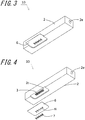
FIG. 3 is a perspective view of the package shown inFIG. 1 , as viewed obliquely from below; -
FIG. 4 is an exploded perspective view of the package shown inFIG. 3 ; -
FIG. 5(a) is a plan view showing an example of one side a wiring substrate, andFIG. 5(b) is a plan view showing an example of the other side of the wiring substrate; -
FIG. 6 is a plan view of the package shown inFIG. 1 ; -
FIG. 7 is a bottom view of the package shown inFIG. 1 ; -
FIG. 8 is a sectional view of the package taken along the line A-A ofFIG. 7 ; -
FIG. 9 is an enlarged sectional view of the main components of the package shown inFIG. 8 ; -
FIG. 10 is a sectional view of the package taken along the line B-B ofFIG. 7 ; -
FIG. 11 is an enlarged sectional view of the main components of the package shown inFIG. 10 ; -
FIG. 12 is a chart for explaining high-frequency characteristics; and -
FIG. 13 is a plan view showing an LN modulator according to one embodiment of the invention. - Referring now to the drawings, an embodiment of the invention will be described below.
- For convenience in illustrating the invention, of the constituent components of one embodiment of the invention, only the main components which are necessary for the understanding of the invention are shown in simplified form in each drawing to be hereafter referred to. Thus, on an as-needed basis, a functional element housing package, an LN modulator, or a semiconductor device according to the invention may be provided with additional members which are not shown in each drawing to be hereafter referred to. Moreover, in each drawing, the actual dimensions of each constituent member and dimensional ratio between the members are not represented precisely.
- The following mainly describes an LN modulator mounting an LN optical device by way of example. Note that, with suitable changes in configuration design, for example, a semiconductor device mounting a light-emitting element such as LD or PD or a light-receiving element falls in the range of application of the invention.
-
FIG. 1 is a perspective view showing a functionalelement housing package 10 according to one embodiment of the invention.FIG. 2 is a perspective view of thepackage 10 shown inFIG. 1 , as viewed from the left.FIG. 3 is a perspective view of thepackage 10 shown inFIG. 1 , as viewed obliquely from below.FIG. 4 is an exploded perspective view of thepackage 10 shown inFIG. 3 , with awiring substrate 6 removed.FIG. 5(a) is a plan view of onesurface 6a of thewiring substrate 6, andFIG. 5(b) is a plan view of theother surface 6b of thewiring substrate 6. Moreover,FIG. 6 is a plan view of thepackage 10, as viewed from the top, andFIG. 7 is a plan view of thepackage 10, as viewed from the bottom.FIG. 8 is a sectional view taken along the line A-A ofFIG. 7 , and,FIG. 10 is a sectional view taken along the line B-B ofFIG. 7 .FIG. 9 is an enlarged sectional view of the main components of the package shown inFIG. 8 , and,FIG. 11 is an enlarged sectional view of the main components of the package shown inFIG. 10 . For example, as shown inFIGS. 2 to 4 , the functionalelement housing package 10 according to the present embodiment (hereafter also referred to simply as "package 10") is built as, although not designated by reference symbol in the drawings, a wiring substrate-equipped functional element housing package. - The
package 10 includes ahousing 2 for mounting afunctional element 1. Thefunctional element 1 is disposed on abottom plate portion 2a of thehousing 2. For example, thehousing 2 is formed of a ceramic material, a metal material, a glass material, or a highly heat-resistant resin material. Examples of the ceramic material include an aluminum oxide (Al2O3) sintered body, a mullite (3Al2O3·2SiO2) sintered body, silicon carbide (SiC) sintered body, an aluminum nitride (AlN) sintered body, a silicon nitride (Si3N4), sintered body and glass ceramics. Examples of the metal material include a Fe-based alloy, oxygen-free copper, and SUS. Examples of the glass material include borosilicate glass and quartz glass. Examples of the highly heat-resistant resin material include polyimide. - For example, the
housing 2 has the general form of a rectangular prism which is 30 mm to 100 mm in length, 5 mm to 20 mm in width, and 5 mm to 20 mm in height. Thehousing 2 of this embodiment is, as exemplified, 50 mm in length, 10 mm in width, and 6.5 mm in height. - The
housing 2 is provided with a recessed portion which opens on an upper surface (to which is joined a lid body which will hereafter be described) thereof. That is, thehousing 2 includes aframe portion 2b disposed along the periphery of thebottom plate portion 2a so as to surround the mounting region for thefunctional element 1. Thehousing 2 is composed of thebottom plate portion 2a and theframe portion 2b combined in one piece. Thehousing 2 is produced by joining the separately preparedbottom plate portion 2a andframe portion 2b together via a joining member such as a solder, a brazing material or an adhesive. - The
housing 2 is provided with ahole 2c formed through its outer region. In the package according to this embodiment, thethrough hole 2c is provided in thebottom plate portion 2a of thehousing 2. When the throughhole 2c is provided in thebottom plate portion 2a of thehousing 2, it is possible to reduce the area required to place thehousing 2 on an external wiring board on which thehousing 2 is mounted. Note that the throughhole 2c may be provided in theframe portion 2b as needed. - A
pin terminal 3 is located in the throughhole 2c of thehousing 2. Thepin terminal 3 is passed through (inserted into) the throughhole 2c in its lengthwise direction and fixed in place. Thepin terminal 3 allows a high-frequency electric signal to be conducted between the interior of thehousing 2 and the exterior thereof. Thepin terminal 3 is disposed in the throughhole 2c, with a dielectric 3a lying between thepin terminal 3 and the surface of the inner periphery of the throughhole 2c. Thepin terminal 3 and the throughhole 2c define a coaxial line structure suited to conducting high-frequency electric signals. - The
pin terminal 3 is formed of metal such as a Fe-Ni material or a Fe-Ni-Co material in linear form which is 0.2 mm to 1 mm in thickness and 2 mm to 5 mm in length. Moreover, thedielectric body 3a is formed of a dielectric material such as ceramics, glass, or resin. Thedielectric body 3a provides a seal between thepin terminal 3 and the surface of the inner periphery of the throughhole 2c. The dielectric 3a serves also as a bonding material for adhering thepin terminal 3 to the inner side of the throughhole 2c. Thepin terminal 3 is not limited in number to one. For example, in thepackage 10 according to this embodiment, a plurality ofpin terminals 3 are aligned in parallel with the side wall of theframe portion 2b. Moreover, as practiced in this embodiment, thepin terminal 3 may be implemented by setting a plurality ofpin terminals 3 anddielectric bodies 3a inside atubular body 3b, and thereafter joining thistubular body 3b to thehousing 2. - In this embodiment, by way of example, the
pin terminal 3 is formed of metal which is 0.3 mm in thickness and 3.45 mm in length. As thedielectric body 3a, a low-melting-point glass material is placed so as to fill the gap between thepin terminal 3 and the inner wall surface of the throughhole 2c which is 1.6 mm in inside diameter. - Moreover, for example, the outer region of the
housing 2 is provided with, in addition to thepin terminal 3, an input-output terminal for providing electrical conduction between the interior of thehousing 2 and the exterior thereof and inputting a direct current. For example, the input-output terminal is disposed in theframe portion 2b, and used for the conduction of low-frequency signals, for example, for the supply of bias potential. The input-output terminal comprises conductor wiring passed through the interior of an insulating material. In this construction, the conductor wiring located inside theframe portion 2b is electrically connected to an internally-provided electronic element, etc. via a wire (bonding wire), for example. The conductor wiring located outside of theframe portion 2b is connected with a lead terminal, etc. - Meanwhile, the
wiring substrate 6 is connected exteriorly to thepin terminal 3. For example, thewiring substrate 6 is an FPC (Flexible Printed Circuit) substrate. The FPC substrate is a flexible substrate composed of a base film formed of a resin film such as a polyimide film, with connection wiring located thereon. That is, the FPC substrate is foldable and bendable. Note that thewiring substrate 6 is not limited to the FPC substrate, but may be a non-flexible substrate such as a glass-epoxy substrate, for example. -
FIG. 5 is a plan view showing both sides of thewiring substrate 6 by way of example.FIG. 5(a) shows onesurface 6a (front side) of thewiring substrate 6, andFIG. 5(b) shows theother surface 6b (back side) of thewiring substrate 6 opposed to the onesurface 6a. Although four through holes H are depicted inFIG. 5 , the invention is not limited to this. That is, the number of the through holes H and associated conductors is equal to the number of thepin terminals 3 and is arbitrary. - The one
surface 6a of thewiring substrate 6 is provided with a firstmetallic layer 6c located around the opening of the through hole H so as to surround the opening the through hole H. Around the firstmetallic layer 6c, there is provided agrounding conductor layer 6f in spaced relation thereto. Thegrounding conductor layer 6f has the form of so-called solid metallic layer. Moreover, theother surface 6b of thewiring substrate 6 is provided with a secondmetallic layer 6d located around the opening of the through hole H so as to surround the opening of the through hole H. The secondmetallic layer 6d is connected with aconnection wiring line 6e extending to an end of the wiring substrate 6 (extending outwardly of the housing 2). - Moreover, in this embodiment, by way of example, a
grounding pad 6g for permitting connection with the grounding conductor layer is provided around the secondmetallic layer 6d. Thegrounding pad 6g is located around the opening of a through hole HE. On the back side of thegrounding pad 6g (onesurface 6a), thegrounding conductor layer 6f is formed around the through hole HE. - Where the
wiring substrate 6 is built as an FPC substrate, the other end of the FPC substrate (substrate 6's end) is connected to an external circuit board (not shown). On the external circuit board, there are provided an electrode pad which is capable of connecting the other end of theconnection wiring line 6e to the wiring of the external wiring board, and a connector, etc., for example. - For example, an insulating layer is provided to cover the
wiring substrate 6, except its conductor end portions for establishing electrical connection with thepin terminal 3, agrounding pin terminal 4, and the external wiring board, or equivalently, the firstmetallic layer 6c, the secondmetallic layer 6d, theconnection wiring line 6e, and the electrically connectable distal end of thegrounding conductor layer 6f. InFIGS. 5(a) and 5(b) , there are shown the individual internal conductors of thewiring substrate 6, with the insulating layer omitted. - The second
metallic layer 6d is greater in area than the firstmetallic layer 6c. For example, the secondmetallic layer 6d in circular form is 0.6 mm in diameter, whereas the firstmetallic layer 6c in circular form is 0.5 mm in diameter. Moreover, the firstmetallic layer 6c and the secondmetallic layer 6d are of symmetrical configuration about the center axis of the through hole H. - Around the second
metallic layer 6d and theconnection wiring line 6e, for example, a grounding conductor layer is formed at a predetermined interval. With the formation of the grounding conductor layer, theconnection wiring line 6e serves, in conjunction with the grounding conductor layer, as a coplanar waveguide. This allows thewiring substrate 6 to effect transmission of high-frequency electric signals. Moreover, when thegrounding conductor layer 6f is formed on the onesurface 6a, the wiring substrate can be caused to function as so-called grounded coplanar waveguide. - Moreover, for example, the
wiring substrate 6 can be caused to function as a microstrip waveguide where theother surface 6b remains free of the grounding conductor layer. In thewiring substrate 6 of this embodiment, a case where a microstrip waveguide is formed is exemplified. That is, thegrounding conductor layer 6f is formed on the back side (onesurface 6a) of theconnection wiring line 6e situated on theother surface 6b. Theconnection wiring line 6e and thegrounding conductor layer 6f constitute the microstrip waveguide. - The
connection wiring line 6e does not necessarily have to be located on theother surface 6b. For example, theconnection wiring line 6e may be located on the onesurface 6a so as to be connected to the firstmetallic layer 6c. In this case, in order to cause them to function as a microstrip waveguide, thegrounding conductor layer 6f is disposed on theother surface 6b which is opposed to theconnection wiring line 6e. - The
wiring substrate 6 so constructed is placed outside of thehousing 2, with the onesurface 6a facing toward thehousing 2, and with the front end of thepin terminal 3 received in the through hole H. Then, thepin terminal 3 is connected to the firstmetallic layer 6c and the secondmetallic layer 6d via a solder 7 (solder 7a andsolder 7b), whereupon thewiring substrate 6 is secured to thehousing 2. As thesolder 7, heretofore knownsolder 7 such as Sn-Ag-Cu solder, Sn-Zn-Bi solder, or Sn-Cu solder, for example, is used. Thesolder 7b is applied as a continuous solder portion extending from the secondmetallic layer 6d, through the outer periphery of thepin terminal 3, to the front end of thepin terminal 3. This allows thewiring substrate 6 to be secured to thetubular body 3b firmly. When thegrounding conductor layer 6f is present, thegrounding conductor layer 6f and thehousing 2 are concurrently connected to each other viasolder 7c, as will hereafter be described in detail. - In this embodiment, the
grounding pin terminal 4 is also concurrently connected to thegrounding pad 6g and thegrounding conductor layer 6f via another solder (solder 7c andsolder 7d). For example, thegrounding pin terminal 4 protruding from the metal-madetubular body 3b is inserted into the through hole HE, and fixedly joined to thegrounding conductor layer 6f and thegrounding pad 6g via thesolder 7c and thesolder 7d. Moreover, thesolder 7c and thesolder 7d are applied as a continuous solder portion extending from the surface of thetubular body 3b to the front end of thegrounding pin terminal 4. This makes it possible to secure thewiring substrate 6 to thetubular body 3b firmly, as well as to minimize the likelihood that an excess of thesolder 7c and thesolder 7d will spread wettably through thetubular body 3b, causing application ofsuperfluous solder 7c to thegrounding pin terminal 4 located between thewiring substrate 6 and thetubular body 3b. Thus, thepackage 10 according to the embodiment of the invention is capable of minimizing the likelihood that the value of characteristic impedance will deviate from the desired value at thepin terminal 3 located between thetubular body 3b and thewiring substrate 6. - Moreover, in this construction, the
pin terminal 3 is configured so that the length of a part thereof which protrudes through theother surface 6b of thewiring substrate 6 is shorter than the length of a part of thegrounding pin terminal 4 which protrudes through theother surface 6b of thewiring substrate 6. This allows thepackage 10 according to the embodiment of the invention to minimize the likelihood that thepin terminal 3 will be brought into contact with human body or an external member in the course of manufacture of thepackage 10, the semiconductor device, and the LN modulator. Thus, a likelihood that thepin terminal 3 will undergo deformation or breaking can be reduced, and occurrence of product defects can be reduced. - Moreover, the
wiring substrate 6 is fixedly joined to thetubular body 3b, with a gap left between thewiring substrate 6 and the upper surface of thetubular body 3b (where thegrounding pin terminal 4 is disposed). Consequently, in thepackage 10 according to the embodiment of the invention, thewiring substrate 6 becomes deformed to the desired extent in the course of manufacture of thepackage 10, the semiconductor device, and the LN modulator. This makes it possible to achieve distribution of the stress exerted on the deformed connection portion of thewiring substrate 6 and thegrounding pin terminal 4, and thereby minimize the likelihood of detachment of thewiring substrate 6 from thegrounding pin terminal 4. - While the surface of the inner periphery of the through hole H is free of a metallic conductor, the
molten solder 7 spreads freely for distribution through the firstmetallic layer 6c and the secondmetallic layer 6d via thepin terminal 3. The distribution of thesolder 7 between the firstmetallic layer 6c and the secondmetallic layer 6d depends on the area ratio between the layers. Consequently, thesolder 7b connecting thepin terminal 3 to the secondmetallic layer 6d of wider area is greater in volume than thesolder 7a connecting thepin terminal 3 to the firstmetallic layer 6c. The volume of thesolder 7b connecting thepin terminal 3 to the secondmetallic layer 6d can be increased. - The
pin terminal 3 and the throughhole 2c (or thetubular body 3b) define a coaxial line structure. A high-frequency signal is transmitted from theconnection wiring line 6e through the secondmetallic layer 6d to thepin terminal 3, and then propagates through the coaxial line defined by thepin terminal 3 and the throughhole 2c (or thetubular body 3b). However, when the firstmetallic layer 6c and thesolder 7a joining the firstmetallic layer 6c to thepin terminal 3 are present at some intermediate part of the coaxial line, uniformity in coaxial structure at this part is lost, and therefore the propagation of high-frequency signal may be disturbed and signal losses may occur. Meanwhile, the joining portion of the secondmetallic layer 6d and thepin terminal 3 is located outside of the coaxial line structure, and the influence on high-frequency signal losses is considered to be small. - Thus, the connection of the
pin terminal 3 is made via the firstmetallic layer 6c and the secondmetallic layer 6d which is greater in area than the firstmetallic layer 6c, and also thesolder 7b is greater in volume than thesolder 7a connecting thepin terminal 3 to the firstmetallic layer 6c. This makes it possible to improve the electrical characteristics of the high-frequency signal line structure, as well as to enhance the strength of connection between thepin terminal 3 and thewiring substrate 6. - For example, a part lying between the
wiring substrate 6 and thehousing 2 of thepin terminal 3 is shorter than a part protruding through theother surface 6b of thewiring substrate 6 of thepin terminal 3. It is preferable that a part lying between thehousing 2 and thewiring substrate 6 of thepin terminal 3 is smaller in surface area than a part protruding from the second metallic layer of thewiring substrate 6 of thepin terminal 3. - Where the part lying between the
housing 2 and thewiring substrate 6 of thepin terminal 3 is smaller in surface area than the part protruding from thewiring substrate 6 of thepin terminal 3, the volume of thesolder 7a provided within the described coaxial line structure can be reduced, whereas the volume of thesolder 7b which is believed to have little influence on high-frequency characteristics can be increased. This makes it possible to maintain the electrical characteristics of the interior of the coaxial line structure satisfactorily, as well as to enhance the joining strength between thepin terminal 3 and thewiring substrate 6 at the front end of thepin terminal 3. - Further, the first
metallic layer 6c and the secondmetallic layer 6d are of a symmetrical shape with respect to thepin terminal 3, for example, a circular shape. Thus, thesolder 7a and thesolder 7b joining thepin terminal 3 to the first and secondmetallic layers pin terminal 3. This allows the coaxial line structure defined by thepin terminal 3 and the throughhole 2c to be symmetrical about the center axis of thepin terminal 3, and thus to maintain the high-frequency electrical characteristics satisfactorily. Moreover, the thermal stress exerted on the connection portion of thepin terminal 3 and thewiring substrate 6 is developed symmetrically around thepin terminal 3. This helps reduce localized stress application to part of thesolder 7a. - The
solder 7b joining thepin terminal 3 to the secondmetallic layer 6d is wider in surface area than thesolder 7a joining thepin terminal 3 to the firstmetallic layer 6c. This makes it possible to increase electrostatic capacitance among a part of thepin terminal 3 protruding out of thewiring substrate 6, thegrounding pin terminal 4, and thegrounding conductor layer 6f provided in thewiring substrate 6. - It has been found that an improvement in high-frequency characteristics can be achieved by so securing the
wiring substrate 6 via thesolder 7.FIG. 12 is a chart indicating a TDR (time domain reflectometry) measurement-based comparison of the high-frequency characteristics of the packages with respect to the dimensions of the firstmetallic layer 6c and the secondmetallic layer 6d. InFIG. 12 , the broken line A represents the result of measurement as to a case where the firstmetallic layer 6c and the secondmetallic layer 6d have the same exterior size set at 0.6 mm. The solid line B represents the result of measurement as to a case where the firstmetallic layer 6c and the secondmetallic layer 6d are 0.5 mm and 0.6 mm, respectively, in exterior size, and thesolder 7a is smaller in volume than thesolder 7b. - It will be understood from
FIG. 12 that, in the case where the firstmetallic layer 6c is smaller in area than the secondmetallic layer 6d or in the case where thesolder 7a is smaller in volume than thesolder 7b, thepackage 10 is advantageous in characteristic impedance matching. That is, in this case, it has been found that a deviation from the characteristic impedance of 50 Ω has been improved from 47 Ω to 49 Ω at the position joined to thepin terminal 3,, which shows 2-Ω improvement has been achieved. - Moreover, the
solder 7b and thesolder 7d are applied so that the spacing between them becomes wider gradually toward the front end of each of thepin terminal 3 and thegrounding pin terminal 4. This allows thepackage 10 according to the embodiment of the invention to minimize the likelihood that characteristic impedance fluctuations will occur at the joining portion of thewiring substrate 6 and thepin terminal 3 as well as thegrounding pin terminal 4. - The functional element housing package (package) 10 according to the present embodiment receives the
functional element 1 inside thehousing 2. Examples of thefunctional element 1 include LN optical devices utilizing an electro-optic crystal such as a lithium niobate substrate, and semiconductor elements such as LD and PD. Each such a semiconductor element is a high-frequency semiconductor element which operates with high-frequency electric signals. In addition, examples of functional elements which operate with high-frequency electric signals include a resistor, a piezoelectric element, a quartz oscillator, and a ceramic oscillator. Note that the high-frequency range assumed for this construction corresponds roughly to the range of 1 GHz to 100 GHz. Referring now toFIG. 13 , anLN modulator 11 using an LN optical device which serves as thefunctional element 1 will be described by way of example. - The
functional element 1 such as an LN optical device is placed on thebottom plate portion 2a of thehousing 2, with an electrode thereof connected to thepin terminal 3. Moreover, thehousing 2 is provided with securingmembers holes Optical fibers hole member member optical fiber housing 2. - A waveguide is formed on the LN optical device. An optical signal inputted through one
optical fiber 8a attached to the securingmember 9a is optically coupled to one end of the waveguide, and propagates over the waveguide. After undergoing modulation on the LN optical device under the action of a high-frequency electric signal fed from thepin terminal 3 through a bonding wire W, the optical signal is outputted from the other end of the waveguide toward the otheroptical fiber 8b attached to the securingmember 9b. - Lastly, a lid body (not shown) is joined to the upper surface of the
frame portion 2b. That is, the lid body is bonded to the upper surface of theframe portion 2b via a connecting member such as a solder or a brazing material so as to define, for example, a sealed hollow structure by closing the functional element 1-housing space formed by thehousing 2 for hermetic sealing. - As described above, according to the invention, the second
metallic layer 6d which is greater in area than the firstmetallic layer 6c and thepin terminal 3 are connected to each other via thesolder 7. Thus, it is possible to provide the functionalelement housing package 10, as well as thesemiconductor device 11 and theLN modulator 11 which have excellent high-frequency characteristics. - It should be understood that the application of the invention is not limited to the described embodiments and examples, and that various changes and modifications are possible without departing from the scope of the invention. For example, although the area per se of the first
metallic layer 6c is adjusted to be smaller than the area of the secondmetallic layer 6d in the described embodiment, the invention is not limited to this. For example, the firstmetallic layer 6c may be made equal to or greater than the secondmetallic layer 6d in area. In this case, the outer periphery of the firstmetallic layer 6c is covered with the insulating layer covering the onesurface 6a of thewiring substrate 6. Consequently, the area of the exposed inner periphery of the firstmetallic layer 6c subjected to application of thesolder 7a is smaller than the area of the exposed secondmetallic layer 6d. This makes it possible to substantially reduce the area of the firstmetallic layer 6c subjected to application of thesolder 7a, and thereby adjust the volume of thesolder 7a connecting thepin terminal 3 to the firstmetallic layer 6c to be smaller than the volume of thesolder 7b connecting thepin terminal 3 to the secondmetallic layer 6d. - Moreover, as employed in the description of the embodiment, the terms "top", "upper", "bottom", "left", right", etc. are used merely for the purpose of explaining the relation between the positions of constituent components as viewed in each drawing, and thus these terms do not represent positional relationship in the construction in actual use.
-
- 1:
- Functional element
- 2:
- Housing
- 2a:
- Bottom plate portion
- 2b:
- Frame portion
- 2c:
- Through hole
- 2d, 2e:
- Optical fiber-mounting hole
- 3:
- Pin terminal
- 3a:
- Dielectric body
- 4:
- Grounding pin terminal
- 6:
- Wiring substrate
- 6a:
- One surface
- 6b:
- Other surface
- 6c:
- First metallic layer
- 6d:
- Second metallic layer
- 6e:
- Connection wiring line
- 6f:
- Grounding conductor layer
- 6g:
- Grounding pad
- 7:
- Solder
- 8a, 8b:
- Optical fiber
- 9a, 9b:
- Securing member
- W:
- Bonding wire
- H:
- Through hole
Claims (7)
- A functional element housing package, comprising:a housing which houses a functional element;a pin terminal disposed in an outer region of the housing; anda wiring substrate comprisinga through hole for receiving the pin terminal,a first metallic layer disposed around an opening of the through hole on a side of the wiring substrate which side is located close to the housing,a second metallic layer disposed around an opening of the through hole on a side of the wiring substrate which side is opposed to the side located close to the housing, the second metallic layer being greater in area than the first metallic layer,a connection wiring line connected to the first metallic layer or the second metallic layer, anda solder which connects the pin terminal to each of the first metallic layer and the second metallic layer.
- The functional element housing package according to claim 1,
wherein a part of the solder connecting the pin terminal to the first metallic layer is smaller in volume than a part of the solder connecting the pin terminal to the second metallic layer. - The functional element housing package according to claim 1 or 2,
wherein a part lying between the housing and the wiring substrate of the pin terminal is smaller in surface area than a part protruding through the second metallic layer of the pin terminal. - The functional element housing package according to any one of claims 1 to 3,
wherein the first metallic layer and the second metallic layer are of symmetrical configuration about a center axis, and
the pin terminal is positioned in the center axis. - The functional element housing package according to any one of claims 1 to 4,
wherein the pin terminal is disposed on a bottom surface of the housing. - A semiconductor device, comprising:the functional element housing package according to any one of claims 1 to 5; anda semiconductor element housed inside the housing.
- An LN modulator, comprising:the functional element housing package according to any one of claims 1 to 5; andan LN optical device housed inside the housing.
Applications Claiming Priority (2)
| Application Number | Priority Date | Filing Date | Title |
|---|---|---|---|
| JP2016061104 | 2016-03-25 | ||
| PCT/JP2017/012386 WO2017164418A1 (en) | 2016-03-25 | 2017-03-27 | Package for storing functional element, semiconductor device and ln modulator |
Publications (3)
| Publication Number | Publication Date |
|---|---|
| EP3428961A1 true EP3428961A1 (en) | 2019-01-16 |
| EP3428961A4 EP3428961A4 (en) | 2019-03-27 |
| EP3428961B1 EP3428961B1 (en) | 2020-05-13 |
Family
ID=59900540
Family Applications (1)
| Application Number | Title | Priority Date | Filing Date |
|---|---|---|---|
| EP17770457.4A Active EP3428961B1 (en) | 2016-03-25 | 2017-03-27 | Package for storing functional element, semiconductor device and ln modulator |
Country Status (4)
| Country | Link |
|---|---|
| US (1) | US11815749B2 (en) |
| EP (1) | EP3428961B1 (en) |
| JP (1) | JP6599548B2 (en) |
| WO (1) | WO2017164418A1 (en) |
Families Citing this family (6)
| Publication number | Priority date | Publication date | Assignee | Title |
|---|---|---|---|---|
| US11070006B2 (en) | 2017-08-03 | 2021-07-20 | Amphenol Corporation | Connector for low loss interconnection system |
| CN115632285A (en) | 2018-04-02 | 2023-01-20 | 安达概念股份有限公司 | Controlled impedance cable connector and device coupled with same |
| CN113557459B (en) | 2019-01-25 | 2023-10-20 | 富加宜(美国)有限责任公司 | I/O connector configured for cable connection to midplane |
| WO2020154507A1 (en) | 2019-01-25 | 2020-07-30 | Fci Usa Llc | I/o connector configured for cable connection to a midboard |
| US11735852B2 (en) | 2019-09-19 | 2023-08-22 | Amphenol Corporation | High speed electronic system with midboard cable connector |
| CN113258325A (en) * | 2020-01-28 | 2021-08-13 | 富加宜(美国)有限责任公司 | High-frequency middle plate connector |
Family Cites Families (4)
| Publication number | Priority date | Publication date | Assignee | Title |
|---|---|---|---|---|
| JP5682182B2 (en) | 2010-08-30 | 2015-03-11 | 富士通オプティカルコンポーネンツ株式会社 | Optical modulator module |
| JP6258724B2 (en) * | 2013-02-27 | 2018-01-10 | 京セラ株式会社 | Electronic component mounting package and electronic device using the same |
| JP5786883B2 (en) * | 2013-03-29 | 2015-09-30 | 住友大阪セメント株式会社 | Optical device |
| JP6281428B2 (en) * | 2014-07-11 | 2018-02-21 | 富士通オプティカルコンポーネンツ株式会社 | Optical module and transmitter |
-
2017
- 2017-03-27 WO PCT/JP2017/012386 patent/WO2017164418A1/en active Application Filing
- 2017-03-27 US US16/087,985 patent/US11815749B2/en active Active
- 2017-03-27 EP EP17770457.4A patent/EP3428961B1/en active Active
- 2017-03-27 JP JP2018507465A patent/JP6599548B2/en active Active
Also Published As
| Publication number | Publication date |
|---|---|
| US11815749B2 (en) | 2023-11-14 |
| JPWO2017164418A1 (en) | 2019-01-31 |
| WO2017164418A1 (en) | 2017-09-28 |
| EP3428961A4 (en) | 2019-03-27 |
| EP3428961B1 (en) | 2020-05-13 |
| US20210208428A1 (en) | 2021-07-08 |
| JP6599548B2 (en) | 2019-10-30 |
Similar Documents
| Publication | Publication Date | Title |
|---|---|---|
| EP3428961B1 (en) | Package for storing functional element, semiconductor device and ln modulator | |
| US6876004B2 (en) | Circuit interconnect for optoelectronic device for controlled impedance at high frequencies | |
| KR20120054209A (en) | Optical modules | |
| JP2009302438A (en) | Optical semiconductor device | |
| JP7063695B2 (en) | Optical module | |
| JP7249745B2 (en) | Optical subassemblies and optical modules | |
| US11703378B2 (en) | Optical module | |
| CN112305683A (en) | Optical module | |
| JP5241562B2 (en) | Connection device, package for storing semiconductor element with flexible substrate, and semiconductor device with flexible substrate | |
| US9386687B2 (en) | Electronic component housing package and electronic apparatus | |
| JP2022132918A (en) | optical module | |
| WO2020175626A1 (en) | Electronic-element mounting package and electronic device | |
| JP2019186379A (en) | Optical module | |
| JP2009283898A (en) | Electronic part container, package for storing electronic part using the same and electronic device | |
| JP7036646B2 (en) | Packages for semiconductor devices and semiconductor devices | |
| JPS62124780A (en) | Optical semiconductor module | |
| JP4041226B2 (en) | Optical semiconductor device | |
| JP6671567B1 (en) | Optical module | |
| JP2000164970A (en) | Optical element module | |
| CA2305954A1 (en) | Package for high-frequency device | |
| JP2004200279A (en) | Photoelectric device | |
| JP4231166B2 (en) | Optical semiconductor device | |
| JPH11339898A (en) | High frequency input and output terminal, and package for high frequency circuit | |
| JP2019041045A (en) | Package for electronic component housing and electronic device | |
| JPH11186456A (en) | Mmic module |
Legal Events
| Date | Code | Title | Description |
|---|---|---|---|
| STAA | Information on the status of an ep patent application or granted ep patent |
Free format text: STATUS: THE INTERNATIONAL PUBLICATION HAS BEEN MADE |
|
| PUAI | Public reference made under article 153(3) epc to a published international application that has entered the european phase |
Free format text: ORIGINAL CODE: 0009012 |
|
| STAA | Information on the status of an ep patent application or granted ep patent |
Free format text: STATUS: REQUEST FOR EXAMINATION WAS MADE |
|
| 17P | Request for examination filed |
Effective date: 20181011 |
|
| AK | Designated contracting states |
Kind code of ref document: A1 Designated state(s): AL AT BE BG CH CY CZ DE DK EE ES FI FR GB GR HR HU IE IS IT LI LT LU LV MC MK MT NL NO PL PT RO RS SE SI SK SM TR |
|
| AX | Request for extension of the european patent |
Extension state: BA ME |
|
| A4 | Supplementary search report drawn up and despatched |
Effective date: 20190225 |
|
| RIC1 | Information provided on ipc code assigned before grant |
Ipc: H01L 23/02 20060101AFI20190219BHEP Ipc: G02F 1/03 20060101ALI20190219BHEP |
|
| STAA | Information on the status of an ep patent application or granted ep patent |
Free format text: STATUS: EXAMINATION IS IN PROGRESS |
|
| DAV | Request for validation of the european patent (deleted) | ||
| DAX | Request for extension of the european patent (deleted) | ||
| 17Q | First examination report despatched |
Effective date: 20190624 |
|
| GRAP | Despatch of communication of intention to grant a patent |
Free format text: ORIGINAL CODE: EPIDOSNIGR1 |
|
| STAA | Information on the status of an ep patent application or granted ep patent |
Free format text: STATUS: GRANT OF PATENT IS INTENDED |
|
| INTG | Intention to grant announced |
Effective date: 20191212 |
|
| GRAS | Grant fee paid |
Free format text: ORIGINAL CODE: EPIDOSNIGR3 |
|
| GRAA | (expected) grant |
Free format text: ORIGINAL CODE: 0009210 |
|
| STAA | Information on the status of an ep patent application or granted ep patent |
Free format text: STATUS: THE PATENT HAS BEEN GRANTED |
|
| AK | Designated contracting states |
Kind code of ref document: B1 Designated state(s): AL AT BE BG CH CY CZ DE DK EE ES FI FR GB GR HR HU IE IS IT LI LT LU LV MC MK MT NL NO PL PT RO RS SE SI SK SM TR |
|
| REG | Reference to a national code |
Ref country code: GB Ref legal event code: FG4D |
|
| REG | Reference to a national code |
Ref country code: CH Ref legal event code: EP |
|
| REG | Reference to a national code |
Ref country code: DE Ref legal event code: R096 Ref document number: 602017016761 Country of ref document: DE |
|
| REG | Reference to a national code |
Ref country code: AT Ref legal event code: REF Ref document number: 1271345 Country of ref document: AT Kind code of ref document: T Effective date: 20200615 |
|
| REG | Reference to a national code |
Ref country code: LT Ref legal event code: MG4D |
|
| REG | Reference to a national code |
Ref country code: NL Ref legal event code: MP Effective date: 20200513 |
|
| PG25 | Lapsed in a contracting state [announced via postgrant information from national office to epo] |
Ref country code: GR Free format text: LAPSE BECAUSE OF FAILURE TO SUBMIT A TRANSLATION OF THE DESCRIPTION OR TO PAY THE FEE WITHIN THE PRESCRIBED TIME-LIMIT Effective date: 20200814 Ref country code: FI Free format text: LAPSE BECAUSE OF FAILURE TO SUBMIT A TRANSLATION OF THE DESCRIPTION OR TO PAY THE FEE WITHIN THE PRESCRIBED TIME-LIMIT Effective date: 20200513 Ref country code: PT Free format text: LAPSE BECAUSE OF FAILURE TO SUBMIT A TRANSLATION OF THE DESCRIPTION OR TO PAY THE FEE WITHIN THE PRESCRIBED TIME-LIMIT Effective date: 20200914 Ref country code: LT Free format text: LAPSE BECAUSE OF FAILURE TO SUBMIT A TRANSLATION OF THE DESCRIPTION OR TO PAY THE FEE WITHIN THE PRESCRIBED TIME-LIMIT Effective date: 20200513 Ref country code: NO Free format text: LAPSE BECAUSE OF FAILURE TO SUBMIT A TRANSLATION OF THE DESCRIPTION OR TO PAY THE FEE WITHIN THE PRESCRIBED TIME-LIMIT Effective date: 20200813 Ref country code: SE Free format text: LAPSE BECAUSE OF FAILURE TO SUBMIT A TRANSLATION OF THE DESCRIPTION OR TO PAY THE FEE WITHIN THE PRESCRIBED TIME-LIMIT Effective date: 20200513 Ref country code: IS Free format text: LAPSE BECAUSE OF FAILURE TO SUBMIT A TRANSLATION OF THE DESCRIPTION OR TO PAY THE FEE WITHIN THE PRESCRIBED TIME-LIMIT Effective date: 20200913 |
|
| PG25 | Lapsed in a contracting state [announced via postgrant information from national office to epo] |
Ref country code: BG Free format text: LAPSE BECAUSE OF FAILURE TO SUBMIT A TRANSLATION OF THE DESCRIPTION OR TO PAY THE FEE WITHIN THE PRESCRIBED TIME-LIMIT Effective date: 20200813 Ref country code: RS Free format text: LAPSE BECAUSE OF FAILURE TO SUBMIT A TRANSLATION OF THE DESCRIPTION OR TO PAY THE FEE WITHIN THE PRESCRIBED TIME-LIMIT Effective date: 20200513 Ref country code: HR Free format text: LAPSE BECAUSE OF FAILURE TO SUBMIT A TRANSLATION OF THE DESCRIPTION OR TO PAY THE FEE WITHIN THE PRESCRIBED TIME-LIMIT Effective date: 20200513 Ref country code: LV Free format text: LAPSE BECAUSE OF FAILURE TO SUBMIT A TRANSLATION OF THE DESCRIPTION OR TO PAY THE FEE WITHIN THE PRESCRIBED TIME-LIMIT Effective date: 20200513 |
|
| REG | Reference to a national code |
Ref country code: AT Ref legal event code: MK05 Ref document number: 1271345 Country of ref document: AT Kind code of ref document: T Effective date: 20200513 |
|
| PG25 | Lapsed in a contracting state [announced via postgrant information from national office to epo] |
Ref country code: AL Free format text: LAPSE BECAUSE OF FAILURE TO SUBMIT A TRANSLATION OF THE DESCRIPTION OR TO PAY THE FEE WITHIN THE PRESCRIBED TIME-LIMIT Effective date: 20200513 Ref country code: NL Free format text: LAPSE BECAUSE OF FAILURE TO SUBMIT A TRANSLATION OF THE DESCRIPTION OR TO PAY THE FEE WITHIN THE PRESCRIBED TIME-LIMIT Effective date: 20200513 |
|
| PG25 | Lapsed in a contracting state [announced via postgrant information from national office to epo] |
Ref country code: ES Free format text: LAPSE BECAUSE OF FAILURE TO SUBMIT A TRANSLATION OF THE DESCRIPTION OR TO PAY THE FEE WITHIN THE PRESCRIBED TIME-LIMIT Effective date: 20200513 Ref country code: DK Free format text: LAPSE BECAUSE OF FAILURE TO SUBMIT A TRANSLATION OF THE DESCRIPTION OR TO PAY THE FEE WITHIN THE PRESCRIBED TIME-LIMIT Effective date: 20200513 Ref country code: AT Free format text: LAPSE BECAUSE OF FAILURE TO SUBMIT A TRANSLATION OF THE DESCRIPTION OR TO PAY THE FEE WITHIN THE PRESCRIBED TIME-LIMIT Effective date: 20200513 Ref country code: EE Free format text: LAPSE BECAUSE OF FAILURE TO SUBMIT A TRANSLATION OF THE DESCRIPTION OR TO PAY THE FEE WITHIN THE PRESCRIBED TIME-LIMIT Effective date: 20200513 Ref country code: RO Free format text: LAPSE BECAUSE OF FAILURE TO SUBMIT A TRANSLATION OF THE DESCRIPTION OR TO PAY THE FEE WITHIN THE PRESCRIBED TIME-LIMIT Effective date: 20200513 Ref country code: CZ Free format text: LAPSE BECAUSE OF FAILURE TO SUBMIT A TRANSLATION OF THE DESCRIPTION OR TO PAY THE FEE WITHIN THE PRESCRIBED TIME-LIMIT Effective date: 20200513 Ref country code: IT Free format text: LAPSE BECAUSE OF FAILURE TO SUBMIT A TRANSLATION OF THE DESCRIPTION OR TO PAY THE FEE WITHIN THE PRESCRIBED TIME-LIMIT Effective date: 20200513 Ref country code: SM Free format text: LAPSE BECAUSE OF FAILURE TO SUBMIT A TRANSLATION OF THE DESCRIPTION OR TO PAY THE FEE WITHIN THE PRESCRIBED TIME-LIMIT Effective date: 20200513 |
|
| REG | Reference to a national code |
Ref country code: DE Ref legal event code: R097 Ref document number: 602017016761 Country of ref document: DE |
|
| PG25 | Lapsed in a contracting state [announced via postgrant information from national office to epo] |
Ref country code: SK Free format text: LAPSE BECAUSE OF FAILURE TO SUBMIT A TRANSLATION OF THE DESCRIPTION OR TO PAY THE FEE WITHIN THE PRESCRIBED TIME-LIMIT Effective date: 20200513 Ref country code: PL Free format text: LAPSE BECAUSE OF FAILURE TO SUBMIT A TRANSLATION OF THE DESCRIPTION OR TO PAY THE FEE WITHIN THE PRESCRIBED TIME-LIMIT Effective date: 20200513 |
|
| PLBE | No opposition filed within time limit |
Free format text: ORIGINAL CODE: 0009261 |
|
| STAA | Information on the status of an ep patent application or granted ep patent |
Free format text: STATUS: NO OPPOSITION FILED WITHIN TIME LIMIT |
|
| 26N | No opposition filed |
Effective date: 20210216 |
|
| PG25 | Lapsed in a contracting state [announced via postgrant information from national office to epo] |
Ref country code: SI Free format text: LAPSE BECAUSE OF FAILURE TO SUBMIT A TRANSLATION OF THE DESCRIPTION OR TO PAY THE FEE WITHIN THE PRESCRIBED TIME-LIMIT Effective date: 20200513 |
|
| REG | Reference to a national code |
Ref country code: DE Ref legal event code: R119 Ref document number: 602017016761 Country of ref document: DE |
|
| PG25 | Lapsed in a contracting state [announced via postgrant information from national office to epo] |
Ref country code: MC Free format text: LAPSE BECAUSE OF FAILURE TO SUBMIT A TRANSLATION OF THE DESCRIPTION OR TO PAY THE FEE WITHIN THE PRESCRIBED TIME-LIMIT Effective date: 20200513 |
|
| REG | Reference to a national code |
Ref country code: CH Ref legal event code: PL |
|
| REG | Reference to a national code |
Ref country code: BE Ref legal event code: MM Effective date: 20210331 |
|
| PG25 | Lapsed in a contracting state [announced via postgrant information from national office to epo] |
Ref country code: LU Free format text: LAPSE BECAUSE OF NON-PAYMENT OF DUE FEES Effective date: 20210327 Ref country code: LI Free format text: LAPSE BECAUSE OF NON-PAYMENT OF DUE FEES Effective date: 20210331 Ref country code: DE Free format text: LAPSE BECAUSE OF NON-PAYMENT OF DUE FEES Effective date: 20211001 Ref country code: CH Free format text: LAPSE BECAUSE OF NON-PAYMENT OF DUE FEES Effective date: 20210331 Ref country code: FR Free format text: LAPSE BECAUSE OF NON-PAYMENT OF DUE FEES Effective date: 20210331 Ref country code: IE Free format text: LAPSE BECAUSE OF NON-PAYMENT OF DUE FEES Effective date: 20210327 |
|
| PGFP | Annual fee paid to national office [announced via postgrant information from national office to epo] |
Ref country code: GB Payment date: 20220203 Year of fee payment: 6 |
|
| PG25 | Lapsed in a contracting state [announced via postgrant information from national office to epo] |
Ref country code: BE Free format text: LAPSE BECAUSE OF NON-PAYMENT OF DUE FEES Effective date: 20210331 |
|
| PG25 | Lapsed in a contracting state [announced via postgrant information from national office to epo] |
Ref country code: CY Free format text: LAPSE BECAUSE OF FAILURE TO SUBMIT A TRANSLATION OF THE DESCRIPTION OR TO PAY THE FEE WITHIN THE PRESCRIBED TIME-LIMIT Effective date: 20200513 |
|
| PG25 | Lapsed in a contracting state [announced via postgrant information from national office to epo] |
Ref country code: HU Free format text: LAPSE BECAUSE OF FAILURE TO SUBMIT A TRANSLATION OF THE DESCRIPTION OR TO PAY THE FEE WITHIN THE PRESCRIBED TIME-LIMIT; INVALID AB INITIO Effective date: 20170327 |
|
| GBPC | Gb: european patent ceased through non-payment of renewal fee |
Effective date: 20230327 |
|
| PG25 | Lapsed in a contracting state [announced via postgrant information from national office to epo] |
Ref country code: GB Free format text: LAPSE BECAUSE OF NON-PAYMENT OF DUE FEES Effective date: 20230327 |
|
| PG25 | Lapsed in a contracting state [announced via postgrant information from national office to epo] |
Ref country code: GB Free format text: LAPSE BECAUSE OF NON-PAYMENT OF DUE FEES Effective date: 20230327 |
|
| PG25 | Lapsed in a contracting state [announced via postgrant information from national office to epo] |
Ref country code: MK Free format text: LAPSE BECAUSE OF FAILURE TO SUBMIT A TRANSLATION OF THE DESCRIPTION OR TO PAY THE FEE WITHIN THE PRESCRIBED TIME-LIMIT Effective date: 20200513 |