EP3422397A1 - Secondary packaging method for through-silicon via chip and secondary package thereof - Google Patents
Secondary packaging method for through-silicon via chip and secondary package thereof Download PDFInfo
- Publication number
- EP3422397A1 EP3422397A1 EP17896308.8A EP17896308A EP3422397A1 EP 3422397 A1 EP3422397 A1 EP 3422397A1 EP 17896308 A EP17896308 A EP 17896308A EP 3422397 A1 EP3422397 A1 EP 3422397A1
- Authority
- EP
- European Patent Office
- Prior art keywords
- solder ball
- tsv chip
- molding compound
- tsv
- secondary package
- Prior art date
- Legal status (The legal status is an assumption and is not a legal conclusion. Google has not performed a legal analysis and makes no representation as to the accuracy of the status listed.)
- Ceased
Links
Images






Classifications
-
- H—ELECTRICITY
- H10—SEMICONDUCTOR DEVICES; ELECTRIC SOLID-STATE DEVICES NOT OTHERWISE PROVIDED FOR
- H10P—GENERIC PROCESSES OR APPARATUS FOR THE MANUFACTURE OR TREATMENT OF DEVICES COVERED BY CLASS H10
- H10P72/00—Handling or holding of wafers, substrates or devices during manufacture or treatment thereof
- H10P72/70—Handling or holding of wafers, substrates or devices during manufacture or treatment thereof for supporting or gripping
- H10P72/74—Handling or holding of wafers, substrates or devices during manufacture or treatment thereof for supporting or gripping using temporarily an auxiliary support
-
- G—PHYSICS
- G06—COMPUTING OR CALCULATING; COUNTING
- G06V—IMAGE OR VIDEO RECOGNITION OR UNDERSTANDING
- G06V40/00—Recognition of biometric, human-related or animal-related patterns in image or video data
- G06V40/10—Human or animal bodies, e.g. vehicle occupants or pedestrians; Body parts, e.g. hands
- G06V40/12—Fingerprints or palmprints
- G06V40/13—Sensors therefor
- G06V40/1329—Protecting the fingerprint sensor against damage caused by the finger
-
- H—ELECTRICITY
- H10—SEMICONDUCTOR DEVICES; ELECTRIC SOLID-STATE DEVICES NOT OTHERWISE PROVIDED FOR
- H10F—INORGANIC SEMICONDUCTOR DEVICES SENSITIVE TO INFRARED RADIATION, LIGHT, ELECTROMAGNETIC RADIATION OF SHORTER WAVELENGTH OR CORPUSCULAR RADIATION
- H10F39/00—Integrated devices, or assemblies of multiple devices, comprising at least one element covered by group H10F30/00, e.g. radiation detectors comprising photodiode arrays
- H10F39/011—Manufacture or treatment of image sensors covered by group H10F39/12
- H10F39/024—Manufacture or treatment of image sensors covered by group H10F39/12 of coatings or optical elements
-
- H—ELECTRICITY
- H10—SEMICONDUCTOR DEVICES; ELECTRIC SOLID-STATE DEVICES NOT OTHERWISE PROVIDED FOR
- H10F—INORGANIC SEMICONDUCTOR DEVICES SENSITIVE TO INFRARED RADIATION, LIGHT, ELECTROMAGNETIC RADIATION OF SHORTER WAVELENGTH OR CORPUSCULAR RADIATION
- H10F39/00—Integrated devices, or assemblies of multiple devices, comprising at least one element covered by group H10F30/00, e.g. radiation detectors comprising photodiode arrays
- H10F39/011—Manufacture or treatment of image sensors covered by group H10F39/12
- H10F39/028—Manufacture or treatment of image sensors covered by group H10F39/12 performed after manufacture of the image sensors, e.g. annealing, gettering of impurities, short-circuit elimination or recrystallisation
-
- H—ELECTRICITY
- H10—SEMICONDUCTOR DEVICES; ELECTRIC SOLID-STATE DEVICES NOT OTHERWISE PROVIDED FOR
- H10F—INORGANIC SEMICONDUCTOR DEVICES SENSITIVE TO INFRARED RADIATION, LIGHT, ELECTROMAGNETIC RADIATION OF SHORTER WAVELENGTH OR CORPUSCULAR RADIATION
- H10F39/00—Integrated devices, or assemblies of multiple devices, comprising at least one element covered by group H10F30/00, e.g. radiation detectors comprising photodiode arrays
- H10F39/80—Constructional details of image sensors
- H10F39/804—Containers or encapsulations
-
- H—ELECTRICITY
- H10—SEMICONDUCTOR DEVICES; ELECTRIC SOLID-STATE DEVICES NOT OTHERWISE PROVIDED FOR
- H10F—INORGANIC SEMICONDUCTOR DEVICES SENSITIVE TO INFRARED RADIATION, LIGHT, ELECTROMAGNETIC RADIATION OF SHORTER WAVELENGTH OR CORPUSCULAR RADIATION
- H10F39/00—Integrated devices, or assemblies of multiple devices, comprising at least one element covered by group H10F30/00, e.g. radiation detectors comprising photodiode arrays
- H10F39/80—Constructional details of image sensors
- H10F39/806—Optical elements or arrangements associated with the image sensors
-
- H—ELECTRICITY
- H10—SEMICONDUCTOR DEVICES; ELECTRIC SOLID-STATE DEVICES NOT OTHERWISE PROVIDED FOR
- H10F—INORGANIC SEMICONDUCTOR DEVICES SENSITIVE TO INFRARED RADIATION, LIGHT, ELECTROMAGNETIC RADIATION OF SHORTER WAVELENGTH OR CORPUSCULAR RADIATION
- H10F39/00—Integrated devices, or assemblies of multiple devices, comprising at least one element covered by group H10F30/00, e.g. radiation detectors comprising photodiode arrays
- H10F39/80—Constructional details of image sensors
- H10F39/811—Interconnections
-
- H—ELECTRICITY
- H10—SEMICONDUCTOR DEVICES; ELECTRIC SOLID-STATE DEVICES NOT OTHERWISE PROVIDED FOR
- H10W—GENERIC PACKAGES, INTERCONNECTIONS, CONNECTORS OR OTHER CONSTRUCTIONAL DETAILS OF DEVICES COVERED BY CLASS H10
- H10W20/00—Interconnections in chips, wafers or substrates
- H10W20/01—Manufacture or treatment
- H10W20/021—Manufacture or treatment of interconnections within wafers or substrates
- H10W20/023—Manufacture or treatment of interconnections within wafers or substrates the interconnections being through-semiconductor vias
-
- H—ELECTRICITY
- H10—SEMICONDUCTOR DEVICES; ELECTRIC SOLID-STATE DEVICES NOT OTHERWISE PROVIDED FOR
- H10W—GENERIC PACKAGES, INTERCONNECTIONS, CONNECTORS OR OTHER CONSTRUCTIONAL DETAILS OF DEVICES COVERED BY CLASS H10
- H10W70/00—Package substrates; Interposers; Redistribution layers [RDL]
- H10W70/60—Insulating or insulated package substrates; Interposers; Redistribution layers
- H10W70/62—Insulating or insulated package substrates; Interposers; Redistribution layers characterised by their interconnections
- H10W70/63—Vias, e.g. via plugs
- H10W70/635—Through-vias
-
- H—ELECTRICITY
- H10—SEMICONDUCTOR DEVICES; ELECTRIC SOLID-STATE DEVICES NOT OTHERWISE PROVIDED FOR
- H10W—GENERIC PACKAGES, INTERCONNECTIONS, CONNECTORS OR OTHER CONSTRUCTIONAL DETAILS OF DEVICES COVERED BY CLASS H10
- H10W72/00—Interconnections or connectors in packages
- H10W72/01—Manufacture or treatment
- H10W72/0198—Manufacture or treatment batch processes
-
- H—ELECTRICITY
- H10—SEMICONDUCTOR DEVICES; ELECTRIC SOLID-STATE DEVICES NOT OTHERWISE PROVIDED FOR
- H10W—GENERIC PACKAGES, INTERCONNECTIONS, CONNECTORS OR OTHER CONSTRUCTIONAL DETAILS OF DEVICES COVERED BY CLASS H10
- H10W72/00—Interconnections or connectors in packages
- H10W72/30—Die-attach connectors
-
- H—ELECTRICITY
- H10—SEMICONDUCTOR DEVICES; ELECTRIC SOLID-STATE DEVICES NOT OTHERWISE PROVIDED FOR
- H10W—GENERIC PACKAGES, INTERCONNECTIONS, CONNECTORS OR OTHER CONSTRUCTIONAL DETAILS OF DEVICES COVERED BY CLASS H10
- H10W74/00—Encapsulations, e.g. protective coatings
- H10W74/01—Manufacture or treatment
-
- H—ELECTRICITY
- H10—SEMICONDUCTOR DEVICES; ELECTRIC SOLID-STATE DEVICES NOT OTHERWISE PROVIDED FOR
- H10W—GENERIC PACKAGES, INTERCONNECTIONS, CONNECTORS OR OTHER CONSTRUCTIONAL DETAILS OF DEVICES COVERED BY CLASS H10
- H10W74/00—Encapsulations, e.g. protective coatings
- H10W74/01—Manufacture or treatment
- H10W74/014—Manufacture or treatment using batch processing
-
- H—ELECTRICITY
- H10—SEMICONDUCTOR DEVICES; ELECTRIC SOLID-STATE DEVICES NOT OTHERWISE PROVIDED FOR
- H10W—GENERIC PACKAGES, INTERCONNECTIONS, CONNECTORS OR OTHER CONSTRUCTIONAL DETAILS OF DEVICES COVERED BY CLASS H10
- H10W74/00—Encapsulations, e.g. protective coatings
- H10W74/01—Manufacture or treatment
- H10W74/016—Manufacture or treatment using moulds
-
- H—ELECTRICITY
- H10—SEMICONDUCTOR DEVICES; ELECTRIC SOLID-STATE DEVICES NOT OTHERWISE PROVIDED FOR
- H10W—GENERIC PACKAGES, INTERCONNECTIONS, CONNECTORS OR OTHER CONSTRUCTIONAL DETAILS OF DEVICES COVERED BY CLASS H10
- H10W74/00—Encapsulations, e.g. protective coatings
- H10W74/01—Manufacture or treatment
- H10W74/019—Manufacture or treatment using temporary auxiliary substrates
-
- H—ELECTRICITY
- H10—SEMICONDUCTOR DEVICES; ELECTRIC SOLID-STATE DEVICES NOT OTHERWISE PROVIDED FOR
- H10W—GENERIC PACKAGES, INTERCONNECTIONS, CONNECTORS OR OTHER CONSTRUCTIONAL DETAILS OF DEVICES COVERED BY CLASS H10
- H10W74/00—Encapsulations, e.g. protective coatings
- H10W74/10—Encapsulations, e.g. protective coatings characterised by their shape or disposition
-
- H—ELECTRICITY
- H10—SEMICONDUCTOR DEVICES; ELECTRIC SOLID-STATE DEVICES NOT OTHERWISE PROVIDED FOR
- H10W—GENERIC PACKAGES, INTERCONNECTIONS, CONNECTORS OR OTHER CONSTRUCTIONAL DETAILS OF DEVICES COVERED BY CLASS H10
- H10W74/00—Encapsulations, e.g. protective coatings
- H10W74/10—Encapsulations, e.g. protective coatings characterised by their shape or disposition
- H10W74/111—Encapsulations, e.g. protective coatings characterised by their shape or disposition the semiconductor body being completely enclosed
- H10W74/129—Encapsulations, e.g. protective coatings characterised by their shape or disposition the semiconductor body being completely enclosed forming a chip-scale package [CSP]
-
- H—ELECTRICITY
- H10—SEMICONDUCTOR DEVICES; ELECTRIC SOLID-STATE DEVICES NOT OTHERWISE PROVIDED FOR
- H10P—GENERIC PROCESSES OR APPARATUS FOR THE MANUFACTURE OR TREATMENT OF DEVICES COVERED BY CLASS H10
- H10P72/00—Handling or holding of wafers, substrates or devices during manufacture or treatment thereof
- H10P72/70—Handling or holding of wafers, substrates or devices during manufacture or treatment thereof for supporting or gripping
- H10P72/74—Handling or holding of wafers, substrates or devices during manufacture or treatment thereof for supporting or gripping using temporarily an auxiliary support
- H10P72/7416—Handling or holding of wafers, substrates or devices during manufacture or treatment thereof for supporting or gripping using temporarily an auxiliary support used during dicing or grinding
-
- H—ELECTRICITY
- H10—SEMICONDUCTOR DEVICES; ELECTRIC SOLID-STATE DEVICES NOT OTHERWISE PROVIDED FOR
- H10W—GENERIC PACKAGES, INTERCONNECTIONS, CONNECTORS OR OTHER CONSTRUCTIONAL DETAILS OF DEVICES COVERED BY CLASS H10
- H10W72/00—Interconnections or connectors in packages
- H10W72/01—Manufacture or treatment
- H10W72/012—Manufacture or treatment of bump connectors, dummy bumps or thermal bumps
-
- H—ELECTRICITY
- H10—SEMICONDUCTOR DEVICES; ELECTRIC SOLID-STATE DEVICES NOT OTHERWISE PROVIDED FOR
- H10W—GENERIC PACKAGES, INTERCONNECTIONS, CONNECTORS OR OTHER CONSTRUCTIONAL DETAILS OF DEVICES COVERED BY CLASS H10
- H10W72/00—Interconnections or connectors in packages
- H10W72/01—Manufacture or treatment
- H10W72/012—Manufacture or treatment of bump connectors, dummy bumps or thermal bumps
- H10W72/01204—Manufacture or treatment of bump connectors, dummy bumps or thermal bumps using temporary auxiliary members, e.g. using sacrificial coatings or handle substrates
-
- H—ELECTRICITY
- H10—SEMICONDUCTOR DEVICES; ELECTRIC SOLID-STATE DEVICES NOT OTHERWISE PROVIDED FOR
- H10W—GENERIC PACKAGES, INTERCONNECTIONS, CONNECTORS OR OTHER CONSTRUCTIONAL DETAILS OF DEVICES COVERED BY CLASS H10
- H10W72/00—Interconnections or connectors in packages
- H10W72/01—Manufacture or treatment
- H10W72/012—Manufacture or treatment of bump connectors, dummy bumps or thermal bumps
- H10W72/01208—Manufacture or treatment of bump connectors, dummy bumps or thermal bumps using permanent auxiliary members, e.g. using solder flow barriers, spacers or alignment marks
-
- H—ELECTRICITY
- H10—SEMICONDUCTOR DEVICES; ELECTRIC SOLID-STATE DEVICES NOT OTHERWISE PROVIDED FOR
- H10W—GENERIC PACKAGES, INTERCONNECTIONS, CONNECTORS OR OTHER CONSTRUCTIONAL DETAILS OF DEVICES COVERED BY CLASS H10
- H10W72/00—Interconnections or connectors in packages
- H10W72/01—Manufacture or treatment
- H10W72/012—Manufacture or treatment of bump connectors, dummy bumps or thermal bumps
- H10W72/01221—Manufacture or treatment of bump connectors, dummy bumps or thermal bumps using local deposition
- H10W72/01223—Manufacture or treatment of bump connectors, dummy bumps or thermal bumps using local deposition in liquid form, e.g. by dispensing droplets or by screen printing
-
- H—ELECTRICITY
- H10—SEMICONDUCTOR DEVICES; ELECTRIC SOLID-STATE DEVICES NOT OTHERWISE PROVIDED FOR
- H10W—GENERIC PACKAGES, INTERCONNECTIONS, CONNECTORS OR OTHER CONSTRUCTIONAL DETAILS OF DEVICES COVERED BY CLASS H10
- H10W72/00—Interconnections or connectors in packages
- H10W72/20—Bump connectors, e.g. solder bumps or copper pillars; Dummy bumps; Thermal bumps
- H10W72/241—Dispositions, e.g. layouts
-
- H—ELECTRICITY
- H10—SEMICONDUCTOR DEVICES; ELECTRIC SOLID-STATE DEVICES NOT OTHERWISE PROVIDED FOR
- H10W—GENERIC PACKAGES, INTERCONNECTIONS, CONNECTORS OR OTHER CONSTRUCTIONAL DETAILS OF DEVICES COVERED BY CLASS H10
- H10W72/00—Interconnections or connectors in packages
- H10W72/20—Bump connectors, e.g. solder bumps or copper pillars; Dummy bumps; Thermal bumps
- H10W72/241—Dispositions, e.g. layouts
- H10W72/244—Dispositions, e.g. layouts relative to underlying supporting features, e.g. bond pads, RDLs or vias
-
- H—ELECTRICITY
- H10—SEMICONDUCTOR DEVICES; ELECTRIC SOLID-STATE DEVICES NOT OTHERWISE PROVIDED FOR
- H10W—GENERIC PACKAGES, INTERCONNECTIONS, CONNECTORS OR OTHER CONSTRUCTIONAL DETAILS OF DEVICES COVERED BY CLASS H10
- H10W72/00—Interconnections or connectors in packages
- H10W72/20—Bump connectors, e.g. solder bumps or copper pillars; Dummy bumps; Thermal bumps
- H10W72/251—Materials
- H10W72/252—Materials comprising solid metals or solid metalloids, e.g. PbSn, Ag or Cu
-
- H—ELECTRICITY
- H10—SEMICONDUCTOR DEVICES; ELECTRIC SOLID-STATE DEVICES NOT OTHERWISE PROVIDED FOR
- H10W—GENERIC PACKAGES, INTERCONNECTIONS, CONNECTORS OR OTHER CONSTRUCTIONAL DETAILS OF DEVICES COVERED BY CLASS H10
- H10W72/00—Interconnections or connectors in packages
- H10W72/90—Bond pads, in general
- H10W72/951—Materials of bond pads
- H10W72/952—Materials of bond pads comprising metals or metalloids, e.g. PbSn, Ag or Cu
-
- H—ELECTRICITY
- H10—SEMICONDUCTOR DEVICES; ELECTRIC SOLID-STATE DEVICES NOT OTHERWISE PROVIDED FOR
- H10W—GENERIC PACKAGES, INTERCONNECTIONS, CONNECTORS OR OTHER CONSTRUCTIONAL DETAILS OF DEVICES COVERED BY CLASS H10
- H10W74/00—Encapsulations, e.g. protective coatings
- H10W74/10—Encapsulations, e.g. protective coatings characterised by their shape or disposition
- H10W74/131—Encapsulations, e.g. protective coatings characterised by their shape or disposition the semiconductor body being only partially enclosed
- H10W74/142—Encapsulations, e.g. protective coatings characterised by their shape or disposition the semiconductor body being only partially enclosed the encapsulations exposing the passive side of the semiconductor body
Definitions
- Embodiments of this disclosure relate to semiconductor packaging technologies, and particularly relate to a secondary packaging method and a secondary package of a through silicon via (TSV) chip.
- TSV through silicon via
- An electronic product with a fingerprint identification function as the demand of complete machine design, is gradually developed towards the miniaturization and thinning directions, and thus, higher and higher demands for a thickness of a fingerprint identification chip are also proposed, and moreover, in a case of meeting the requirements for chip packaging sizes, a package also needs to have excellent mechanical structural strength and low warpage.
- a substrate 101 needs to be used as a carrier for performing a secondary packaging process, no matter for a wire bond packaging by employing a trench process or a TSV packaging ( FIG. 1 shows a sectional schematic diagram of a TSV chip, and Fig. 2 shows a sectional schematic diagram after a secondary packaging process is performed by using the substrate 101).
- a thickness of the whole package may generally exceed 0.5mm, a warpage of a single package may be approximate to 50 um, and such packaging size cannot meet the design demands for gradual miniaturization and thinning of the electronic product.
- An embodiment of this disclosure is to provide a secondary packaging method and a secondary package of a TSV chip.
- the secondary packaging process there is no need to use a substrate as a carrier, and thus, on the basis of guaranteeing the TSV chip to have relatively high mechanical structural strength, a thickness of the secondary package is reduced, a thinning and miniaturization design of an electronic product is facilitated.
- an embodiment of this disclosure provides a secondary packaging method of a TSV chip.
- the TSV chip has a forward surface and a counter surface that are opposite to each other, the counter surface is disposed with a ball grid array (BGA) solder ball thereon
- the secondary packaging method of the TSV chip includes: placing at least one TSV chip on a base on which a stress relief film layer is laid, wherein the forward surface of the TSV chip is in contact with the stress relief film layer; cladding the TSV chip via a softened molding compound; removing the base after the molding compound is cured, so as to obtain a secondary package of the TSV chip; and performing a process on a surface of the secondary package to expose the BGA solder ball, wherein the processed surface of the secondary package corresponds to the counter surface of the TSV chip.
- BGA ball grid array
- An embodiment of this disclosure further provides a secondary package of a TSV chip, including: a TSV chip and a molding compound; the TSV chip has a forward surface, a counter surface and a plurality of side surfaces; the counter surface of the TSV chip is disposed with a solder ball thereon; and the molding compound clads the counter surface and the plurality of side surfaces of the TSV chip, and the solder ball is exposed out of the surface of the molding compound.
- the secondary package in a non-substrate form is obtained by employing the stress relief film layer and separating the secondary package of the TSV chip from the base on which the stress relief film layer is laid after the molding compound is cured, so that based upon guaranteeing the TSV chip to have relatively high mechanical structural strength, the thickness of the secondary package of the TSV chip, as compared to that of a substrate packaging form, is reduced, and the thinning and miniaturization design of the electronic product is facilitated.
- the step of cladding the TSV chip via the softened molding compound specifically includes: pressing an injection mold with a cavity on the base, and enabling the TSV chip to be positioned in the cavity; injecting the softened molding compound into the cavity to clad the TSV chip with the molding compound.
- the embodiment provides a first specific embodiment of cladding the TSV chip via the softened molding compound, i.e., a manner of injecting the softened molding compound by adopting an injection mold.
- the step of cladding the TSV chip via the softened molding compound specifically includes: coating the softened molding compound on the TSV chip; and pressing on the softened molding compound and the TSV chip by utilizing a press mold so as to clad the TSV chip with the molding compound.
- the embodiment provides a second specific implementation mode for cladding the TSV chip via the softened molding compound, i.e., a manner of adopting direct coating and pressing.
- the step of performing the process on the surface of the secondary package to expose the BGA solder ball specifically includes: grinding the surface of the secondary package to expose the BGA solder ball.
- the embodiment provides a first specific implementation mode for exposing the BGA solder ball, i.e., removing a part of the molding compound and a part of the BGA solder ball through grinding.
- the exposed surface of the BGA solder ball is of a circle shape, a distance between the exposed surface of the BGA solder ball and the counter surface of the TSV chip is equal to a radius of the circle, and in this case, the exposed surface of the BGA solder ball has a maximum area, which helps to improve reliability of electrical interconnection of the BGA solder ball and the outside.
- the secondary packaging method further includes: disposing an auxiliary solder ball on the BGA solder ball, wherein the auxiliary solder ball is above the surface. If the portion of the BGA solder ball, which is removed by grinding, is excessive or insufficient, or if the area of the exposed surface of the BGA solder ball is not large enough, the BGA solder ball is disposed with the auxiliary solder ball thereon, which is equivalent to that the exposed area of the BGA solder ball is increased, so that reliability of electrical interconnection of the BGA solder ball and the outside is further improved.
- the step of performing the process on the surface of the secondary package to expose the BGA solder ball specifically includes: partially removing a portion of the molding compound in the secondary package, which corresponds to the BGA solder ball, to expose the BGA solder ball; and after performing the process on the surface of the secondary package to expose the BGA solder ball, the secondary packaging method further includes: disposing an auxiliary solder ball on the BGA solder ball, wherein the auxiliary solder ball is above or flush with the surface.
- the embodiment provides a second specific implementation mode for exposing the BGA solder ball, i.e., partially removing the molding compound and disposing the auxiliary solder ball.
- a method for partial removing includes one or any combination of a laser method, an ion bombardment method and a chemical corrosion method.
- the secondary packaging method further includes: cutting the secondary package to obtain a single secondary package of the TSV chip.
- the exposed surface of the auxiliary solder ball is above the surface of the molding compound
- the exposed surface of the auxiliary solder ball is above the surface of the molding compound by a distance of 50 um to 300 um, so that the auxiliary solder ball has the sufficient exposed area to ensure reliability of electrical connection with the outside, and meanwhile, a whole thickness of the secondary package of the TSV chip is as small as possible.
- the TSV chip is a fingerprint identification chip
- the forward surface of the TSV chip includes a fingerprint identification sensing region.
- a first embodiment of this disclosure relates to a secondary packaging method of a TSV chip, the specific process of which is as shown in Fig. 3 .
- the TSV chip 1 has a forward surface 11 and a counter surface 12 that are opposite to each other, and the counter surface 12 is disposed with a BGA solder ball 2 thereon.
- the TSV chip is a fingerprint identification chip, and the forward surface 11 further includes a fingerprint identification sensing region 13.
- the base 41 is used for carrying the TSV chip 1.
- the stress relief film layer 3 can take an effect of fixing the TSV chip 1 due to a certain viscosity.
- the forward surface 11 of the TSV chip 1 includes the fingerprint identification sensing region 13 and does not need to be packaged via a molding compound, and thus, the forward surface 11 is in contact with the stress relief film layer 3.
- a plurality of TSV chips 1 can be simultaneously subjected to secondary packaging, a rule of placing the plurality of TSV chips 1 on the base 41 may be set according to actual demands. For example, placement spacing among the plurality of TSV chips or number of the TSV chips may be determined according to a size of the base 41 or demands on a size of a secondary package.
- the forward surface 11 is provided with a protective layer (which is not shown in the figures), and the protective layer covers the fingerprint identification sensing region 13 so as to protect the fingerprint identification sensing region 13.
- the protective layer may have a thickness greater than or equal to 5 microns and smaller than or equal to 50 microns.
- the thickness of the protective layer may be 5 microns, or 25 microns, or 50 microns; and a material of the protective layer may be organic colloid, and the protective layer may be coated on the forward surface 11.
- the embodiment does not limit the thickness, the material and the disposal manner of the protective layer.
- the softened molding compound generally contains organic and inorganic materials, such as resin, silicon oil, silicon dioxide particles and the like.
- the TSV chips 1 are surrounded and supported by the cured molding compound. Since the cured molding compound has certain strength, the whole secondary package with a plurality of TSV chips 1 can be formed. Since a bonding force between the stress relief film layer 3 and the molding compound is not very large, the secondary package can be separated from the base 41 on which the stress relief film layer 3 is laid, after the molding compound is cured, so as to obtain the secondary package of the TSV chip in a non-substrate form.
- the surface of the secondary package may be processed by a specific processing process, and the processed surface of the secondary package corresponds to the counter surface 12 of the TSV chip 1; namely, the BGA solder ball 2 disposed on the counter surface 12 of the TSV chip 1 is exposed, so that the TSV chip 1 is electrically interconnected with the outside only by the BGA solder ball 2.
- a part of the molding compound and a part of the BGA solder ball may be simultaneously removed; however, in some other cases, only the molding compound may be removed.
- the conjoined secondary package of the plurality of TSV chips may be cut to obtain a single secondary package of a TSV chip, after the surface of the secondary package is processed to expose the BGA solder ball.
- the secondary package in the non-substrate form can be obtained by employing the stress relief film layer and separating the secondary package of the TSV chip from the base on which the stress relief film layer is laid, after the molding compound is cured, so that based upon guaranteeing the TSV chip to have relatively high mechanical structural strength, the thickness of the secondary package of the TSV chip is reduced compared to that of a substrate packaging form, and the thinning and miniaturization design of an electronic product is facilitated.
- a second embodiment of this disclosure relates to a secondary packaging method of a TSV chip.
- the second embodiment is a refinement on the first embodiment, and the main refinement is that: with reference to Fig. 6 and Fig. 7 , the embodiment provides a first specific implementation mode for cladding the TSV chip 1 via softened molding compound 5, i.e., a method of injecting the molding compound by using an injection mold.
- the step S601 is substantially the same as the step S301, and the step S603 to the step S604 are substantially the same as the step S303 to the step S304, which are not repeated herein; and the difference is that: the embodiment refines the step S302, and the specific description is as follows:
- sub-step S6021 the injection mold 42 with a cavity is pressed on the base 41, and the TSV chip 1 is positioned in the cavity.
- the stress relief film layer 3 is laid on the base 41 in advance, and the injection mold 42 is closed after the TSV chip 1 is placed well; then, a pressing force is applied to the injection mold 42 from the outside, so that the injection mold 42 and the base 41 are pressed together.
- sub-step S6022 the softened molding compound 5 is injected into the cavity to clad the TSV chip 1 with the molding compound 5.
- the injection mold 42 is further provided with an injection gate 44 and an exhaust port 43.
- the injection gate 44 is used for injecting the softened molding compound 5 into the cavity
- the exhaust port 43 is used for discharging air in the cavity in the process of injecting the molding compound 5, so that the molding compound 5 can be full filled in the cavity to completely clad the TSV chip 1.
- the secondary packaging method of the TSV chip provided in the embodiment, provides a specific implementation mode for injecting the softened molding compound by using the injection mold to clad the TSV chip, and the injection mold is commonly used in the technical field and is simple and convenient in operation process.
- a third embodiment of this disclosure relates to a secondary packaging method of a TSV chip.
- the third embodiment is a refinement on the first embodiment, and the main refinement is that: with reference to Fig. 8 and Fig. 9 , the embodiment provides a second specific implementation mode for cladding the TSV chip via softened molding compound, i.e., a method of directly coating and pressing.
- the specific flow of the secondary packaging method of the TSV chip provided in the embodiment is as shown in Fig. 8 .
- the step S801 is substantially the same as the step S301, and the step S803 to the step S804 are substantially the same as the step S303 to the step S304, which are not repeated herein; and the difference is that: the embodiment refines the step S302, and the specific description is as follows:
- step S8021 the softened molding compound 5 is coated on the TSV chip 1.
- the softened molding compound 5 is directly coated on the TSV chip 1.
- step S8022 a press mold 45 is used to press the softened molding compound 5 and the TSV chip 1 to clad the TSV chip with the molding compound 5.
- the press mold 45 presses according to a direction shown by an arrow in Fig. 9 and the redundant molding compound may overflow during the press process.
- the molding compound 5 completely clads the five surfaces of the TSV chip 1 except for the forward surface 1 and full fills gaps among a plurality of TSV chips, and a flat glue surface can be obtained after the molding compound is cured.
- the press mold 45 in the embodiment may have no injection gate and exhaust port, and the technical solution in the embodiment can be implemented by directly utilizing a press effect of the press mold 45.
- the embodiment and the second embodiment of this disclosure respectively provide a specific implementation mode of cladding the TSV chip via softened molding compound; and the difference is that: in the second embodiment, according to the secondary packaging method of the TSV chip, the softened molding compound is injected into the injection mold to clad the TSV chip; while in this embodiment, the softened molding compound is directly coated on the surface of the TSV chip and pressed by utilizing the press mold. In actual applications, any method can be selected, and the embodiment does not make any limit thereto.
- the secondary packaging method of the TSV chip provided by the embodiment provides a cladding mode of directly coating the softened molding compound on the TSV chip and pressing by utilizing the press mold; the press mold is commonly used in the technical field and is simple and convenient in operation process.
- a fourth embodiment of this disclosure relates to a secondary packaging method of a TSV chip.
- the embodiment provides a first specific implementation mode for processing a surface of a secondary package to expose a BGA solder ball.
- the specific flow of the secondary packaging method of the TSV chip provided in the embodiment is as shown in Fig. 10 .
- step S1001 to the step S1003 are substantially the same as the step S301 to the step S303, and are not repeated herein; and the difference is that: the embodiment refines the step S304, and the specific description is as follows:
- step S1004 grinding is performed on the surface of the secondary package to expose the BGA solder ball.
- the cured molding compound is ground to expose the BGA solder ball 2.
- a part of the molding compound 5 and a part of the BGA solder ball 2 may be ground.
- a mechanical head of a grinding device directly applies a pressure on a surface (i.e., a surface corresponding to the counter surface 12 of the TSV chip) of the secondary package, and the mechanical head rotates at a high speed after being powered up, so that a part of the surface of the secondary package may be ground and the BGA solder ball 2 is exposed, and a specific ground height actually depends on a height of the cured molding compound 5.
- the exposed area of the BGA solder ball 2 may be maximized, to improve reliability of electrical connection of the BGA solder ball 2 and the outside to the greatest extent.
- a circular BGA solder ball i.e., the exposed surface of the BGA solder ball is of a circle shape
- it is preferable to grind a half of the BGA solder ball 2 and in this way, the BGA solder ball 2 has a maximum exposed area. That is, in this case, a distance between the exposed area of the BGA solder ball 2 and the counter surface 12 of the TSV chip is equal to a radius of the circle.
- Fig. 11B shows a signal unit of the secondary package, which is obtained by cutting the secondary package of the plurality of TSV chips after grinding.
- the secondary packaging method of the TSV chip provided in the embodiment provides a first specific implementation mode for processing the surface of the secondary package to expose the BGA solder ball, and the grinding process is commonly used in the technical field and is simple and convenient to operate and low in cost.
- a fifth embodiment of this disclosure relates to a secondary packaging method of a TSV chip, the embodiment is an improvement on the fourth embodiment, and the main improvement is that: with reference to Fig. 12 and Fig. 13 , after processing the surface of the secondary package to expose the BGA solder ball 2, the secondary packaging method further includes a step of disposing an auxiliary solder ball 6 on the BGA solder ball so as to further improve reliability of electrical connection between the BGA solder ball 2 and the outside.
- the BGA solder ball 2 may be disposed with the auxiliary solder ball 6 thereon by adopting a silk-screen printing process, and the secondary package of the TSV chip is obtained after a solder reflowing process.
- auxiliary solder ball 6 is above the surface of the secondary package, which is equivalent to increasing the exposed area of the BGA solder ball 2, so that the reliability of electrical connection between the BGA solder ball 2 and the outside is further improved.
- Fig. 13 shows a single unit of the secondary package of the TSV chip, which is obtained by cutting after disposing the auxiliary solder ball 6.
- the secondary packaging method of the TSV chip provided by the embodiment further improves the reliability of electrical connection between the BGA solder ball and the outside by adding the auxiliary solder ball.
- a sixth embodiment of this disclosure relates to a secondary packaging method of a TSV chip.
- the fifth embodiment is a refinement on the first embodiment, and the main refinement is that: with reference to Fig. 14 and Fig. 15 , the embodiment provides a second specific implementation mode for processing the surface of the secondary package to expose the BGA solder ball.
- the specific flow of the second packaging method of the TSV chip provided by the embodiment is as shown in Fig. 14 .
- step S1401 to the step S1403 are substantially the same as the step S301 to the step S303, and are not repeated herein; and the difference is that: the embodiment refines the step S304, and adds a step S1405, and the specific description is as follows:
- step S1404 a part of the molding compound partial of the secondary package, which corresponds to the BGA solder ball 2, is removed to expose the BGA solder ball 2.
- the part of the molding compound may be removed by adopting one or any combination of a laser method, an ion bombardment method and a chemical corrosion method. Due to process characteristics, in the embodiment, only the part of the molding compound, which corresponds to the BGA solder ball 2, is removed, so that a cavity region 21 is formed above the BGA solder ball 2. These processes may be used for removing unwanted material in the secondary package, but not the BGA solder ball 2.
- an auxiliary solder ball 6 is disposed on the BGA solder ball, and the auxiliary solder ball 6 is above or flush with the surface.
- the auxiliary solder ball 6 since the exposed surface of the BGA solder ball 2 is lower than the surface of the secondary package, in the embodiment, the auxiliary solder ball 6 needs to be disposed and fills into the cavity region 21 corresponding to each BGA solder ball 2. In practice, it may adopt a silk-screen printing process to print solder into a cavity region, or a ball drop process to directly fill the cavity region 21 with a solder ball and a reflowing process to completely fill the cavity region 21. In the case of disposing the auxiliary solder ball 6, the auxiliary solder ball 6 shall be above or flush with the surface so as to facilitate the electrical connection between the secondary package and the outside.
- Fig. 17 shows a single unit of the secondary package of the TSV chip, which is obtained by cutting after disposing the auxiliary solder ball 6.
- the embodiment and the fourth embodiment of this disclosure respectively provide a specific implementation mode for processing the surface of the secondary package to expose the BGA solder ball.
- the difference is that: firstly, in the fourth embodiment of this disclosure, for processing the surface of the secondary package, the grinding process is adopted, by which a part of the molding compound 5 and a part of the BGA solder ball 2 may be simultaneously ground, or only the molding compound 5 may be ground; however, in this embodiment, for processing the surface of the secondary package, only the part of the molding compound 5, which corresponds to the BGA solder ball 2, is removed, while leaving the BGA solder ball 2.
- the auxiliary solder ball 6 may be used as an alternative; however, in this embodiment, the auxiliary solder ball 6 is necessary.
- the second packaging method of the TSV chip provided by the embodiment provides a second specific implementation mode for processing the surface of the second package to expose the BGA solder ball, and the process of partially removing the molding compound and the process of disposing the auxiliary solder ball are commonly used in the technical field and very simple to implement.
- a seventh embodiment of this disclosure relates to a secondary package of a TSV chip.
- the secondary package of the TSV chip includes: a TSV chip 1 and a molding compound 2; the TSV chip 1 has a forward surface 11, an counter surface 12 and a plurality of side surfaces; the counter surface 12 of the TSV chip 1 is disposed with a solder ball 2 thereon; and the molding compound 5 clads the counter surface 12 and the plurality of side surfaces of the TSV chip 1, and the solder ball 2 is exposed out of the surface of the molding compound 5.
- the TSV chip 1 is a fingerprint identification chip, and the forward surface 11 of the TSV chip 1 further includes a fingerprint identification sensing region 13.
- the solder ball includes a BGA solder ball 2, the BGA solder ball 2 is exposed out of the surface of the molding compound 5, and the exposed surface of the BGA solder ball 2 is flush with the surface of the molding compound 5, so that the BGA solder ball 2 may be electrically interconnected with the outside.
- a part of the molding compound and a part of the BGA solder ball may be removed by adopting a grinding process, so as to expose the BGA solder ball 2 of the surface of the molding compound 5.
- the exposed surface of the BGA solder ball 2 is of a circle shape, and a distance between the exposed surface of the BGA solder ball 2 and the counter surface 12 of the TSV chip 1 is equal to a radius of the circle, and in this case, the BGA solder ball 2 has a maximum area of the exposed surface, and the reliability of electrical connection between the BGA solder ball 2 and the outside is improved to the greatest extent.
- the secondary package in the non-substrate form can be obtained by employing the stress relief film layer and separating the secondary package of the TSV chip from the base on which the stress relief film layer is laid, after the molding compound is cured, so that based upon guaranteeing the TSV chip to have relatively high mechanical structural strength, the thickness of the secondary package of the TSV chip is reduced compared to that of a substrate packaging form, and the thinning and miniaturization design of an electronic product is facilitated.
- An eighth embodiment of this disclosure relates to a secondary package of a TSV chip, the embodiment is substantially the same as the sixth embodiment, and the main difference is that: in the seventh embodiment of this disclosure, the solder ball includes the BGA solder ball 2, and the BGA solder ball 2 is exposed out of the surface of the molding compound 5, and the exposed surface of the BGA solder ball 2 is flush with the surface of the molding compound 5; however, in this embodiment, with reference to Fig. 13 or 17 , the solder ball includes a BGA solder ball 2 and an auxiliary solder ball 6, the auxiliary solder ball 6 is exposed out of the surface of the molding compound 5, and the exposed surface of the auxiliary solder ball 6 is above or flush with the surface of the molding compound 5.
- the BGA solder ball 2 is connected to the counter surface 12 of the TSV chip, and after the secondary package is obtained, the surface of the secondary package of the TSV chip is processed to expose the BGA solder ball 2.
- the molding compound corresponding to the BGA solder ball 2 may be removed by adopting one or any combination of a laser method, an ion bombardment method and a chemical corrosion method.
- the BGA solder ball is not removed by adopting these processes, and thus, in this case, the exposed surface of the BGA solder ball is lower than the surface of the secondary package, and the auxiliary solder ball 6 needs to be disposed on the BGA solder ball 2, to connect the BGA solder ball 2 with the auxiliary solder ball 6, and to expose the auxiliary solder ball 6 out of the surface of the molding compound 5, i.e., the exposed surface of the auxiliary solder ball 6 is above or flush with the surface of the molding compound 5.
- the exposed surface of the auxiliary solder ball 6 is above the surface of the molding compound 5
- the exposed surface of the auxiliary solder ball 6 is above the surface of the molding compound 5 by a distance of 50 um to 300 um, so that the auxiliary solder ball has the sufficient exposed area to ensure reliability of electrical connection with the outside, and meanwhile, a whole thickness of the secondary package of the TSV chip is as small as possible.
- the secondary package of the TSV chip provided by the embodiment provides a second specific implementation mode for the secondary package of the TSV chip, that is, the BGA solder ball is disposed with the auxiliary solder ball thereon, to increase the contact area between the BGA solder ball and the outside, so that the reliability of electrical connection is improved.
Landscapes
- Engineering & Computer Science (AREA)
- Human Computer Interaction (AREA)
- Physics & Mathematics (AREA)
- General Physics & Mathematics (AREA)
- Multimedia (AREA)
- Theoretical Computer Science (AREA)
- Structures Or Materials For Encapsulating Or Coating Semiconductor Devices Or Solid State Devices (AREA)
- Encapsulation Of And Coatings For Semiconductor Or Solid State Devices (AREA)
- Internal Circuitry In Semiconductor Integrated Circuit Devices (AREA)
- Microelectronics & Electronic Packaging (AREA)
Abstract
Description
- This disclosure claims an international patent application No.
PCT/CN2017/073354 filed on February 13, 2017 - Embodiments of this disclosure relate to semiconductor packaging technologies, and particularly relate to a secondary packaging method and a secondary package of a through silicon via (TSV) chip.
- An electronic product with a fingerprint identification function, as the demand of complete machine design, is gradually developed towards the miniaturization and thinning directions, and thus, higher and higher demands for a thickness of a fingerprint identification chip are also proposed, and moreover, in a case of meeting the requirements for chip packaging sizes, a package also needs to have excellent mechanical structural strength and low warpage.
- However, the inventor(s) find that existing packaging solutions for a fingerprint identification chip at least have technical problems below: a
substrate 101 needs to be used as a carrier for performing a secondary packaging process, no matter for a wire bond packaging by employing a trench process or a TSV packaging (Fig. 1 shows a sectional schematic diagram of a TSV chip, andFig. 2 shows a sectional schematic diagram after a secondary packaging process is performed by using the substrate 101). After the substrate is used as the carrier for packaging, a thickness of the whole package may generally exceed 0.5mm, a warpage of a single package may be approximate to 50 um, and such packaging size cannot meet the design demands for gradual miniaturization and thinning of the electronic product. - An embodiment of this disclosure is to provide a secondary packaging method and a secondary package of a TSV chip. In the secondary packaging process, there is no need to use a substrate as a carrier, and thus, on the basis of guaranteeing the TSV chip to have relatively high mechanical structural strength, a thickness of the secondary package is reduced, a thinning and miniaturization design of an electronic product is facilitated.
- In order to solve the above-mentioned technical problems, an embodiment of this disclosure provides a secondary packaging method of a TSV chip. The TSV chip has a forward surface and a counter surface that are opposite to each other, the counter surface is disposed with a ball grid array (BGA) solder ball thereon, and the secondary packaging method of the TSV chip includes: placing at least one TSV chip on a base on which a stress relief film layer is laid, wherein the forward surface of the TSV chip is in contact with the stress relief film layer; cladding the TSV chip via a softened molding compound; removing the base after the molding compound is cured, so as to obtain a secondary package of the TSV chip; and performing a process on a surface of the secondary package to expose the BGA solder ball, wherein the processed surface of the secondary package corresponds to the counter surface of the TSV chip.
- An embodiment of this disclosure further provides a secondary package of a TSV chip, including: a TSV chip and a molding compound; the TSV chip has a forward surface, a counter surface and a plurality of side surfaces; the counter surface of the TSV chip is disposed with a solder ball thereon; and the molding compound clads the counter surface and the plurality of side surfaces of the TSV chip, and the solder ball is exposed out of the surface of the molding compound.
- Compared to the existing technology, in the embodiments of this disclosure, the secondary package in a non-substrate form is obtained by employing the stress relief film layer and separating the secondary package of the TSV chip from the base on which the stress relief film layer is laid after the molding compound is cured, so that based upon guaranteeing the TSV chip to have relatively high mechanical structural strength, the thickness of the secondary package of the TSV chip, as compared to that of a substrate packaging form, is reduced, and the thinning and miniaturization design of the electronic product is facilitated.
- In addition, the step of cladding the TSV chip via the softened molding compound specifically includes: pressing an injection mold with a cavity on the base, and enabling the TSV chip to be positioned in the cavity; injecting the softened molding compound into the cavity to clad the TSV chip with the molding compound. The embodiment provides a first specific embodiment of cladding the TSV chip via the softened molding compound, i.e., a manner of injecting the softened molding compound by adopting an injection mold.
- In addition, the step of cladding the TSV chip via the softened molding compound specifically includes: coating the softened molding compound on the TSV chip; and pressing on the softened molding compound and the TSV chip by utilizing a press mold so as to clad the TSV chip with the molding compound. The embodiment provides a second specific implementation mode for cladding the TSV chip via the softened molding compound, i.e., a manner of adopting direct coating and pressing.
- In addition, the step of performing the process on the surface of the secondary package to expose the BGA solder ball specifically includes: grinding the surface of the secondary package to expose the BGA solder ball. The embodiment provides a first specific implementation mode for exposing the BGA solder ball, i.e., removing a part of the molding compound and a part of the BGA solder ball through grinding.
- In addition, the exposed surface of the BGA solder ball is of a circle shape, a distance between the exposed surface of the BGA solder ball and the counter surface of the TSV chip is equal to a radius of the circle, and in this case, the exposed surface of the BGA solder ball has a maximum area, which helps to improve reliability of electrical interconnection of the BGA solder ball and the outside.
- In addition, after the step of performing the process on the surface of the secondary package to expose the BGA solder ball, the secondary packaging method further includes: disposing an auxiliary solder ball on the BGA solder ball, wherein the auxiliary solder ball is above the surface. If the portion of the BGA solder ball, which is removed by grinding, is excessive or insufficient, or if the area of the exposed surface of the BGA solder ball is not large enough, the BGA solder ball is disposed with the auxiliary solder ball thereon, which is equivalent to that the exposed area of the BGA solder ball is increased, so that reliability of electrical interconnection of the BGA solder ball and the outside is further improved.
- In addition, the step of performing the process on the surface of the secondary package to expose the BGA solder ball specifically includes: partially removing a portion of the molding compound in the secondary package, which corresponds to the BGA solder ball, to expose the BGA solder ball; and after performing the process on the surface of the secondary package to expose the BGA solder ball, the secondary packaging method further includes: disposing an auxiliary solder ball on the BGA solder ball, wherein the auxiliary solder ball is above or flush with the surface. The embodiment provides a second specific implementation mode for exposing the BGA solder ball, i.e., partially removing the molding compound and disposing the auxiliary solder ball.
- In addition, a method for partial removing includes one or any combination of a laser method, an ion bombardment method and a chemical corrosion method.
- In addition, a plurality of TSV chips are provided; and after performing the process on the surface of the secondary package to expose the BGA solder ball, the secondary packaging method further includes: cutting the secondary package to obtain a single secondary package of the TSV chip.
- In addition, in the case that the exposed surface of the auxiliary solder ball is above the surface of the molding compound, the exposed surface of the auxiliary solder ball is above the surface of the molding compound by a distance of 50 um to 300 um, so that the auxiliary solder ball has the sufficient exposed area to ensure reliability of electrical connection with the outside, and meanwhile, a whole thickness of the secondary package of the TSV chip is as small as possible.
- In addition, the TSV chip is a fingerprint identification chip, and the forward surface of the TSV chip includes a fingerprint identification sensing region.
- One or more embodiments are exemplarily illustrated by figures in the corresponding accompanying drawings, those exemplary illustrations do not constitute limitation to the embodiments, components with the same reference numbers in the accompanying drawings represent similar components, and unless specified otherwise, the figures in the accompanying drawings do not constitute proportional limitation.
-
Fig.1 is a sectional schematic diagram of a TSV chip according to the existing technology; -
Fig. 2 is a sectional schematic diagram of a secondary package of a TSV chip, which employs a substrate, according to the existing technology; -
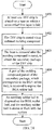
Fig. 3 is a specific flow chart of a secondary packaging method of a TSV chip according to a first embodiment of this disclosure; -
Fig. 4 is a sectional schematic diagram that the TSV chip is placed on a base according to the first embodiment of this disclosure; -
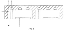
Fig. 5 is a sectional schematic diagram of a secondary package of a TSV chip, in which the base is removed, according to the first embodiment of this disclosure; -
Fig. 6 is a specific flow chart of a secondary packaging method of a TSV chip according to a second embodiment of this disclosure; -
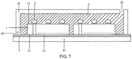
Fig. 7 is a structural schematic diagram of a first specific implementation mode for cladding the TSV chip via a softened molding compound according to the second embodiment of this disclosure; -
Fig. 8 is a specific flow chart of a secondary packaging method of a TSV chip according to a third embodiment of this disclosure; -
Fig. 9 is a structural schematic diagram of a second specific implementation mode for cladding the TSV chip via a softened molding compound according to the third embodiment of this disclosure; -
Fig. 10 is a specific flow chat of a secondary packaging method of a TSV chip according to a fourth embodiment of this disclosure; -
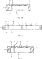
Fig. 11A is a structural schematic diagram of a first specific implementation mode for grinding a surface of a secondary package to expose a BGA solder ball according to the fourth embodiment of this disclosure; -
Fig. 11B is a sectional schematic diagram of a single unit of the secondary package of the TSV chip according to the fourth embodiment of this disclosure; -
Fig. 12 is a sectional schematic diagram of a secondary package of a TSV chip, in which an auxiliary solder ball is disposed on a BGA solder ball, according to a fifth embodiment of this disclosure; -
Fig. 13 is a sectional schematic diagram of a single unit of the secondary package of the TSV chip according to the fifth embodiment of this disclosure; -
Fig. 14 is a specific flow chat of a secondary packaging method of a TSV chip according to a sixth embodiment of this disclosure; -
Fig. 15 is a structural schematic diagram of an implementation mode for partially removing the molding compound to expose a BGA solder ball according to the sixth embodiment of this disclosure; -
Fig. 16 is a structural schematic diagram of partially removing the molding compound and adding an auxiliary solder ball according to the sixth embodiment of this disclosure; and -
Fig. 17 is a sectional schematic diagram of a single unit of the secondary package of the TSV chip according to the sixth embodiment of this disclosure. - In order to make objects, technical solutions and advantages of embodiments of this disclosure more apparent, each embodiment of this disclosure will be illustrated in detail in connection with the accompanying drawings. However, those skilled in the art can understand that in each embodiment of this disclosure, many technical details are proposed in order to make readers understand this disclosure better. But even if there are no those technical details and various changes and modifications based on each embodiment hereinafter, the technical solutions claimed for protection by this disclosure can also be implemented.
- A first embodiment of this disclosure relates to a secondary packaging method of a TSV chip, the specific process of which is as shown in
Fig. 3 . - S301: at least one TSV
chip 1 is placed on abase 41 on which a stressrelief film layer 3 is laid. - With reference to
Fig. 4 , the TSVchip 1 has aforward surface 11 and acounter surface 12 that are opposite to each other, and thecounter surface 12 is disposed with aBGA solder ball 2 thereon. In the embodiment, the TSV chip is a fingerprint identification chip, and theforward surface 11 further includes a fingerprintidentification sensing region 13. - In the secondary packaging process provided by the embodiment, the
base 41 is used for carrying the TSVchip 1. After the TSVchip 1 is placed on the stressrelief film layer 3, the stressrelief film layer 3 can take an effect of fixing theTSV chip 1 due to a certain viscosity. Theforward surface 11 of theTSV chip 1 includes the fingerprintidentification sensing region 13 and does not need to be packaged via a molding compound, and thus, theforward surface 11 is in contact with the stressrelief film layer 3. - A plurality of TSV
chips 1 can be simultaneously subjected to secondary packaging, a rule of placing the plurality ofTSV chips 1 on thebase 41 may be set according to actual demands. For example, placement spacing among the plurality of TSV chips or number of the TSV chips may be determined according to a size of the base 41 or demands on a size of a secondary package. - Preferably, the
forward surface 11 is provided with a protective layer (which is not shown in the figures), and the protective layer covers the fingerprintidentification sensing region 13 so as to protect the fingerprintidentification sensing region 13. The protective layer may have a thickness greater than or equal to 5 microns and smaller than or equal to 50 microns. For example, the thickness of the protective layer may be 5 microns, or 25 microns, or 50 microns; and a material of the protective layer may be organic colloid, and the protective layer may be coated on theforward surface 11. However, the embodiment does not limit the thickness, the material and the disposal manner of the protective layer. - S302: the
TSV chip 1 is coated via a softened molding compound. - In the step, for the
TSV chip 1, except that the forward surface 11 (including the fingerprint identification sensing region 13) is in contact with the stressrelief film layer 3, the other five surfaces are all plastic packaged by the softened molding compound. The softened molding compound generally contains organic and inorganic materials, such as resin, silicon oil, silicon dioxide particles and the like. - S303: the
base 41 is removed after the molding compound is cured, to obtain the secondary package of theTSV chip 1. - As shown in
Fig. 5 , in the case that a plurality ofTSV chips 1 are simultaneously arranged on a substrate, theTSV chips 1 are surrounded and supported by the cured molding compound. Since the cured molding compound has certain strength, the whole secondary package with a plurality ofTSV chips 1 can be formed. Since a bonding force between the stressrelief film layer 3 and the molding compound is not very large, the secondary package can be separated from the base 41 on which the stressrelief film layer 3 is laid, after the molding compound is cured, so as to obtain the secondary package of the TSV chip in a non-substrate form. - S304: the surface of the secondary package is processed to expose the
BGA solder ball 2. - At this time, the
BGA solder ball 2 is totally buried in the cured molding compound, and thus, theBGA solder ball 2 needs to be exposed out. The surface of the secondary package may be processed by a specific processing process, and the processed surface of the secondary package corresponds to thecounter surface 12 of theTSV chip 1; namely, theBGA solder ball 2 disposed on thecounter surface 12 of theTSV chip 1 is exposed, so that theTSV chip 1 is electrically interconnected with the outside only by theBGA solder ball 2. - It should be noted that, generally, in the case that the surface of the secondary package is processed, a part of the molding compound and a part of the BGA solder ball may be simultaneously removed; however, in some other cases, only the molding compound may be removed.
- In the case that the secondary package of a plurality of TSV chips is obtained, the conjoined secondary package of the plurality of TSV chips may be cut to obtain a single secondary package of a TSV chip, after the surface of the secondary package is processed to expose the BGA solder ball.
- Compared to the existing technology, in the secondary packaging method of the TSV chip provided by the embodiment, the secondary package in the non-substrate form can be obtained by employing the stress relief film layer and separating the secondary package of the TSV chip from the base on which the stress relief film layer is laid, after the molding compound is cured, so that based upon guaranteeing the TSV chip to have relatively high mechanical structural strength, the thickness of the secondary package of the TSV chip is reduced compared to that of a substrate packaging form, and the thinning and miniaturization design of an electronic product is facilitated.
- A second embodiment of this disclosure relates to a secondary packaging method of a TSV chip. The second embodiment is a refinement on the first embodiment, and the main refinement is that: with reference to
Fig. 6 andFig. 7 , the embodiment provides a first specific implementation mode for cladding theTSV chip 1 via softenedmolding compound 5, i.e., a method of injecting the molding compound by using an injection mold. - The specific flow of the secondary packaging method of the TSV chip, which is provided by the embodiment, is as shown in
Fig. 6 . - The step S601 is substantially the same as the step S301, and the step S603 to the step S604 are substantially the same as the step S303 to the step S304, which are not repeated herein; and the difference is that: the embodiment refines the step S302, and the specific description is as follows:
- In sub-step S6021, the
injection mold 42 with a cavity is pressed on thebase 41, and theTSV chip 1 is positioned in the cavity. - The stress
relief film layer 3 is laid on the base 41 in advance, and theinjection mold 42 is closed after theTSV chip 1 is placed well; then, a pressing force is applied to theinjection mold 42 from the outside, so that theinjection mold 42 and the base 41 are pressed together. - In sub-step S6022, the softened
molding compound 5 is injected into the cavity to clad theTSV chip 1 with themolding compound 5. - Actually, the
injection mold 42 is further provided with aninjection gate 44 and an exhaust port 43. In this case, theinjection gate 44 is used for injecting the softenedmolding compound 5 into the cavity, and the exhaust port 43 is used for discharging air in the cavity in the process of injecting themolding compound 5, so that themolding compound 5 can be full filled in the cavity to completely clad theTSV chip 1. - Compared to the first embodiment, the secondary packaging method of the TSV chip provided in the embodiment, provides a specific implementation mode for injecting the softened molding compound by using the injection mold to clad the TSV chip, and the injection mold is commonly used in the technical field and is simple and convenient in operation process.
- A third embodiment of this disclosure relates to a secondary packaging method of a TSV chip. The third embodiment is a refinement on the first embodiment, and the main refinement is that: with reference to
Fig. 8 andFig. 9 , the embodiment provides a second specific implementation mode for cladding the TSV chip via softened molding compound, i.e., a method of directly coating and pressing. - The specific flow of the secondary packaging method of the TSV chip provided in the embodiment is as shown in
Fig. 8 . - The step S801 is substantially the same as the step S301, and the step S803 to the step S804 are substantially the same as the step S303 to the step S304, which are not repeated herein; and the difference is that: the embodiment refines the step S302, and the specific description is as follows:
- In step S8021, the softened
molding compound 5 is coated on theTSV chip 1. - In the embodiment, after the
TSV chip 1 is placed on thebase 41 on which the stressrelief film layer 3 is laid, the softenedmolding compound 5 is directly coated on theTSV chip 1. - In step S8022, a
press mold 45 is used to press the softenedmolding compound 5 and theTSV chip 1 to clad the TSV chip with themolding compound 5. - In the embodiment, the
press mold 45 presses according to a direction shown by an arrow inFig. 9 and the redundant molding compound may overflow during the press process. After press, themolding compound 5 completely clads the five surfaces of theTSV chip 1 except for theforward surface 1 and full fills gaps among a plurality of TSV chips, and a flat glue surface can be obtained after the molding compound is cured. - It should be noted that the
press mold 45 in the embodiment may have no injection gate and exhaust port, and the technical solution in the embodiment can be implemented by directly utilizing a press effect of thepress mold 45. - It can be seen from the above-mentioned analysis that: the embodiment and the second embodiment of this disclosure respectively provide a specific implementation mode of cladding the TSV chip via softened molding compound; and the difference is that: in the second embodiment, according to the secondary packaging method of the TSV chip, the softened molding compound is injected into the injection mold to clad the TSV chip; while in this embodiment, the softened molding compound is directly coated on the surface of the TSV chip and pressed by utilizing the press mold. In actual applications, any method can be selected, and the embodiment does not make any limit thereto.
- Compared to the first embodiment, the secondary packaging method of the TSV chip provided by the embodiment provides a cladding mode of directly coating the softened molding compound on the TSV chip and pressing by utilizing the press mold; the press mold is commonly used in the technical field and is simple and convenient in operation process.
- A fourth embodiment of this disclosure relates to a secondary packaging method of a TSV chip. With reference to
Fig. 10, Fig. 11A andFig. 11B , the embodiment provides a first specific implementation mode for processing a surface of a secondary package to expose a BGA solder ball. - The specific flow of the secondary packaging method of the TSV chip provided in the embodiment is as shown in
Fig. 10 . - The step S1001 to the step S1003 are substantially the same as the step S301 to the step S303, and are not repeated herein; and the difference is that: the embodiment refines the step S304, and the specific description is as follows:
- In the step S1004, grinding is performed on the surface of the secondary package to expose the BGA solder ball.
- Since the
BGA solder ball 2 is still buried inside the curedmolding compound 5, according to the embodiment, the cured molding compound is ground to expose theBGA solder ball 2. - As shown in
Fig. 11A , in practice, a part of themolding compound 5 and a part of theBGA solder ball 2 may be ground. In the grinding process, a mechanical head of a grinding device directly applies a pressure on a surface (i.e., a surface corresponding to thecounter surface 12 of the TSV chip) of the secondary package, and the mechanical head rotates at a high speed after being powered up, so that a part of the surface of the secondary package may be ground and theBGA solder ball 2 is exposed, and a specific ground height actually depends on a height of the curedmolding compound 5. The exposed area of theBGA solder ball 2 may be maximized, to improve reliability of electrical connection of theBGA solder ball 2 and the outside to the greatest extent. In the embodiment, by taking a circular BGA solder ball (i.e., the exposed surface of the BGA solder ball is of a circle shape) as an example, it is preferable to grind a half of theBGA solder ball 2, and in this way, theBGA solder ball 2 has a maximum exposed area. That is, in this case, a distance between the exposed area of theBGA solder ball 2 and thecounter surface 12 of the TSV chip is equal to a radius of the circle.Fig. 11B shows a signal unit of the secondary package, which is obtained by cutting the secondary package of the plurality of TSV chips after grinding. - It is worth mentioning that the technical solution in the embodiment may be implemented on the basis of the second or third embodiment of this disclosure.
- Compared to the first embodiment, the secondary packaging method of the TSV chip provided in the embodiment provides a first specific implementation mode for processing the surface of the secondary package to expose the BGA solder ball, and the grinding process is commonly used in the technical field and is simple and convenient to operate and low in cost.
- A fifth embodiment of this disclosure relates to a secondary packaging method of a TSV chip, the embodiment is an improvement on the fourth embodiment, and the main improvement is that: with reference to
Fig. 12 and Fig. 13 , after processing the surface of the secondary package to expose theBGA solder ball 2, the secondary packaging method further includes a step of disposing anauxiliary solder ball 6 on the BGA solder ball so as to further improve reliability of electrical connection between theBGA solder ball 2 and the outside. - In practice, in the case that the part of the
BGA solder ball 2 is excessively ground or insufficiently ground in the grinding process, resulting in an insufficient area of the exposed surface of theBGA solder ball 2, or in the case that a maximized area of the exposed surface of theBGA solder ball 2 still cannot meet the actual design demand of the electronic product (i.e., the exposed area of theBGA solder ball 2 is still not big enough), theBGA solder ball 2 may be disposed with theauxiliary solder ball 6 thereon by adopting a silk-screen printing process, and the secondary package of the TSV chip is obtained after a solder reflowing process. Theauxiliary solder ball 6 is above the surface of the secondary package, which is equivalent to increasing the exposed area of theBGA solder ball 2, so that the reliability of electrical connection between theBGA solder ball 2 and the outside is further improved.Fig. 13 shows a single unit of the secondary package of the TSV chip, which is obtained by cutting after disposing theauxiliary solder ball 6. - It is worth mentioning that the technical solution in the embodiment may be implemented on the basis of the second or third embodiment of this disclosure.
- Compared to the fourth embodiment, the secondary packaging method of the TSV chip provided by the embodiment further improves the reliability of electrical connection between the BGA solder ball and the outside by adding the auxiliary solder ball.
- A sixth embodiment of this disclosure relates to a secondary packaging method of a TSV chip. The fifth embodiment is a refinement on the first embodiment, and the main refinement is that: with reference to
Fig. 14 andFig. 15 , the embodiment provides a second specific implementation mode for processing the surface of the secondary package to expose the BGA solder ball. - The specific flow of the second packaging method of the TSV chip provided by the embodiment is as shown in
Fig. 14 . - The step S1401 to the step S1403 are substantially the same as the step S301 to the step S303, and are not repeated herein; and the difference is that: the embodiment refines the step S304, and adds a step S1405, and the specific description is as follows:
- In the step S1404, a part of the molding compound partial of the secondary package, which corresponds to the
BGA solder ball 2, is removed to expose theBGA solder ball 2. - As shown in
Fig. 15 , in the embodiment, the part of the molding compound may be removed by adopting one or any combination of a laser method, an ion bombardment method and a chemical corrosion method. Due to process characteristics, in the embodiment, only the part of the molding compound, which corresponds to theBGA solder ball 2, is removed, so that acavity region 21 is formed above theBGA solder ball 2. These processes may be used for removing unwanted material in the secondary package, but not theBGA solder ball 2. - In the step S1405, an
auxiliary solder ball 6 is disposed on the BGA solder ball, and theauxiliary solder ball 6 is above or flush with the surface. - As shown in
Fig. 16 , since the exposed surface of theBGA solder ball 2 is lower than the surface of the secondary package, in the embodiment, theauxiliary solder ball 6 needs to be disposed and fills into thecavity region 21 corresponding to eachBGA solder ball 2. In practice, it may adopt a silk-screen printing process to print solder into a cavity region, or a ball drop process to directly fill thecavity region 21 with a solder ball and a reflowing process to completely fill thecavity region 21. In the case of disposing theauxiliary solder ball 6, theauxiliary solder ball 6 shall be above or flush with the surface so as to facilitate the electrical connection between the secondary package and the outside.Fig. 17 shows a single unit of the secondary package of the TSV chip, which is obtained by cutting after disposing theauxiliary solder ball 6. - It can be seen from the above-mentioned analysis that: the embodiment and the fourth embodiment of this disclosure respectively provide a specific implementation mode for processing the surface of the secondary package to expose the BGA solder ball. The difference is that: firstly, in the fourth embodiment of this disclosure, for processing the surface of the secondary package, the grinding process is adopted, by which a part of the
molding compound 5 and a part of theBGA solder ball 2 may be simultaneously ground, or only themolding compound 5 may be ground; however, in this embodiment, for processing the surface of the secondary package, only the part of themolding compound 5, which corresponds to theBGA solder ball 2, is removed, while leaving theBGA solder ball 2. Secondly, in the fourth embodiment of this disclosure, theauxiliary solder ball 6 may be used as an alternative; however, in this embodiment, theauxiliary solder ball 6 is necessary. - It is worth mentioning that the technical solution in the embodiment may also be implemented on the basis of the second or third embodiment of this disclosure.
- Compared to the first embodiment, the second packaging method of the TSV chip provided by the embodiment provides a second specific implementation mode for processing the surface of the second package to expose the BGA solder ball, and the process of partially removing the molding compound and the process of disposing the auxiliary solder ball are commonly used in the technical field and very simple to implement.
- The step division of various processes and methods above is just for clear description, and in practical operations, the steps can be merged into one step or some steps can be split to be decomposed into a plurality of steps.
- A seventh embodiment of this disclosure relates to a secondary package of a TSV chip. With reference to
Fig. 11 , the secondary package of the TSV chip includes: aTSV chip 1 and amolding compound 2; theTSV chip 1 has aforward surface 11, ancounter surface 12 and a plurality of side surfaces; thecounter surface 12 of theTSV chip 1 is disposed with asolder ball 2 thereon; and themolding compound 5 clads thecounter surface 12 and the plurality of side surfaces of theTSV chip 1, and thesolder ball 2 is exposed out of the surface of themolding compound 5. - In the embodiment, the
TSV chip 1 is a fingerprint identification chip, and theforward surface 11 of theTSV chip 1 further includes a fingerprintidentification sensing region 13. The solder ball includes aBGA solder ball 2, theBGA solder ball 2 is exposed out of the surface of themolding compound 5, and the exposed surface of theBGA solder ball 2 is flush with the surface of themolding compound 5, so that theBGA solder ball 2 may be electrically interconnected with the outside. - In practice, in the case of processing the surface of the secondary package of the TSV chip, a part of the molding compound and a part of the BGA solder ball may be removed by adopting a grinding process, so as to expose the
BGA solder ball 2 of the surface of themolding compound 5. - Preferably, the exposed surface of the
BGA solder ball 2 is of a circle shape, and a distance between the exposed surface of theBGA solder ball 2 and thecounter surface 12 of theTSV chip 1 is equal to a radius of the circle, and in this case, theBGA solder ball 2 has a maximum area of the exposed surface, and the reliability of electrical connection between theBGA solder ball 2 and the outside is improved to the greatest extent. - Compared to the existing technology, according to the secondary package of the TSV chip provided by the embodiment, the secondary package in the non-substrate form can be obtained by employing the stress relief film layer and separating the secondary package of the TSV chip from the base on which the stress relief film layer is laid, after the molding compound is cured, so that based upon guaranteeing the TSV chip to have relatively high mechanical structural strength, the thickness of the secondary package of the TSV chip is reduced compared to that of a substrate packaging form, and the thinning and miniaturization design of an electronic product is facilitated.
- An eighth embodiment of this disclosure relates to a secondary package of a TSV chip, the embodiment is substantially the same as the sixth embodiment, and the main difference is that: in the seventh embodiment of this disclosure, the solder ball includes the
BGA solder ball 2, and theBGA solder ball 2 is exposed out of the surface of themolding compound 5, and the exposed surface of theBGA solder ball 2 is flush with the surface of themolding compound 5; however, in this embodiment, with reference toFig. 13 or17 , the solder ball includes aBGA solder ball 2 and anauxiliary solder ball 6, theauxiliary solder ball 6 is exposed out of the surface of themolding compound 5, and the exposed surface of theauxiliary solder ball 6 is above or flush with the surface of themolding compound 5. - In the embodiment, the
BGA solder ball 2 is connected to thecounter surface 12 of the TSV chip, and after the secondary package is obtained, the surface of the secondary package of the TSV chip is processed to expose theBGA solder ball 2. In practice, the molding compound corresponding to theBGA solder ball 2 may be removed by adopting one or any combination of a laser method, an ion bombardment method and a chemical corrosion method. Due to process characteristics, the BGA solder ball is not removed by adopting these processes, and thus, in this case, the exposed surface of the BGA solder ball is lower than the surface of the secondary package, and theauxiliary solder ball 6 needs to be disposed on theBGA solder ball 2, to connect theBGA solder ball 2 with theauxiliary solder ball 6, and to expose theauxiliary solder ball 6 out of the surface of themolding compound 5, i.e., the exposed surface of theauxiliary solder ball 6 is above or flush with the surface of themolding compound 5. - Preferably, when the exposed surface of the
auxiliary solder ball 6 is above the surface of themolding compound 5, the exposed surface of theauxiliary solder ball 6 is above the surface of themolding compound 5 by a distance of 50 um to 300 um, so that the auxiliary solder ball has the sufficient exposed area to ensure reliability of electrical connection with the outside, and meanwhile, a whole thickness of the secondary package of the TSV chip is as small as possible. - Compared to the seventh embodiment, the secondary package of the TSV chip provided by the embodiment provides a second specific implementation mode for the secondary package of the TSV chip, that is, the BGA solder ball is disposed with the auxiliary solder ball thereon, to increase the contact area between the BGA solder ball and the outside, so that the reliability of electrical connection is improved.
- Those skilled in the art can understand that each of the above-mentioned embodiments is the specific embodiment for implementing this disclosure, but in practical applications, various changes can be made to the embodiments in form and in detail, without departure from the spirit and scope of this disclosure.
Claims (17)
- A secondary packaging method of a through silicon via (TSV) chip, characterized in that, the TSV chip has a forward surface and a counter surface that are opposite to each other, the counter surface is disposed with a ball grid array (BGA) solder ball thereon, the secondary packaging method of the TSV chip comprises:placing at least one TSV chip on a base on which a stress relief film layer is laid; wherein the forward surface of the TSV chip is in contact with the stress relief film layer;cladding the TSV chip via a softened molding compound;removing the base after the molding compound is cured, to obtain a secondary package of the TSV chip; andprocessing a surface of the secondary package to expose the BGA solder ball; wherein the processed surface of the secondary package corresponds to the counter surface of the TSV chip.
- The secondary packaging method of the TSV chip according to claim 1, characterized in that, the step of cladding the TSV chip via the softened molding compound specifically comprises:pressing an injection mold with a cavity on the base, to position the TSV chip in the cavity; andinjecting the softened molding compound into the cavity, to clad the TSV chip with the molding compound.
- The secondary packaging method of the TSV chip according to claim 1, characterized in that, the step of cladding the TSV chip via the softened molding compound specifically comprises:coating the TSV chip with the softened molding compound; andpressing the softened molding compound and the TSV chip by utilizing a press mold, to clad the TSV chip with the molding compound.
- The secondary packaging method of the TSV chip according to any one of claims 1 to 3, characterized in that, the step of processing the surface of the secondary package to expose the BGA solder ball specifically comprises:
grinding the surface of the secondary package to expose the BGA solder ball. - The secondary packaging method of the TSV chip according to claim 4, characterized in that, the BGA solder ball has a circle shaped exposed surface, and a distance between the exposed surface of the BGA solder ball and the counter surface of the TSV chip is equal to a radius of the circle.
- The secondary packaging method of the TSV chip according to claim 4 or 5, characterized by further comprising: disposing an auxiliary solder ball on the BGA solder ball after the step of processing the surface of the secondary package to expose the BGA solder ball; wherein the auxiliary solder ball is above the surface.
- The secondary packaging method of the TSV chip according to any one of claims 1 to 3, characterized in that, the step of processing the surface of the secondary package to expose the BGA solder ball specifically comprises:partially removing a part of the molding compound of the secondary package, which corresponds to the BGA solder ball, to expose the BGA solder ball;the secondary packaging method further comprises: disposing an auxiliary solder ball on the BGA solder ball after the step of processing the surface of the secondary package to expose the BGA solder ball, and the auxiliary solder ball is above or flush with the surface.
- The secondary packaging method of the TSV chip according to claim 7, characterized in that, a method for the partial removal comprises one or any of a laser method, an ion bombardment method and a chemical corrosion method.
- The secondary packaging method of the TSV chip according to any one of claims 1 to 8, characterized in that, a plurality of TSV chips are provided, and the secondary packaging method further comprises: cutting the secondary package to obtain a single secondary package of a TSV chip, after the step of processing the surface of the secondary package to expose the BGA solder ball.
- A secondary package of a TSV chip, characterized by comprising: a TSV chip and a molding compound;
the TSV chip has a forward surface, a counter surface and a plurality of side surfaces; the counter surface of the TSV chip is disposed with a solder ball thereon; and
the molding compound clads the counter surface and the plurality of side surfaces of the TSV chip, and the solder ball is exposed out of a surface of the molding compound. - The secondary package of the TSV chip according to claim 10, characterized in that, the solder ball comprises a BGA solder ball; and
the BGA solder ball is exposed out of the surface of the molding compound, and the exposed surface of the BGA solder ball is flush with the surface of the molding compound. - The secondary package of the TSV chip according to claim 11, characterized in that, the exposed surface of the BGA solder ball is of a circle shape, and a distance between the exposed surface of the BGA solder ball and the counter surface of the TSV chip is equal to a radius of the circle.
- The secondary package of the TSV chip according to claim 10, characterized in that, the solder ball comprises a BGA solder ball and an auxiliary solder ball, the BGA solder ball is connected to the counter surface of the TSV chip, and the auxiliary solder ball is connected to the BGA solder ball; and
the auxiliary solder ball is exposed out of the surface of the molding compound, and the exposed surface of the auxiliary solder ball is above or flush with the surface of the molding compound. - The secondary package of the TSV chip according to claim 13, characterized in that, when the exposed surface of the auxiliary solder ball is above the surface of the molding compound, the exposed surface of the auxiliary solder ball is above the surface of the molding compound by a distance of 50 um to 300 um.
- The secondary package of the TSV chip according to any one of claims 10 to 14, characterized in that, the TSV chip is a fingerprint identification chip, and the forward surface of the TSV chip comprises a fingerprint identification sensing region.
- The secondary package of the TSV chip according to claim 15, characterized in that, the forwarding surface of the TSV chip is provided with a protective layer, and the protective layer covers the fingerprint identification sensing region.
- The secondary package of the TSV chip according to claim 16, characterized in that, the protective layer has a thickness greater than or equal to 5 microns, and smaller than or equal to 50 microns.
Applications Claiming Priority (2)
| Application Number | Priority Date | Filing Date | Title |
|---|---|---|---|
| CNPCT/CN2017/073354 | 2017-02-13 | ||
| PCT/CN2017/094695 WO2018145413A1 (en) | 2017-02-13 | 2017-07-27 | Secondary packaging method for through-silicon via chip and secondary package thereof |
Publications (2)
| Publication Number | Publication Date |
|---|---|
| EP3422397A1 true EP3422397A1 (en) | 2019-01-02 |
| EP3422397A4 EP3422397A4 (en) | 2019-07-31 |
Family
ID=63107896
Family Applications (1)
| Application Number | Title | Priority Date | Filing Date |
|---|---|---|---|
| EP17896308.8A Ceased EP3422397A4 (en) | 2017-02-13 | 2017-07-27 | METHOD FOR SECONDARY ENCLOSURE OF INTERCONNECTION HOLE CHIP THROUGH SILICON AND ITS SECONDARY HOUSING |
Country Status (4)
| Country | Link |
|---|---|
| US (1) | US11183414B2 (en) |
| EP (1) | EP3422397A4 (en) |
| CN (1) | CN108780772B (en) |
| WO (1) | WO2018145413A1 (en) |
Families Citing this family (5)
| Publication number | Priority date | Publication date | Assignee | Title |
|---|---|---|---|---|
| CN112331568B (en) * | 2020-11-04 | 2022-12-23 | 青岛歌尔微电子研究院有限公司 | Chip glue overflow prevention packaging method |
| TWM612841U (en) * | 2021-02-19 | 2021-06-01 | 安帝司股份有限公司 | Fingerprint identification smart card |
| CN114055711B (en) * | 2021-11-18 | 2024-05-28 | 江苏芯德半导体科技有限公司 | Chip plastic packaging mold and secondary plastic packaging process method thereof |
| CN114284158A (en) * | 2021-12-06 | 2022-04-05 | 立讯电子科技(昆山)有限公司 | Double-sided packaging structure and manufacturing method thereof |
| CN119864324B (en) * | 2025-03-25 | 2025-07-01 | 合肥沛顿存储科技有限公司 | Process method for taking out and recycling chip in flip chip packaging structure |
Family Cites Families (36)
| Publication number | Priority date | Publication date | Assignee | Title |
|---|---|---|---|---|
| KR100246333B1 (en) | 1997-03-14 | 2000-03-15 | 김영환 | Ball grid array package and method for manufacturing thereof |
| JP4702586B2 (en) * | 2001-09-10 | 2011-06-15 | 日本電気株式会社 | Fingerprint sensor, fingerprint sensor mounting structure, and fingerprint detector having the fingerprint sensor |
| TW506097B (en) * | 2001-10-17 | 2002-10-11 | Apack Technologies Inc | Wafer level chip scale package structure and its manufacturing method |
| US7626269B2 (en) * | 2006-07-06 | 2009-12-01 | Micron Technology, Inc. | Semiconductor constructions and assemblies, and electronic systems |
| CN100565828C (en) | 2007-04-16 | 2009-12-02 | 日月光半导体制造股份有限公司 | sealing method of sensor chip |
| CN101465299B (en) * | 2007-12-20 | 2011-06-15 | 南茂科技股份有限公司 | Die Reconfigurable Packaging Structure Using Grinding Manufacturing Method |
| US8236609B2 (en) * | 2008-08-01 | 2012-08-07 | Freescale Semiconductor, Inc. | Packaging an integrated circuit die with backside metallization |
| US9196571B2 (en) * | 2010-01-13 | 2015-11-24 | Xintec Inc. | Chip device packages and fabrication methods thereof |
| US8362612B1 (en) | 2010-03-19 | 2013-01-29 | Amkor Technology, Inc. | Semiconductor device and manufacturing method thereof |
| US8717775B1 (en) * | 2010-08-02 | 2014-05-06 | Amkor Technology, Inc. | Fingerprint sensor package and method |
| KR101789765B1 (en) * | 2010-12-16 | 2017-11-21 | 삼성전자주식회사 | Semiconductor device and method of forming the same |
| US8642385B2 (en) * | 2011-08-09 | 2014-02-04 | Alpha & Omega Semiconductor, Inc. | Wafer level package structure and the fabrication method thereof |
| US8922013B2 (en) | 2011-11-08 | 2014-12-30 | Stmicroelectronics Pte Ltd. | Through via package |
| CN103208430B (en) | 2012-01-17 | 2015-09-30 | 万国半导体股份有限公司 | Utilize hot pressing soldered ball in wafer scale plastic package process, realize the method for ultra-thin chip |
| JP5728423B2 (en) * | 2012-03-08 | 2015-06-03 | 株式会社東芝 | Semiconductor device manufacturing method, semiconductor integrated device, and manufacturing method thereof |
| KR101902996B1 (en) * | 2012-07-09 | 2018-10-01 | 삼성전자주식회사 | Semiconductor package and method of forming the same |
| JP6364626B2 (en) * | 2013-07-29 | 2018-08-01 | パナソニックIpマネジメント株式会社 | Diffraction optical element, method of manufacturing diffractive optical element, and mold used for manufacturing method of diffractive optical element |
| KR20150121759A (en) | 2014-04-21 | 2015-10-30 | 에스티에스반도체통신 주식회사 | Stacked package and method for manufacturing the same |
| US9437566B2 (en) | 2014-05-12 | 2016-09-06 | Invensas Corporation | Conductive connections, structures with such connections, and methods of manufacture |
| CN104102902B (en) * | 2014-07-04 | 2017-07-04 | 京东方科技集团股份有限公司 | A kind of semiconductor fingerprint identification sensor and its manufacture method |
| CN204011397U (en) | 2014-08-26 | 2014-12-10 | 南昌欧菲生物识别技术有限公司 | Capacitive fingerprint sensor encapsulating structure |
| CN104201115A (en) * | 2014-09-12 | 2014-12-10 | 苏州晶方半导体科技股份有限公司 | Wafer-level fingerprint recognition chip packaging structure and method |
| TWI582918B (en) * | 2014-11-12 | 2017-05-11 | 精材科技股份有限公司 | Chip package and method of manufacturing same |
| CN104576424A (en) * | 2014-12-10 | 2015-04-29 | 华进半导体封装先导技术研发中心有限公司 | Method for realizing fan-out wafer encapsulation by preparing bumps on chip in advance |
| CN104485320A (en) * | 2014-12-30 | 2015-04-01 | 华天科技(西安)有限公司 | Embedded sensing chip encapsulation structure with vertical through hole and manufacturing method thereof |
| CN104538373B (en) | 2014-12-30 | 2017-05-03 | 华天科技(昆山)电子有限公司 | Three-dimensional integrated sensor chip packaging structure and packaging method |
| CN104495741B (en) | 2014-12-30 | 2018-05-01 | 华天科技(昆山)电子有限公司 | Surface sensing chip encapsulating structure and production method |
| CN105810599A (en) * | 2014-12-30 | 2016-07-27 | 深南电路有限公司 | Substrate embedded with fingerprint identification chip and processing method thereof |
| CN107039369A (en) | 2015-01-23 | 2017-08-11 | 三星半导体(中国)研究开发有限公司 | Encapsulation includes the encapsulation stacking structure and its manufacture method of the encapsulation |
| TWI614881B (en) * | 2015-01-28 | 2018-02-11 | 精材科技股份有限公司 | Photosensitive module and method of manufacturing same |
| US9966358B2 (en) * | 2015-06-17 | 2018-05-08 | Xintec Inc. | Chip package |
| CN105390429A (en) * | 2015-11-05 | 2016-03-09 | 南通富士通微电子股份有限公司 | Packaging method |
| US9898645B2 (en) * | 2015-11-17 | 2018-02-20 | Taiwan Semiconductor Manufacturing Company, Ltd. | Fingerprint sensor device and method |
| TWI584418B (en) * | 2016-05-16 | 2017-05-21 | 神盾股份有限公司 | Fingerprint sensor and packaging method thereof |
| CN106098717B (en) | 2016-08-05 | 2023-07-18 | 华天科技(昆山)电子有限公司 | High reliability chip packaging method and structure |
| CN207038516U (en) | 2017-02-13 | 2018-02-23 | 深圳市汇顶科技股份有限公司 | The secondary package of silicon hole chip |
-
2017
- 2017-07-27 EP EP17896308.8A patent/EP3422397A4/en not_active Ceased
- 2017-07-27 CN CN201780010390.2A patent/CN108780772B/en active Active
- 2017-07-27 WO PCT/CN2017/094695 patent/WO2018145413A1/en not_active Ceased
-
2018
- 2018-09-24 US US16/139,994 patent/US11183414B2/en active Active
Also Published As
| Publication number | Publication date |
|---|---|
| US20190027390A1 (en) | 2019-01-24 |
| CN108780772A (en) | 2018-11-09 |
| WO2018145413A1 (en) | 2018-08-16 |
| CN108780772B (en) | 2023-07-14 |
| US11183414B2 (en) | 2021-11-23 |
| EP3422397A4 (en) | 2019-07-31 |
Similar Documents
| Publication | Publication Date | Title |
|---|---|---|
| US11183414B2 (en) | Secondary packaging method and secondary package of through silicon via chip | |
| US20240385398A1 (en) | Optical transceiver and manufacturing method thereof | |
| US8803332B2 (en) | Delamination resistance of stacked dies in die saw | |
| US9117828B2 (en) | Method of handling a thin wafer | |
| US9425177B2 (en) | Method of manufacturing semiconductor device including grinding semiconductor wafer | |
| US20200115220A1 (en) | Wafer-level fan-out package with enhanced performance | |
| CN107275294A (en) | Thin chip stack package structure and manufacturing method thereof | |
| JP2003115560A (en) | Semiconductor device, stacked semiconductor device, method of manufacturing semiconductor device, and method of manufacturing stacked semiconductor device | |
| CN106560918A (en) | Semiconductor packaging structure and forming method thereof | |
| CN107818922B (en) | Method of manufacturing semiconductor package | |
| CN102760713A (en) | Chip-packaging module for a chip and a method for forming a chip-packaging module | |
| CN111863641A (en) | A chip packaging method | |
| JP2008028325A (en) | Method of manufacturing semiconductor device | |
| US20080105942A1 (en) | Sensor-type semiconductor package and fabrication method thereof | |
| US20130215583A1 (en) | Embedded Electrical Component Surface Interconnect | |
| CN116264211A (en) | Semiconductor package and manufacturing method thereof | |
| CN108074827A (en) | Fingerprint identification module and manufacturing method thereof | |
| US11501553B2 (en) | Cost-efficient fingerprint sensor component and manufacturing method | |
| CN107910274A (en) | A kind of method for packing and encapsulating structure of fingerprint chip | |
| US20120326332A1 (en) | Semiconductor device with encapsulated electrical connection elements and fabrication process thereof | |
| CN114649219A (en) | Semiconductor device and method for manufacturing the same | |
| CN104103536A (en) | Package-on-package (POP) packaging method | |
| US20210335628A1 (en) | Flip-chip package with reduced underfill area | |
| CN207038516U (en) | The secondary package of silicon hole chip | |
| CN110797334A (en) | Semiconductor device and method for manufacturing the same |
Legal Events
| Date | Code | Title | Description |
|---|---|---|---|
| STAA | Information on the status of an ep patent application or granted ep patent |
Free format text: STATUS: THE INTERNATIONAL PUBLICATION HAS BEEN MADE |
|
| PUAI | Public reference made under article 153(3) epc to a published international application that has entered the european phase |
Free format text: ORIGINAL CODE: 0009012 |
|
| STAA | Information on the status of an ep patent application or granted ep patent |
Free format text: STATUS: REQUEST FOR EXAMINATION WAS MADE |
|
| 17P | Request for examination filed |
Effective date: 20180925 |
|
| AK | Designated contracting states |
Kind code of ref document: A1 Designated state(s): AL AT BE BG CH CY CZ DE DK EE ES FI FR GB GR HR HU IE IS IT LI LT LU LV MC MK MT NL NO PL PT RO RS SE SI SK SM TR |
|
| AX | Request for extension of the european patent |
Extension state: BA ME |
|
| A4 | Supplementary search report drawn up and despatched |
Effective date: 20190627 |
|
| RIC1 | Information provided on ipc code assigned before grant |
Ipc: H01L 21/56 20060101ALI20190621BHEP Ipc: H01L 23/31 20060101AFI20190621BHEP |
|
| DAV | Request for validation of the european patent (deleted) | ||
| DAX | Request for extension of the european patent (deleted) | ||
| STAA | Information on the status of an ep patent application or granted ep patent |
Free format text: STATUS: EXAMINATION IS IN PROGRESS |
|
| 17Q | First examination report despatched |
Effective date: 20200702 |
|
| REG | Reference to a national code |
Ref country code: DE Ref legal event code: R003 |
|
| STAA | Information on the status of an ep patent application or granted ep patent |
Free format text: STATUS: THE APPLICATION HAS BEEN REFUSED |
|
| 18R | Application refused |
Effective date: 20211103 |